
 Open Access Article
 This Open Access Article is licensed under a
 Creative Commons Attribution 3.0 Unported Licence
Cytocompatible, disintegrable, low-voltage operation n-type organic thin film transistors†
Mohsin
Ali
 a,
Bahar
Ronnasi
a,
May
Ourabi
a,
Joon Hyung
Park
b,
Jean-Philippe
St-Pierre
a,
Chang-Hyun
Kim
c and
Benoît H.
Lessard
*ac
a,
Bahar
Ronnasi
a,
May
Ourabi
a,
Joon Hyung
Park
b,
Jean-Philippe
St-Pierre
a,
Chang-Hyun
Kim
c and
Benoît H.
Lessard
*ac
aDepartment of Chemical and Biological Engineering, University of Ottawa, 161 Louis Pasteur, Ottawa, ON, Canada. E-mail: benoit.lessard@uottawa.ca
bSchool of Electronic Engineering, Gachon University, Seongnam 13120, Republic of Korea
cSchool of Electrical Engineering and Computer Science, University of Ottawa, 800 King Edward Ave., Ottawa, ON, Canada
First published on 23rd December 2024
Abstract
The constant demands for the better performance of consumer electronics have led to shorter usage lifespans, resulting in a significant increase in electronic waste (e-waste). Developing electronics that can be easily broken down and recycled is a promising strategy to tackle this growing e-waste challenge. Herein, we report a biocompatible and degradable organic thin film transistor (OTFT) utilizing a biocompatible semiconductor with a biodegradable dielectric and substrate. We present the first OTFT based on bispentafluorophenoxy silicon phthalocyanine (F10-SiPc) integrated with a polyvinyl alcohol (PVA) and poly(caprolactone) (PCL) bilayer as the dielectric, leading to a drop in threshold voltage (VT) from 12.7 V to −0.97 V, versus using SiO2 while maintaining similar mobility values. We demonstrate the importance of the annealing temperature on PLA substrate roughness and gate electrode surface chemistry for the fabrication of working OTFT devices. We then demonstrate that the bendable OTFTs could easily be dissolved in phosphate buffer saline (PBS) solution at room temperature in less than a month, which is a crucial aspect for ensuring eco-sustainability in electronic devices. Finally, incubation of the degradation products with fibroblastic cells did not affect cell viability, suggesting that they are non-cytotoxic. These cytocompatible disintegrable OTFTs with low operating voltages will find applications in bioresorbable electronics and constitute a step towards minimizing e-waste.
Introduction
In 2021, the United Nations released a report estimating that every person will produce roughly 7.6 kg of e-waste, leading to 57.4 million metric tonnes (MMT)1 of e-waste. This number is predicted to rise to 74 MMT by 2030 if left uncontrolled. The need to consider the environmental effects of essential electronic components like transistors and capacitors during production and disposal is growing due to the increasing demand for these devices worldwide. Sustainable and environmentally friendly electronics are becoming increasingly important, from reducing the risks linked to e-waste to paving the way for the generation of new wearable and implantable electronics.2–5 The growing number of transient electronic applications such as food package sensors or single-use biosensors is also causing concern for the e-waste problem and providing an opportunity for the development of non-toxic biodegradable electronics.6,7The use of thin, plastic substrates in the fabrication of electrical devices has the advantage of lowering the total mass of the systems and imparting flexible characteristics which can lead to new applications such as wearable electronics.8,9 Nevertheless, there are intrinsic disadvantages to using plastic substrates, including their disintegration into microplastics that can then find their way into our soil and groundwater, contributing to environmental contamination.10 Consequently, the use of plastic substrates in flexible electronics that are not biodegradable or recyclable is unsustainable.11 One of the challenges associated with using biodegradable substrates such as poly(lactic acid) (PLA) is that the glass transition temperature (Tg) of these materials is very low, which makes it challenging to integrate them into high-temperature manufacturing processes like the manufacturing of silicon semiconductors. For organic electronics, the semiconductor is carbon-based and can be deposited at lower temperatures, enabling integration onto plastic substrates while providing low energy requirements and potential economic incentives.12 Organic thin film transistors (OTFTs) are electrical switches and are basic components in more complex circuits finding applications in next generation biological and chemical sensors,13 health monitors,14 stretchable devices,15 and electronic skin.16 Research on OTFT development has focused primarily on improving device performance with little attention to assessing the biocompatibility and environmental impact of the resulting materials.17,18
Biodegradable OTFTs require biodegradable substrates, dielectrics, electrodes, semiconductors, and peripheral materials such as encapsulating materials. Biobased materials, such as PLA, polyhydroxyalkanoates (PHAs), starch blends, or cellulose-based polymers, are promising substrates if the processing temperatures can be kept <150 °C.19 However, biodegradable dielectrics with the desired physical and electrical properties are rare. Poly(vinyl alcohol) (PVA) is a bioresorbable dielectric that can be easily dissolved in environmentally friendly solvents such as water and breaks down naturally when exposed to suitable microorganisms.20 PVA has been previously used as a dielectric material in sensors21 and OTFTs, either as a homopolymer or as a blend of other materials.22,23 However, PVA also presents challenges; its printing is difficult often requiring careful optimization such as the addition of a viscosity enhancer24 and the resulting hydrophilic film is susceptible to moisture resulting in reduced reliability and stability of fabricated devices.25,26 Our group recently developed PVA with an interfacial, thermally crosslinked diisocyanate-terminated polycaprolactone (TPCL) leading to high-k/low-k bilayer dielectrics. The bilayer combined the desired electrical properties and high dielectric constant of the PVA with the moisture resistance of PCL, which also provides better surface matching for the subsequent deposition of the semiconductor. To further improve the shelf life and the ease of large-scale processing we then synthesized benzodioxinone-terminated PCL layer, which can be coupled to the PVA dielectric surface via UV radiation.27 High-k/low-k bilayer dielectrics have shown several advantages, such as reduced charge trapping, improved device stability, facilitation of orthogonal processing, and prevention of direct interaction between the hydroxyl groups of PVA and the semiconductor.28–30 The PCL layer acts as a protective coating for the PVA layer, creating a less polar environment at the interface between the dielectric and semiconductor.31,32
Phthalocyanines (Pcs) are promising semiconductors used in OTFTs that are produced on the ton scale annually and are commonly used as blue and green pigments in a variety of applications, including textiles, plastics, automotive paints, and others.33–35 Silicon phthalocyanines (R2-SiPcs) are a class of tetravalent Pc with axial groups that can be used as handles to impart functionalities onto the molecule such as solubility or solid state engineering amenability. Their strong near-infrared (NIR) emission has also stimulated their prospective use in both in vitro and in vivo bioimaging.36–40 Our group has demonstrated relatively better n-type performance of various R2-SiPc derivatives in OTFTs.41–45 In most cases R2-SiPc-based OTFTs suffer from high threshold voltage (VT) making them unsuitable for use in consumer electronics (<3 V) or in combination with printed batteries (<1.5 V).46,47 The interface between dielectrics and semiconductors in OTFT devices plays a pivotal role in enhancing charge transport by mitigating charge traps and reducing VT.48–50 Hybrid gate dielectric combinations of inorganic/organic bilayers are commonly employed to achieve high-performance organic transistors.51 However these materials are non-degradable suggesting the need for biodegradable materials with a high dielectric constant (k). Recently, our group published the first R2-SiPc paired with a polymer dielectric based on methyl methacrylate and dimethyl aminoethyl methacrylate copolymers (P(MMA-co-DMAEMA)), attaining near-zero VT.52 While not biodegradable, this study demonstrates the potential for using polymer dielectrics in combination with R2-SiPc semiconductors in OTFTs.
In this work, we present a disintegrable and biocompatible n-type OTFT with a low VT, based on the R2-SiPc OTFT utilizing a biodegradable bilayer PVA/UV-PCL as a gate dielectric with a biodegradable PLA substrate. Utilizing UV-PCL increased device stability and ease of processing while maintaining its encapsulation characteristics and moisture resistance for the PVA layer. We also demonstrate the aqueous disintegration of the resulting OTFTs into non-cytotoxic degradation products. These results demonstrate the broad applicability of low-voltage n-type and bioresorbable polymer dielectrics that employ scalable, economically viable R2-SiPc semiconductors.
Results and discussion
In selecting active materials, we focused on utilizing polymers that exhibit biocompatibility, biodegradability, and adequate electrical properties, and are soluble in various solvent systems enabling solution processing into thin films. Fig. 1 shows schematically the design of biocompatible and disintegrable OTFTs fabricated with bottom-gate top-contact (BGTC) architecture based on a PLA substrate, a bilayer PVA/PCL dielectric and an R2-SiPc semiconductor. The substrate, which makes up 99.89% of the overall mass of the device,53 was chosen to be made of PLA, a linear biodegradable thermoplastic polyester. The physical attributes of PLA provided constraints for further device processing as a result of (i) a low melting point (Tm) and low Tg, and (ii) low chemical resistance when exposed to organic solvents and incompatibility with orthogonal processing. These characteristics indicate the need to use mild downstream processing conditions. Here, we employ water-soluble PVA as a solution-processable dielectric. PLA, PVA, and PCL are economical, easily accessible, and have a well-established history in various biomedical devices used in clinical settings.53 The development of ecologically benign semiconductor materials is another critical step to overcome when fabricating fully decomposable OTFT devices.54 R2-SiPcs exhibit non-hazardous and biocompatible properties, making them promising candidates for degradable OTFTs. Gold electrodes are used in the OTFTs due to their remarkable conductivity and biocompatible characteristics both in vitro and in vivo and because gold has been employed in a range of medical applications.55–57 Gold, as an inert biomaterial, has demonstrated decreased biofouling in living organisms for various biomedical implants, such as cardiovascular58 and biomedical microelectromechanical (BioMEMS) systems.59 | ||
| Fig. 1 (a) Chemical structures of semiconductor, substrate, and dielectric materials: F10-SiPc, PLA, PVA, and benzodioxinone-terminated poly caprolactone (UV-PCL). (b) Schematic illustration of a disintegrable bottom gate top contact (BGTC) transistor device. (c) Digital photo of a PLA substrate with an array of OTFTs. | ||
The fabrication of OTFTs was accomplished by first spin-coating PLA on a quartz-coated glass substrate to coat a uniform PLA layer. This was followed by a baking process to remove any trapped solvent, according to the literature.60,61 The thickness of the biodegradable PLA substrate was approximately 3–4 μm which was then coated with chromium–gold (Cr–Au) where the Cr layer was used to improve the adhesion of Au on the PLA surface. The Au surface, which was deposited to cover the entire PLA substrate surface to enable automated and robust testing,62 serves as the bottom gate electrode. However, the gold surface with a water contact angle at ∼75° is not sufficiently hydrophilic for the PVA solution to be coated orthogonally and form a uniform layer. To overcome this, gold was treated with a self-assembled monolayer (SAM) of hydrophilic thiol for 1 hour to improve the hydrophilicity.63 Excess thiol molecules were rinsed off with pure ethanol. A decrease in the water contact angle to ∼40° was observed when gold films were treated with thiol (Fig. 2a). While other methods such as plasma treatment of gold could also be used to increase hydrophilicity, thiol treatment is simple and more permanent.
 | ||
| Fig. 2 (a) Water contact angle measurements of a gold film coated on a PLA substrate as a bottom gate electrode with and without thiol treatment. (b) The average surface roughness of the gate electrode surface measured with a profilometer. (c) Optical microscopy images of a gate electrode film after annealing at different temperatures. | ||
The PVA dielectric was deposited by spin-coating onto a thiol-treated gold/PLA substrate followed by thermal annealing. In previous reports,27,49 the PVA thin film was annealed at 150 °C for 1 hour to remove the solvent. Unlike our previous studies which annealed PVA on glass substrates, in this study PVA is deposited on PLA which is temperature-sensitive. Therefore, as the substrate is exposed to high temperatures it shrinks leading to buckling and high surface roughness, which is not conducive for OTFT fabrication. An average surface roughness of less than 10 nm is typically required to avoid surface traps at the dielectric–semiconductor interface and discontinuities of the semiconductor layer.64 Gold gate electrode-coated PLA films were vacuum annealed at different temperatures: 150 °C, 80 °C, 60 °C for 1 hour and 50 °C overnight, and the roughness measurements were carried out utilizing a profilometer (Fig. 2b). At annealing temperatures equal to or above 60 °C, the average roughness of the gold layer was >10 nm. We surmise that this increase in roughness is a product of different thermal expansion of the PLA substrate and gold layer leading to changes in morphology. However, when the gold-coated PLA films were annealed at 50 °C (below the Tg of PLA) overnight, the average roughness value was less than 10 nm. We also obtained microscopy images of the gold surface on a PLA substrate when annealed at different temperatures (Fig. 2c). These figures clearly show the roughness evolution upon increasing the temperature above the Tg value of PLA. Consequently, no major change in the roughness of the gate electrode surface was observed when the film was annealed at 50 °C overnight. Next, the UV-PCL solution was spin-coated onto the PVA layer, and the films were UV-cross-linked prior to rinsing the excess PCL. To confirm the crosslinking of UV-PCL, the films were rinsed with toluene, and the water contact angle was measured. As shown in Fig. 3 we report the contact angle of PVA and UV-PCL-coated PVA before and after rinsing with toluene. UV-PCL would dissolve in toluene during the rinsing process if it was not crosslinked to the PVA layer, resulting in a drop in the contact angle to match that of the bare PVA film. The UV-PCL maintained a contact angle of around 78° after two rinsing steps once crosslinking conditions were optimized (Fig. 3). The cross-linking reaction between PCL and PVA also secures the PCL layer in position,65 inhibiting aggregation and reducing the interfacial hydroxy groups, which can act as charge traps during OTFT operation.66 Interfacial cross-linking also preserves a substantial amount of hydroxyl groups in the bulk of PVA, leading to a high dielectric constant (k), while simultaneously enabling orthogonal processing.2,67
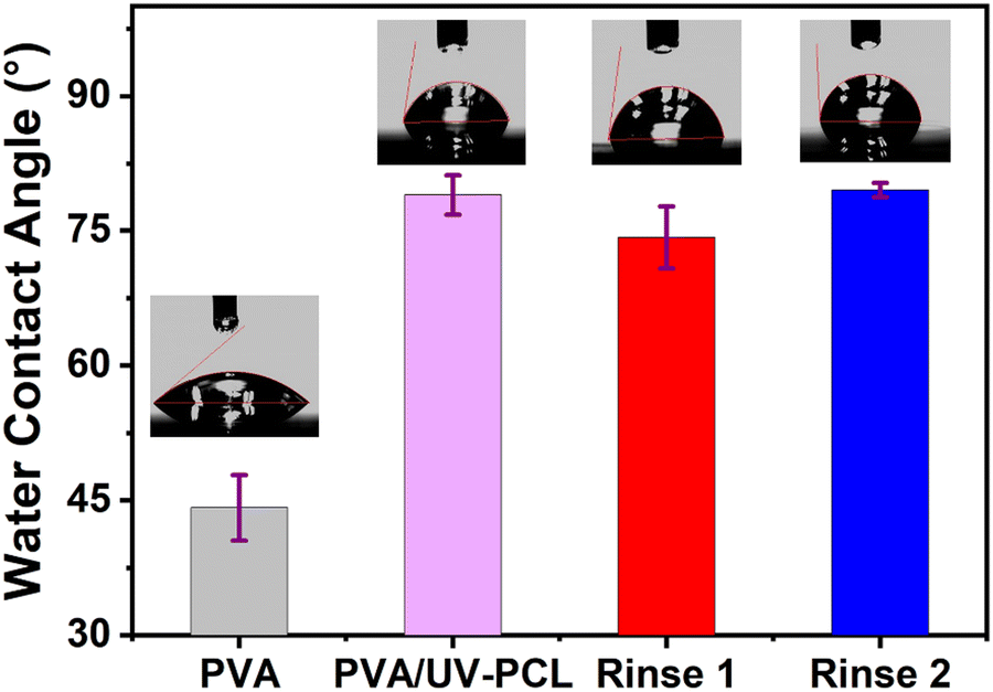 | ||
| Fig. 3 Contact angle measurements for neat PVA and PVA/UV-PCL. | ||
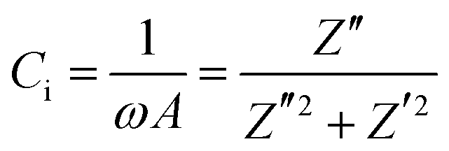
The dielectric properties of the bilayer dielectric (PVA/UV-PCL) were characterized by impedance spectroscopy and are summarized in Table 1. The bilayer dielectric constant values found were well within the predicted range for PVA.23,30,68 It has been reported that hygroscopic polymer dielectrics when exposed to moisture can experience an increase in the capacitance density by up to 50 times at 10 Hz.27 This change is explained by the fact that moisture acts as a plasticizer, facilitating hydroxyl group alignment under an applied electric field and thereby increasing the capacitance of the PVA film.69,70 However, for reliable transistors in flexible circuits, the dielectric properties need to be stable. Water molecules also introduce charge traps at the dielectric–semiconductor interface, increasing the device hysteresis which is also detrimental to the transistor performance. Therefore, a monolayer (∼1–2 nm) of UV-cross-linkable PCL layer deposited on top of PVA functions as a moisture barrier, thereby reducing the impact of moisture on the dielectric properties of PVA.27
| Dielectric | Effective dielectric constant (k) | Capacitance density (nF cm−2) |
|---|---|---|
| PVA/UV-PCL | 10.6 ± 1.6 | 26.70 ± 0.04 |
F10-SiPc was deposited on the UV-PCL layer. F10-SiPc OTFTs using OTS-treated SiO2 as the gate dielectric were fabricated using a similar device configuration for device performance comparison.23,27,30,68–70 Finally Cr and then Au were deposited on the semiconductor as the source/drain electrodes using shadow masks. The Cr interlayer improves electrode durability71 and reduce contact resistance by matching the work function of the electrode with the lower unoccupied molecular orbital (LUMO) energy level of F10-SiPc.72,73
Fig. 4a–d depicts the characteristic output and transfer curves of the F10-SiPc OTFTs on both PVA/UV-PCL and OTS-treated SiO2 dielectrics. The VT, electron mobility (μe) and on/off current (Ion/off) were determined and are presented in Table 2. The VT value of F10-SiPc OTFTs was reduced noticeably from 12.7 ± 1.7 V when using OTS-treated SiO2 as the gate dielectric to −0.97 ± 1.4 V when using a PVA/UV-PCL bilayer as the gate dielectric. The decrease in VT implies a reduction in polarity at the semiconductor/dielectric interface, minimizing the amount of charge trapping,29,74–76 which is likely due to the higher dielectric constant of PVA/UV-PCL (10.6) compared to SiO2 (3.9), at frequencies below 1 kHz.77 This represents a significant improvement compared to previous studies53 where biocompatible and bioresorbable OTFTs were fabricated utilizing PVA as the gate dielectric with VT values of approximately −15.4 V. A statistically similar μe was observed, going from (2 ± 0.7) × 10−2 cm2 V−1 s−1 on the OTS/SiO2 gate dielectric to (1.03 ± 1.6) × 10−2 cm2 V−1 s−1 when PVA/UV-PCL was used. This is consistent with previous research on bottom-gate devices that include the deposition of F10-SiPc on the PMMA dielectric, which provided an electron mobility of 1.1 × 10⁻² cm2 V−1 s−1, lower than that obtained with F10-SiPc deposited on SiO2.52 Although the Ion/off ratios are comparatively low, this aligns with the literature reported for PVA dielectrics.78 The high off current observed in Fig. 4d might be due to the ambipolarity of the device as F10-SiPc has been demonstrated as an ambipolar semiconducting material. It is important to note that devices prepared on OTS/SiO2 had higher currents than devices prepared on PVA/UV-PCL which is a function of several factors including the operating conditions used to obtain the transfer and output curves, which are different in terms of VGS and VSD. With PVA/UV-PCL devices tested at VGS and VSD = 4 V, we obtain a current of ≈0.073 μA, but when using OTS/SiO2 at the same VGS and VSD the device does not turn on, highlighting the low voltage requirements when using PVA/UV-PCL. A comparable current is only obtained at ∼25 V when using OTS/SiO2.
 | ||
| Fig. 4 Output curves of (a) SiO2/OTS and (b) PVA/UV-PCL, and transfer curves of (c) OTFT on OTS treated SiO2 and (d) on PVA/UV-PCL. The transfer characteristics curve versus VGS were obtained for VSD = 50 V and VSD = 3 V, respectively. 1D XRD pattern for F10-SiPc on (e) OTS treated SiO2 and (f) on the PVA-UV-PCL dielectric. | ||
| Dielectric | μ e (cm2 V−1 s−1) | V T (V) | I on/off |
|---|---|---|---|
| SiO2/OTS | 0.02 ± 0.007 | 12.7 ± 1.7 | 105 (at VGS = 50 V) |
| PVA/UV-PCL | 0.01 ± 0.016 | −0.97 ± 1.4 | 101–102 (at VGS = 4 V) |
Enhanced crystallinity in MPcs deposited by physical vapour deposition (PVD) generally results in enhanced charge transport characteristics in OTFTs, leading to greater mobility and on-current values, while amorphous MPcs typically show higher numbers of defect sites, which decreases the conductivity and mobility of the semiconductor.79 The crystallization of MPcs is impacted by substrate characteristics, molecular order of the sub-layer, surface roughness, chemistry, and deposition rate.80,81Fig. 4e and f show a comparison of XRD patterns of F10-SiPc films deposited on OTS-treated SiO2 and the PVA/UV-PCL dielectric. A reduction in peak intensity at 2θ = 8.43° for F10-SiPc films deposited on PVA/UV-PCL was observed compared to those on the OTS-treated SiO2 surface which might result in a change in relative crystallinity, change in polymorph or change in crystalline domain orientation. This discrepancy can be attributed to the differing surface diffusion behaviour of F10-SiPc molecules on PVA/UV-PCL compared to OTS-treated SiO2 during the nucleation of F10-SiPc vapours on the substrate and is consistent with the observed slight drop in device μe.52 Overall, these results demonstrate that PVA/UV-PCL is an effective green dielectric for the development of R2-SiPc-based OTFTs with a low VT value.
Numerical simulation was carried out to investigate the device physics of the corresponding transistors.82–84 We determined a set of models and parameters that reproduce the major characteristics of the OTFT based on the SiO2/OTS dielectric including both bulk traps and fixed charge at the semiconductor/insulator interface as shown in Fig. 5a. It is worth mentioning that we will focus on the ON-state simulation data because the simulation returns purely theoretically achievable OFF currents that are typically orders-of-magnitude lower than those realistically measurable. We then took a step-by-step approach to modelling the OTFT based on the PVA/UV-PCL dielectric to identify an origin for the different behaviors of the two transistors. First, we increased the capacitance from 15 nF cm−2 (SiO2/OTS) to 27 nF cm−2 (PVA/UV-PCL), without changing any other material parameters (curve “1”). This simple transformation is not enough to reflect the experimental data, especially because the VT is still too high. Next, to reduce VT, we removed the interface charge, obtaining curve “2”. Finally, we removed the trap states, obtaining curve “3”, which shows an excellent agreement between experiment and simulation, in terms of both the VT and the ON-state current levels. A detailed list of parameters used for the optimized simulation curves in Fig. 5a and b can be found in Table S1, ESI.†
 | ||
| Fig. 5 Comparison between experimentally measured and numerically simulated transfer curves of the OTFT based on (a) SiO2/OTS and (b) PVA/UV-PCL dielectrics. Electron density (n) distribution on a log scale showing (c) channel formation and (d) pinch-off achieved by a low voltage in the OTFT based on the PVA/UV-PCL dielectric. | ||
Our simulation reveals that PVA/UV-PCL does not only offer a large capacitance but it also creates a charge-neutral and trap-minimized surface to enable low-voltage switching. Note that simple conversion of the subthreshold slope to the trap density would lead to the values of 3.5 × 1012 cm−2 eV−1 and 3.3 × 1012 cm−2 eV−1 for the transistors on SiO2 and the polymer bilayer dielectric, respectively. The value for the SiO2 based OTFT may reflect the actual trap density of states (DOS) in this device probed using numerical simulation (Table S1, ESI†). However, this method is likely to overestimate the trap density in the PVA/UV-PLC based OTFT as the subthreshold slope in this sample is not only determined by trap filling but also affected by leakage currents. To further emphasize this argument, we calculated the internal distribution of electrons in the PVA/UV-PCL based OTFT. Fig. 5c shows strongly depleted source/drain regions due to an injection barrier of 0.5 eV, yet the electron accumulation is clearly visible at the semiconductor/insulator interface at a VGS value of only 4 V. Fig. 5d shows that by increasing the VSD value from 0 to 4 V, this channel is successfully pinched-off at the drain side.
We demonstrated that these devices are capable of undergoing degradation under aqueous conditions. PLA resorption is influenced by temperature and pH, and degradation occurs slowly in phosphate buffer saline (PBS) with a pH of 7.4 at room temperature.85 To investigate the resorption behaviour of the device, an accelerated in vitro degradation experiment was performed by immersing the OTFTs in a PBS solution (1 M, pH ∼ 10) at room temperature. The accelerated degradation test demonstrates the complete disintegration of the device in 20 days (Fig. 6). We noticed that the PVA readily dissolved in PBS, and R2-SiPc completely disintegrated from the device within 5 hours. Afterward, a loss of structural integrity was seen, leaving PLA and gold. After 20 days, the whole device was disintegrated completely, leaving micro/nano gold particles in the PBS solution which are known to be excreted or absorbed by the human body.86
 | ||
| Fig. 6 Photographs of OTFTs taken at different intervals after being submerged in 1 M PBS (pH ∼ 10) for accelerated degradation. | ||
We also investigated whether the degradation products obtained from the incubation of OTFT devices in an aqueous medium elicit cytotoxicity in mammalian cells. Degradation product extracts were prepared by incubating devices in culture medium at 37 °C for 7 days following a protocol modified from that in the study by Deng et al.87 The metabolic activity of NIH 3T3 mouse fibroblast cultures following 24 hour incubation with these (OTFT) extracts was not significantly different from that of cultures incubated in fresh medium without the degradation products, whereby metabolic activity is an accepted metric for evaluating cell viability (Fig. 7a). The cells cultured in the presence and absence of degradation products were also incubated with calcein-AM to label live cells (green fluorescence) and ethidium homodimer-1 to label dead cells (red fluorescence). Fluorescence images show the presence of only a few dead cells under both culture conditions, confirming results from the metabolic activity assay (Fig. 7b and c). Overall, these preliminary cell viability studies suggest that the use of UV-PCL, F10-SiPc, Au electrodes, thiol treatment and PLA as a substrate do not cause cytotoxicity to mammalian fibroblasts following degradation of the OTFT devices in aqueous solutions.
 | ||
| Fig. 7 (a) Metabolic activity of NIH 3T3 mouse fibroblasts following 24 hour incubation with degradation product extracts resulting from the incubation of OTFTs in culture medium for 7 days compared to incubation with fresh medium free of the degradation products, and (b) and (c) representative fluorescence images of the cells cultured with (b) and without (c) the degradation products and incubated with calcein-AM to label live cells (green fluorescence) and ethidium homodimer-1 to label dead cells (red fluorescence). | ||
Conclusions
Biocompatible and degradable organic transistors were presented utilizing a water-soluble polymer gate dielectric (PVA) and biodegradable substrate (PLA). The use of a PCL and PVA bilayer gate dielectric effectively lowered the VT value of the R2-SiPc n-type OTFT from 12.7 V to −0.97 V. Processing of the PLA device is critical for appropriate device function, including controlling the annealing conditions of the dielectric to avoid detrimental film roughening and thiol treating the gate for appropriate dielectric coating of the gate. Accelerated bio-disposability of OTFTs was shown by the successful disintegration of the developed devices in the PBS solution within 20 days. Cell viability assays were performed demonstrating negligible cell death and the absence of apparent cytotoxicity for the degradation products of OTFT devices. Owing to their non-toxic, biodegradable nature and low voltage performance, these devices show great promise for next generation environmentally friendly electronics and can minimize the effects of e-waste on the environment and ecosystem.Experimental section
Materials
All chemicals were obtained from Sigma-Aldrich and utilized as received unless otherwise specified. Octyltrichlorosilane (OTS) (97%) was diluted with toluene (anhydrous, 99.8%) to form a 1% v/v solution in a glovebox. PCL diol (Mw = 2000 Da), toluene-2,4-diisocyanate (95%), PLA (230 kg mol−1), PVA (Mw = 31![[thin space (1/6-em)]](https://www.rsc.org/images/entities/char_2009.gif) 000–50000 Da; 98–99% hydrolyzed) and 2-aminoethanthiol hydrochloride were procured from Sigma-Aldrich. Chromium-coated (Cr) tungsten rods and gold (Au, 99.99%) were obtained from Angstrom Engineering. Quartz-coated glass substrates measuring 15 × 20 mm2 were purchased from Ossila Limited. Si wafers with a SiO2 thickness of 230 nm and shadow masks were obtained from WaferPro and Ossila Limited, respectively. Deuterated chloroform, with a purity of 99.8%, and benzene, with a purity of 98%, were acquired from Cambridge Isotope Laboratories Inc. The synthesis of F10-SiPc was carried out according to the literature.88 2,2-Dimethyl benzodioxinone-terminated PCL (UV-PCL) was synthesized according to the literature.27
000–50000 Da; 98–99% hydrolyzed) and 2-aminoethanthiol hydrochloride were procured from Sigma-Aldrich. Chromium-coated (Cr) tungsten rods and gold (Au, 99.99%) were obtained from Angstrom Engineering. Quartz-coated glass substrates measuring 15 × 20 mm2 were purchased from Ossila Limited. Si wafers with a SiO2 thickness of 230 nm and shadow masks were obtained from WaferPro and Ossila Limited, respectively. Deuterated chloroform, with a purity of 99.8%, and benzene, with a purity of 98%, were acquired from Cambridge Isotope Laboratories Inc. The synthesis of F10-SiPc was carried out according to the literature.88 2,2-Dimethyl benzodioxinone-terminated PCL (UV-PCL) was synthesized according to the literature.27
Preparation of a self-assembled monolayer solution
A solution of a self-assembled monolayer of hydrophilic thiols was prepared by dissolving 10 mM 2-aminoethanethiol hydrochloride in an ethanol solvent.Preparation of the substrate and dielectric
PLA was selected to be used as a biodegradable substrate for the fabrication of OTFTs. A PLA solution of 80 mg ml−1 was prepared by dissolving granules of PLA (230 kg mol−1) in a chloroform solvent followed by filtering with 0.45-micron PTFE filters. The PVA solution was prepared by dissolving 80 mg of PVA in 1 ml of distilled water and then filtering it through a 0.45 μm cellulose filter. Next, UV-PCL was weighted and transferred into an opaque vial, where it was dissolved in toluene to obtain a concentration of 2 mg ml−1. Afterwards, the vial containing UV-PCL was left on a hot plate set at 60 °C for 1 hour to guarantee full dissolution. The UV-PCL solution obtained was subsequently passed through a 0.22 μm PTFE filter into a separate opaque vial. These procedures were conducted under ambient conditions.Fabrication of TFT
OTFTs were fabricated using a quartz-coated glass substrate (15 × 20 mm2). The quartz substrates were used as temporary substrates. The substrates were cleaned using a four-step method. The substrates were first sonicated for five minutes by sequentially immersing them in detergent mixed with distilled water, distilled water, acetone, and methanol. Then, the substrates were rinsed with isopropanol and dried using a nitrogen stream. The PLA solution was then spin-coated at 2000 rpm for 90 seconds on glass substrates using a Laurell WS-650-23 spin coater. Subsequently, the PLA-coated glass substrates were vacuum annealed at 70 °C for 15 minutes. After baking the film of PLA, a film of ∼3–4 microns was obtained. Next, using a shadow mask and the physical vapor deposition (PVD) method, a 2 nm layer of Cr (deposited at a rate of 0.5 Å s−1) and a 50 nm layer of gold (deposited at a rate of 0.5 Å s−1) were deposited on to the PLA substrate. Then, PLA substrates coated with gold were immersed in a hydrophilic thiol solution for one hour to form a self-assembled monolayer of thiols. The purpose of this monolayer is to enhance the hydrophilicity of the gold layer on PLA. Next, a solution of PVA (80 mg ml−1) was spin-coated on gate electrode coated PLA substrate at 2000 rpm for 90 s followed by annealing at 50 °C for overnight to ensure that the PVA film was dried well. Afterwards, a 2 mg ml−1 solution of UV-PCL was deposited on the PVA dielectric layer using spin coating at 2000 rpm for 90 s. The spin coated UV-PCL on the PVA dielectric film was crosslinked using an ultraviolet (UV) lamp with a wavelength of 254 nm. After that, the samples were transferred to a nitrogen glovebox connected to a thermal evaporator. The F10-SiPc layer was thermally deposited by a PVD method, forming a 500 Å-thick film of F10-SiPc using a square shadow mask. During the deposition procedure, the substrates were kept at room temperature, and the process was carried out at a rate of 0.2 Å s−1 under a pressure of less than 2 × 10⁻⁶ torr. Then, using a shadow mask, a 2 nm layer of chromium (deposited at a rate of 0.5 Å s−1) and a 50 nm layer of gold (deposited at a rate of 0.5 Å s−1) were deposited to obtain source–drain electrodes with dimensions of L = 30 μm and W = 1000 μm. A similar architecture was used for the fabrication of OTFTs with SiO2 serving as the gate dielectric. SiO2/Si wafers were first cleaned using the same cleaning process, and then they were treated with oxygen plasma for 15 minutes. To create a monolayer of OTS on the SiO2 surfaces, the wafers were then immersed in a 1% v/v OTS solution in toluene for an hour at 70 °C. They were then rinsed with toluene and dried in a vacuum oven at 70 °C. Following surface treatment, the substrates were placed in a glovebox and a 50 nm layer of F10-SiPc was deposited. Next, Cr–Au source–drain electrodes were deposited using similar settings to those previously mentioned.Device characterization
The OTFT devices were tested in a N2 glovebox utilizing a custom-built auto tester62 that was connected to a Keithley 2614B instrument. This configuration facilitated the control of the voltage between the source and drain (VSD) and the voltage between the source and gate (VGS), as well as the measurement of the current flowing between the source and drain (ISD) in OTFTs. The output curves were obtained by sweeping the source–drain voltage (VSD) from 0 to 4 V, while the gate–source voltage (VGS) varied from −3 to 4 V. The transfer curves were obtained by setting VSD = 3 V for biodegradable polymer-gated OTFTs and 50 V for SiO2-gated OTFTs. VGS was then varied from −3 to 4 V for biodegradable polymer-gated devices and from 0 to 50 V for SiO2-gated devices. The values of electron mobility (μe), threshold voltage (VT), and on/off current ratio (Ion/off) were computed by examining the transfer curves in the saturation regime which are modelled utilizing eqn (1):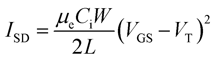 | (1) |
 | (2) |
Thin film characterization
Bruker D8 Endeavour apparatus was used to record the X-ray diffraction (XRD) patterns of 50 nm thick F10-SiPc films on a SiO2 dielectric treated with OTS, as well as a biodegradable bilayer dielectric (PVA/UV-PCL). Cu Kα radiation (λ = 1.5418 Å) was used, and the scan rate was set to 0.5° min−1, covering a range of 7° < 2θ < 14°.Furthermore, each polymer film was subjected to a contact angle measurement (θ) with deionized (DI) water. This was obtained by dispensing 0.5 μl droplets of each reference liquid and taking an image of the drops with a VCA Optima goniometer camera (AST Products Inc.).
A Bruker Dektak XT profilometer was used to measure the dielectric layer thickness and roughness of the gate electrode surface. The thickness values were then used to correct the mobilities that were measured.
Numerical simulation
A physically based two-dimensional (2D) finite-element numerical solver was used for the simulation of OTFTs (ATLAS, Silvaco). Poisson's equation is solved on a 2D coordinate system to relate the potential variation to the space charge density,| div(εs∇φ) = −ρ | (3) |
 | (4) |
 | (5) |
 and
and  are the electron and hole current density vectors, respectively,
 ![[E with combining right harpoon above (vector)]](https://www.rsc.org/images/entities/i_char_0045_20d1.gif) is the electric field vector, μn and μp are the electron and hole mobility, respectively, Dn and Dp are the electron and hole diffusion coefficients, respectively, q is the elementary charge, n and p are the electron and hole concentrations, respectively. The simulator self-consistently solves eqn (3)–(5) over a 2D mesh that is defined to mimic the cross-section of a fabricated device. The two major outcomes of this process are geometric solutions of the electrostatic parameters and terminal current–voltage characteristics representing the integration of current densities under different bias conditions. An exponential trap DOS at the LUMO edge and a fixed interface charge density were added for the simulation of an OTFT with SiO2/OTS. The functional form of trap DOS is
is the electric field vector, μn and μp are the electron and hole mobility, respectively, Dn and Dp are the electron and hole diffusion coefficients, respectively, q is the elementary charge, n and p are the electron and hole concentrations, respectively. The simulator self-consistently solves eqn (3)–(5) over a 2D mesh that is defined to mimic the cross-section of a fabricated device. The two major outcomes of this process are geometric solutions of the electrostatic parameters and terminal current–voltage characteristics representing the integration of current densities under different bias conditions. An exponential trap DOS at the LUMO edge and a fixed interface charge density were added for the simulation of an OTFT with SiO2/OTS. The functional form of trap DOS is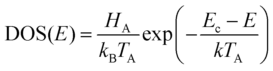 | (6) |
Cytotoxicity evaluation
The cytotoxicity of degradation products from the incubation of OTFT devices in a culture medium was carried out according to a protocol modified from the study by Deng et al.87 Briefly, devices (15 × 20 mm2) were sterilized by incubation in 70% ethanol for 10 minutes, rinsed twice in PBS and incubated in 1 ml of high glucose Dulbecco's modified Eagle's medium (DMEM) for 7 days at 37 °C. The media samples comprising degradation products were then supplemented with fetal bovine serum (FBS) to a final concentration of 10% v/v before being used for cell experiments as degradation product extracts. NIH 3T3 mouse fibroblasts were seeded in DMEM supplemented with 10% FBS at a density of 10000 cells per well in a 48 well plate and allowed to attach for 24 hours in an incubator at 37 °C in an environment characterized by 5% CO2 and 95% relative humidity. Subsequently, the medium was replaced with the degradation product extracts or fresh medium (control) and incubated for an additional 24 hours. Select cultures were evaluated for the metabolic activity of the cells with an alamarBlue assay (Thermo Fisher Scientific), according to the manufacturer's instructions. Additional cultures were incubated with 2 μM calcein AM (Invitrogen; live cell staining; green fluorescence) and 4 μM ethidium homodimer-1 (Sigma Aldrich; dead cell staining; red fluorescence) in DMEM for 10 minutes and imaged using a Zeiss Axio Observer 7 microscope. The degradation products from 5 OTFT devices were tested for both cell viability assays.
Data availability
The data supporting this article have been included as part of the ESI.†Conflicts of interest
There are no conflicts to declare.Acknowledgements
The authors would like to thank the National Science and Engineering Research Council of Canada (NSERC), Canada Research Chair (CRC) program and the Canadian Foundation for Innovation (CFI) for funding this work.References
- V. Murthy and S. Ramakrishna, Sustainability, 2022, 14, 647 CrossRef.
- Y. Khan, A. Thielens, S. Muin, J. Ting, C. Baumbauer and A. C. Arias, Adv. Mater., 2020, 32, 1905279 CrossRef.
- J. Wiklund, A. Karakoç, T. Palko, H. Yiğitler, K. Ruttik, R. Jäntti and J. Paltakari, J. Manuf. Mater. Process., 2021, 5, 89 Search PubMed.
- A. Kumar, M. Holuszko and D. C. R. Espinosa, Resour., Conserv. Recycl., 2017, 122, 32 CrossRef.
- M. J. Tan, C. Owh, P. L. Chee, A. K. K. Kyaw, D. Kai and X. J. Loh, J. Mater. Chem. C, 2016, 4, 5531 RSC.
- S. Hwang, G. Park, H. Cheng, J. Song, S. Kang, L. Yin, J. Kim, F. G. Omenetto, Y. Huang and K. Lee, Adv. Mater., 2014, 26, 1992 CrossRef.
- S.-W. Hwang, H. Tao, D.-H. Kim, H. Cheng, J.-K. Song, E. Rill, M. A. Brenckle, B. Panilaitis, S. M. Won and Y.-S. Kim, Science, 2012, 337, 1640 CrossRef PubMed.
- Y. Ma, Y. Zhang, S. Cai, Z. Han, X. Liu, F. Wang, Y. Cao, Z. Wang, H. Li and Y. Chen, Adv. Mater., 2020, 32, 1902062 CrossRef PubMed.
- K. Liu, B. Ouyang, X. Guo, Y. Guo and Y. Liu, npj Flexible Electron., 2022, 6, 1 CrossRef.
- S. Chatterjee and S. Sharma, F. Actions Sci. Reports. J. F. Actions, 2019, p. 54 Search PubMed.
- P. Wang, M. Hu, H. Wang, Z. Chen, Y. Feng, J. Wang, W. Ling and Y. Huang, Adv. Sci., 2020, 7, 2001116 CrossRef PubMed.
- M. Irimia-Vladu, E. D. Głowacki, G. Voss, S. Bauer and N. S. Sariciftci, Mater. Today, 2012, 15, 340 CrossRef.
- M. A. Loi, E. Da Como, F. Dinelli, M. Murgia, R. Zamboni, F. Biscarini and M. Muccini, Nat. Mater., 2005, 4, 81 CrossRef CAS.
- M. Kaltenbrunner, T. Sekitani, J. Reeder, T. Yokota, K. Kuribara, T. Tokuhara, M. Drack, R. Schwödiauer, I. Graz and S. Bauer-Gogonea, Nature, 2013, 499, 458 CrossRef CAS PubMed.
- T. Sekitani, H. Nakajima, H. Maeda, T. Fukushima, T. Aida, K. Hata and T. Someya, Nat. Mater., 2009, 8, 494 CrossRef CAS PubMed.
- B. C.-K. Tee, A. Chortos, A. Berndt, A. K. Nguyen, A. Tom, A. McGuire, Z. C. Lin, K. Tien, W.-G. Bae and H. Wang, Science, 2015, 350, 313 CrossRef CAS PubMed.
- H. Klauk, U. Zschieschang, J. Pflaum and M. Halik, Nature, 2007, 445, 745 CrossRef CAS.
- Z. B. Henson, K. Müllen and G. C. Bazan, Nat. Chem., 2012, 4, 699 CrossRef CAS.
- C. L. Reichert, E. Bugnicourt, M.-B. Coltelli, P. Cinelli, A. Lazzeri, I. Canesi, F. Braca, B. M. Martínez, R. Alonso and L. Agostinis, Polymers, 2020, 12, 1558 CrossRef CAS.
- E. Chiellini, A. Corti, S. D’Antone and R. Solaro, Prog. Polym. Sci., 2003, 28, 963 CrossRef.
- M. N. Tousignant, V. Tischler, K. Wagner, Z. S. Lin, J. Brusso, R. Izquierdo and B. Lessard, Flexible Printed Electron., 2024, 9, 015012 CrossRef.
- J. Li, W. Tang, Q. Wang, W. Sun, Q. Zhang, X. Guo, X. Wang and F. Yan, Mater. Sci. Eng., R, 2018, 127, 1 CrossRef.
- E. A. Van Etten, E. S. Ximenes, L. T. Tarasconi, I. T. S. Garcia, M. M. C. Forte and H. Boudinov, Thin Solid Films, 2014, 568, 111 CrossRef.
- M. N. Tousignant, N. A. Rice, A. Peltekoff, C. Sundaresan, C. Miao, W. Y. Hamad and B. H. Lessard, Langmuir, 2020, 36, 3550 CrossRef PubMed.
- S. H. Jin, J. S. Yu, J. W. Kim, C. A. Lee, B. Park, J. D. Lee and J. H. Lee, SID Symp. Dig. Tech. Pap., 2003, 34, 1088–1091 CrossRef.
- S. H. Jin, J. S. Yu, C. A. Lee, J. W. Kim, B.-G. Park and J. D. Lee, J. Korean Phys. Soc., 2004, 44, 181 Search PubMed.
- M. N. Tousignant, Z. S. Lin, J. Brusso and B. H. Lessard, ACS Appl. Mater. Interfaces, 2023, 15, 3680 CrossRef PubMed.
- B. R. Teja Karri and N. Gupta, Bull. Mater. Sci., 2019, 42, 2 CrossRef.
- H. Zhang, F. Zhang, J. Sun, M. Zhang, Y. Hu, Z. Lou, Y. Hou and F. Teng, Appl. Surf. Sci., 2019, 478, 699 CrossRef.
- N. V. V. Subbarao, S. Mandal, M. Gedda, P. K. Iyer and D. K. Goswami, Sens. Actuators, A, 2018, 269, 491 CrossRef.
- X.-J. She, J. Liu, J.-Y. Zhang, X. Gao and S.-D. Wang, Appl. Phys. Lett., 2013, 103 Search PubMed.
- C. Rullyani, M. Ramesh, C.-F. Sung, H.-C. Lin and C.-W. Chu, Org. Electron., 2018, 54, 154 CrossRef.
- C. Pang, N. Neubauer, M. Boyles, D. Brown, N. Kanase, D. Hristozov, T. Fernandes, V. Stone, W. Wohlleben and A. Marcomini, NanoImpact, 2017, 7, 75 CrossRef.
- A. GÜnsel, A. UsluoĞlu, A. T. Bilgicli, B. Tosun, G. Arabaci and M. N. YaraŞir, Turk. J. Chem., 2020, 44, 923 CrossRef.
- L. Nie, G. Chang and R. Li, Coatings, 2020, 10, 741 CrossRef CAS.
- J. Mao, Y. Zhang, J. Zhu, C. Zhang and Z. Guo, Chem. Commun., 2009, 908 RSC.
- K. Mitra, M. Samsó, C. E. Lyons and M. C. T. Hartman, J. Mater. Chem. B, 2018, 6, 7373 RSC.
- K. Li, W. Dong, Q. Liu, G. Lv, M. Xie, X. Sun, L. Qiu and J. Lin, J. Photochem. Photobiol., B, 2019, 190, 1 CrossRef PubMed.
- M. Mitsunaga, M. Ogawa, N. Kosaka, L. T. Rosenblum, P. L. Choyke and H. Kobayashi, Nat. Med., 2011, 17, 1685 CrossRef PubMed.
- J. T. F. Lau, P.-C. Lo, X.-J. Jiang, Q. Wang and D. K. P. Ng, J. Med. Chem., 2014, 57, 4088 CrossRef PubMed.
- R. R. Cranston, T. D. Lanosky, R. Ewenike, S. Mckillop, B. King and B. H. Lessard, Small Sci., 2024, 2300350 CrossRef.
- R. R. Cranston, M. C. Vebber, J. Faleiro Berbigier, J. Brusso, T. L. Kelly and B. H. Lessard, Adv. Electron. Mater., 2022, 8, 2200696 CrossRef.
- B. King, M. C. Vebber, R. Ewenike, M. Dupuy, C. French, J. L. Brusso and B. H. Lessard, Chem. Mater., 2023, 35, 8517 CrossRef.
- R. B. Ewenike, B. King, A. M. Battaglia, J. D. Quezada Borja, Z. S. Lin, J. G. Manion, J. L. Brusso, T. L. Kelly, D. S. Seferos and B. H. Lessard, ACS Appl. Electron. Mater., 2023, 5, 7023 CrossRef.
- B. H. Lessard, ACS Appl. Mater. Interfaces, 2021, 13, 31321 CrossRef PubMed.
- S. Brixi, C. L. Radford, M. N. Tousignant, A. J. Peltekoff, J. G. Manion, T. L. Kelly and B. H. Lessard, ACS Appl. Mater. Interfaces, 2022, 14, 40361 CrossRef PubMed.
- F. Torricelli, D. Z. Adrahtas, Z. Bao, M. Berggren, F. Biscarini, A. Bonfiglio, C. A. Bortolotti, C. D. Frisbie, E. Macchia, G. G. Malliaras, I. McCulloch, M. Moser, T.-Q. Nguyen, R. M. Owens, A. Salleo, A. Spanu and L. Torsi, Nat. Rev. Methods Primers, 2021, 1, 66 CrossRef PubMed.
- S. K. Possanner, K. Zojer, P. Pacher, E. Zojer and F. Schürrer, Adv. Funct. Mater., 2009, 19, 958 CrossRef.
- M. N. Tousignant, B. Ronnasi, V. Tischler and B. H. Lessard, Adv. Mater. Interfaces, 2023, 10, 2300079 CrossRef CAS.
- M. M. Hasan, M. M. Islam, X. Li, M. He, R. Manley, J. Chang, N. Zhelev, K. Mehrotra and J. Jang, IEEE Trans. Electron Devices, 2020, 67, 1751 CAS.
- G. Konwar, P. Saxena, V. Raghuwanshi, S. Rahi and S. P. Tiwari, ACS Appl. Electron. Mater., 2022, 4, 2525 CrossRef CAS.
- B. Ronnasi, B. King, S. Brixi, S. Swaraj, J. Niskanen and B. H. Lessard, Adv. Electron. Mater., 2024, 2300810 CrossRef CAS.
- C. J. Bettinger and Z. Bao, Adv. Mater., 2010, 22, 651 CrossRef CAS PubMed.
- F. Witte, in Biodegradable Metals, ed. W. R. Wagner, S. E. Sakiyama-Elbert, G. Zhang and M. J. Yaszemski, Academic Press, 2020, pp. 271–287 Search PubMed.
- G. Voskerician, R. S. Shawgo, P. A. Hiltner, J. M. Anderson, M. J. Cima and R. Langer, IEEE Trans. Biomed. Eng., 2004, 51, 627 CrossRef PubMed.
- G. S. Wilson and Y. Hu, Chem. Rev., 2000, 100, 2693 CrossRef CAS PubMed.
- M. Peng, J. Wang, Z. Li, G. Ren, K. Li, C. Gu and Y. Lin, Talanta, 2023, 253, 123891 CrossRef CAS PubMed.
- E. R. Edelman, P. Seifert, A. Groothuis, A. Morss, D. Bornstein and C. Rogers, Circulation, 2001, 103, 429 CrossRef CAS PubMed.
- G. Voskerician, M. S. Shive, R. S. Shawgo, H. Von Recum, J. M. Anderson, M. J. Cima and R. Langer, Biomaterials, 2003, 24, 1959 CrossRef.
- J. R. G. Carvalho, G. Conde, M. L. Antonioli, P. P. Dias, R. O. Vasconcelos, S. R. Taboga, P. A. Canola, M. A. Chinelatto, G. T. Pereira and G. C. Ferraz, Polym. J., 2020, 52, 629 CrossRef.
- C. C. Silva, D. Thomazini, A. G. Pinheiro, N. Aranha, S. D. Figueiro, J. C. Góes and A. S. B. Sombra, Mater. Sci. Eng. B, 2001, 86, 210 CrossRef.
- J. Manion and B. H. Lessard, Nat. Rev. Mater., 2024, 9, 377 CrossRef.
- H. Notsu, W. Kubo, I. Shitanda and T. Tatsuma, J. Mater. Chem., 2005, 15, 1523 RSC.
- J. Kettle and D. Kumar, in 2021 23rd Eur. Microelectron. Packag. Conf. Exhib., IEEE, 2021, pp. 1–4.
- S. B. Kv, A. S. Rama Teja, N. Srinivas Babu, V. Arunachalam, C. V. S. Maheswar and A. Reddy, Res. J. Chem. Sci., 2014, 89–93 Search PubMed.
- M. N. Tousignant, N. A. Rice, J. Niskanen, C. M. Richard, D. Ritaine, A. Adronov and B. H. Lessard, Adv. Electron. Mater., 2021, 7, 2100700 CrossRef.
- G. Grau and V. Subramanian, Flexible Printed Electron., 2020, 5, 14013 CrossRef.
- R. P. Ortiz, A. Facchetti and T. J. Marks, Chem. Rev., 2010, 110, 205 CrossRef.
- E. M. Amin, N. C. Karmakar and B. Winther-Jensen, Prog. Electromagn. Res. B, 2013, 54, 149 CrossRef.
- T. Tsai, J. Chang, T. Wen and T. Guo, Adv. Funct. Mater., 2013, 23, 4206 CrossRef.
- B. Mirka, N. A. Rice, C. M. Richard, D. Lefebvre, B. King, W. J. Bodnaryk, D. Fong, A. Adronov and B. H. Lessard, ACS Appl. Nano Mater., 2022, 5, 12487 CrossRef.
- O. A. Melville, T. M. Grant, K. Lochhead, B. King, R. Ambrose, N. A. Rice, N. T. Boileau, A. J. Peltekoff, M. Tousignant and I. G. Hill, ACS Appl. Electron. Mater., 2020, 2, 1313 CrossRef.
- N. J. Dallaire, S. Brixi, M. Claus, S. Blawid and B. H. Lessard, Appl. Phys. Rev., 2022, 9, 011418 Search PubMed.
- B. Nketia-Yawson and Y. Noh, Adv. Funct. Mater., 2018, 28, 1802201 CrossRef.
- A. Nawaz and I. A. Hümmelgen, J. Mater. Sci.: Mater. Electron., 2019, 30, 5299 CrossRef.
- Y. Sun, Y. Liu, Y. Wang, C. Di, W. Wu and G. Yu, Appl. Phys. A: Mater. Sci. Process., 2009, 95, 777 CrossRef.
- J. Puigdollers, C. Voz, M. Fonrodona, S. Cheylan, M. Stella, J. Andreu, M. Vetter and R. Alcubilla, J. Non-Cryst. Solids, 2006, 352, 1778 CrossRef.
- S. Vasimalla, N. V. V. Subbarao, M. Gedda, D. K. Goswami and P. K. Iyer, ACS Omega, 2017, 2, 2552 CrossRef.
- B. King, C. L. Radford, M. C. Vebber, B. Ronnasi and B. H. Lessard, ACS Appl. Mater. Interfaces, 2023, 15, 14937 CrossRef CAS PubMed.
- R. R. Cranston, B. King, C. Dindault, T. M. Grant, N. A. Rice, C. Tonnelé, L. Muccioli, F. Castet, S. Swaraj and B. H. Lessard, J. Mater. Chem. C, 2022, 10, 485 RSC.
- R. R. Cranston and B. H. Lessard, RSC Adv., 2021, 11, 21716 RSC.
- S.-W. Jo, S. Cho and C.-H. Kim, J. Phys. D: Appl. Phys., 2022, 55, 405101 CrossRef CAS.
- H. Lee, Y. E. Kim, J. Bae, S. Jung, R. A. Sporea and C.-H. Kim, ACS Appl. Mater. Interfaces, 2023, 15, 10918 CrossRef CAS.
- J. Bae, S. Park, H. Jung, E.-H. Ko, I. Kymissis and C.-H. Kim, J. Mater. Sci.: Mater. Electron., 2024, 35, 185 CrossRef CAS.
- M. Ali, S. M. Hoseyni, R. Das, M. Awais, I. Basdogan and L. Beker, Adv. Mater. Technol., 2023, 8, 2300347 CrossRef CAS.
- M. Wu, K. Yao, N. Huang, H. Li, J. Zhou, R. Shi, J. Li, X. Huang, J. Li and H. Jia, Adv. Sci., 2023, 2300504 CrossRef CAS PubMed.
- Y. Deng, H. Qi, Y. Ma, S. Liu, M. Zhao, Z. Guo, Y. Jie, R. Zheng, J. Jing and K. Chen, Proc. Natl. Acad. Sci. U. S. A., 2022, 119, e2208060119 CrossRef CAS.
- O. A. Melville, T. M. Grant and B. H. Lessard, J. Mater. Chem. C, 2018, 6, 5482 RSC.
Footnote |
| † Electronic supplementary information (ESI) available. See DOI: https://doi.org/10.1039/d4ma01148a |
| This journal is © The Royal Society of Chemistry 2025 |