
 Open Access Article
 This Open Access Article is licensed under a Creative Commons Attribution-Non Commercial 3.0 Unported Licence
Tuning of the structural and electrical properties of thermo-luminescent tungsten-doped indium oxide thin film
Aparna
C.
,
Pramoda Kumara
Shetty
 * and
Mahesha
M. G.
* and
Mahesha
M. G.
Department of Physics, Manipal Institute of Technology, Manipal Academy of Higher Education, Manipal 576104, India. E-mail: pramod.shetty@manipal.edu
First published on 12th December 2024
Abstract
This paper aims to synthesize tungsten-doped indium oxide thin film and to study its properties. Films with different tungsten dopant concentrations were deposited using the technique of spray pyrolysis. Raman spectroscopy and X-ray diffraction were used to investigate the structural features. It confirms the polycrystalline cubic structure of W-doped indium oxide. The morphological change observed with doping supports the preferred plane orientation change. Optical properties were studied using UV-visible spectroscopy. The photoluminescence spectra showed both near-band emission (NBE) and violet-blue emission. The suitability of the material for gamma sensing applications was confirmed by thermoluminescence (TL) spectroscopy. The binding energy obtained from the core XPS spectra of W corresponds to a 6+ oxidation state. The electrical resistivity decreased with tungsten doping and it is attributed to the increase in donor electrons. Indium oxide doped with 2 at% W has good structural, optical, and electrical characteristics that make it suitable for use in sensor applications.
1. Introduction
Transparent conducting oxides (TCOs) have garnered significant attention from researchers in recent times because of their exceptional capabilities and extensive use in optoelectronic applications, including resistive memory devices, touch panels, photovoltaics, light-emitting diodes, and flat panel displays.1 Among different TCOs, indium oxide (InO) has drawn a lot of interest recently in the field of semiconductors because of its potential qualities. In2O3 is a wide bandgap semiconductor with good electrical conductivity, better stability and high transparency.2 InO thin films are of great interest in various applications, including gas sensors, photovoltaics, transparent conductive electrodes, and gamma sensors.3 Because of its great sensitivity, affordability, and ability to be miniaturized, thin films of metal oxides are advantageous in gamma sensors and can be employed in wearable and portable dosimeters.4 The material's response to gamma radiation involves changes in its electrical and optical characteristics, which can be measured to estimate radiation dose.In metal oxides, doping is the intentional incorporation of impurities, usually in trace amounts, to change the material's characteristics. Metal oxide thin films can be doped to improve their performance for a variety of uses. Doping metal oxide thin films can increase their sensitivity to ionising radiation, particularly gamma rays, in the context of gamma dosimetry.5 InO can be doped with a broad range of elements to satisfy the requirements of numerous application domains. According to reports, doping indium oxide with molybdenum enhanced its electrical properties and transparency. The significant valence disparity between dopant ions and substituting indium ions is thought to be the cause of the reported improvement.6 In line with this idea of doping high valence difference ions into In2O3, we synthesised tungsten-doped indium oxide (IWO) films using spray pyrolysis. The requirements of the application and the desired material qualities determine the dopant and doping concentration to be used. Doping with transition metal ions like tungsten can add localised energy levels to the metal oxide's bandgap, increasing its gamma radiation sensitivity. Doping can be accomplished in several ways when preparing metal oxide films, including co-deposition, ion implantation, and post-deposition annealing in an environment that contains dopants.
Numerous deposition techniques, such as spin coating, magnetron sputtering, pulsed laser deposition (PLD) and spray pyrolysis, are used to create InO thin films.2,7–9 Spray pyrolysis is regarded as a good approach among the methods used to create InO films because of its inherent simplicity in usage and is economical.9 The most common method used to create tungsten-doped InO films documented in the literature is sputtering. We report on the synthesis and characterisation of tungsten-doped InO thin film in this communication. W-doped InO films have been made using a solution-based method, which offers greater control over the dopant concentration in the film than does the vacuum-based method.1
Few studies have been reported on tungsten-doped indium oxide but no studies were done on it for low-dose gamma sensing applications.1,10 This work mainly focuses on optimizing the tungsten doping concentration in indium oxide thin film for low-dose gamma sensor applications. Also, this study examined and described how the tungsten doping content affected the structural, optical, electrical and spectroscopic characteristics of IWO films. Furthermore, there has been no research done so far on the thermoluminescent properties of indium oxide doped with tungsten.
2. Experimental details
Nanostructured IWO with dopant concentration varied from 2–10 at% were synthesized using the low-cost spray pyrolysis method on a glass substrate. The glass substrates (dimensions: 2.5 cm × 2.5 cm) were prepared by sequential cleaning: first in a water bath with ultrasonication, followed by treatments with HCl, isopropyl alcohol (IPA), and acetone. The doped films were deposited onto the microscopic glass substrates at an optimized substrate temperature of 450 °C with 0.1 M precursor solution. For the precursor solution, indium chloride tetrahydrate (InCl3·4H2O) was dissolved in 10 ml of distilled water and stirred at room temperature on a magnetic stirrer for 30 minutes. Concurrently, a solution of ammonium tungsten oxide hydrate (the dopant source) was prepared in deionized water and also stirred for 30 minutes. Two solutions of the required amounts were mixed and followed by an additional 15 minutes of stirring to ensure homogeneity. The prepared solution was sprayed onto the preheated glass substrate using a spray pyrolysis unit. Deposition parameters were kept constant as reported in our previous study.11 The thin film's X-ray diffraction spectra were examined using a Rigaku Miniflex-600 X-ray diffractogram using a radiation source of Cu Kα. Surface morphology with composition was studied using a Carl Zeiss 03–81 Sigma FESEM with EDS. LAB RAM HR Horiba France was used to obtain micro Raman spectra using a 532 nm laser. The SHIMADZU UV 1900 spectrophotometer was used to measure the synthesised film's optical response. Using a 325 nm excitation wavelength, the Jasco FP-8300 fluorescence spectrometer was used to capture the photoluminescence spectra of the films at room temperature. Using an Al Kα X-ray source, a PHI 5000 Versa Probe III was used to conduct XPS investigations. The TL measurements were done within a temperature range of 30 °C to 300 °C with a heating rate of 2.7 °C s−1 using a PC-controlled TL reader. Using a Keithley 2450 source meter and the Van der Paw technique, Hall measurements were performed.3. Results and discussion
3.1. Structural properties
The information on the structure and crystallographic phase under the influence of W doping on InO thin film is studied through an X-ray diffractogram. Fig. 1(a) represents the XRD spectra of pure and tungsten-doped indium oxide thin film with a dopant concentration variation from 2 at% to 10 at%. The polycrystallinity of the deposited films with diffraction peaks along the (222), (400), (440) and (622) planes corresponding to pure cubic indium oxide (ICDD: 76-0152) was confirmed using the spectra. It also confirms the absence of undesired phase or impurity peaks indicating the purity of the deposited films. | ||
| Fig. 1 XRD spectra of undoped and W-doped In2O3 films of different dopant concentrations. | ||
The diffraction intensities of the InO thin film significantly changed with the incorporation of W and this is due to electron density variation due to the W atom and ionic radius.12 When the dopant concentration increased from 2 to 6 at%, the intensity ratio of the (400) peaks and (222) peaks of the deposited film increased and beyond that, it started decreasing. The strongest peak corresponds to the (400) plane up to 8 at% of W doping and gradually it started switching to the (222) plane with an increase in dopant concentration. At 10 at% of W, the peak intensity of both planes became more or less the same indicating a preferential orientation change of from (400) to (222). i.e., the preferred orientation of the deposited material changes with dopant concentration. We have already reported a similar orientation change in the InO thin film, which was doped with zinc.13 S. Parthiban et al. reported a shift in preferential orientation from the (222) plane to the (400) plane with Mo doping in the InO thin film.6 Cation incorporation as well as deposition conditions have a great influence on the preferential orientation change. The report of Agashe et al. on sprayed SnO2 states that even the excessive inclusion of the host cation can also change preferred growth. The report also points out that the substitutional dopant incorporation even at regular as well as interstitial sites has no influence on the preferential orientation. Whereas the occupancy of the dopant at previously unoccupied additional interstitial sites can change the preferred growth.14 The higher intensity of the preferred plane of 2 at% doped InO thin film corresponds to the better crystalline quality.15 The diffraction peaks become weaker and broader with an increment in the dopant concentration and this can be due to the paucity of arrangements arising from higher doping levels and also ionic radii differences between the host and dopant. Peak intensity decrement and peak width increment signify crystallinity degradation which could be assigned to the doping-induced lattice disorder and strain.16 Md. A. Sayeed et al. attributed the peak intensity reduction and peak shift to the grain size reduction after the introduction of the dopant.12
The tungsten atom incorporation in the InO lattice can introduce a change in lattice constant or even defect generation, which results in a diffraction peak shift, as illustrated in Fig. 1(b).10 Both the (400) and (222) planes exhibit an anomalous shift in IWO thin film. IWO films with tungsten possessing a lower ionic radius than indium are expected to show a higher angle shift. Whereas we noticed a slight shift of the diffraction peaks of the doped film towards lower angles compared to pristine InO. A lower angle shift with an increase in dopant concentration indicates lattice expansion due to W doping. This shift accounts for the slight increase in the unit cell parameter (a) from 10.11 Å for InO to 10.19 Å for IWO. The high carrier concentration in the conduction band originating from the cationic substitution of tungsten could be correlated to the cell parameter enhancement.17 Arife Gencer Imer et al. attributed the increase of lattice parameter in the Al-doped CdO thin film to the migrating dopant atoms in the grain boundaries.18
The average crystallite size has been evaluated using both the Scherrer equation and the size strain plot (SSP). The size strain plot of the tungsten doped indium oxide thin film with different dopant concentrations is shown in Fig. 2. The compilation of the estimated structural parameters including the average crystallite size is presented in Table 1.
 | ||
| Fig. 2 SSP plot of W-doped In2O3 films of different dopant concentrations (2 at%, 4 at%, 6 at%, 8 at%, 10 at%). | ||
| Sample | Dopant concentration (at%) | Preferred orientation | Crystallite size (nm) | a (Å) | Strain × 10−3 | δ × 1015 lines m−2 | |
|---|---|---|---|---|---|---|---|
| Scherrer formula | SSP | ||||||
| IWO_0 | 0 | (400) | 36.30 ± 0.80 | 29.70 ± 0.50 | 10.11 | 0.98 ± 0.01 | 1.13 ± 0.0419 |
| IWO_2 | 2 | (400) | 24.88 ± 0.23 | 17.98 ± 0.003 | 10.16 | 1.39 ± 0.04 | 3.09 ± 0.001 |
| IWO_4 | 4 | (400) | 22.41 ± 0.18 | 16.08 ± 0.002 | 10.15 | 1.55 ± 0.04 | 3.87 ± 0.0009 |
| IWO_6 | 6 | (400) | 25.60 ± 0.18 | 14.19 ± 0.001 | 10.17 | 1.35 ± 0.03 | 4.97 ± 0.0007 |
| IWO_8 | 8 | (400) | 22.24 ± 0.17 | 14.02 ± 0.001 | 10.18 | 1.56 ± 0.03 | 5.09 ± 0.0007 |
| IWO_10 | 10 | (222) | 14.83 ± 0.12 | 14.55 ± 0.001 | 10.19 | 2.34 ± 0.06 | 4.72 ± 0.0006 |
The crystallite size reduced with the incorporation of dopant in the InO film and it exhibits a decreasing trend with a rise in concentration of dopant. It decreased from 29.70 nm to 14.55 nm with an increment in W concentration from 0 at% to 10 at%. Relatively smaller crystallite size indicates the lower surface roughness of the film after doping.18 The diminution in the crystallinity after doping can be ascribed to the created oxygen vacancies or oxygen interstitials.20
The dislocation density increased with doping concentration, which is attributable to the ionic radii difference of indium and tungsten ions. The 6 at% doped indium oxide seemed to be less strained and can be ascribed to the successful replacement of tungsten in the host matrix.21 The strain value is calculated using the relation reported elsewhere11 and the obtained values are tabulated in Table 1. The micro strain, which has a direct impact on hardness, film strength, elasticity, etc. was found to increase with the increase in W content. This implies the increased lattice mismatch with tungsten doping. The microstrain is capable of creating dislocations in the film.12 The difference in the ionic radii of the host and dopant could be the reason for the induced stress.22
3.2. Morphological studies
Scanning electron micrographs are used to examine the surface morphology of W-doped InO thin films. The thin film morphology is dependent on the synthesis technique and fabrication conditions. Moreover, the surface morphology has a direct influence on the optical and electrical properties of the material.2 The dopant and its concentration also have a role in determining the morphology. Fig. 3 represents the surface morphology of the deposited films with different dopant concentrations. Up to 6 at% of doping we have observed hexagonal grains that can be connected to the polycrystallinity of the sample.23 | ||
| Fig. 3 Micrographs of W-doped In2O3 for W concentrations of (a) 2 at%, (b) 4 at%, (c) 6 at%, (d) 8 at% and (e) 10 at%. | ||
A combination of both pyramidal and hexagonal shapes of uneven size can be observed for the 8 at% doping. This can be an indication of the transition of preferred orientation from (400) to (222). The non-uniformity of the film can be attributed to this difference in particle size. The coexistence of grains with different shapes has been previously reported by S. Parthiban et al. for Mo-doped InO thin film.6 The change of grain shape at 10 at% may be the consequence of the shift in the orientation preference from (400) to (222) plane with an increase in doping level. This result is in line with the XRD data. The grain size decreased drastically for the 10 at% doped sample and such variation in grain size with doping concentration has also been previously reported.5 The grain size shrinkage observed at a doping level of 10 at% can also be ascribed to the change in the preferred orientation.24
The composition of the W-doped InO films was investigated using energy-dispersive X-ray (EDAX) analysis. Fig. 4 represents the EDAX spectrum and elemental mapping of the InO thin film doped with 2 at% of tungsten. EDAX spectra reveal the presence of In, O and W in the deposited films. The peaks of O, In and W found in the EDAX spectra arise from K, L and M shells, respectively. Traces of other elements like Si, Na, etc were observed which is attributed to the substrate.21,22 Cl peaks observed in EDAX spectra can be from initial precursor solutions. The stoichiometry of W-doped indium oxide demands around 60% oxygen, and the lower oxygen content found in the EDAX data confirms the presence of oxygen vacancies. The W incorporation into the indium oxide lattice is confirmed from the EDAX spectra.
 | ||
| Fig. 4 Typical EDAX spectrum of 2 at% W-doped In2O3 and elemental mapping of In, W and O. | ||
3.3. Raman analysis
The oxygen vacancy defect growth can be probed using Raman spectroscopy. The local chemical structure of the InO thin film was investigated using micro-Raman spectroscopy. The room temperature Raman spectra of the tungsten doped InO thin film are shown in Fig. 5. The Raman spectrum consists of five well-indexed peaks observed around 108, 131, 305, 364 and 495 cm−1 and it matches well with the previously reported values of pure cubic InO.20 The deconvoluted Raman peak positions are summarized in Table 2. Even though the cubic InO structure is predicted to exhibit 22 Raman active modes, only 5 Raman modes were observed in the present study.25 The absence of any other additional Raman modes indicates the phase purity of the sample and this result is consistent with the XRD data. | ||
| Fig. 5 Raman spectra of W-doped In2O3 for different Zn concentrations. | ||
| Sample | Peak 1 | Peak 2 | Peak 3 | Peak 4 | Peak 5 |
|---|---|---|---|---|---|
| IWO_0 | 108.22 | 129.29 | 304.67 | — | 494.0619 |
| IWO_2 | 108.52 | 131.65 | 305.70 | 364.43 | 495.23 |
| IWO_4 | 107.29 | 131.99 | 306.07 | — | 496.32 |
| IWO_6 | 106.85 | 131.00 | 304.04 | 360.87 | — |
| IWO_8 | — | 131.05 | 304.17 | 362.48 | — |
| IWO_10 | 106 | 130.76 | 304.81 | 365.01 | 495.77 |
The In–O vibrations present in InO6 octahedrons are represented by the 130 cm−1 peak. The peak at 495 cm−1 can be related to the stretching vibration of octahedrons, whereas 306 cm−1 denotes its bending vibration. A new peak emerged at 364 cm−1 in the spectra due to tungsten incorporation indicating the stretching vibration of In–O–In.25 Almost all peaks observed for pure InO were also observed for tungsten-doped InO. With increasing dopant concentration, the intensity of the Raman peak seems to be decreasing and the width increased. The intensity decrement with W doping can be considered due to the incorporation of dopant into the host lattice. The decrease in peak intensity with an increase in dopant concentration up to 8 at% can be correlated to the crystallite variation and the intensity increment for the higher dose is attributed to the higher oxygen vacancies.26 The In–O–In vibrations are mainly influenced by oxygen vacancies and hence such defects are capable of changing the intensity and peak shifting.25
A shift in frequency was also observed. These observations indicate the difference in local symmetry of InO nanoparticles from the bulk, even though both share the same crystal structure.27 After doping with 2% it can be observed that the peak shifts to higher frequencies. The blue shift of the Raman modes observed is attributed to the vacancies, interstitials and grain boundaries. Oxygen vacancies, in particular, lead to a reduction in bond strength, creating stress in the material and a shift in the vibrational frequencies of certain Raman-active modes. The blue shift due to oxygen vacancies was reported by F. Saeed et al.28 Generally, the red shift or blue shift observed in the Raman spectra characterizes the tensile or compressive stress present in the film.29,30 With an increase in dopant concentration, the Raman spectra show a red shift. The substitution of In3+ with a higher-valent ion like W6+ introduces charge imbalances and structural distortions within the lattice. These distortions can affect the In–O bonds in the surrounding lattice, potentially reducing their effective binding energy. Weaker binding energy leads to less stiffness in the lattice, which allows the vibrational modes to shift to lower frequencies. Singhal et al. attributed the redshift after doping to the weaker binding energy of the In–O bond as a result of dopant substitution.27 Krishanu Dey et al. also attributed the redshift to the presence of dopant cations in the film.20
3.4. Optical Properties
The level of doping is a major factor that the optical properties of a material depend upon. Optical measurements were carried out using UV-visible spectroscopy to study the doping effect on the optical properties of the InO thin film.The obtained transmittance spectra are shown in Fig. 6. At 500 nm, the transmittance decreased with W content except for the 2 at% doped sample and it decreased from 75% for undoped to 58% for the 10 at% doped film. The decreased transmittance after doping can be attributed to the enhanced photon scattering at the crystal defects generated by tungsten doping and photon absorption by the free charge carriers.15 It can be observed from Table 1 that the crystallite size is maximum for 2 at% doping. It also exhibits improved stoichiometry with less oxygen vacancy defects, which is evident in PL analysis. Therefore, the higher transmittance of the 2 at% doped film is attributed to its optimal stoichiometry and improved crystallinity relative to films with higher doping concentrations.18 The increased transparency of the 2 at% film compared to the undoped film can be attributed to its larger bandgap. A larger bandgap shifts the absorption edge to higher energies, reducing light absorption in the visible spectrum and thus enhancing transparency. Also for the 2 at% doped film, the number of mobile electrons is more compared to the localized electrons, allowing the incoming photons to transmit easily and thereby increasing the transmittance of the film.12 The reduction in oxygen vacancy density in the deposits, which in turn minimizes the parasitic optical losses, can also contribute to increased transmittance.20 The oscillations in the transmittance spectra arise due to the interference of multiple reflections from the substrate and film surface indicating film uniformity. It also points out the refractive index difference between the film and substrate.22
 | ||
| Fig. 6 Transmission spectra of W-doped In2O3 for different W concentrations. | ||
The band edge of the transmittance spectra exhibits a higher wavelength shift for all dopant concentrations except for 2 at% and it indicates a decrease in bandgap energy with W doping. Detailed information about the optical bandgap can be extracted from the Tauc plot.31
Fig. 7(a) illustrates the Tauc plot ((αhν)2vs. hν) as a function of W concentration. The linear extrapolation of the Tauc plot provides the bandgap value tabulated in Table 3. The bandgap variation is due to different reasons like grain size variation, grain boundary defects, stoichiometric deviations, orientation change and dislocation density.12 Excluding the 2 at% doped film, all doped films exhibit a decrement in the optical bandgap. The increased bandgap of the 2 at% doped film can be correlated to the increased carrier concentration in the conduction band.18
 | ||
| Fig. 7 (a) Tauc plot and (b) ln(α) vs. hν plot of W doped In2O3 for different W-concentrations. | ||
| Sample | Transmission at 500 nm (%) | Direct bandgap (eV) | Urbach energy (eV) |
|---|---|---|---|
| IWO_0 | 75 | 3.68 ± 0.03 | 0.291 ± 0.00319 |
| IWO_2 | 77 | 3.78 ± 0.38 | 0.326 ± 0.004 |
| IWO_4 | 69 | 3.62 ± 0.41 | 0.370 ± 0.002 |
| IWO_6 | 71 | 3.63 ± 0.19 | 0.363 ± 0.002 |
| IWO_8 | 69 | 3.66 ± 0.19 | 0.348 ± 0.003 |
| IWO_10 | 58 | 3.59 ± 0.28 | 0.431 ± 0.003 |
The shifting of the bandgap is primarily controlled by crystallinity variation, quantum size effect, tensile or compressive strain and change in impurity density. Since the oxidation state of tungsten is greater than In3+, the doping of W contributes electrons to the conduction band increasing the carrier concentration.22 Bandgap shrinkage can be considered as the shifting of the conduction band minimum and valence band maximum occurring because of doping. The presence of defects like oxygen vacancies also influences the bandgap variation.19,32,33
Doping-induced disorder creates a more pronounced effect in the lower bandgap energy region. In this lower energy region, the interaction between dopant ions and valence holes and/or conduction electrons takes place leading to band bending. This band bending, also known as the Urbach tail has an influence on the structure of the optical band gap and thereby optical transition.15 The absorption coefficient right below the band edge must vary exponentially with photon energy (hν) according to the theoretical estimate.15 Urbach energy could be extracted from the slope of the linear part of the ln (α) versus hν plot (with E![[thin space (1/6-em)]](https://www.rsc.org/images/entities/char_2009.gif) <Eg), as illustrated in Fig. 7(b). Redistribution of states occurs with an increase in Urbach energy and Urbach tail broadening results in a decrease of bandgap. This explains the redshift of the bandgap.16 The interaction of lattice vibration and the localized states present in the Urbach tail region can influence the optical properties of a particular thin film. The presence of the localized states around the bandgap confirms the light absorption by the material. Usually, it exhibits an inverse relation between bandgap and Urbach energy which is explicit in our study also. Evidently, the structural disorders and defects that emerged due to doping are responsible for the increased Urbach energy.12
<Eg), as illustrated in Fig. 7(b). Redistribution of states occurs with an increase in Urbach energy and Urbach tail broadening results in a decrease of bandgap. This explains the redshift of the bandgap.16 The interaction of lattice vibration and the localized states present in the Urbach tail region can influence the optical properties of a particular thin film. The presence of the localized states around the bandgap confirms the light absorption by the material. Usually, it exhibits an inverse relation between bandgap and Urbach energy which is explicit in our study also. Evidently, the structural disorders and defects that emerged due to doping are responsible for the increased Urbach energy.12
The refractive index follows the Kronig–Kramers relation and decreases with wavelength.20 The refractive index of the deposited thin film was estimated using the equation,
 | (1) |
 with T denoting the transmittance and A absorbance.34
The impact of W doping on the refractive index of the InO film is illustrated in Fig. 8(a). The refractive index increased with doping except for the 2 at% sample and the 10 at% doped sample showed the highest. The decrease in refractive index of the 2 at% doped film indicates decreased packing density of the film.20 Crystallinity and dislocation density variations can be attributed to variations in the refractive index.12 The n values exhibit a correlation with Eg showing an inverse trend.
 | ||
| Fig. 8 (a) Refractive index modifications with wavelength and (b) extinction coefficient fluctuation with wavelength of W-doped In2O3 at various W concentrations. | ||
The wavelength dependence of k is illustrated in Fig. 8(b) for the wavelength region of 300–1000 nm. The extinction coefficient value can be associated with the absorption of light by the material.35 The value of the extinction coefficient increased with an increase in doping level and the 10 at% doped sample exhibited the highest value. The increased value of that sample is due to crystallographic defects like grain boundaries, voids, etc.36 The lowest value of the extinction coefficient is shown by the 2 at% doped film indicating the enhanced transmission of the sample. The lower value of k in the visible and infrared regions represents the surface smoothness and higher transparency of the film.22
3.5. Photoluminescence study
The defect detection and analysis was carried out using PL spectroscopy. Doping in a semiconductor can induce various defects like oxygen vacancies, surface defects, metal interstitials and so on.37 These defects have a major role in gamma sensing. In a metal oxide, the observed PL mechanism could be mainly attributed to defects originating from oxygen vacancies.38 The oxygen vacancies, which work as donors, will create energy levels within the bandgap.22 The radiative recombination that emerged from the additional energy levels induced by defects or impurities can be detected from PL. The carrier recombination occurring between the valence band and the donor levels contributes to the emission peaks in the visible range of the spectrum.15Fig. 9 is an illustration of convoluted and deconvoluted PL spectra at room temperature excited with a wavelength of 325 nm. The obtained PL peak positions after deconvolution are shown in Table 4. Usually, the blue light emission observed in InO is correlated to the indium oxygen vacancy centres, which act as acceptors, and oxygen vacancies that act as donors. During the process of luminescence, when an electron in the donor level is captured by a hole in the acceptor level, a trapped exciton is created. The radiative recombination of the trapped exciton will occur resulting in a blue light emission.39
 | ||
| Fig. 9 (a) Convoluted and deconvoluted photoluminescence spectra of (b) 2 at%, (c) 4 at%, (d) 6 at%, (e) 8 at% and (f) 10 at% W doped In2O3. | ||
| Sample | Peak 2 | Peak 3 | Peak 4 | Peak 5 | Peak 6 |
|---|---|---|---|---|---|
| IWO_0 | 397.87 | 421.30 | 449.47 | 469.26 | — |
| IWO_2 | 401.35 | 426.53 | 452.86 | 469.26 | 483.61 |
| IWO_4 | 400.27 | 425.83 | 458.82 | 469.64 | 482.89 |
| IWO_6 | 400.10 | 426.85 | 455.70 | 469.43 | 483.15 |
| IWO_8 | 400.65 | 426.48 | 459.54 | 469.63 | 483.40 |
| IWO_10 | 401.59 | 426.22 | 461.81 | 469.34 | 484.36 |
The deconvoluted spectra of the tungsten-doped thin film at different doping concentrations exhibit five emission peaks with a good Gaussian fit. Table 4 provides the deconvoluted PL peak positions of the undoped INO film19 and IWO film. The peak at nearly 400 nm can be attributed to the near band edge emission (NBE) which originates from the recombination of free excitons. The peak observed around 425, 450, 469 and 483 nm can be assigned to the defect states arising due to the presence of interstitials or oxygen vacancies in the InO.39 Gobinda Gopal Khan et al. attributed the emission peak near the blue region to a deep-level oxygen (O) vacancy, which is singly ionized and a peak around 450 nm could have emerged from other kinds of O vacancy defects.25 We have also observed an additional peak around 483 nm for the tungsten-doped samples. The presence of an indium atom-related bandgap defect is shown by a blue emission peak at 483 nm.2
Also, an increase in the oxygen vacancies present in the material can increase the emission peak intensity. Hence it came out that 10 at% W doped samples have more amount of oxygen vacancies and 2 at% doped ones possess the least. The intensity of the emission peaks increased with the presence of W6+ ions.
The increased surface defects due to oxygen vacancies and defects can be attributed to this peak intensity increment. The lower peak intensity of the 2 at% doped sample indicates the lower defect density in the material. Moreover, it also suggests the effective separation of photon-generated charge carriers. The increased defects induced with higher doping concentration validate the higher peak intensity of 10 at%. The decreased intensity of the NBE peak with an increase in doping concentration indicates the incorporated defects with doping.16 A red shift in the NBE was observed after doping and this is due to the bandgap variation that occurred after doping.40
3.6. Thermoluminescence study
Thermoluminescence (TL) materials find applications in different fields like scientific fields, medical fields and other applied fields. Studies have been done in the last few decades on metallic oxides doped with suitable activators. Thin film metal oxides like ZrO2 have been studied for TL dosimetry, but only a few studies were done on doped InO for gamma dosimetry.41 It was previously reported that pure compounds exhibit weak TL signals and doping with suitable elements helps in improving the efficiency of the material.42Detailed information on the charge carrier traps can be obtained from the TL glow curve, which plots the intensity of emitted light as a function of temperature.43 The thermoluminescence phenomenon observed in a tungsten-doped indium oxide thin film can be attributed to the oxygen vacancies. These oxygen vacancies create trapping centres within the bandgap which can trap electrons emitted by gamma interaction. On heating the sample, the trapped electrons will get released and luminescence occurs when those electrons recombine with holes.44 Thermally stimulated luminescence is the term used to describe the uniform heating of a prior irradiated material that results in light emission. The TL mechanism can be considered as a complex phenomenon since it involves multiple stages for the conversion of the kinetic energy imparted by the gamma radiation to TL photons. The involved stages are:
1. The energy from the ionising radiation is absorbed via the charge carrier capture at the defect centre. This stage can create or alter radiation-induced defects that participate in the TL process. The captured charge carrier at various defect centres can act as trapping centres for opposite charge carriers. These centres can be found to be filled during irradiation at different rates.
2. The captured charge carriers can be liberated by the thermal energy absorption in glow curve heating. This can result in changes in trapping structures and their spatial correlations. The important parameters of charge carrier kinetics like thermal activation energy (E) and a frequency known as the “attempt-to-escape” which controls the thermal de-trapping rate are associated with each centre.
3. The thermal energy and radiant energy will get dissipated through the crystal lattice through charge carrier diffusion. The recombination of a certain fraction of those charge carriers results in TL photons.45
Fig. 10 shows the deconvoluted TL spectra of tungsten-doped indium oxide thin film. The TL glow curve observed for 200 Gy gamma irradiated W-doped InO film confirms the presence of multiple peaks/traps. The method of Gaussian curve fitting has been used here to extract the components of the TL spectra. Two peaks were obtained on deconvolution, one peak around 170 °C and the other at 236 °C. The shape of the TL curve is almost similar for both Zn-doped13 and W-doped films.
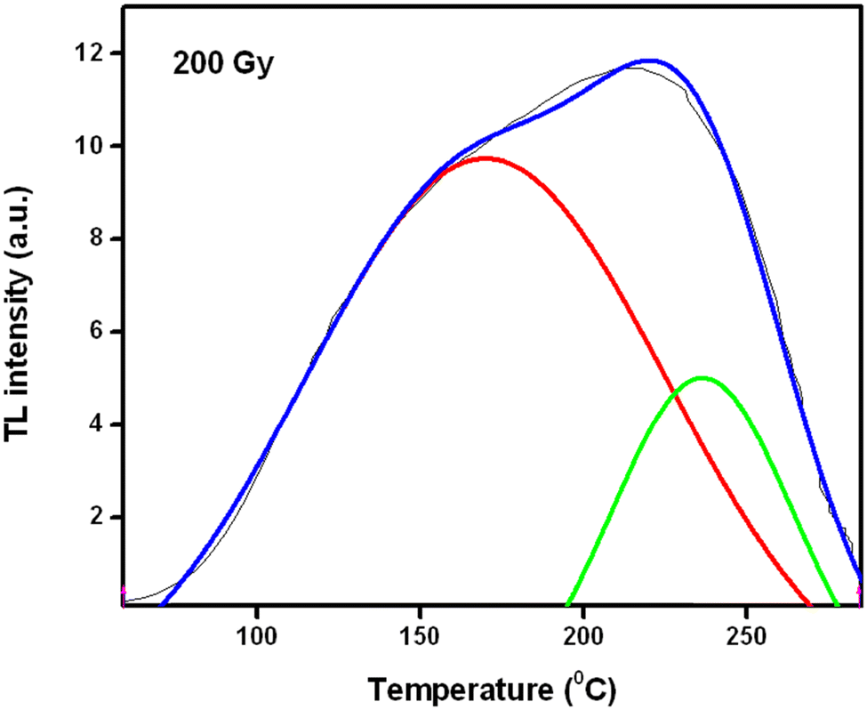 | ||
| Fig. 10 Deconvoluted glow curve of the 2% W doped InO film exposed to a 200 Gy radiation dosage. | ||
Currently, the TLD dosimetry method is utilized in personnel dosimeter and environmental monitoring to measure the exposed radiation doses. The efficiency of the material to trap charge carriers determines its applicability in TL dosimetry. Hence the observed thermoluminescence property of the synthesized material confirms its relevance in dosimetry applications.
3.7. XPS
The chemical states of constituent elements and surface composition of 2 at% W doped thin film was analysed by X-ray photoelectron spectroscopy (XPS). The characteristic line corresponding to adventitious C observed at 284.8 eV in the XPS spectra was considered as a reference for calibrating the binding energies. As samples are conductive, charge compensation is not required. Any residual charging was corrected by post-processing, where spectra were adjusted to align with the reference peak at 284.8 eV and the correction obtained was 0.3 eV. The binding energies of photoelectron lines corresponding to In, O and W determine the chemical status of these elements in the compound.Fig. 11 shows the wide scan spectra of the IWO thin film within a binding energy range of 0–1100 eV and also the core spectrum of In, O and W. The peaks found at 443.98 and 451.53 eV corresponding to In3d5/2 and In3d3/2 spin–orbit levels establish the 3+ state of In in InO. The chemical shift of the In3d5/2 line relative to the In0 (reference data for the average binding energy of 443.5 eV) is 0.9 eV and this shift can be attributed to the In3+ state (based on reference, the expected change in the binding energy of the oxidation of In in InO is +0.8 to 1.2 eV).46
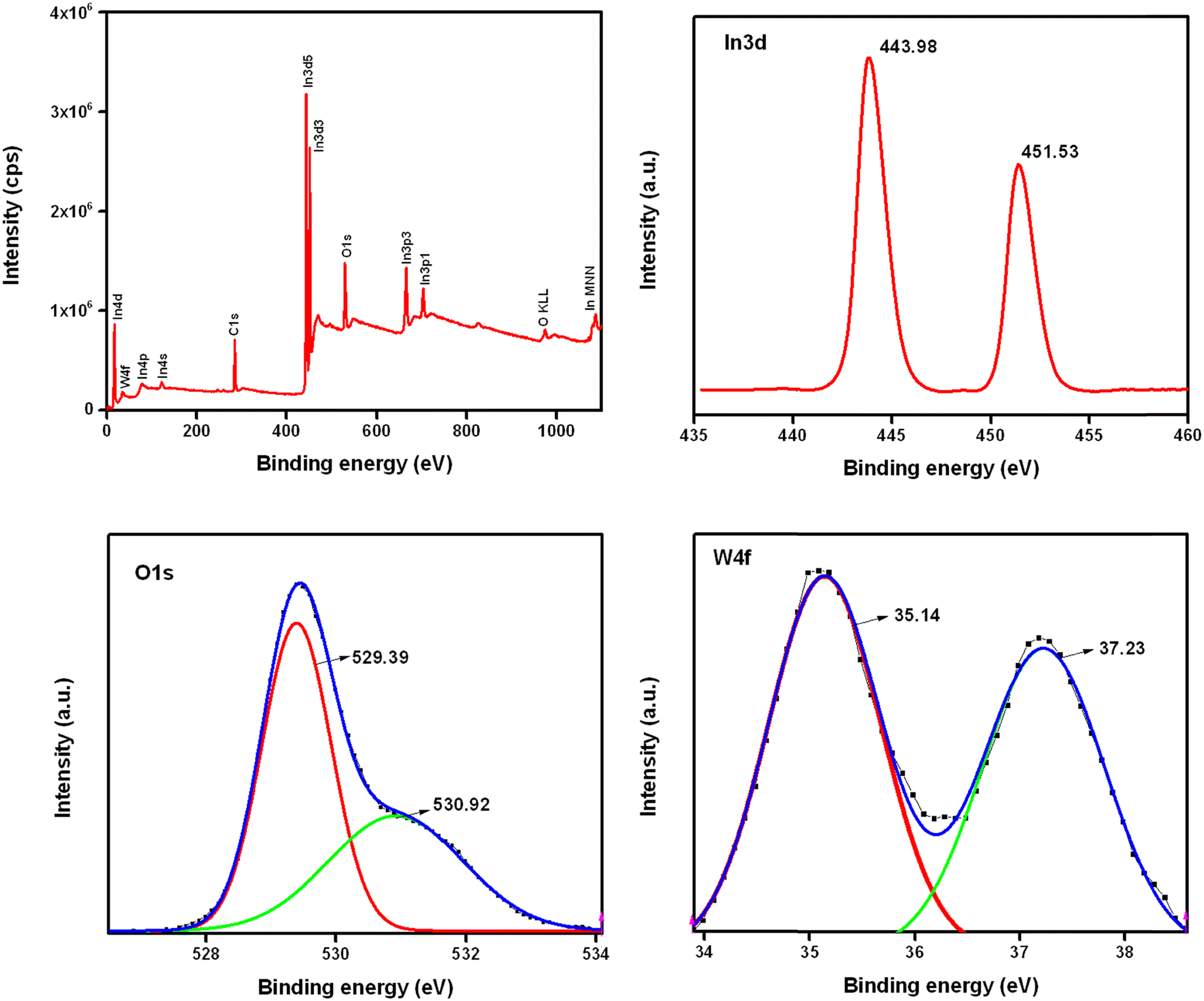 | ||
| Fig. 11 XPS survey spectra and core spectra of In, O and W in W-doped InO thin films. | ||
The doublet observed in the W core spectrum with binding energies 35.14 and 37.23 eV corresponds to W 4f7/2 and W 4f5/2 levels. The observed binding energies confirm the 6+ oxidation state of W. Even though there is a possibility of the formation of other oxidation states like +4, the absence of shoulder peaks or any asymmetry points out the complete oxidization of W dopants to the W6+ state in the film.1
As found in our previous study on pure and Zn-doped indium oxide thin films, here also we found a doublet structure in the O1s core spectrum.13,19 Generally, the oxygen doublet found in metal oxides indicates the formation of mixed valence states.47 The major peak at 529.39 eV suggests the oxygen in the crystal lattice of InO, whereas the 530.92 eV peak can be attributed to non-stoichiometric oxygen.32 However, unlike Zn-doped InO film, W-doped film doesn’t show any trace of unreacted In metal.28 Moreover, the peak positions of O and In are close to that of pristine InO, unlike Zn-doped InO.
3.8. Electrical properties
The Hall effect measurement set up with Van der Pauw configuration is utilized to study the electrical properties of tungsten-doped films at room temperature. Table 5 lists the estimated electrical resistivity, mobility and charge carrier concentration corresponding to each dopant concentration. It is shown in the table that the electrical resistivity of the InO thin film decreased after tungsten doping and the 6 at% doped film shows the least value of resistivity. The comparatively higher resistivity of the 4 at% sample is attributed to the reduced carrier concentration at that doping concentration. The observed high resistivity of 4 at% doped films is due to increased grain boundary scattering.12 Generally, the resistivity is determined by the free carriers found in the conduction band. Hence it can be confirmed that the decreased resistivity of the W-doped InO films can be attributed to increased film carrier concentration. Previous reports support the fact that oxygen vacancies as well as defects can generate carrier electrons and thereby decrease resistivity.22 The decreased resistivity of 2% can be due to the better crystallinity of the sample and less oxygen vacancies.20 According to T. C. Paul et al., the decrease in resistivity can be due to reduced disorder in the lattice after doping or due to higher free electrons or lower hole concentration in the conduction band and valence band.33| Sample | Preferred orientation | Resistivity (Ω cm) | Mobility, μ (cm2 V−1 s−1) | Carrier concentration, n × 1018 (cm−3) |
|---|---|---|---|---|
| IWO_0 | (400) | 0.12 | 28.35 | 1.7719 |
| IWO_2 | (400) | 0.045 | 13.59 | 10.24 |
| IWO_4 | (400) | 0.119 | 13.30 | 3.96 |
| IWO_6 | (400) | 0.031 | 21.19 | 9.51 |
| IWO_8 | (400) | 0.033 | 21.37 | 8.92 |
| IWO_10 | (222) | 0.043 | 21.09 | 7.39 |
Higher carrier concentration was observed in the 2 at% doped thin film whereas 4 at% shows the least. A higher density of W6+ ions in In3+ substitutional sites can be a possible reason for the increased carrier concentration of 2 at% doped films.20 Here in doped films in addition to the oxygen vacancies, the doped ions also provide free carriers as the valencies of the doped ions and host matrix are different.10
The carrier mobility is generally dependent upon different scattering mechanisms like lattice, ionized impurity, neutral impurity, and grain boundary. The neutral impurity scattering and lattice vibration scattering usually found in heavily degenerated films can be neglected. Hence the mobility is controlled by ionized impurities as well as grain boundaries. The decrease in mobility after doping can be attributed to the increased ionized impurity scattering centres. This can deteriorate the conductivity of the films.10 Moreover, as the ionic radii of W6+ ions are lesser than In, the probability for the dopant ions to occupy interstitial positions is higher. This can deform the crystal structure and these inactive dopants at interstitial positions can act as scattering centres, which in turn can reduce the mobility.6
Even though the carrier mobility of the film decreased after doping, it showed a slight increase at higher doping levels. The lower mobility values at lower doping concentrations could be due to higher oxygen content in the film. It is reported that excess O ions act as electron scattering centres, which supports the mobility drop at 2 at%.20 Moreover, decreased grain size can result in an increased grain boundary, related barriers, and surface states, which results in carrier traps. The mobility of the carrier possesses a direct correlation with these carrier traps and hence the decrease in mobility after doping can be due to increased trap centres.12 The increased mobility beyond 4% can be due to the increase in oxygen vacancies.3 It is also noteworthy that the mobility of the IWO thin film is higher than that of the IZO film and for both films, the mobility values are lesser than that of the pristine one. The charge mobility, surface density and dopant distribution, which depend on the crystallographic orientation, can enhance the sensitivity of the material.
The carrier concentration enhanced after W doping, whereas mobility diminished after doping. Hence it can be confirmed that resistivity, Hall mobility and carrier concentration are sensitive to the doping concentration. All three electrical parameters extracted from Hall measurements are sensitive to oxygen vacancies.
4. Conclusion
Tungsten-doped InO thin films were synthesized on the glass substrate using the spray pyrolysis technique with a dopant concentration varying from 2 to 10 at%. A polycrystalline cubic structure with a shift in prominent growth orientation from (400) to (222) at higher doping levels was observed for the deposited film. Cubic crystallization of doped InO with no impurity phase and oxygen vacancy formation is confirmed by Raman spectra. XPS analysis confirms the 6+ oxidation state of tungsten. The decrement in transmittance with an increase in doping concentration can be attributed to the crystal defects that emerged after doping. The redshift in the absorption edge indicates the decrease in bandgap energy. Band tailing increased after doping due to the defect formation. Violet-blue emission was observed in the photoluminescence spectra along with NBE emission. The TL glow curve confirms the applicability of the W-doped InO thin film for dosimetry applications. W doping also influenced the electrical properties of the material. The resistivity decreased with tungsten doping and it is due to the increase in donor electrons. It was observed that the 2 at% W doped InO showed preferred structural, optical and electrical properties with fewer defects. As the 2 at% W doped sample shows the least defects, it is expected to show comparatively higher sensitivity for radiation. InO doped with 2 at% W would be a suitable material for gamma sensing applications.Data Availability
Authors confirm that the data supporting the findings of this study are available within the article.Conflicts of interest
The authors declare that they have no known competing financial interests or personal relationships that could have appeared to influence the work reported in this paper.Acknowledgements
This research did not receive any specific grant from funding agencies in the public, commercial, or not-for-profit sectors. The authors are grateful to CIF MAHE Manipal, India; CRF, NITK, Surathkal, India; DST PURSE Laboratory and CARRT, Mangalore University, Mangalagangothri, India; CIF, IIT, Jammu for extending characterization facilities. Ms Aparna also acknowledges the support received from the Department of Physics, Manipal Academy of Higher Education (MAHE) for providing the scholarship for research work and instrumentation facilities.References
- S. Kumar Vishwanath, T. An, W. Y. Jin, J. W. Kang and J. Kim, The optoelectronic properties of tungsten-doped indium oxide thin films prepared by polymer-assisted solution processing for use in organic solar cells, J. Mater. Chem. C, 2017, 5(39), 10295–10301, 10.1039/c7tc03662k.
- A. Yahia, A. Attafa, H. Saidia, M. Dahnouna, C. Khelifia, A. Bouhdjera, A. Saadia and H. Ezzaouia, Structural, optical, morphological and electrical properties of indium oxide thin films prepared by sol gel spin coating process, Surf. Interfaces, 2019, 14, 158–165, DOI:10.1016/j.surfin.2018.12.012.
- M. Girtan and G. Folcher, Structural and optical properties of indium oxide thin films prepared by an ultrasonic spray CVD process, Surf. Coat. Technol., 2003, 172(2–3), 242–250, DOI:10.1016/S0257-8972(03)00334-7.
- K. Arshak and O. Korostynska, Preliminary studies of properties of oxide thin/thick films for gamma radiation dosimetry, Mater. Sci. Eng., B, 2004, 107(2), 224–232, DOI:10.1016/j.mseb.2003.11.014.
- A. Shokohmanesh and F. Jamali-Sheini, Synthesis and transient photocurrent behavior of Zn-doped In2O3 nanorods, Sens. Actuators, A, 2017, 265, 246–252, DOI:10.1016/j.sna.2017.08.010.
- S. Parthiban, V. Gokulakrishnan, K. Ramamurthi, E. Elangovan, R. Martins, E. Fortunato and R. Ganesan, High near-infrared transparent molybdenum-doped indium oxide thin films for nanocrystalline silicon solar cell applications, Sol. Energy Mater. Sol. Cells, 2009, 93(1), 92–97, DOI:10.1016/j.solmat.2008.08.007.
- T. L. Barr and Y. L. Liu, An x-ray photoelectron spectroscopy study of the valence band structure of indium oxides, J. Phys. Chem. Solids, 1989, 50(7), 657–664, DOI:10.1016/0022-3697(89)90001-2.
- Y. Yamada, N. Suzuki, T. Makino and T. Yoshida, Stoichiometric indium oxide thin films prepared by pulsed laser deposition in pure inert background gas, J. Vac. Sci. Technol., A, 2000, 18(1), 83–86, DOI:10.1116/1.582122.
- P. Prathap, Y. P. V. Subbaiah, M. Devika and K. T. R. Reddy, Optical properties of In2O3 films prepared by spray pyrolysis, Mater. Chem. Phys., 2006, 100, 375–379, DOI:10.1016/j.matchemphys.2006.01.016.
- X. Li, Q. Zhang, W. Miao, L. Huang and Z. Zhang, Transparent conductive oxide thin films of tungsten-doped indium oxide, Thin Solid Films, 2006, 515(4), 2471–2474, DOI:10.1016/j.tsf.2006.07.014.
- C. Aparna, P. K. Shetty, M. G. Mahesha, N. Karunakara and I. Yashodhara, Sensors and Actuators: A. Physical Structural, optical and sensitivity study of optimized indium oxide thin film for gamma sensing applications, Sens. Actuators, A, 2022, 345, 113785, DOI:10.1016/j.sna.2022.113785.
- M. A. Sayeed and H. K. Rouf, Effect of Zn-doping on the structural, optical and electrical properties of thermally vacuum evaporated CdTe thin films, Surf. Interfaces, 2021, 23, 100968, DOI:10.1016/j.surfin.2021.100968.
- C. Aparna, P. K. Shetty and M. G. Mahesha, Investigation on structural, optical and electrical properties of Zn doped indium oxide thin film for gamma dosimetry, Mater. Chem. Phys., 2023, 302, 127712, DOI:10.1016/j.matchemphys.2023.127712.
- C. Agashe, M. G. Takwale, V. G. Bhide, S. Mahamuni and S. K. Kulkarni, Effect of Sn incorporation on the growth mechanism of sprayed SnO2 films, J. Appl. Phys., 1991, 70(12), 7382–7386, DOI:10.1063/1.349733.
- N. Beji, M. Souli, S. Azzaza, S. Alleg and N. K. Turki, Study on the zinc doping and annealing effects of sprayed In2O3 thin films, J. Mater. Sci.: Mater. Electron., 2016, 27(5), 4849–4860, DOI:10.1007/s10854-016-4367-y.
- R. Karmakar, S. K. Neogi, A. Banerjee and S. Bandyopadhyay, Structural; Morphological; optical and magnetic properties of Mn doped ferromagnetic ZnO thin film, Appl. Surf. Sci., 2012, 263, 671–677, DOI:10.1016/j.apsusc.2012.09.133.
- I. Saadeddin, H. S. Hilal, R. Decourt, G. Campet and B. Pecquenard, Indium oxide co-doped with tin and zinc: A simple route to highly conducting high density targets for TCO thin-film fabrication, Solid State Sci., 2012, 14(7), 914–919, DOI:10.1016/j.solidstatesciences.2012.04.021.
- A. G. Imer, Investigation of Al doping concentration effect on the structural and optical properties of the nanostructured CdO thin film, Superlattices Microstruct., 2016, 92, 278–284, DOI:10.1016/j.spmi.2016.01.035.
- C. Aparna, P. K. Shetty and M. G. Mahesha, Materials Science in Semiconductor Processing Structural optimization of indium oxide thin film for gamma dosimetry applications, Mater. Sci. Semicond. Process., 2022, 150, 106931, DOI:10.1016/j.mssp.2022.106931.
- K. Dey, A. G. Aberle, S. van Eek and S. Venkataraj, Superior optoelectrical properties of magnetron sputter-deposited cerium-doped indium oxide thin films for solar cell applications, Ceram. Int., 2021, 47(2), 1798–1806, DOI:10.1016/j.ceramint.2020.09.006.
- K. Usharani and A. R. Balu, Structural, optical, and electrical properties of Zn-doped CdO thin films fabricated by a simplified spray pyrolysis technique, Acta Metall. Sin., 2015, 28(1), 64–71, DOI:10.1007/s40195-014-0168-6.
- R. R. Krishnan, R. S. Sreedharan, S. K. Sudheer, C. Sudarsanakumar, V. Ganesan, P. Srinivasan and V. P. M. Pillai, Effect of tantalum doping on the structural and optical properties of RF magnetron sputtered indium oxide thin films, Mater. Sci. Semicond. Process., 2015, 37, 112–122, DOI:10.1016/j.mssp.2015.02.033.
- M. Souli, M. Reghima, M. Secu, C. Bartha, M. Enculescu, A. Mejri, N. Kamoun-Turki and P. Badica, Physical properties investigation of samarium doped calcium sulfate thin films under high gamma irradiations for space photovoltaic and dosimetric applications, Superlattices Microstruct., 2019, 126, 103–119, DOI:10.1016/j.spmi.2018.12.021.
- K. G. Gopchandran, B. Joseph, J. T. Abraham, P. Koshy and K. V. Vaidyan, The preparation of transparent electrically conducting indium oxide films by reactive vacuum evaporation, Vacuum, 1997, 48(6), 547–550, DOI:10.1016/s0042-207x(97)00023-7.
- G. G. Khan, S. Ghosh, A. Sarkar, G. Mandal, G. D. Mukherjee, U. Manju, N. Banu and B. N. Dev, Defect engineered d 0 ferromagnetism in tin-doped indium oxide nanostructures and nanocrystalline thin-films, J. Appl. Phys., 2015, 118(7), 8, DOI:10.1063/1.4928952.
- C. M. Ghimbeu, M. Lumbreras, M. Siadat and J. Schoonman, Detection of pollutant gases using electrostatic sprayed indium oxide and tin-doped indium oxide, Mater. Chem. Phys., 2009, 114(2–3), 933–938, DOI:10.1016/j.matchemphys.2008.10.072.
- A. Singhal, S. N. Achary, J. Manjanna, O. D. Jayakumar, R. M. Kadam and A. K. Tyagi, Colloidal fe-doped indium oxide nanoparticles: Facile synthesis, structural, and magnetic properties, J. Phys. Chem. C, 2009, 113(9), 3600–3606, DOI:10.1021/jp8097846.
- F. Saeed, A. Farooq, A. Ali, S. Mehmood, C. Cepek, S. Bhardwaj, A. Ul-Hamid and A. S. Bhattia, Anomalous optical behavior in pyramid-like indium oxide (In2O3) nanostructures, Mater. Sci. Eng., B, 2020, 262, 114781, DOI:10.1016/j.mseb.2020.114781.
- H. Lee, B. Kim, C. Y. Gao, H. J. Choi, J. Ko, C. H. Seo and J. Park, “Raman spectroscopy study of solution-processed In2O3 thin films: effect of annealing temperature on the characteristics of In2O3 semiconductors and thin-film transistors, Mol. Cryst. Liq. Cryst., 2019, 679(1), 38–47, DOI:10.1080/15421406.2019.1597544.
- A. Khan, F. Rahman, A. Ahad and P. A. Alvi, Investigation of transport phenomenon and magnetic behavior of Fe doped In2O3, Phys. B, 2020, 592 DOI:10.1016/j.physb.2020.412282.
- T. K. Maity and S. L. Sharma, Effect of gamma radiation on optical and electrical properties of tellurium dioxide thin films, Bull. Mater. Sci., 2008, 31(6), 841–846, DOI:10.1007/s12034-008-0134-x.
- M. A. M. Khan, R. Siwach, S. Kumar, J. Ahmed and M. Ahamed, Hydrothermal preparation of Zn-doped In2O3 nanostructure and its microstructural, optical, magnetic, photocatalytic and dielectric behaviour, J. Alloys Compd., 2020, 846, 156479, DOI:10.1016/j.jallcom.2020.156479.
- T. C. Paul and J. Podder, Synthesis and characterization of Zn-incorporated TiO2 thin films: impact of crystallite size on X-ray line broadening and bandgap tuning, Appl. Phys. A: Mater. Sci. Process., 2019, 125(12), 1–14, DOI:10.1007/s00339-019-3112-9.
- K. Kesavan, A. Kathalingam, H. S. Kim and A. R. U. Sundari, Effects of fluorine doping on structural, optical and electrical properties of spray deposited CdO thin films, Superlattices Microstruct., 2016, 100, 76–88, DOI:10.1016/j.spmi.2016.09.004.
- T. C. Paul, J. Podder and M. H. Babu, Optical constants and dispersion energy parameters of Zn-doped TiO2 thin films prepared by spray pyrolysis technique, Surf. Interfaces, 2020, 21, 100725, DOI:10.1016/j.surfin.2020.100725.
- M. Jothibas, C. Manoharan, S. Ramalingam, S. Dhanapandian and M. Bououdina, Spectroscopic analysis, structural, microstructural, optical and electrical properties of Zn-doped In2O3 thin films, Spectrochim. Acta, Part A, 2014, 122, 171–178, DOI:10.1016/j.saa.2013.11.008.
- N. Singh, C. Yan and P. S. Lee, Room temperature CO gas sensing using Zn-doped In2O3 single nanowire field effect transistors, Sens. Actuators, B, 2010, 150(1), 19–24, DOI:10.1016/j.snb.2010.07.051.
- A. Montazeri and F. Jamali-Sheini, Enhanced ethanol gas-sensing performance of Pb-doped In2O3 nanostructures prepared by sonochemical method, Sens. Actuators, B, 2017, 242, 778–791, DOI:10.1016/j.snb.2016.09.181.
- K. Anand, J. Kaur, R. C. Singh and R. Thangaraj, Preparation and characterization of Ag-doped In2O3 nanoparticles gas sensor, Chem. Phys. Lett., 2017, 682(3), 140–146, DOI:10.1016/j.cplett.2017.06.008.
- K. Sarkar, S. Mukherjee, S. Farid, A. Nicholls, M. A. Stroscio and M. Dutta, Characterization of Co-existing In2O3–ZnO Nanostructures, J. Electron. Mater., 2017, 46(10), 5848–5854, DOI:10.1007/s11664-017-5594-6.
- J. A. Nieto, Thermoluminescence of metallic oxides. Development and applications in Mexico: An overview, Appl. Radiat. Isot., 2018, 138, 35–39, DOI:10.1016/j.apradiso.2017.07.044.
- J. Azorin, Preparation methods of thermoluminescent materials for dosimetric applications: An overview, Appl. Radiat. Isot., 2014, 83, 187–191, DOI:10.1016/j.apradiso.2013.04.031.
- J. I. Lee, D. Lee, J. L. Kim and S. Y. Chang, Thermoluminescence emission spectra for the LiF:Mg,Cu,Na,Si thermoluminescent materials with various concentrations of the dopants (3-D measurement), Radiat. Prot. Dosim., 2006, 119(1–4), 293–299, DOI:10.1093/rpd/nci602.
- R. K. Choudhary, A. Soni, P. Mishra, D. R. Mishra and M. S. Kulkarni, Synthesis of aluminum nitride thin films and their potential applications in solid state thermoluminescence dosimeters, J. Lumin., 2014, 155, 32–38, DOI:10.1016/j.jlumin.2014.06.016.
- Y. S. Horowitz, Theory of thermoluminescence gamma dose response: The unified interaction model, Nucl. Instrum. Methods Phys. Res., Sect. B, 2001, 184(1–2), 68–84, DOI:10.1016/S0168-583X(01)00712-1.
- V. Luhin, I. Zharsky and P. Zhukowski, Application of DC magnetron sputtering for creation of gas-sensitive indium oxide thin films and their properties, Acta Phys. Pol., A, 2013, 123(5), 837–839, DOI:10.12693/APhysPolA.123.837.
- D. Beena, K. J. Lethy, R. Vinodkumar, A. P. Detty, V. P. Mahadevan Pillai and V. Ganesan, Photoluminescence in laser ablated nanostructured indium oxide thin films, J. Alloys Compd., 2010, 489(1), 215–223, DOI:10.1016/j.jallcom.2009.09.055.
| This journal is © The Royal Society of Chemistry 2025 |