
 Open Access Article
 This Open Access Article is licensed under a Creative Commons Attribution-Non Commercial 3.0 Unported Licence
Effect of silver and cobalt on transparent conducting CdO thin films: tuning the optoelectronic properties†
Ishraque
Karim
 a,
M. Ashikul Haque
Naeem
*b,
Ahmed Sidrat Rahman
Ayon
b,
Md. Abdus
Sattar
c,
Md. Abdus
Sabur
*d and
Aninda Nafis
Ahmed
d
a,
M. Ashikul Haque
Naeem
*b,
Ahmed Sidrat Rahman
Ayon
b,
Md. Abdus
Sattar
c,
Md. Abdus
Sabur
*d and
Aninda Nafis
Ahmed
d
aDepartment of Materials Science & Engineering, Rajshahi University of Engineering & Technology (RUET), Rajshahi 6204, Bangladesh
bDepartment of Glass & Ceramic Engineering, Rajshahi University of Engineering & Technology (RUET), Rajshahi 6204, Bangladesh. E-mail: ashiknaeem167@gmail.com
cDepartment of Materials Science & Engineering, University of Rajshahi, Rajshahi 6205, Bangladesh
dPilot Plant and Process Development Centre, Bangladesh Council of Scientific and Industrial Research (BCSIR), Dhanmondi, Dhaka 1205, Bangladesh. E-mail: sabur37971@gmail.com
First published on 6th December 2024
Abstract
Thin film technology is a crucial area of research for the advancement of modern technologies and next-generation applications. In this work, the structural, optoelectrical, and thermal properties of silver (Ag)–cobalt (Co) dual-doped cadmium oxide (CdO) thin films were investigated. Successful incorporation of the doping elements with high crystallinity (maximum value 85%) was confirmed through X-ray diffraction (XRD) analysis, and no unexpected peaks were observed. The pure and doped samples demonstrated a polycrystalline nature with FCC lattice. Scanning electron microscopy (SEM) results revealed the surface microstructures of the deposited 3% Ag–Co doped CdO thin films as spherical or round-shaped agglomerated grains with a smooth surface appearance. From the optical analysis, a maximum transmittance of 89% was observed for the 3% Ag–Co doped CdO sample, which was rarely reported in the literature. Additionally, doping altered the optical band gap from 4.09 eV to 3.88 eV, which enhanced the potential of using the transparent conductive films in optoelectronic devices. Doping CdO with Ag and Co altered its electrical properties, leading to an increase in resistivity and a decrease in carrier concentration. Hall measurements confirmed that all the samples showed an n-type semiconductor behavior. Thermal analysis results demonstrated that the 1% Ag–Co doped CdO sample exhibited the highest thermal conductivity of 2.35 W m−1 K−1, and further increase in the doping concentrations led to a decrease in both the power factor and figure of merit (ZT) values.
1 Introduction
Thin film technology (TF) encompasses a diverse range of materials and methods that have contributed to the advancements of applications across various fields, including electronics, photovoltaics, gas sensing, and energy conversion and storage. Advanced TF technology has become an important area of research in the development of transparent conductive oxides (TCOs), which are essential components in various optoelectronic devices as they have impressive and unique characteristics of high optical transparency and good electrical conductivity.1,2 Among various TCOs, aluminium-doped zinc oxide (AZO),3 indium-doped tin oxide (ITO),4 and fluorine-doped tin oxide (FTO)5 have both good electrical conductivity and optical transparency, making them useful in solar cells,2 flat panel displays,6 and light-emitting diodes (LEDs).7 The ability to control the chemical composition during deposition of the films makes TCOs of binary compounds more promising than the multicomponent oxides,1 such as Cd2SnO4, CdSnO3, and CdIn2O4.8,9CdO is one of the most promising binary TCO materials with widespread applications in optoelectronic and electronic applications owing to its excellent electrical conductivity, good optical transparency throughout the visible spectrum, and impressive carrier density and mobility.10 These remarkable characteristics make CdO a functional choice for diverse applications, such as solar cells, phototransistors, diodes, gas sensors, and antireflection coatings.11 Besides, its optical band gap, ranging from approximately 2.2 eV to 2.5 eV, enables high transmittance in the visible spectrum, making CdO a strong TCO suitable for diverse electronic applications, such as solar cells, and photodiodes.11–13 Lavate et al.14 demonstrated the photodegradation capabilities of CdO thin films, indicating its potential for applications in environmental remediation. This characteristic suggests the applicability of CdO thin films beyond its traditional electronic applications.
Doped CdO thin films have become a pivotal area of research due to their promising properties for various applications, particularly in optoelectronics and gas sensing applications. For instance, doping diverse metallic ions into the CdO lattice can enhance its properties.15 Metal doping can alter the optical properties of materials. The influence of the metal's interaction with electromagnetic waves is based on the free conduction of electrons in the metal. High reflectance may be observed at optical frequencies due to the presence of a negative dielectric constant in many metals.16 Surface plasmon resonance (SPR) is a phenomenon that occurs when P-polarized light hits a metal-coated prism, creating free electrons in the metal surface that can take part in certain interactions, resulting in a collective oscillation known as surface plasmon resonance (SPR).17 The noble metal gold, known for its high oxidation resistance, is mainly used to excite SPR;18 however, given its high cost, other noble materials, such as silver, may also be used to generate SPR.19 Generally, a lower thickness of film generates the maximum SPR effect.20
The electrical properties of thin films cover a wide area due to the different microstructures resulting from different doping materials and concentrations, whether they are metallic films, semiconductors, or insulator films, and the type of substrate on which they are deposited. Doping metallic ions in CdO whose ionic radii are less than that of Cd2+ can improve the electrical conductivity.21 Even with ions with a small radius, the many structural defects and grain boundaries in microstructures can act as obstacles to charge carriers, thereby reducing the conductivity.22 These defects can trap mobile carriers and generate an energy barrier between the crystallites by decreasing the motion of the charge carriers.23
Tin (Sn)-doping of CdO thin films exhibited enhanced conductivity that was 2–5 times higher than that of ITO coatings.24 It was also reported that Y- and In-doping into CdO could alter the transparency and electronic structure of CdO thin films, making them suitable for optoelectronic device applications.25 Neodymium (Nd)-doped CdO exhibited a lower optical band-gap with increasing the Nd concentration, which is important for solar cells and photodetector applications.26 Therefore, the incorporation of suitable dopants into the CdO lattice can significantly influence the structural, optical, and electrical characteristics of CdO films, making them suitable for an extensive range of technological applications. Many studies have reported on doping CdO, including with aluminum (Al),27 silver (Ag),28 copper (Cu),29 zinc (Zn),30 molybdenum (Mo),31 and iron (Fe).32 Many studies have also sought to control the optical and electrical properties of CdO through dual doping with different elements, including Ni–Ga,33 Cu–Fe,34 Zn–Co,35 and Cr–Co.36
Previous studies have emphasized that dual doping can lead to a significant enhancement of the properties of CdO, improving its potential for use in various optoelectronic applications. Mn–Fe dual-doped CdO exhibited improved transmittance due to the Moss–Burstein effect.37 Co-doped CdO thin films with Zn and Ag demonstrated outstanding non-linear optical properties, improved conductivity and, carrier concentrations.38 Tb–Zn dual-doped CdO thin films showed greatly elevated electrical properties with increasing the Tb concentration.39 The incorporation of Zn and Co in CdO thin films promoted the optical transmittance and ferromagnetic properties, which are suitable characteristics for spintronic applications.35 Also, the magnetic properties of CdO thin films were improved by dual doping with Cu and Fe.34 CdO thin films could also attain ferromagnetic properties with Ni–Ga dual doping,33 while Ni–Zn dual doping led to a ferromagnetic transition from paramagnetic, holding promise for a wide range of spintronic applications.40 Among all the potential doping elements, Ag is perhaps the most impressive doping element because of its ability to remove the metal-like behavior of CdO, while increasing the Ag concentration in CdO can enhance both the electrical and optical properties, including reducing the band-gap energy and refractive indices, as reported by Alam et al.41 Zhang et al.42 found that Ag-doping enhanced the near-band edge UV emission in metal oxide films. It was also found that metal doping could increase the conductivity in TCO,43 but excessive metal dopant levels could have a negative impact on the conductivity in TCO because of the introduction of possible defects44 and its lower crystallinity.21 Additionally, the electrical conductivity could also be increased with increasing Ag concentration.45 On the other hand, co-doping helps enhance the optical and electrical properties. It was reported that increasing the cobalt content led to the optical band gap decreasing,46 and the optical transmittance increasing.47 Besides, Co ions can introduce ferromagnetism into the CdO matrix, which would make it suitable for spintronic applications where both the magnetic and electronic functionalities of materials are required.48
However, the consequences of the dual doping of Ag and Co with CdO remain largely unexplored. Motivated by all the prior findings in this field, this research aimed to investigate the dual-doping of Ag and Co with CdO thin films. Demet et al.49 found that the optical transmittance of CdO thin films increased with increasing the Co concentration from 1% to 3%. The optical band-gap and refractive index were found to decrease with increasing the Ag concentration from 1% to 4%.41 Khan et al.50 reported a significant improvement in the optical properties at a higher Ag concentration (4%). Motivated by these findings, we aimed to dope both silver (Ag) and cobalt (Co) in equal percentages ranging from 1% to 4%. Here, all the films were deposited on a glass substrate using spray pyrolysis at 400 °C. We utilized the spray-pyrolysis deposition method for film fabrication, while many previous studies synthesized pure and doped CdO utilizing other methods, including pulse laser deposition,51 spray pyrolysis,52 successive ionic layer adsorption and reaction (SILAR),53 magnetron sputtering,54 sol–gel spin coating,55 and chemical vapor deposition.56 Among these methods, the spray-pyrolysis method is cost-effective and has the unique feature of allowing precise control over the film thickness and doping concentrations. After fabrication of the Ag–Co dual-doped CdO thin films by applying the spray-pyrolysis method, we analyzed the structural, morphological, optical, electrical, and thermal properties of the Ag–Co dual-doped CdO thin films with a view to their application potential. The findings of this research should greatly contribute to the advancement of the general efficiency of optoelectronic devices.
2 Experimental section
2.1 Materials
The materials used for the deposition of the thin films included cadmium acetate dihydrate ([CdCH3(COO)2]·2H2O) as a source for CdO, silver nitrate (AgNO3) for Ag, and cobalt(II) nitrate hexahydrate (Co(NO3)2·6H2O) for Co. These chemicals were sourced from Merck KGaA with purity levels of 99%, 99.8%, and 98%, respectively. The solvent was deionized water, and the substrates used were micro-glass slides.2.2 Deposition of the thin films
Deposition of the CdO thin films on glass substrates was performed using the spray-pyrolysis (SP) method under normal atmospheric conditions, as illustrated in Fig. 1. Both undoped and co-doped CdO thin films were prepared by applying a solution created from separately prepared 0.1 M solutions of each substance dissolved in deionized water. The solutions were mixed using a magnetic stirrer. The compositions of the sprayed solutions are provided in Table 1. A heating plate served as the heat source with a temperature of 400 °C. The chemical solutions were applied on the glass substrates using a nozzle as a spraying apparatus. Prior to the deposition of the thin films, the glass substrates were cleaned with deionized water and organic solvent and then left to dry under normal atmosphere conditions. Next, these glass substrates were slowly heated before placing them on the heating plate, which contributed significantly to minimizing the thermal shock. The distance of the substrate from the atomizer was kept constant at 26 cm. An air compressor operating at 1 bar pressure was employed for each sample, and a liquid flow rate of 1 ml min−1 was utilized. The spray nozzle ensured a uniform deposition of the solution over the substrate, and the time taken for the spraying was 20 min, with a 5-min interval between sprays. The most probable reactions during the thin film deposition process are as given in the following eqn (1) and (2).| [CdCH3(COO)2]·2H2O + H2O Decomposed at 400 °C → CdO + CH4 + CO2 + Steam | (1) |
| [CdCH3(COO)2]·2H2O + AgNO3 + Co (NO3)2·6H2O Decomposed at 400 °C → CdO(Ag:Co) + CH3COOH + NO2 + O2 + Steam | (2) |
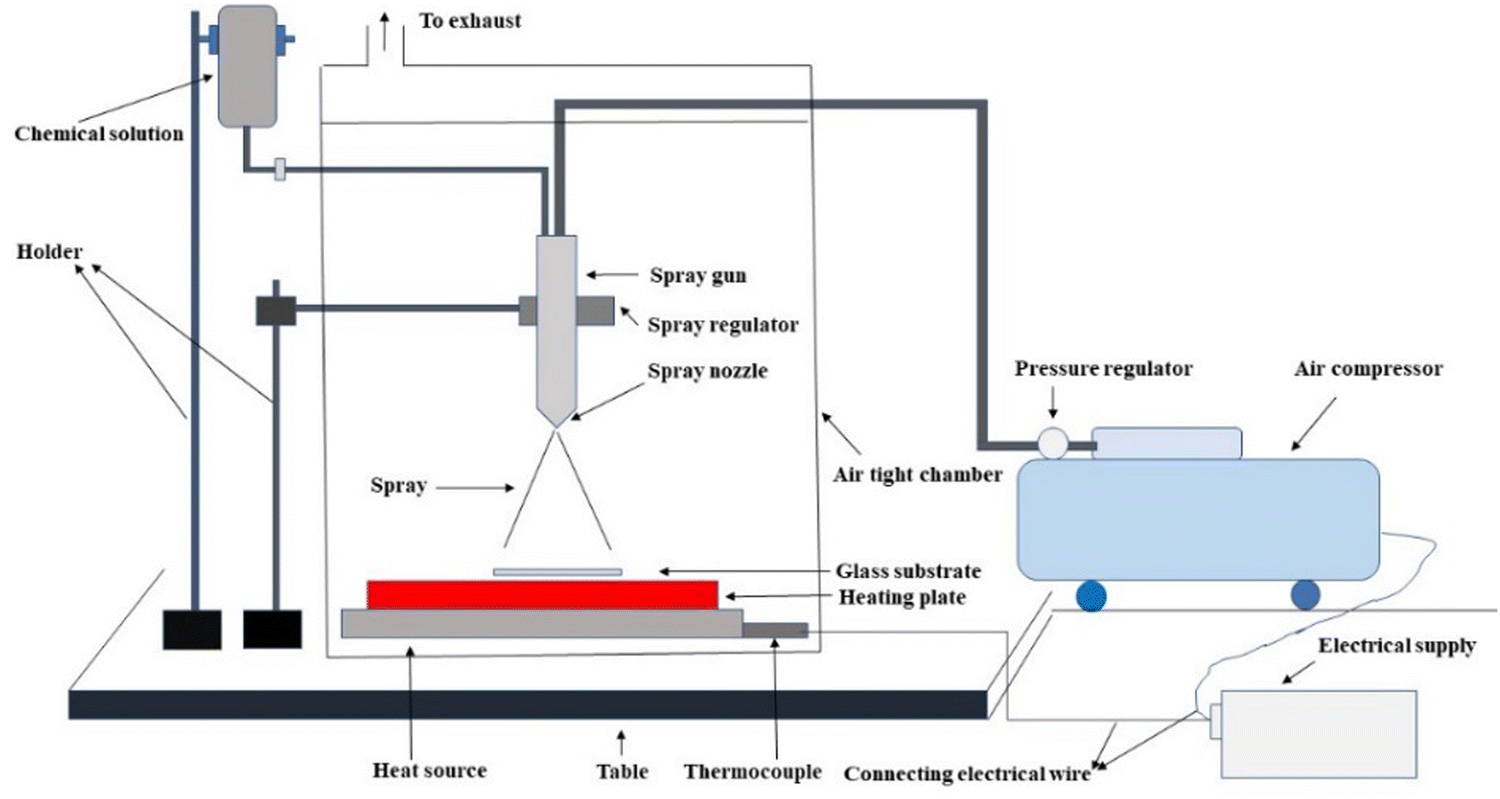 | ||
| Fig. 1 Schematic of the experimental setup. | ||
| Sample | Solution composition |
|---|---|
| CdO | 100% [Cd CH3(COO)2]·2H2O solution |
| CAC-1 | 1% (AgNO3) solution + 1% (Co (NO3)2·6H2O) solution + 98% [CdCH3(COO)2]·2H2O solution |
| CAC-2 | 2% (AgNO3) solution + 2% (Co (NO3)2·6H2O) solution + 96% [CdCH3(COO)2]·2H2O solution |
| CAC-3 | 3% (AgNO3) solution + 3% (Co (NO3)2·6H2O) solution + 94% [CdCH3(COO)2]·2H2O solution |
| CAC-4 | 4% (AgNO3) solution + 4% (Co (NO3)2·6H2O) solution + 92% [CdCH3(COO)2]·2H2O solution |
2.3 Characterization and film analysis
In this study, an X-ray diffractometer (Empyrean EMP 3, Malvern Panalytical) was used to investigate the structural characteristics of the CdO and Ag–Co dual-doped thin films. CuKα (K = 1.5406 Å) X-ray radiation was used to scan every sample between diffraction angles of 20° and 80° at room temperature. The Debye–Scherrer equation (eqn (3)) was utilized to calculate the average sizes of the CdO and CAC crystallites.57 | (3) |
 | (4) |
| V = a3 | (5) |
 | (6) |
 | (7) |
The crystallinity is the proportion of crystalline areas within a material and represents the extent of long-range order in a crystalline substance.61 For measurement of the crystallinity, the total crystalline peak area and the total area (crystalline and amorphous area) were measured using Origin software, and the following equation (eqn (8)) was used to determine the crystallinity.
 | (8) |
The surface morphology of the CdO and Ag–Co dual-doped CdO thin films was characterized by SEM (TESCAN VEGA Compact). Additionally, elemental composition analysis was conducted by energy-dispersive X-ray spectroscopy (EDS) with the same instrument (TESCAN VEGA Compact).
The thickness of the thin film samples was measured using a BRUKER surface profilometer (DktakXT).
A UV-visible spectrophotometer SHIMADZU (Uv-1900i) was used to analyze the optical transmittance (T) and absorbance (A) of the CdO and (Ag–Co) dual-doped CdO thin films within the wavelength range of 350–1100 nm at 25 °C. The optical band gap of the samples was determined using eqn (9), which is commonly known as Tauc's law, where α is a coefficient, A is a constant, h is Plank's constant, ν is the absorption at a specific frequency of light, Eg is the optical band gap, and n is a constant.62
| αhν = A(hν − Eg)n | (9) |
The absorption coefficient values, extinction coefficient (k), and refractive index (nr) were determined using eqn (10)–(12), respectively. In these equations, T represents the transmittance, d is the film thickness,63λ represents the wavelength of light, and r denotes the reflectance.
 | (10) |
 | (11) |
 | (12) |
The Van der Pauw Ecopia HMS-3000 Hall Measurement System was used for electrical analysis. The thin film samples’ conductivity and resistivity were determined using eqn (13), where I is the current, and R is the resistance.64
| V = IR | (13) |
The Hall effect was measured at room temperature using a constant magnetic field of 0.545 T. The determined Hall voltage (VH) was utilized to compute the Hall coefficient (RH), carrier concentration (n), and Hall mobility (μH) using eqn (14)–(16).25,65
 | (14) |
 | (15) |
 | (16) |
A thermal conductivity meter (HOT DISK TPS 500S) was used to determine the thermal conductivity, diffusivity, and specific heat of the undoped and Ag–Co dual-doped CdO samples. The power factor (PF) was calculated from eqn (17), where S is the Seebeck coefficient and ρ is the electrical resistivity.
 | (17) |
The performance of a thermoelectric material is called the figure of merit, which can be determined using the following equation (eqn (18)), where S is the Seebeck coefficient, T is the absolute temperature, ρ is the electrical resistivity, and K is the thermal conductivity.
 | (18) |
3 Result and discussion
3.1 X-ray diffraction (XRD) analysis
The diffraction peaks observed for the (111), (200), (220), (311), and (222) planes confirmed the face-centered cubic (FCC) structure of the CdO, which was consistent with the standard JCPDS card no. 05-0640. These peaks indicated a polycrystalline structure with a face-centered cubic (FCC) lattice. The absence of additional peaks suggested that there were no secondary phases related to the dopants or their oxides, confirming the successful integration of Co and Ag into the CdO lattice. Upon doping with silver, a shift in the preferred orientation from the (200) plane to the (111) plane was observed, with a similar shift reported by Alam et al.41 This shift, along with the slight rightward peak position noted in the XRD patterns, provided further evidence of the successful Co and Ag doping, consistent with Velusamy et al.'s findings.66 The CdO thin film's lattice parameter was found to be very close to the standard value (4.695 Å) as per JCPDS card no. 05-0640 (Fig. 2). | ||
| Fig. 2 (a) X-ray diffraction (XRD) patterns and (b) peak shifting (111) plane of the pure CdO and Ag–Co dual-doped CdO thin films. | ||
The crystallite sizes were calculated using the Debye–Scherrer formula (eqn (3)). The crystallite sizes for the (111) plane ranged from 14.65–43.98 nm (Table 2). The dual-doped samples exhibited larger crystallite sizes compared to the undoped CdO films (Fig. 3). This increase could be attributed to the larger ionic radii and atomic weights of the dopants’ compared to cadmium ions, a phenomenon also observed by Seçkin et al.67 However, the CAC-3 sample exhibited a decrease in crystallite size, likely due to the increased lattice strain and defects caused by incorporating the different-sized dopants, which prevented the crystallites from growing as large as in the CAC-4 sample. The slight increase in crystallite size with Ag-doping was attributed to Ag's substitution of oxygen vacancies at the grain boundaries, which contributed to a reduction in the local strain.41
| Composition | (hkl) | 2θ | FWHM | Crystallite size, D (nm) | d-spacing, (Å) | Lattice parameter, a, (Å) | Unit cell volume | Dislocation density δ × 10−3 (nm−2) | Lattice strain (ε × 10−3) | Crystallinity (%) |
|---|---|---|---|---|---|---|---|---|---|---|
| CdO | (111) | 33.023 | 0.590 | 14.658 | 2.710 | 4.694 | 103.432 | 4.654 | 10.277 | 85.37 |
| CAC-1 | 32.927 | 0.393 | 21.981 | 2.717 | 4.700 | 103.850 | 2.069 | 6.851 | 64.36 | |
| CAC-2 | 33.033 | 0.196 | 43.976 | 2.709 | 4.687 | 102.990 | 0.517 | 3.425 | 69.73 | |
| CAC-3 | 33.029 | 0.590 | 14.658 | 2.709 | 4.687 | 103.023 | 4.653 | 10.277 | 56.60 | |
| CAC-4 | 33.117 | 0.246 | 35.188 | 2.702 | 4.681 | 102.58 | 0.807 | 4.282 | 65.02 | |
| CdO | (200) | 38.274 | 0.639 | 13.731 | 2.349 | 4.699 | 103.769 | 5.303 | 11.124 | 85.37 |
| CAC-1 | 38.315 | 0.196 | 44.815 | 2.347 | 4.695 | 103.531 | 0.497 | 3.408 | 64.36 | |
| CAC-2 | 38.502 | 0.196 | 44.658 | 2.336 | 4.672 | 102.017 | 0.501 | 3.422 | 69.73 | |
| CAC-3 | 38.357 | 0.590 | 14.879 | 2.344 | 4.689 | 103.131 | 4.516 | 10.268 | 56.60 | |
| CAC-4 | 38.391 | 0.393 | 22.321 | 2.342 | 4.685 | 102.871 | 2.006 | 6.845 | 65.02 |
 | ||
| Fig. 3 Variation of the (a) crystallinity and crystallite size and (b) dislocation density and lattice strain of the pure CdO and Ag–Co dual-doped CdO thin films. | ||
The dislocation density (δ), a measure of defects in the crystal structure (eqn (7)), and the lattice strain (ε) (eqn (6)) results indicate that the crystallinity decreased with increasing the doping concentration. This decrease could be attributed to the size differences between Cd and Ag ions, which disrupted the crystalline order, a trend consistent with the observations made by Khan et al.68 The highest crystallinity was observed in the undoped CdO film, while the lowest was in the 3% doped sample CAC-3, likely due to the introduction of significant lattice strain and defects. Upon doping, a reduction in peak intensity was observed, particularly for the (200) and (111) planes, further confirming the successful incorporation of Ag and Co into the CdO lattice, as these dopants introduced strain and disorder into the crystal structure, reducing the overall crystallinity.
3.2 Scanning electron microscopy (SEM) and energy-dispersive spectroscopy (EDS) analyses
SEM is an effective method for analyzing the surface morphology of thin films, and it is widely acknowledged that the surface structure plays a crucial role in device technology applications.69–73 The surface microstructures of the deposited CdO thin films obtained from SEM analysis were compared in Fig. 4. According to the SEM microstructures, all the films had spherical or rounded-shaped agglomerated grains. The pure CdO, CAC-1, and CAC-4 thin films comprised rounded-shaped grains and a few patches where the particles had agglomerated more densely. The CAC-2 and CAC-3 thin films displayed uniformly dispersed, spherical-shaped grains and some tiny agglomerations that were homogeneous. According to the precise analysis with ImageJ software, the CAC-2 thin film contained tiny voids inside its particles, which decreased with increasing the Ag–Co concentration. The average particle size also decreased with increasing the doping concentration, with the CAC-3 thin film showing the lowest average particle size, i.e., 348 nm, leading to its smoother surface appearance compared to in the other SEM images. | ||
| Fig. 4 Scanning electron microscopy images of the pure CdO and Ag–Co dual-doped CdO thin films. | ||
Elemental composition analysis of the pure CdO, CAC-1, CAC-2, CAC-3, and CAC-4 thin films was performed using energy-dispersive spectroscopy (EDS) (Fig. 5). The EDS results confirmed the presence of cadmium, oxygen, silver, and cobalt elements in the produced Ag–Co dual-doped CdO thin films. On the other hand, Cd and O were the only two elements in the pure CdO sample. Ag and Co peaks appeared after doping the CdO thin films with 1%, 2%, 3%, and 4% Ag and Co ions. This indicates that the Ag and Co ions were successfully incorporated into the CdO lattice. As the Ag and Co percentage increased, the atomic percentage of O in the prepared CdO films decreased from 83.94% to 59.92%. The measured atomic and weight percentage ratios of Cd, O, Ag, and Co verified the presence of Ag and Co in the spray-deposited CdO thin films (Table 3).
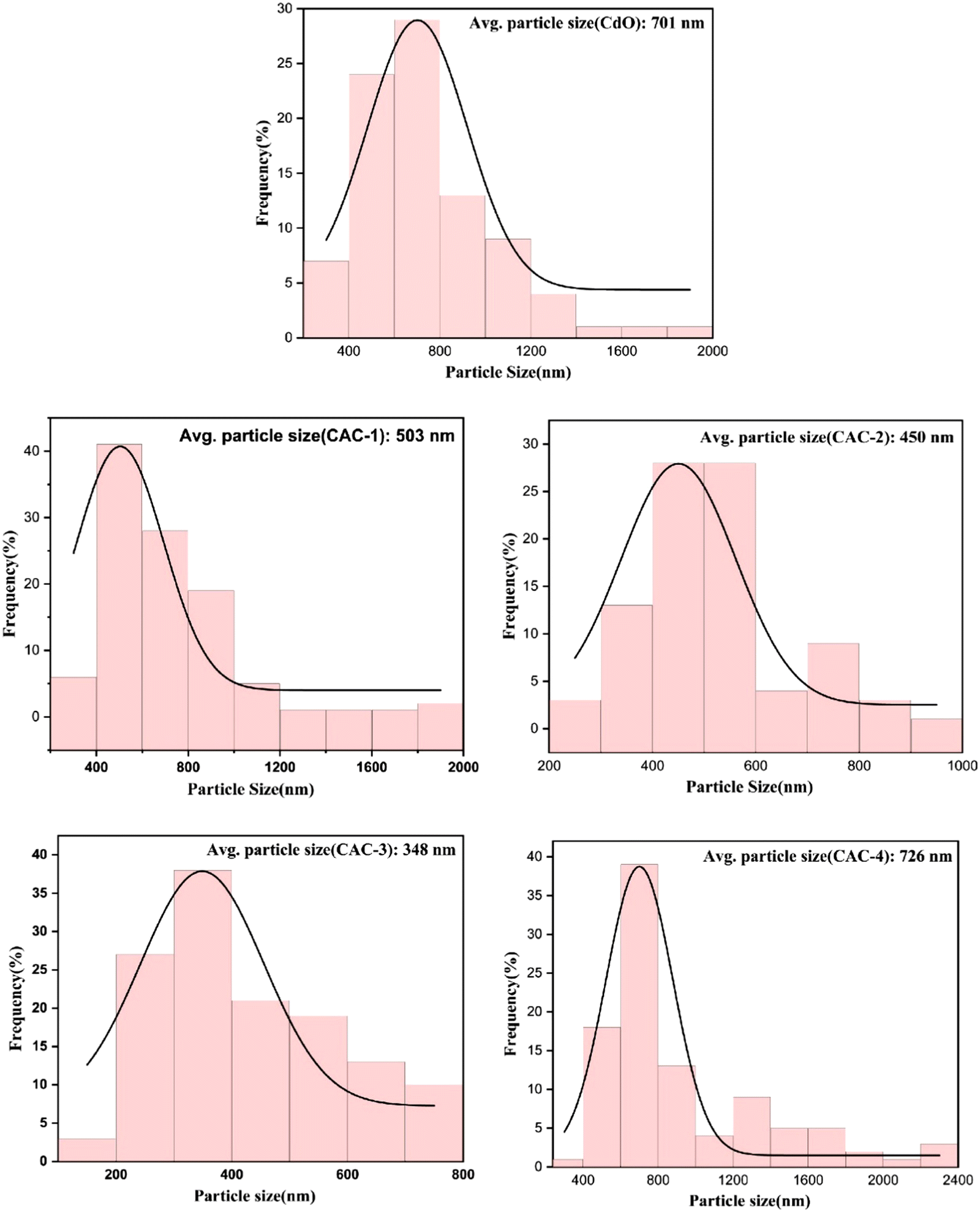 | ||
| Fig. 5 Average particle sizes obtained from the histogram images of pure CdO and Ag–Co dual-doped CdO thin films. | ||
| Sample | Atomic (%) | Weight (%) | ||||||
|---|---|---|---|---|---|---|---|---|
| Cd | O | Ag | Co | Cd | O | Ag | Co | |
| CdO | 16.06 | 83.94 | — | — | 57.34 | 42.66 | — | — |
| CAC-1 | 19.43 | 77.89 | 1.6 | 1.08 | 59.56 | 33.99 | 4.72 | 1.73 |
| CAC-2 | 38.69 | 57.96 | 2.24 | 1.11 | 77.89 | 16.61 | 4.33 | 1.17 |
| CAC-3 | 35.38 | 60.68 | 2.33 | 1.62 | 75.13 | 18.34 | 4.74 | 1.8 |
| CAC-4 | 34.39 | 59.92 | 3.14 | 2.55 | 72.75 | 18.04 | 6.37 | 2.83 |
3.3 Optical analysis
This research observed that the optical behavior of the CdO thin films was influenced by the dual-doping elements Ag and Co introduced into the CdO structure, which improved the material's optical properties.Fig. 6(a) shows the transmittance spectra of the undoped and dual-doped CdO thin films. Except for the CAC-3 sample, the transparency of the dual-doped films was lower than that of the pure CdO thin film. The distortion produced by the dual-doped ions,35 the greater crystallite size,25 and the lower surface roughness74 may be responsible for the decreasing transmittance values. A higher transmittance value of 89% was found in the CAC-3 sample, and the maximum transparency range of 86%–89% stayed in the visible and near-IR region. XRD also showed that the crystallite size of the CAC-3 sample was the lowest (14.65 nm). So, the XRD results strongly support the highest transmittance value of this sample. A sample with a high transmittance value is suitable for functioning in the active region of solar cells.75
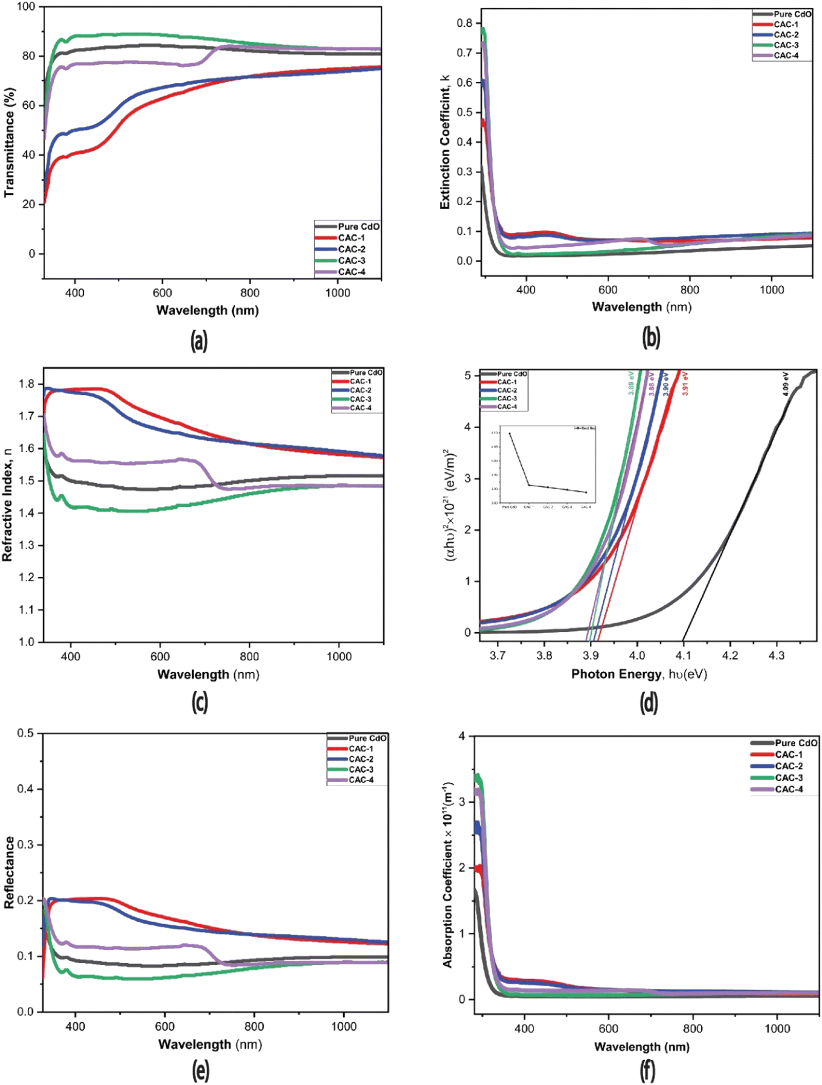 | ||
| Fig. 6 Variations of the (a) optical transmittance, (b) extinction coefficient, (c) refractive index, (d) optical band gap with photon energy, (e) reflectance, and (f) absorption coefficient of the deposited thin films. | ||
The extinction coefficient is related to a material's light-absorbing capacity, and this value was greater for all the dual-doped films than that of the pure CdO thin film (Fig. 6(b)). However, the overall extinction coefficients of all the samples all were less than 0.1. This type of diminished extinction coefficient is suitable for the window layer to transmit light efficiently.75
Fig. 6(c) shows the wavelength-dependent refractive index of the pure and dual-doped CdO thin films. A greater refractive index was found for the lower dual-doped films, and decreased with increasing the doping concentration. Therefore, the dual-doped concentration in the CdO thin film affected the sample's refractive index value. The CAC-3 samples exhibited the lowest refractive index levels. A low surface roughness is a factor in displaying a low refractive index,65.76 From the SEM results, the lowest roughness was noted in the CAC-3 sample, which was the reason for its lowest refractive index. So, this finding was supported by the SEM results.
The direct band gap of the undoped and co-doped CdO thin films was measured by plotting (αhν)2vs. (hν), as shown in Fig. 6(d). A band gap of 4.09 eV was found in the undoped CdO thin film, and a decreased trend was observed with increasing the doping concentration, with bandgaps of 3.91, 3.90, 3.89, and 3.88 eV. Here, we noticed that the double-doped sample maintained a monotonically decreasing series. Although undoped CdO thin films are recognized for having a low band-gap value,77 it can be changed by applying different temperatures, deposition techniques, and thicknesses. Radhika et al. proposed a higher band gap of 3.8 eV for pure CdO thin films, which aligned with our recent research findings.78 The creation of a high dislocation density has the potential to enhance the energy band-gap value also.79 Usharani et al.77 and Azzaoui et al.58 reported band-gap values of 2.46 and 2.41 eV, respectively, for pure CdO thin films, where the dislocation density was noticed on 10−4 (lines per nm2) scales. In our present work, the dislocation density was found on a scale of 10−3 (lines per nm2), which is greater than in previous work and resulted in the higher band-gap value. The reduced band-gap value of cobalt-doped CdO was caused by the greater sp–d interactions of exchange involving the sp band electrons and the localized d electrons of Co2+ ions.80 Dual-doped CdO films,46,81 Fe-doped CdO NPs82 and co-doped ZnO NPs83 were also reported to display a similar behavior. Dakhel et al.84 suggested that the band gap decreases due to the interposition of impurity energy levels into the intrinsic host CdO band gap.
Band-gap broadening or a blue-shift was observed with decreasing the doping concentration, which occurred with a higher carrier concentration,66 as also supported by the XRD results. This can also be explained by the Burstein–Moss effect.85,86 Khalaf et al.87 found a similar band-gap range of 3.95–3.18 eV when cobalt was doped in to a CdO thin film. Nithin et al.47 and Sahin et al.81 also elicited that a lower band-gap value occurs with a higher doping concentration. However, Velusamy et al.66 disclosed that a blue-shift of the band-gap value occurred with increasing the doping concentration.
Moreover, factors like the presence of impurities, the deposition conditions, grain size, thickness, and crystallinity can affect the energy band-gap value.88 Overall, a higher band-gap value is applicable in military, power conversion, and radio applications for allowing adequately handling power of high voltages, temperatures, and frequencies.21
Fig. 6(e) and (f) show the reflectance and absorption coefficient values of the undoped and dual-doped CdO thin films. By increasing the doping concentration, the reflectance value increased, albeit for the CAC-3 sample, a lower reflectance was noticed. Higher roughness is the main factor responsible for higher reflectance.46 The reflectance values were supported by the SEM results, where a lower roughness was found in the CAC-3 sample. Fig. 6(f) shows that the absorption coefficient increased with increasing the doping concentration, but all samples showed a lower absorption coefficient, which was suitable for window-layer applications.89
3.4 Electrical analysis
Fig. 7(a) illustrates that the doped samples had higher resistivity compared to the pure CdO sample, and the CAC-3 sample showed the highest resistivity, i.e., 3.32 × 10⁻² Ω cm.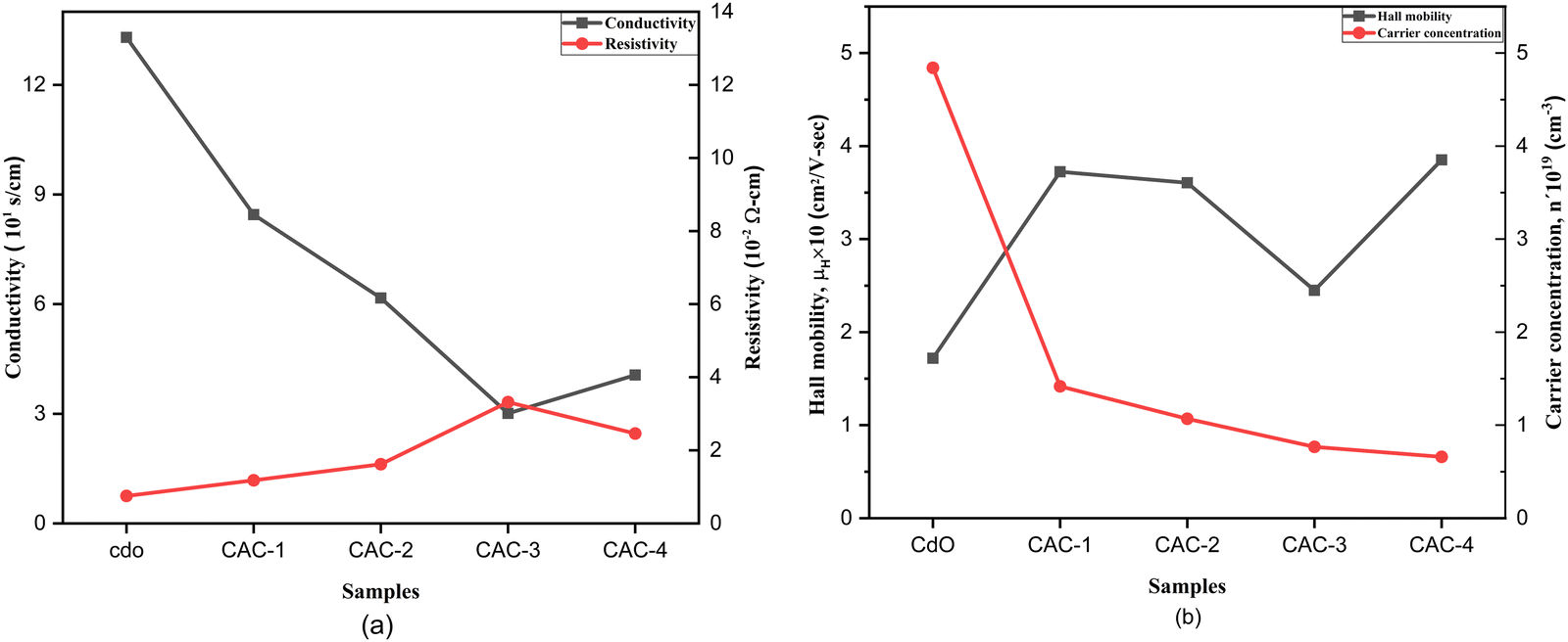 | ||
| Fig. 7 Variations of the (a) resistivity and conductivity, and (b) Hall mobility (μH) and carrier concentrations (n) of the pure CdO and Ag–Co dual-doped CdO thin films. | ||
The ineffectiveness of the dopants in donating free electrons was the factor that increased the resistivity.25,90,91 A lower Hall mobility and carrier concentration were also noticed in the CAC-3 sample, which are other factors for its highest resistivity.
The decrease in resistivity can be attributed to this higher crystallinity.21 According to the XRD analysis, the sample with the lowest conductivity (CAC-3) had the lowest crystallinity too (56%), while the sample with the highest conductivity (pure CdO) had the highest crystallinity (85%). The increase in the quantity of defects within the thin films was caused by a decrease in the crystallinity.21 Compared to pure CdO, this increase in flaws led to greater resistance. Thus, there was a strong correlation between the effect of this on the electrical properties and the XRD results.
Using the Hall effect, other electrical properties such as the Hall mobility (μH), carrier concentration (n), and Hall coefficient (RH) of the undoped and co-doped CdO thin films were also measured at room temperature, and are summarized in Table 4. The negative sign of the Hall coefficient alludes to the fact that the carriers of all the samples were n-type carriers.
| Sample | Resistivity (Ω cm) | Hall mobility, μH (cm2 V−1 s−1) | Carrier concentrations, n (cm−3) | Hall coefficient, RH (cm3 C−1) |
|---|---|---|---|---|
| CdO | 0.75 × 10⁻² | 17.19 | 4.84 × 10¹⁹ | −0.12 |
| CAC-1 | 1.18 × 10⁻² | 37.23 | 1.41 × 10¹⁹ | −0.44 |
| CAC-2 | 1.62 × 10⁻² | 36.05 | 1.06 × 10¹⁹ | −0.58 |
| CAC-3 | 3.32 × 10⁻² | 24.49 | 0.76 × 10¹⁹ | −0.81 |
| CAC-4 | 2.46 × 10⁻² | 38.51 | 0.65 × 10¹⁹ | −0.94 |
The variations of the Hall mobility (μH) and carrier concentration (n) are shown schematically in Fig. 7(b). We noticed that with increasing the doping concentration, the carrier concentration (n) decreased, and the value of all samples was in the order of ∼1019 (cm−3), which matches the reported value for Sr-doped CdO films64 and Y-doped CdO thin films.25 The increase in interstitial impurities was the main factor for the decreasing carrier concentration.25,92 Numerous researchers have examined the Hall mobility of cadmium oxide (CdO) thin films with various metal dopants, such as tin-doped CdO, where the impact of grain boundary scattering has been identified as a significant factor that influences the electron-transport mechanism.93 In the current work, the reduction in grain boundary scattering was the primary factor contributing to the increase in carrier mobility.81 Among the doped samples, CAC-3 exhibited the lowest carrier mobility due to the increase in scattering effect. Additionally, for a lower carrier concentration, the overall lowest conductivity was noticed in the CAC-3 sample. With increasing the doping concentration, the Hall mobility increased, and the highest value was 38.51 cm2 V−1 s−1 found in the CAC-4 sample, which also had the lowest value of carrier concentration. Due to the decreased carrier concentration, the Hall mobility increased.64 However, Drude's theory is well supported by the behavior of the carrier concentration and Hall mobility in both doped and undoped CdO films.94,95 Some electrical and optical data comparisons are given in Table 5 for different types of samples deposited in different methods.
| Method | Doping content | Resistivity (Ω cm) | Carrier concentration (cm−3) | Mobility (cm2 V−1 s−1) | % T | Ref. |
|---|---|---|---|---|---|---|
| Spray pyrolysis | 3% Ag + 3% Co + 94% CdO | 3.32 × 10⁻² | 0.76 × 10¹⁹ | 24.49 | 89 | This work |
| Spray pyrolysis | 100% CdO | 0.75 × 10⁻² | 4.84 × 10¹⁹ | 17.19 | 84 | This work |
| Spray pyrolysis | 3% Sr + 97% CdO | ∼6.2 × 10⁻⁴ | 1.84 × 10¹⁹ | 719 | ∼65 | 64 |
| Spray pyrolysis | 0.25% Co + 99.75% CdO | 7.31 × 10⁻² | 1.11 × 10²⁰ | 80 | ∼83 | 66 |
| DC sputtering | 0.5 wt% Al + 0.5 wt% In | 7.9 × 10⁻⁴ | ∼80 | 96 | ||
| Dual DC sputtering | 0.5 wt% Al2O3 doped ZnO + 5 wt% ZnO doped In2O3 | 2.32 × 10⁻⁴ | ∼1021 | ∼28 | ∼85 | 97 |
| RF sputtering | 1–7 at% Al + 1–7 at% In | ∼2.5 × 10⁻² | 5 × 10¹⁹ | 6.3 | >80 | 98 |
| Chemical spray technique | 1 at% Al + 3 at% In | ∼3.03 × 10⁻² | ∼6 × 10²⁰ | ∼2 | ∼80 | 99 |
| Ultrasonic spray pyrolysis | 1.5 at% Al + 1.5 at% ln | 2.35 × 10⁻³ | 70 | 100 |
3.5 Thermal analysis
Fig. 8 shows the thermal conductivity, thermal diffusivity, and specific heat measured at room temperature. It can be seen that the thermal conductivity and the specific heat increased with increasing the doping percentage from 1% to 4% for the Ag–Co dual-doped elements. | ||
| Fig. 8 Plots of the thermal conductivity, thermal diffusivity, and specific heat of the pure CdO and Ag–Co dual-doped CdO thin films. | ||
The thermal conductivity is the capacity of a material to conduct heat. The thermal conductivity value is the sum of the lattice thermal conductivity and electronic thermal conductivity. Lattice thermal conductivity dominates the total thermal conductivity. Electron–phonon interactions strongly affect the heat-transfer mechanism of films.101 The introduction of possible defects and porosity can lead to an increase in phonon scattering, which can reduce the thermal conductivity.102 Varghese et al.103 highlighted that variations in the defects and porosity could lead to thermal conductivity values in the range of 1–3 W m−1 K−1, and this present work also found the value of thermal conductivity was in the same range. The lowest thermal conductivity value of the pure CdO sample was 1.70 W m−1 K−1. Lower thermal conductivity has also been found in Cd-rich samples, as observed by A. M. M. T. Karim et al.104 In Cd-rich samples, higher electrical resistivity was also noticed. These would be helpful for achieving low thermal conductivity and high electrical performance in thermoelectric devices.105,106 A moderate range of thermal conductivity is useful in electronics as a thermal interface material, where moderate heat conduction is required to manage heat transfer between heat sinks and components. As the doping concentration increased, the value of the specific heat increased, and the highest specific heat of the CAC-3 sample was 0.33 MJ m−3 K−1, suggesting it would be useful in applications requiring moderate heat storage, temperature stability, and energy efficiency.107 Thermal diffusivity is a measurement of the heat conductivity through a material relative to its ability to store thermal energy.108 The highest thermal diffusivity of 9.59 mm2 s−1 was noticed in the CAC-1 sample, but the overall value was lower, and this would be helpful in applications where the material needs to maintain a stable temperature or provide thermal buffering (Fig. 9).
 | ||
| Fig. 9 Power factors and figures of merit (ZT) of the pure CdO and Ag–Co dual-doped CdO thin films. | ||
The power factor (PF) of the pure CdO and Ag–Co dual-doped CdO thin films was calculated from eqn (17). The dimensionless quantity used to determine and evaluate the performance of a thermoelectric material is called the figure of merit, which is given by eqn (18).
The power factor of all the samples decreased with increasing the doping concentration, and the lowest value of 0.11 × 10⁻³ W m−1 K−2 was noticed in the CAC-3 sample. The highest power factor was 0.59 × 10⁻³ W m−1 K−2 for the pure CdO thin film. The figure of merit in a thermoelectric device reflects its effectiveness in converting heat to electricity or thermoelectric performance. By increasing the doping concentration, the ZT value decreased. The highest ZT value noticed in pure CdO was 0.11, and the lowest was in CAC-3, which was 0.01.
According to the formula, materials with a high thermal conductivity, Seebeck coefficient, and low thermal conductivity are considered suitable thermoelectric materials.109,110 The highest ZT value is applicable in thermoelectric devices (Table 6).111
| Sample | System | PF × 10−3 (W m−1 K−2) | ZT | Temperature (K) | Ref. |
|---|---|---|---|---|---|
| ZnO | Thin film | 0.18 | 0.017 | 333 | 112 |
| ZnO | Thin film | 0.11 | 0.009 | 300 | 113 |
| ZnO | Thin film | 0.33 | 0.003 | 300 | 114 |
| ZnO/Si | Thin film | 0.04 | 0.004 | 283 | 115 |
| ZnO/Al | Thin film | 0.08 | 0.11 | 300 | 116 |
| ZnO/Al | Thin film | 0.2 | 0.121 | 320 | 117 |
| ZnO(Ga,In) | Thin film | 0.3 | 0.186 | 573 | 118 |
| ZnO:Al/silica | Thin film | 0.11 | 0.007 | 300 | 119 |
| Sc:ZnCdO | Bulk | 0.71 | 0.30 | 1173 | 120 |
| Cd1−xZnxO | Bulk | 1.1 | 0.52 | 1000 | 121 |
| ZnO–CdO | Thin film | 0.27 | 0.59 | 413 | 122 |
| CdO | Thin film | 0.59 | 0.11 | 303 | This work |
| CdO (Ag 3%, Co 3%) | Thin film | 0.11 | 0.01 | 303 | This work |
4 Conclusion
In this study, pure CdO and Ag–Co dual-doped CdO thin films were deposited on a glass substrate by using the spray-pyrolysis method at 400 °C. The significant structural, morphological, optoelectrical and thermal properties were explored for offering innovative solutions across various fields, including electronics, photovoltaics, and solar cell applications. The slight rightward peak position shift noted in the XRD patterns confirmed the successful Ag and Co doping into the CdO lattice. Scanning electron microscopy analysis illustrated that all the films had spherical-shaped agglomerated grains, and, the 3% Ag–Co doped CdO film exhibited a smooth surface compared to the other films, which indicates it can be used in gas sensors and optoelectronics applications, as a smooth surface would minimize scattering losses. The maximum optical transmittance of 89% from this study can be essential for applications in solar cells, where light absorption is critical for energy conversion. Hall measurements were used to quantify the lowest resistance, which was 1.18 × 10⁻² Ohm cm, among the doped samples, which would be suitable for applications requiring efficient charge transport. Thermal analysis indicated that the thermal conductivity increased with increasing the doping concentration, which could be useful in electronic sensors and thermoelectric applications. This study provides new insights that could be useful for the advancements of optoelectronics applications.Author contributions
Ishraque Karim: writing – review & editing, writing – original draft, funding acquisition, methodology, investigation, formal analysis, data curation, conceptualization. M Ashikul Haque Naeem: writing – review & editing, writing – original draft, methodology, investigation, formal analysis, data curation, conceptualization. Ahmed Sidrat Rahman Ayon: writing – editing. Md. Abdus Sattar: writing – review & editing, supervision, project administration, formal analysis, conceptualization. Md. Abdus Sabur: characterization, review, project administration, supervision. Aninda Nafis Ahmed: resource & supervision.Data availability
Data will be made available on request.Conflicts of interest
The authors declare that they have no known competing financial interests or personal relationships that could have appeared to influence the work reported in this paper.Acknowledgements
This research did not receive any specific grant from funding agencies in the public, commercial, or not-for-profit sectors. The authors would like to acknowledge department of Materials Science & Engineering, University of Rajshahi for lab facility. All the experiments for this research have been performed at Bangladesh Council of Scientific and Industrial Research (BCSIR), Dhaka. Gratitude to Dr Ishtiaque Robin, Postdoctoral Researcher, Pacific Northwest National Laboratory (PNNL), WA, USA, Dr Tanvir Mahmud Bin Hossain, Agriculture Specialist, Foreign Agricultural Service USDA, US Embassy, Dhaka, and Rashida Karim, Teacher, Academia Outstanding English Medium School, Dhanmondi, Dhaka for the encouraging guidelines and continuous support throughout the whole research.References
- T. Minami, Transparent Conductive Oxides for Transparent Electrode Applications, Semicond. Semimetals, 2013, 88, 159–200, DOI:10.1016/B978-0-12-396489-2.00005-9 , Elsevier.
- R. A. Afre, N. Sharma, M. Sharon and M. Sharon, Transparent Conducting Oxide Films for Various Applications: A Review, Rev. Adv. Mater. Sci., 2018, 53(1), 79–89, DOI:10.1515/rams-2018-0006.
- G. B. Murdoch, S. Hinds, E. H. Sargent, S. W. Tsang, L. Mordoukhovski and Z. H. Lu, Aluminum doped zinc oxide for organic photovoltaics, Appl. Phys. Lett., 2009, 94(21), 213301, DOI:10.1063/1.3142423.
- V. Senthilkumar, P. Vickraman, M. Jayachandran and C. Sanjeeviraja, Structural and optical properties of indium tin oxide (ITO) thin films with different compositions prepared by electron beam evaporation, Vacuum, 2010, 84(6), 864–869, DOI:10.1016/j.vacuum.2009.11.017.
- Z. Banyamin, P. Kelly, G. West and J. Boardman, Electrical and Optical Properties of Fluorine Doped Tin Oxide Thin Films Prepared by Magnetron Sputtering, Coatings, 2014, 4(4), 732–746, DOI:10.3390/coatings4040732.
- T. Minami, S. Takata and T. Kakumu, New multicomponent transparent conducting oxide films for transparent electrodes of flat panel displays, J. Vac. Sci. Technol. Vac. Surf. Films, 1996, 14(3), 1689–1693, DOI:10.1116/1.580320.
- H. Liu, V. Avrutin, N. Izyumskaya, Ü. Özgür and H. Morkoç, Transparent conducting oxides for electrode applications in light emitting and absorbing devices, Superlattices Microstruct., 2010, 48(5), 458–484, DOI:10.1016/j.spmi.2010.08.011.
- K. L. Chopra, S. Major and D. K. Pandya, Transparent conductors—A status review, Thin Solid Films, 1983, 102(1), 1–46, DOI:10.1016/0040-6090(83)90256-0.
- X. Wu, W. P. Mulligan and T. J. Coutts, Recent developments in RF sputtered cadmium stannate films, Thin Solid Films, 1996, 286(1–2), 274–276, DOI:10.1016/S0040-6090(95)08527-0.
- B. Sahin and R. Aydin, SILAR derived CdO films: Effect of triethanolamine on the surface morphology and optical bandgap energy, Phys. B, 2018, 541, 95–102, DOI:10.1016/j.physb.2018.04.043.
- R. Ahmad, H. Qays, J. Hussein, G. Hameed and I. Razzaq, Study of physical properties of CdO Thin film prepared by Chemical spray pyrolysis Technique, Diyala J. Pure Sci., 2017, 13(4), 91–105, DOI:10.24237/djps.1304.318E.
- R. H. Bari and S. B. Patil, Nanostructured CdO Thin Films for LPG and CO2 Gas Sensor Prepared by Spray Pyrolisis Technique, Int. Lett. Chem. Phys. Astron., 2014, 37, 31–46, DOI:10.56431/p-lfu9x5.
- B. Hymavathi, B. R. Kumar and T. S. Rao, Studies on optoelectronic properties of DC reactive magnetron sputtered chromium doped CdO thin films, presented at the LIGHT AND ITS INTERACTIONS WITH MATTER, NIT, CALICUT, Kerala, India, 2014, 673(601), 75–79, DOI:10.1063/1.4898222.
- D. Lavate, V. Sawant and A. Khomane, Photodegradation of Rhodamine-B Dye under Natural Sunlight using CdO, Bull. Chem. React. Eng. Catal., 2022, 17(2), 466–475, DOI:10.9767/bcrec.17.2.14172.466-475.
- H. Khamh, E. Sachet, K. Kelly, J.-P. Maria and S. Franzen, As good as gold and better: conducting metal oxide materials for mid-infrared plasmonic applications, J. Mater. Chem. C, 2018, 6(31), 8326–8342, 10.1039/C7TC05760A.
- L. Novotny and B. Hecht, Principles of Nano-Optics, Cambridge University Press, 1st edn, 2006 DOI:10.1017/CBO9780511813535.
- M. Shen and M. G. Somekh, A General Description of the Performance of Surface Plasmon Sensors Using a Transmission Line Resonant Circuit Model, IEEE Sens. J., 2019, 19(23), 11281–11288, DOI:10.1109/JSEN.2019.2933320.
- L. Wu, H. S. Chu, W. S. Koh and E. P. Li, Highly sensitive graphene biosensors based on surface plasmon resonance, Opt. Express, 2010, 18(14), 14395, DOI:10.1364/OE.18.014395.
- K. Shah, N. K. Sharma and V. Sajal, Analysis of fiber optic SPR sensor utilizing platinum based nanocomposites, Opt. Quantum Electron., 2018, 50(6), 265, DOI:10.1007/s11082-018-1533-x.
- D. Michel, F. Xiao and K. Alameh, A compact, flexible fiber-optic Surface Plasmon Resonance sensor with changeable sensor chips, Sens. Actuators, B, 2017, 246, 258–261, DOI:10.1016/j.snb.2017.02.064.
- M. A. Haque Naeem, et al., Insights into the consequence of (Al–Zn) dual-doping on structural, morphological, and optoelectrical properties of CdO thin films, Heliyon, 2024, 10(4), e26545, DOI:10.1016/j.heliyon.2024.e26545.
- E. Acosta, Thin Films/Properties and Applications, in Thin Films, ed. A. Esther Ares, IntechOpen, 2021 DOI:10.5772/intechopen.95527.
- J. Y. W. Seto, The electrical properties of polycrystalline silicon films, J. Appl. Phys., 1975, 46(12), 5247–5254, DOI:10.1063/1.321593.
- S. Ghosh, M. Saha, S. Paul and S. K. De, Shape Controlled Plasmonic Sn Doped CdO Colloidal Nanocrystals: A Synthetic Route to Maximize the Figure of Merit of Transparent Conducting Oxide, Small, 2017, 13(7), 1602469, DOI:10.1002/smll.201602469.
- S. Ahmed, M. S. I. Sarker, M. M. Rahman, M. Kamruzzaman and M. K. R. Khan, Effect of yttrium(Y) on structural, morphological and transport properties of CdO thin films prepared by spray pyrolysis technique, Heliyon, 2018, 4(8), e00740, DOI:10.1016/j.heliyon.2018.e00740.
- M. Ravikumar, et al., Effect of Nd doping on structural and opto-electronic properties of CdO thin films fabricated by a perfume atomizer spray method, Bull. Mater. Sci., 2019, 42(1), 8, DOI:10.1007/s12034-018-1688-x.
- B. Saha, S. Das and K. K. Chattopadhyay, Electrical and optical properties of Al doped cadmium oxide thin films deposited by radio frequency magnetron sputtering, Sol. Energy Mater. Sol. Cells, 2007, 91(18), 1692–1697, DOI:10.1016/j.solmat.2007.05.025.
- M. Yüksel, B. Şahin and F. Bayansal, Nano structured CdO films grown by the SILAR method: Influence of silver-doping on the morphological, structural and optical properties, Ceram. Int., 2016, 42(5), 6010–6014, DOI:10.1016/j.ceramint.2015.12.154.
- M. Benhaliliba, et al., Luminescence and physical properties of copper doped CdO derived nanostructures, J. Lumin., 2012, 132(10), 2653–2658, DOI:10.1016/j.jlumin.2012.03.044.
- V. K. Gupta, A. Fakhri, S. Tahami and S. Agarwal, Zn doped CdO nanoparticles: Structural, morphological, optical, photocatalytic and anti-bacterial properties, J. Colloid Interface Sci., 2017, 504, 164–170, DOI:10.1016/j.jcis.2017.05.026.
- S. J. Helen, S. Devadason, M. Haris and T. Mahalingam, Transparent Conducting Mo-Doped CdO Thin Films by Spray Pyrolysis Method for Solar Cell Applications, J. Electron. Mater., 2018, 47(4), 2439–2446, DOI:10.1007/s11664-018-6079-y.
- M. S. Shalaby, N. M. Yousif, H. Gamal and M. O. Alziyadi, Fe dopant controlled the ferromagnetic, structural, thermal, optical, and electrical characteristics of CdO nanoparticles, Results Chem., 2024, 7, 101260, DOI:10.1016/j.rechem.2023.101260.
- A. A. Dakhel, Generation of Magnetic Properties in Degenerated Ni and Ga Codoped CdO Nanocrystals, J. Supercond. Novel Magn., 2020, 33(6), 1871–1877, DOI:10.1007/s10948-020-05446-w.
- A. A. Dakhel, M. El-Hilo and M. Bououdina, Ferromagnetic properties of Cu- and Fe-codoped nanocrystalline CdO powders: Annealing in hydrogen promote long-range ferromagnetic order, Adv. Powder Technol., 2014, 25(6), 1839–1844, DOI:10.1016/j.apt.2014.07.015.
- T. Noorunnisha, et al., (Zn + Co) co-doped CdO thin films with improved figure of merit values and ferromagnetic orderings with low squareness ratio well suited for optoelectronic devices and soft magnetic materials applications, Appl. Phys. A: Mater. Sci. Process., 2020, 126(10), 762, DOI:10.1007/s00339-020-03954-z.
- T. Munawar, et al., Facile synthesis of Cr-Co co-doped CdO nanowires for photocatalytic, antimicrobial, and supercapacitor applications, J. Alloys Compd., 2021, 885, 160885, DOI:10.1016/j.jallcom.2021.160885.
- N. Manjula, et al., Optoelectronic, magnetic and antibacterial properties of CdO thin films doubly doped with Mn (cationic) and F (anionic) ions, J. Mater. Sci.: Mater. Electron., 2017, 28(11), 7615–7621, DOI:10.1007/s10854-017-6454-0.
- Z. R. Khan, A. S. Alshammari, Mohd S. Khan, M. Mohamed, M. Gandouzi and Mohd Shkir, Tailoring of structural, opto-nonlinear and electrical properties of CdO thin films via Zn and Ag co-doping for optoelectronics applications, Micro Nanostructures, 2022, 168, 207292, DOI:10.1016/j.micrna.2022.207292.
- R. Sarath Babu, Y. Narasimha Murthy, K. Hari Prasad, V. Ganesh and S. AlFaify, Improved optoelectronic properties of Terbium co-doped CdO:Zn thin films coated by nebulizer spray pyrolysis method, Superlattices Microstruct., 2020, 147, 106685, DOI:10.1016/j.spmi.2020.106685.
- T. Noorunnisha, M. Suganya, V. S. Nagarethinam and A. R. Balu, Improved Haacke's quality factor and paramagnetic-to-ferromagnetic transition realized in Ni co-doped CdO:Zn thin films, J. Mater. Sci.: Mater. Electron., 2020, 31(15), 12169–12177, DOI:10.1007/s10854-020-03763-3.
- M. R. Alam, M. Mozibur Rahman, A. M. M. Tanveer Karim and M. K. R. Khan, Effect of Ag incorporation on structural and opto-electric properties of pyrolized CdO thin films, Int. Nano Lett., 2018, 8(4), 287–295, DOI:10.1007/s40089-018-0251-5.
- Y. Zhang, Z. Zhang, B. Lin, Z. Fu and J. Xu, Effects of Ag Doping on the Photoluminescence of ZnO Films Grown on Si Substrates, J. Phys. Chem. B, 2005, 109(41), 19200–19203, DOI:10.1021/jp0538058.
- S. Singh, V. Sharma and K. Sachdev, Investigation of effect of doping concentration in Nb-doped TiO2 thin films for TCO applications, J. Mater. Sci., 2017, 52(19), 11580–11591, DOI:10.1007/s10853-017-1328-7.
- I. B. Miled, et al., Structural, optical, and electrical properties of cadmium oxide thin films prepared by sol–gel spin-coating method, J. Sol-Gel Sci. Technol., 2017, 83(2), 259–267, DOI:10.1007/s10971-017-4412-1.
- K. Mohanraj, D. Balasubramanian, J. Chandrasekaran and A. C. Bose, Synthesis and characterizations of Ag-doped CdO nanoparticles for P–N junction diode application, Mater. Sci. Semicond. Process., 2018, 79, 74–91, DOI:10.1016/j.mssp.2018.02.006.
- A. M. El Sayed and A. Ibrahim, Structural and optical characterizations of spin coated cobalt-doped cadmium oxide nanostructured thin films, Mater. Sci. Semicond. Process., 2014, 26, 320–328, DOI:10.1016/j.mssp.2014.05.019.
- K. V. Kannan Nithin and M. Rm, Krishnappa, Synthesis and characterization of cobalt-doped cadmium oxide thin films prepared by sol–gel spin coating method, J. Phys.: Conf. Ser., 2019, 1362(1), 012118, DOI:10.1088/1742-6596/1362/1/012118.
- A. A. Dakhel and W. E. Alnaser, Physicochemical, structural and induced ferromagnetic properties of Co–In-codoped CdO synthesised via Cd chloride: significant effect of post-treatment hydrogen, Bull. Mater. Sci., 2016, 39(7), 1843–1850, DOI:10.1007/s12034-016-1327-3.
- D. İskenderoğlu, H. Güney, M. E. Güldüren and M. Albayrak, A comprehensive study on SILAR grown cobalt doped CdO thin films, Optik, 2022, 254, 168658, DOI:10.1016/j.ijleo.2022.168658.
- Z. R. Khan, et al., Effect of Ag doping on structural, morphological and optical properties of CdO nanostructured thin films, Phys. B, 2022, 632, 413762, DOI:10.1016/j.physb.2022.413762.
- M. Yan, M. Lane, C. R. Kannewurf and R. P. H. Chang, Highly conductive epitaxial CdO thin films prepared by pulsed laser deposition, Appl. Phys. Lett., 2001, 78(16), 2342–2344, DOI:10.1063/1.1365410.
- O. Vigil, F. Cruz, A. Morales-Acevedo, G. Contreras-Puente, L. Vaillant and G. Santana, Structural and optical properties of annealed CdO thin films prepared by spray pyrolysis, Mater. Chem. Phys., 2001, 68(1–3), 249–252, DOI:10.1016/S0254-0584(00)00358-8.
- M. M. Beevia, M. Anusuyab and V. Saravananc, Characterization of CdO Thin Films Prepared By SILAR Deposition Technique, Int. J. Chem. Eng. Appl., 2010, 151–154, DOI:10.7763/IJCEA.2010.V1.26.
- P. Sakthivel, R. Murugan, S. Asaithambi, M. Karuppaiah, S. Rajendran and G. Ravi, Radio frequency magnetron sputtered CdO thin films for optoelectronic applications, J. Phys. Chem. Solids, 2019, 126, 1–10, DOI:10.1016/j.jpcs.2018.10.031.
- F. Dagdelen, Z. Serbetci, R. K. Gupta and F. Yakuphanoglu, Preparation of nanostructured Bi-doped CdO thin films by sol–gel spin coating method, Mater. Lett., 2012, 80, 127–130, DOI:10.1016/j.matlet.2012.04.087.
- X. Li, et al., Properties of CdO Thin Films Produced by Chemical Vapor Deposition, Electrochem. Solid-State Lett., 2001, 4(6), C43, DOI:10.1149/1.1369216.
- A. O. Bokuniaeva and A. S. Vorokh, Estimation of particle size using the Debye equation and the Scherrer formula for polyphasic TiO 2 powder, J. Phys.: Conf. Ser., 2019, 1410(1), 012057, DOI:10.1088/1742-6596/1410/1/012057.
- W. Azzaoui, et al., Rietveld refinement combined with first-principles study of Zn and Al–Zn doped CdO thin films and their structural, optical and electrical characterisations, J. Mater. Sci.: Mater. Electron., 2023, 34(12), 1010, DOI:10.1007/s10854-023-10384-z.
- N. Manjula and A. R. Balu, Double doping (Mn + Cl) effects on the structural, morphological, photoluminescence, optoelectronic properties and antibacterial activity of CdO thin films, Optik, 2017, 130, 464–472, DOI:10.1016/j.ijleo.2016.10.074.
- I. K. Robin, D. J. Sprouster, N. Sridharan, L. L. Snead and S. J. Zinkle, Synchrotron based investigation of anisotropy and microstructure of wire arc additive manufactured Grade 91 steel, J. Mater. Res. Technol., 2024, 29, 5010–5021, DOI:10.1016/j.jmrt.2024.02.230.
- İ. Uzun, Methods of determining the degree of crystallinity of polymers with X-ray diffraction: a review, J. Polym. Res., 2023, 30(10), 394, DOI:10.1007/s10965-023-03744-0.
- M. Banuprakash, et al., Structural, linear and nonlinear optical characterization of Ni and Al Co-Doped CdO semiconductor nanostructures for nonlinear optical device applications, Mater. Today Proc., 2021, 35, 396–404, DOI:10.1016/j.matpr.2020.02.766.
- R. Kumaravel, K. Ramamurthi and V. Krishnakumar, Effect of indium doping in CdO thin films prepared by spray pyrolysis technique, J. Phys. Chem. Solids, 2010, 71(11), 1545–1549, DOI:10.1016/j.jpcs.2010.07.021.
- M. H. Kabir, A. Bhattacharjee, M. M. Islam, M. S. Rahman, Md. S. Rahman and M. K. R. Khan, Effect of Sr doping on structural, morphological, optical and electrical properties of spray pyrolized CdO thin films, J. Mater. Sci.: Mater. Electron., 2021, 32(3), 3834–3842, DOI:10.1007/s10854-020-05127-3.
- M. Azizar Rahman and M. K. R. Khan, Effect of annealing temperature on structural, electrical and optical properties of spray pyrolytic nanocrystalline CdO thin films, Mater. Sci. Semicond. Process., 2014, 24, 26–33, DOI:10.1016/j.mssp.2014.03.002.
- P. Velusamy, R. R. Babu, K. Ramamurthi, E. Elangovan, J. Viegas and M. Sridharan, Gas sensing and opto-electronic properties of spray deposited cobalt doped CdO thin films, Sens. Actuators, B, 2018, 255, 871–883, DOI:10.1016/j.snb.2017.08.147.
- S. Akın, G. Karanfil, A. Gültekin and S. Sönmezoğlu, Improvement of physical properties of CdO thin films by Au–Ag nanocluster codoping, J. Alloys Compd., 2013, 579, 272–278, DOI:10.1016/j.jallcom.2013.06.059.
- Z. R. Khan, et al., Effect of Ag doping on structural, morphological and optical properties of CdO nanostructured thin films, Phys. B, 2022, 632, 413762, DOI:10.1016/j.physb.2022.413762.
- M. Yüksel, B. Şahin and F. Bayansal, Nano structured CdO films grown by the SILAR method: Influence of silver-doping on the morphological, structural and optical properties, Ceram. Int., 2016, 42(5), 6010–6014, DOI:10.1016/j.ceramint.2015.12.154.
- M. Anitha, K. Saravanakumar, N. Anitha and L. Amalraj, Influence of fluorine doped CdO thin films by an simplified spray pyrolysis technique using nebulizer, Opt. Quantum Electron., 2019, 51(6), 187, DOI:10.1007/s11082-019-1901-1.
- I. K. Robin, et al., Evaluation of Tungsten—Steel Solid-State Bonding: Options and the Role of CALPHAD to Screen Diffusion Bonding Interlayers, Metals, 2023, 13(8), 1438, DOI:10.3390/met13081438.
- T. Gräning, L. Tan, I. Robin, Y. Katoh and Y. Yang, A novel design of transitional layer structure between reduced activation ferritic martensitic steels and tungsten for plasma facing materials, J. Mater. Res. Technol., 2023, 24, 4285–4299, DOI:10.1016/j.jmrt.2023.04.019.
- I. K. Robin, T. Gräning, Y. Yang, Y. Katoh and S. J. Zinkle, Microstructure and thermal stability of a structurally graded tungsten and reduced activation ferritic/martensitic steel joint, J. Mater. Res. Technol., 2024, 30, 3663–3674, DOI:10.1016/j.jmrt.2024.04.087.
- M. Ashaduzzman, M. K. R. Khan, A. M. M. Tanveer Karim and M. Mozibur Rahman, Influence of chromium on structural, non-linear optical constants and transport properties of CdO thin films, Surf. Interfaces, 2018, 12, 135–144, DOI:10.1016/j.surfin.2018.05.008.
- D. M. A. Latif, I. H. Shallal and A. A. Shuihab, Synthesis and study of some physical properties of cadmium oxide CdO thin films, Energy Procedia, 2019, 157, 611–618, DOI:10.1016/j.egypro.2018.11.226.
- M. H. Kabir, M. M. Ali, M. A. Kaiyum and M. S. Rahman, Effect of annealing temperature on structural morphological and optical properties of spray pyrolized Al-doped ZnO thin films, J. Phys. Commun., 2019, 3(10), 105007, DOI:10.1088/2399-6528/ab496f.
- K. Usharani and A. R. Balu, Structural, Optical, and Electrical Properties of Zn-Doped CdO Thin Films Fabricated by a Simplified Spray Pyrolysis Technique, Acta Metall. Sin. (Engl. Lett.), 2015, 28(1), 64–71, DOI:10.1007/s40195-014-0168-6.
- V. Radhika, V. Annamalai, G. Vijaya and D. Annakkodi, Optical and structural properties of doped and undoped CdO thin films, J. Environ. Nanotechnol., 2016, 5(3), 39–43, DOI:10.13074/jent.2016.09.163203.
- A. K. Madkour, F. Rogti, L. Aissani, A. Hamdi, A. Belgroune and A. Zoukel, Effect of annealing treatment on oxalic acid-assisted electrodeposited CdS thin films for enhanced solar cell performance, J. Mater. Sci.: Mater. Electron., 2024, 35(30), 1967, DOI:10.1007/s10854-024-13751-6.
- M. Bouloudenine, N. Viart, S. Colis, J. Kortus and A. Dinia, Antiferromagnetism in bulk Zn1−xCoxO magnetic semiconductors prepared by the coprecipitation technique, Appl. Phys. Lett., 2005, 87(5), 052501, DOI:10.1063/1.2001739.
- B. Sahin, F. Bayansal, M. Yüksel and H. A. Çetinkara, Influence of annealing to the properties of un-doped and Co-doped CdO films, Mater. Sci. Semicond. Process., 2014, 18, 135–140, DOI:10.1016/j.mssp.2013.11.014.
- R. Ranjithkumar, A. Albert Irudayaraj, G. Jayakumar, A. Dhayal Raj, S. Karthick and R. Vinayagamoorthy, Synthesis and Properties of CdO and Fe doped CdO Nanoparticles, Mater. Today Proc., 2016, 3(6), 1378–1382, DOI:10.1016/j.matpr.2016.04.018.
- M. Naeem, S. K. Hasanain and A. Mumtaz, Electrical transport and optical studies of ferromagnetic cobalt doped ZnO nanoparticles exhibiting a metal–insulator transition, J. Phys.: Condens. Matter, 2008, 20(2), 025210, DOI:10.1088/0953-8984/20/02/025210.
- A. A. Dakhel, Structural and optoelectronic properties of Zn-incorporated CdO films prepared by sol–gel method, J. Alloys Compd., 2012, 539, 26–31, DOI:10.1016/j.jallcom.2012.05.117.
- P. V. Kamat, N. M. Dimitrijevic and A. J. Nozik, Dynamic Burstein-Moss shift in semiconductor colloids, J. Phys. Chem., 1989, 93(8), 2873–2875, DOI:10.1021/j100345a003.
- B. Hymavathi, B. R. Kumar and T. S. Rao, Structural, Surface Morphological and Optical Properties of Cr Doped CdO Thin Films for Optoelectronic Devices, Mater. Today Proc., 2015, 2(4–5), 1510–1517, DOI:10.1016/j.matpr.2015.07.077.
- A. Khalaf, M. Matar and W. Abdeen, Tunable Band Gap and Antiferromagnetic Ordering in Co-doped CdO Nanostructures, J. Supercond. Novel Magn., 2021, 34(11), 2911–2921, DOI:10.1007/s10948-021-05973-0.
- W. Z. Tawfik, Z. S. Khalifa, M. Sh Abdel-wahab and A. H. Hammad, Sputtered cobalt doped CuO nano-structured thin films for photoconductive sensors, J. Mater. Sci.: Mater. Electron., 2019, 30(2), 1275–1281, DOI:10.1007/s10854-018-0395-0.
- M. K. R. Khan, et al., Effect of Al-doping on optical and electrical properties of spray pyrolytic nano-crystalline CdO thin films, Curr. Appl. Phys., 2010, 10(3), 790–796, DOI:10.1016/j.cap.2009.09.016.
- R. Nallendran, G. Selvan and A. R. Balu, Photocatalytic Performance of SnO2 Coupled CdO Nanoparticles Against MY and RhB Dyes, J. Electron. Mater., 2019, 48(6), 3676–3685, DOI:10.1007/s11664-019-07125-6.
- K. Sankarasubramanian, et al., Influence of Mn doping on structural, optical and electrical properties of CdO thin films prepared by cost effective spray pyrolysis method, Mater. Sci. Semicond. Process., 2014, 26, 346–353, DOI:10.1016/j.mssp.2014.05.005.
- R. K. Gupta, K. Ghosh, R. Patel, S. R. Mishra and P. K. Kahol, Highly conducting and transparent tin-doped CdO thin films for optoelectronic applications, Mater. Lett., 2008, 62(25), 4103–4105, DOI:10.1016/j.matlet.2008.06.008.
- M. Vigneshwar, R. Chandiramo, B. G. Jeyaprakas and D. Balamuruga, Physical Properties of Spray Deposited Mg Doped CdO Thin Films, J. Appl. Sci., 2012, 12(16), 1754–1757, DOI:10.3923/jas.2012.1754.1757.
- A. M. M. T. Karim, M. K. R. Khan and M. M. Rahman, Structural and opto-electrical properties of pyrolized ZnO—CdO crystalline thin films, J. Semicond., 2015, 36(5), 053001, DOI:10.1088/1674-4926/36/5/053001.
- S. H. Brewer and S. Franzen, Calculation of the electronic and optical properties of indium tin oxide by density functional theory, Chem. Phys., 2004, 300(1–3), 285–293, DOI:10.1016/j.chemphys.2003.11.039.
- T. Tohsophon, N. Wattanasupinyo, B. Silskulsuk and N. Sirikulrat, Effect of aluminum and indium co-doping on zinc oxide films prepared by dc magnetron sputtering, Thin Solid Films, 2011, 520(2), 726–729, DOI:10.1016/j.tsf.2011.06.079.
- J.-H. Bae and H.-K. Kim, Characteristics of Al doped ZnO co-sputtered InZnO anode films prepared by direct current magnetron sputtering for organic light-emitting diodes, Thin Solid Films, 2008, 516(21), 7866–7870, DOI:10.1016/j.tsf.2008.05.035.
- S. D. Kirby and R. B. Van Dover, Improved conductivity of ZnO through codoping with In and Al, Thin Solid Films, 2009, 517(6), 1958–1960, DOI:10.1016/j.tsf.2008.10.066.
- A. Hadri, M. Taibi, A. E. Hat and A. Mzerd, Transparent and conductive Al/F and In co-doped ZnO thin films deposited by spray pyrolysis, J. Phys.: Conf. Ser., 2016, 689, 012024, DOI:10.1088/1742-6596/689/1/012024.
- V. K. Jayaraman, A. Maldonado-Álvarez, A. E. Jimenez-Gonzalez and M. D. L. L. Olvera-Amador, Influence of precursor ball milling in enhancing the structural, morphological, optical and electrical properties of AIZO thin films, Mater. Lett., 2016, 181, 52–55, DOI:10.1016/j.matlet.2016.06.007.
- Md. R. Islam, et al., Evaluating size effects on the thermal conductivity and electron–phonon scattering rates of copper thin films for experimental validation of Matthiessen's rule, Nat. Commun., 2024, 15(1), 9167, DOI:10.1038/s41467-024-53441-9.
- S. Cao, H. He and W. Zhu, Defect induced phonon scattering for tuning the lattice thermal conductivity of SiO2 thin films, AIP Adv., 2017, 7(1), 015038, DOI:10.1063/1.4975227.
- R. Varghese, H. Harikrishna, S. T. Huxtable, W. T. Reynolds and S. Priya, Effect of Crystallinity on Thermal Transport in Textured Lead Zirconate Titanate Thin Films, ACS Appl. Mater. Interfaces, 2014, 6(9), 6748–6756, DOI:10.1021/am500482r.
- A. M. Md and T. Karim, et al., Ultrahigh Thermoelectric Performance of ZnO–CdO Thin Films, J. Electron. Mater., 2024, 53(1), 188–195, DOI:10.1007/s11664-023-10761-8.
- J.-H. Lee, et al., Enhancing the thermoelectric properties of super-lattice Al2O3/ZnO atomic film via interface confinement, Ceram. Int., 2016, 42(13), 14411–14415, DOI:10.1016/j.ceramint.2016.06.032.
- K. Mahmood, et al., Investigation of the optimal annealing temperature for the enhanced thermoelectric properties of MOCVD-grown ZnO films, J. Exp. Theor. Phys., 2017, 124(4), 580–583, DOI:10.1134/S1063776117040045.
- S. M. Hasnain, Review on sustainable thermal energy storage technologies, Part I: heat storage materials and techniques, Energy Convers. Manag., 1998, 39(11), 1127–1138, DOI:10.1016/S0196-8904(98)00025-9.
- A. Bouguerra, A. Aït-Mokhtar, O. Amiri and M. B. Diop, Measurement of thermal conductivity, thermal diffusivity and heat capacity of highly porous building materials using transient plane source technique, Int. Commun. Heat Mass Transf., 2001, 28(8), 1065–1078, DOI:10.1016/S0735-1933(01)00310-4.
- J.-H. Lee, et al., Enhancing the thermoelectric properties of super-lattice Al2O3/ZnO atomic film via interface confinement, Ceram. Int., 2016, 42(13), 14411–14415, DOI:10.1016/j.ceramint.2016.06.032.
- K. Mahmood, et al., Investigation of the optimal annealing temperature for the enhanced thermoelectric properties of MOCVD-grown ZnO films, J. Exp. Theor. Phys., 2017, 124(4), 580–583, DOI:10.1134/S1063776117040045.
- X. Zhang, H. Li and J. Wang, Effect of sintering temperature on thermoelectric properties of CdO ceramics, J. Adv. Ceram., 2015, 4(3), 226–231, DOI:10.1007/s40145-015-0153-1.
- K. Kim, et al., Anomalous thermoelectricity of pure ZnO from 3D continuous ultrathin nanoshell structures, Nanoscale, 2018, 10(6), 3046–3052, 10.1039/C7NR08167G.
- G. Li, S. Liu, Y. Piao, B. Jia, Y. Yuan and Q. Wang, Joint improvement of conductivity and Seebeck coefficient in the ZnO:Al thermoelectric films by tuning the diffusion of Au layer, Mater. Des., 2018, 154, 41–50, DOI:10.1016/j.matdes.2018.05.019.
- A. I. Abutaha, S. R. Sarath Kumar and H. N. Alshareef, Crystal orientation dependent thermoelectric properties of highly oriented aluminum-doped zinc oxide thin films, Appl. Phys. Lett., 2013, 102(5), 053507, DOI:10.1063/1.4790644.
- N. H. Tran Nguyen, et al., Thermoelectric Properties of Indium and Gallium Dually Doped ZnO Thin Films, ACS Appl. Mater. Interfaces, 2016, 8(49), 33916–33923, DOI:10.1021/acsami.6b10591.
- V. Sethi, et al., Ultralow Thermal Conductivity and Improved Thermoelectric Properties of Al-Doped ZnO by In Situ O2 Plasma Treatment, Small Struct., 2023, 4(11), 2300140, DOI:10.1002/sstr.202300140.
- S. Liu, G. Li, M. Lan, M. Zhu, K. Miyazaki and Q. Wang, Role of intrinsic defects on thermoelectric properties of ZnO:Al films, Ceram. Int., 2021, 47(12), 17760–17767, DOI:10.1016/j.ceramint.2021.03.098.
- A. T. T. Pham, et al., Effect of annealing temperature on thermoelectric properties of Ga and In dually doped – ZnO thin films, J. Alloys Compd., 2018, 747, 156–165, DOI:10.1016/j.jallcom.2018.02.349.
- S. Saini, et al., Effect of self-grown seed layer on thermoelectric properties of ZnO thin films, Thin Solid Films, 2016, 605, 289–294, DOI:10.1016/j.tsf.2015.09.060.
- L. Han, et al., Scandium-doped zinc cadmium oxide as a new stable n-type oxide thermoelectric material, J. Mater. Chem. A, 2016, 4(31), 12221–12231, 10.1039/C6TA03126A.
- X. Zha, et al., Towards a high thermoelectric performance in CdO ceramics by introducing multiscale scattering centers via ZnCO3 doping, Mater. Res. Express, 2018, 5(3), 035908, DOI:10.1088/2053-1591/aab5ee.
- A. M. Md and T. Karim, et al., Ultrahigh Thermoelectric Performance of ZnO–CdO Thin Films, J. Electron. Mater., 2024, 53(1), 188–195, DOI:10.1007/s11664-023-10761-8.
Footnote |
| † Electronic supplementary information (ESI) available. See DOI: https://doi.org/10.1039/d4ma00918e |
| This journal is © The Royal Society of Chemistry 2025 |