
 Open Access Article
 This Open Access Article is licensed under a Creative Commons Attribution-Non Commercial 3.0 Unported Licence
A low-energy consuming, optically and electrically stimulated artificial synapse based on lead-free metal halide perovskite (Cs3Cu2I5) for neuromorphic applications†
Amrita Bharati
Mishra‡
a,
Mrunal
Shete‡
a and
R.
Thamankar
 *b
*b
aDepartment of Physics, School of Advanced Sciences, Vellore Institute of Technology, Vellore, TN, India
bCentre for Functional Materials, Vellore Institute of Technology, Vellore, TN, India. E-mail: rameshm.thamankar@vit.ac.in; Tel: +91 9742430830
First published on 9th December 2024
Abstract
Computational systems inspired by the human brain are being researched to minimize high power consumption and memory instability in traditional computers. Metal halide perovskites, having high light absorption and tunable bandgap, can precisely modulate electrical conductivity and are therefore considered as an ideal candidate for memory and neuromorphic applications. An all-inorganic lead-free metal halide perovskite (Cs3Cu2I5) based optoelectronic synaptic device has been developed, demonstrating the potential for memory storage and neuromorphic computing. The two-terminal Au/Cs3Cu2I5/Au based capacitive-coupled memory device is a low-energy consuming device with energy consumption of ∼1–200 pJ. The device shows extremely stable memory with a ON/OFF ratio of 10 between a high-resistance state and a low-resistance state with endurance of up to 8000 cycles of operation. The device exhibits a range of critical synaptic functions upon stimulation with optical (UV, 375 nm) and electrical voltage spikes. The biological synaptic functionalities like excitatory post-synaptic current (EPSC), inhibitory post-synaptic currents (IPSC), short-term plasticity (STP) to long-term plasticity (LTP) transition, paired-pulse facilitation (PPF), spike-number dependent plasticity (SNDP), spike-rate dependent plasticity (SRDP) and spike-voltage dependent plasticity (SVDP) are successfully replicated. This study demonstrates the use of non-toxic inorganic metal halide perovskite as an efficient optoelectronic artificial synapse with excellent memory and the potential to be used for next-generation neuromorphic computers.
1 Introduction
As we transition into a world dominated by vast amounts of digital data, conventional computing devices are increasingly inadequate due to their high energy demands for processing and storage. With the exponential rise in data production, there's a pressing need for new computational architectures that can process data more efficiently, quickly, and reliably.1,2 The advancement of neuromorphic devices inspired by the human brain relies heavily on the development of synaptic devices with straightforward structures.3 This necessity has increased considerable interest in non-silicon-based, non-volatile memory technologies. Among these, resistive switching devices, known as resistive random access memory (RRAM or ReRAM), are particularly noteworthy. These devices feature a metal–insulator–metal (M–I–M) configuration and are commonly referred to as memristive devices or memristors.4,5 They are highly valued for their potential to create non-volatile memory-based artificial synapses.6,7 In typical neuromorphic devices, synaptic modulation is achieved using electrical signals. The incorporation of light modulation introduces additional functionalities and capabilities, which are particularly beneficial for systems that involve sensing. Various semiconducting materials like organic molecules,8–10 metal oxides,11,12 transition-metal dichalcogenide (TMDs)13,14 and metal halide perovskites (MHPs)15–17 exhibiting the most promising memristive properties have been explored. Among all these, MHPs are considered as one of the promising materials for their unique optoelectronic properties.18–20 Initially, these materials have garnered a lot of attention for their excellent electronic phenomena like ion migration properties and defect tolerance ability along with adjustable carrier density.21,22 Additionally, they boast remarkable optical properties, such as high absorption coefficients, tunable emission wavelengths, and long carrier diffusion lengths.23,24 These attributes conclude these materials as potential candidates for a variety of next-generation optoelectronic applications, including FETs, solar cells, lasers, X-ray detectors, memory devices, photovoltaics, light-emitting devices (LEDs) and photodetectors.25–27 So of all the MHPs that have been researched to date, cesium halide perovskites have been extensively studied for their optical properties since their discovery, followed by their application in blue LEDs.28 Few cesium and lead-based perovskites CsPbX3 (X = Cl, Br, or I) have been reported for resistive switching and neuromorphic applications.29,30 But the presence of lead-atoms (Pb-atoms) in the lattice causes serious problems like instability as well as toxicity, which conflicts with current environmental regulations.31 In this regard, the design and fabrication of lead-free halide perovskite materials is very important. To address this, researchers are still exploring alternative metals to replace lead that are highly stable and eco-friendly such as copper (Cu),32,33 germanium (Ge),34,35 antimony (Sb),36,37 bismuth (Bi),37 manganese (Mn),38 nickel (Ni),39,40 tin (Sn)41etc. Recently copper-based halide perovskites like cesium copper halide perovskites have grabbed a lot of attention due to their striking characteristics like non-toxicity, abundant natural resources, and long-term stability.42 Based on this, we have opted for a lead-free cesium-based MHP material, in which we have substituted lead with copper.Cesium copper iodide compounds are valued for their unique photophysical properties such as broad visible photoluminescence (PL), significant Stokes shift and high luminous efficiency, which are prominent in white light and short-wavelength light-emitting devices.43,44 These compounds exist in three phases: CsCu9I10, CsCu2I3, and Cs3Cu2I5. Notably, the Cs3Cu2I5 nanoparticles show extremely good blue light emission and act as a very good UV-photodetector.45–47 Furthermore, Cs3Cu2I5 shows very high photoluminescence quantum yield (PLQY) compared to that from CsCu2I348 So, considering all these properties, we have synthesized Cs3Cu2I5 through a solid-state reaction approach using cesium iodide (CsI) and copper iodide (CuI) as precursors. In this work, we have successfully fabricated a low picojoule energy-consuming optoelectronic two-terminal capacitive-coupled memory device using Cs3Cu2I5. Our study reveals that the devices show non-pinched current–voltage characteristics which can be attributed to capacitive-coupled memory devices with a pronounced negative differential resistance (NDR).49 Furthermore, the devices also demonstrate stable memory characteristics showing endurance of up to 8000 cycles. We utilized both electrical and optical (UV-light ∼375 nm) stimuli to perform synaptic measurements, such as excitatory post-synaptic current (EPSC) and inhibitory post-synaptic current (IPSC), using single electrical and optical pulses. The significant finding of our work is the successful operation of the synaptic device in extremely low-energy consumption (∼1–200 pJ) and the transition from short-term memory (STP) to long-term memory (LTP) by increasing the duration of the optical pulse. This demonstrates the potential of Cs3Cu2I5 for dynamic synaptic modulation. Additionally, we performed other critical synaptic measurements, including paired-pulse facilitation (PPF), spike-number dependent plasticity (SNDP), spike-rate dependent plasticity (SRDP), and spike-voltage dependent plasticity (SVDP), all of which confirmed the suitability of the Cs3Cu2I5 material for mimicking biological synaptic behavior. Our research highlights several key benefits of using Cs3Cu2I5 for advanced neuromorphic systems.
2 Experimental methods
2.1 Material synthesis
Cs3Cu2I5 material synthesis was performed using a conventional solid-state reaction method. The precursor cesium iodide (CsI, 99%, Avra Pvt. Ltd) and copper iodide (CuI, 98%, Sigma-Aldrich) were taken in a 2![[thin space (1/6-em)]](https://www.rsc.org/images/entities/char_2009.gif) :1 molar ratio. Specifically, 1.299 g of CsI and 0.476 g of CuI were accurately weighed and then thoroughly ground together for at least 2 h using a mortar and pestle under dark conditions to prevent degradation due to light-induced reactions. Following the grinding process, the mixture was annealed for 3 h at a controlled pressure of 1 millibar and a temperature of 300 °C inside a chemical vapor deposition (CVD) chamber. Nitrogen (N2) was used as an inert gas to shield the synthesized material from contaminants and oxidation. A schematic representation of the synthesis process for the Cs3Cu2I5 is shown in Fig. S1(a) (ESI†). The optical image of the synthesized material under visible and UV (356 nm) light is shown in Fig. S1(b) (ESI†).
:1 molar ratio. Specifically, 1.299 g of CsI and 0.476 g of CuI were accurately weighed and then thoroughly ground together for at least 2 h using a mortar and pestle under dark conditions to prevent degradation due to light-induced reactions. Following the grinding process, the mixture was annealed for 3 h at a controlled pressure of 1 millibar and a temperature of 300 °C inside a chemical vapor deposition (CVD) chamber. Nitrogen (N2) was used as an inert gas to shield the synthesized material from contaminants and oxidation. A schematic representation of the synthesis process for the Cs3Cu2I5 is shown in Fig. S1(a) (ESI†). The optical image of the synthesized material under visible and UV (356 nm) light is shown in Fig. S1(b) (ESI†).
2.2 Material characterization
Fig. 1(a) shows one typical scanning electron microscope image taken from the Cs3Cu2I5 material and Fig. 1(b) shows the EDAX spectrum, which indicates typical peaks of cesium, copper and iodine and the corresponding maps show uniform distribution of the Cs and Cu atoms in the nanoparticles. The detailed EDAX map of cesium, copper and iodine distribution within the Cs3Cu2I5 material is shown in Fig. S1(c)–(h) (ESI†). Fig. 1(c) shows the UV-vis absorbance spectra of Cs3Cu2I5 showing strong absorbance at a wavelength range of nearly 375 nm. This enabled us to choose the wavelength of optical light for the synaptic measurements. We have considered the absorbance spectra to calculate the optical energy gap of our material. By converting the absorbance spectra into a Tauc-plot, we obtain the energy gap of 3.93 eV (as shown in Fig. S2(a), ESI†). In the case of Cs3Cu2I5, it has been already reported that the emission is the result of de-excitation of the electrons from the defect states VI coming from the iodine vacancies. The defects come from both CuI and CsI, thus confirming the presence of iodine vacancies (VI) in the Cs3Cu2I5.48,50 Density functional calculations suggest the presence of VI located at about 3.05 eV (405 nm) above the valence band edge. We find that Cs3Cu2I5 shows a photoluminescence spectra maximum at 442 nm (∼2.805 eV), as shown in Fig. 1(d). The intensity of this emission line increases linearly with excitation wavelength and the location of the emission maximum is at 442 nm within the experimental sensitivity, as shown in Fig. S2(b) and (c) (ESI†). This indicates that the defect responsible for this emission line is (VI) at 2.805 eV above the valence band maximum. The origin of such emission can be explained using a schematic diagram shown in Fig. S2(d) (ESI†). The 442 nm emission can be understood as follows: the electrons are excited to the conduction band due to the photon absorption creating an electron–hole pair (process 1). These excited electrons return to the ground state via the defect state VIvia non-radiative transition (process 2). Finally, the electrons will return to the ground state via radiative transitions emitting photons at 442 nm (process 3). | ||
| Fig. 1 (a) and (b) The surface and cross-sectional morphology images of Cs3Cu2I5 captured using FESEM. (c) The steady-state photoluminescence (PL) spectra of Cs3Cu2I5, showing emission spectra for excitation wavelengths ranging from 250 nm to 310 nm, with a maximum emission at 441.8 nm for 310 nm excitation wavelength. (d) The optical absorption spectra of thin films showing a major peak near 375 nm. (e) Overall X-ray photoelectron spectroscopy (XPS) spectrum, showing the presence of Cs (3d), Cu (2p), and I (3d) constituents. (f) High-resolution XPS spectrum for Cs-3d, with a Cs 3d5/2 peak at 725.78 eV and Cs 3d3/2 peak at 739.78 eV. (g) High-resolution XPS spectrum for Cu-2p, showing a Cu 2p1/2 peak at 953.43 eV and Cu 2p3/2 peak at 933.78 eV. (h) High-resolution XPS spectrum for In-3d, showing an In 3d3/2 peak at 631.98 eV and In 3d5/2 peak at 620.48 eV. | ||
X-ray photoelectron spectroscopy (XPS, ThermoFisher, K-Alpha) was utilized to determine the surface composition of the prepared sample. The XPS survey scan shows the presence of cesium (3d), copper (2p), and iodine (3d) characteristic peaks, as shown in Fig. 1(e). A detailed high-resolution spectrum shows a Cs 3d5/2 peak at 725.78 eV and Cs 3d3/2 peak at 739.78 eV, having a spin–orbit coupling separation of roughly 14 eV, as shown in Fig. 3(f). High-resolution spectra of copper show two peaks corresponding to Cu 2p1/2 at 953.43 eV and Cu 2p3/2 at 933.78 eV having energy separation of 19.7 eV, as shown in Fig. 1(g). The peak at 933.78 eV corresponds to the Cu+ state associated with the Cu–I band. We do not see any satellite peaks corresponding to the Cu2+ state, which occurs in the energy range of 961 eV and 943 eV.51 The binding energies for I 3d3/2 and I 3d5/2 are 631.98 eV and 620.48 eV having spin–orbit splitting energy separation of around 11.6 eV, as shown in Fig. 1(h). These high-resolution XPS spectra clearly show that our sample has Cs3Cu2I5 phase. Furthermore, to obtain the valence band edge, a high-resolution XPS scan near to the Fermi energy is obtained and shown in Fig. S2(e) (ESI†). The difference between the valence band maximum and Fermi energy is about 1.88 eV.
2.3 Device fabrication
After confirming the successful formation of Cs3Cu2I5, a solution was prepared by dissolving the synthesized halide perovskite in toluene. Specifically, 0.0154 g of Cs3Cu2I5 was mixed with 0.5 mL of toluene. This mixture was then subjected to ultrasonication for 30 minutes to ensure thorough dispersion of the solute. The gold-interdigitated electrode bought from Micrux Technologies was meticulously cleaned and dried before depositing the solution. The cleaning of the Au electrodes involved sequential ultrasonication with distilled water, ethanol, and isopropyl alcohol (IPA) for 15 minutes each. After cleaning, the electrode was dried at 100 °C overnight to ensure complete removal of any residual solvents. Once the electrode was dried, 2.5 μL of the Cs3Cu2I5 solution was drop-cast onto the gold electrode. The interdigitated gold electrodes used in this process comprised 30 pairs, with each electrode having a width of 5 μm and a gap of 5 μm between adjacent electrodes. This precise configuration facilitates effective interaction with the deposited material, which is essential for the subsequent characterization and application of the device. Electrical conductivity measurements were performed using both DC voltage sweeps and pulsed mode techniques with a Keysight B2902B source meter. These two probe measurements were conducted at room temperature under ambient conditions. A UV LED with a wavelength of 375 nm was used for optical synaptic experiments, positioned 1.2 cm above the device under test. The probed area of the device was 60 mm2, and the intensity of the UV light was calculated to be 32.45 μW cm−2. Before the experiments, the power output of the UV LED was measured using a photodetector to ensure accuracy. The UV LED was connected to a separate Keysight B2902B source meter, which was used to control the pulsing of the light. This setup allowed precise modulation of the UV LED during the experiments.3 Results and discussion
3.1 Conduction mechanism
First, we want to understand the current conduction mechanism in the two-terminal devices. A schematic diagram of the Au-interdigitated electrodes is shown in Fig. 2(a). These electrode systems consist of 30 pairs, with width 5 μm and 5 μm separation between adjacent electrodes. The typical current–voltage characteristics of an Au/Cs3Cu2I5/Au device, measured across different voltage scan ranges, are displayed in Fig. 2(b). All the scans resulted in non-zero crossing current–voltage characteristics typical of capacitive contribution coming from the lateral devices. A pronounced negative differential resistance (NDR) is seen beyond 4.5 V and −4.5 V in both the positive and negative voltage regions, respectively. The optimized memristive device exhibits reproducible current–voltage (I–V) properties over 85 sweeps without collapse, as shown in Fig. 2(c). The I–V characteristics of the capacitive-coupled memory device were obtained by sweeping the direct current voltage in the sequence: −8 V to 0 V to 8 V to 0 V to −8 V. For a detailed analysis of the conduction mechanism, the 43rd cycle, represented by the dark blue curve was selected. Different mechanisms can be identified in various voltage ranges depicted as regions I, II and III in Fig. 2(c). In general, three charge transport mechanisms can be identified in the MHP device, as depicted in Fig. 2(d)–(f). In region-I, ranging from 0 to 4 V, a linear relationship is observed between ln(I) and V0.5, indicating Schottky conduction. Region II (4 V to 8 V) can be divided into three sub-regions based on the conduction behavior. In sub-region i (4 V to 5 V), a linear relationship is observed in the ln(I/V2) vs. ln(I/V) plot, indicating direct tunneling, as shown in the inset of Fig. 2(e). Sub-region ii (5 V to ∼7 V) corresponds to the negative differential resistance (NDR) region, where a log(I) vs. log(V) plot reveals a negative slope due to charge trapping, leading to a decrease in current. Finally, in sub-region iii (∼7 V to 8 V), the application of a higher electric field causes the slope in the log(I) vs. log(V) plot to transition from negative to positive, signifying a shift to ohmic conduction. In this region, a linear relationship between current and voltage emerges, reflecting the dominance of ohmic behavior.52,53 | ||
| Fig. 2 (a) Schematic diagram of the two-terminal device using Au electrodes. The electrode has a thickness of 5 μm and is separated by 5 μm as shown in the figure. The solution containing Cs3Cu2I5 and toluene is coated onto the electrodes and dried. The figure also shows the orthorhombic crystal structure of Cs3Cu2I5. (b) Current–voltage characteristics of the Au/Cs3Cu2I5/Au device for various bias voltages. (c) A stable I–V curve (−8 V to +8 V) repeated for 85 cycles. (d) For further analysis, we have considered the 43rd cycle of the IV plot and further divided the positive side into three regions, where different conduction mechanisms can be observed (marked regions I–III). (d) Region I is characterized by Schottky conduction, with linear dependence of lnI vs. V0.5. (e) Region II (4 V to 8 V) shows three sub-regions: (i) 4 V–5 V corresponding to direct tunneling with a linear (ln(I/V2) vs. ln(I/V)) plot; (ii) 5 V–7 V shows negative slope for log(I) vs. log(V) corresponding to NDR; and (iii) 7 V–8 V has a linear relation between current and voltage corresponding to ohmic conduction. (f) Region III shows TCLC, where the current has an exponential relation to the applied bias voltage having slope 4. | ||
While sweeping back from 8 V towards 3 V, the current follows the relationship I ∝ Vn, (n > 2) with n ∼ 4, indicating trap-charge limited current (TCLC) in the device. As the voltage decreases (e.g., toward 3 V), the electric field weakens. This allows defect states in Cs3Cu2I5, such as iodine vacancies or defects, to start capturing the free carriers. The traps, located within the bandgap of the material, begin to fill with carriers. Initially, the current flow remains unaffected as the traps are progressively filled (shallow traps dominate). Once a significant number of traps are filled, further carrier injection is limited by the ability of free carriers to traverse the material. At this point, the current is no longer proportional to the applied voltage, and the device enters the TCLC regime.54
3.2 Memory characteristics
The hysteric current–voltage characteristics of the Au/Cs3Cu2I5/Au device indicate the presence of two distinct resistance states, suggesting resistive switching and potential memory application. To verify this, write–read–erase–read cycles (or program/erase cycles) were conducted to test the device's ability to store and delete information. Specifically, the programming pulse is given at 2.5 V which is read at 1.5 V. Then an erase pulse is given at −2.5 V. The upper panel in Fig. 3(a) illustrates the voltage cycles and the corresponding measured current is plotted in the lower panel. The ON and OFF states are represented. Fig. 3(b) shows the result of such programming/erasing measurements done for 8000 cycles. The ON–OFF states differ by a ratio of about 9 consistently over 8000 cycles. This confirms that the Cs3Cu2I5 based devices with fast resistive switching with well-defined resistance states are suitable for memory application. | ||
| Fig. 3 The read–write–erase operation of the device. Information is written and erased by applying pulse voltages of ±2.5 V, respectively, and is read at +1.5 V. (a) A sequence of read–write–erase cycles. The red curve represents the applied pulse voltages, while the blue curve shows the measured current, clearly indicating the ON (LRS) and OFF (HRS) states. (b) The stability of the LRS and HRS states measured over 8000 cycles in the endurance test having a RON/OFF = 9.02. | ||
In the case of Cs3Cu2I5, several vacancies are possible such as (VI, VMA), and interstitials (MAi, Ii). VI has the lowest formation energy (∼0.5 eV).55,56 Additionally, the migration energy of Ii (∼0.15 eV) and VI (∼0.25 eV) is much lower than that of MAi. Therefore, the switching of Cs3Cu2I5 can be attributed to the high concentration of mobile VI and Ii (iodine interstitials) which results in a high resistance state (HRS) and low resistance state (LRS). Interstitial point defects will generate mid-gap states and act as traps for the carriers. VI acts as a trap site in the Cs3Cu2I5 and these form a continuous chain so that a conduction path for electrons can be formed. This switched the Cs3Cu2I5 into an LRS state. While applying the opposite bias, the formed chain of VI will be ruptured and the device changes to the HRS state.57–60
3.3 Neuromorphic measurements
Having confirmed the current conduction and memory characteristics of the Au/Cs3Cu2I5/Au perovskite device, we evaluated its potential for neuromorphic applications. Specifically, we tested the device's suitability as an artificial synapse by applying both optical pulses (UV 375 nm) and electrical pulses. Given that the UV absorption is high near 375 nm, we utilized a 375 nm UV LED to optically stimulate the device. By employing the device as both an electrical and optical synaptic element, we can integrate the functions of sensing and synaptic elements into a single unit, effectively converting the received light signals into electrical signals. The operational mode of these synaptic devices is analogous to biological synapses, as illustrated in Fig. 4(a). In the biological synapse when a light or electrical signal stimulates the pre-neuron, it releases neurotransmitters that act on the dendrites of the post-neuron, generating a postsynaptic current (PSC) to transmit and process information. | ||
| Fig. 4 Artificial synaptic measurements on two terminal Au/Cs3Cu2I5/Au devices. (a) Schematic representation of a biological synapse mimicked by an artificial synapse. Postsynaptic current (PSC) is measured in response to presynaptic optical (UV 375 nm) and electrical stimuli. (b) Effect of a single optical pulse of different duration on the postsynaptic current. Optical pulse intensity 32.45 μW cm−2. Pulse duration is varied from 80 ms to 2 s. Our device shows the EPSC response to UV light. A transition from short-term plasticity to long-term plasticity can be seen. (c) The EPSC versus pulse width obtained from single pulse optical measurements. Both the EPSC and the retained memory (residual PSC) measured 5 seconds after the optical pulse is switched off. Both show a similar trend. (d) Single pulse energy consumption by the Cs3Cu2I5 device for different pulse duration. The minimum energy consumption was found to be 1.36 pJ for an 80 ms optical pulse (highlighted in red star). (e) SRDP measured using 10 consecutive optical pulses (32.45 μW cm−2) and changing the pulse frequency from 0.17 Hz to 0.33 Hz in each cycle. (f) SRDP index (A10/A1) × 100 increases exponentially by increasing the rate of pulse application. | ||
First, we set the device to read at 1 V and then applied optical pulses. The device functioned as a photonic synapse, processing detected light signals and capturing a comprehensive history of duration, and frequency of light exposures.61Fig. 4(a) presents a schematic representation of a biological synapse replicated by our artificial synaptic device (Au/Cs3Cu2I5/Au) that generates postsynaptic current (PSC) when subjected to presynaptic stimuli, which include both optical (UV 375 nm) and electrical stimuli. We apply UV light pulses with a constant intensity of 32.45 μW cm−2 with different duration of optical pulses from 80 ms to 2 s, as depicted in Fig. 4(b). There is an exponential rise in postsynaptic current when UV light is ON and it reduces gradually upon switching off the light. This is referred to as positive photoconductivity. The increase in current beyond the baseline is attributed to EPSC. With longer pulse duration, we observe that the EPSC attains a higher level, maintaining exponential growth. The growth of EPSC with optical pulse duration indicates that the optical pulse of longer duration creates a higher postsynaptic current. This can be related to the created memory state in the device as well. For longer pulse duration, more and more electron–hole pairs are generated, giving rise to more postsynaptic current. Fig. 4(c) shows the results of such measurements. Apart from the increase in the postsynaptic current, we observed a change in the decay as well. For a shorter pulse, the EPSC decays very drastically to the original value which can be considered as a short-term plasticity (STP). When the device is exposed to a longer pulse, the EPSC decays slowly and can be fitted with a double exponential with time. As can be seen, for the longest pulse used (∼2 s), we can see that long-term plasticity (LTP) is achieved. The increase in the retained memory with the pulse duration is shown in Fig. 4(c) and we see that for longer duration of pulses, the device exhibits long-term plasticity/memory. This transition from STP to LTP mimics the biological synapse. It has been proved that the modulation of input stimulation such as light intensity, pulse duration, and pulse number can affect synaptic performance. The transition from short-term plasticity/memory to long-term plasticity/memory is very essential in the neural synapses. This is an essential factor when designing long-term memory elements in artificial neural networks (ANNs). The modulations in the short-term plasticity create different computational functionality in the brain while, the long-term plasticity effects are attributed to memory and learning. We have seen that long-term memory can persist for several minutes or even hours.
When the light is switched off, the electrons induced by UV light in Cs3Cu2I5 begin to decay gradually, initiating a slow carrier recombination process. This gradual decay leads to a slow decrease in current over time, a phenomenon known as persistent photoconductivity (PPC).62–64 In our Cs3Cu2I5 device, PPC arises from the materials intrinsic defect states, such as iodine vacancies or copper-related defects, which act as trapping centers. Under UV illumination, high-energy photons excite electrons to the conduction band, generating electron–hole pairs. Some of these carriers become trapped in the defect states, delaying their recombination. This trapping mechanism sustains the devices conductivity even after the light source is turned off. This can be clearly understood from the band diagram shown in Fig. S2(f) (ESI†).
It is to be noted that all our measurements are optimized to operate the device in low currents (∼nA) which is an essential factor in deciding the energy consumption of the device. This was done intentionally to make sure that we operate the devices with very low-energy consumption. To calculate the energy consumption, we used the EPSC generated by the optical pulse with well defined pulse width (Δt). The energy consumed per pulse can be computed using a very simple relation E = (Vread·IEPSC·Δt). Fig. 4(d) shows the results of such computation. It is quite fascinating that the Cs3Cu2I5 based device can be operated at energy as low as 1.36 pJ with a pulse duration of 80 ms. If we normalize to the unit area, this is equal to 40 fJ μm−2. Such low-energy consuming artificial synaptic devices are in high demand for low-energy neuromorphic architecture. We find that by tuning the pulse duration, the energy consumption can be still reduced. The energy consumption in our devices is of the same order as in different devices which have been recently reported.65,66 This emphasizes the device's efficiency and low power usage. The mechanism of electron–hole pair generation can be explained using the energy band diagram of the Au/Cs3Cu2I5/Au device, as shown in Fig. S2(f) (ESI†). The equilibrium energy level diagram shows the energy band alignment where the Fermi energy of Au, valence band edge and conduction band edge of Cs3Cu2I5 are considered.67 When exposed to UV light of 375 nm, electron–hole pairs are generated and with an applied bias voltage of 1 V, the electron–hole generated current can be measured. The electrons in the conduction band can reach the electrode via the defect trap centers as indicated. When the light is switched off, the trapped electrons will be released from the trap centers (VI) which will be a delayed process. This delayed process is responsible for EPSC lasting for a longer duration. For larger duration of exposure to UV light, a greater number of electron–hole pairs will be generated indicating higher EPSC, while more number of electrons will be trapped. Correspondingly, when light is switched off, more number of electrons will be released from the trap centers giving rise to enhanced photocurrent and lasting for a longer duration.
One of the synaptic functionalities expected from an artificial synapse is the SRDP. This is also one type of short-term plasticity important for synaptic learning mechanisms in brain cognitive behaviors. Here, the synaptic weight is modulated by varying the stimulation frequency. We have performed SRDP measurement, as shown in Fig. 4(e). We apply 10 consecutive optical spikes of the same amplitude (32.45 μW cm−2) with varying pulse frequencies from 0.17 Hz to 0.33 Hz. The top panel in Fig. 4(e) represents the presynaptic voltage pulses while the lower panel displays the postsynaptic current measured. A1 and A10 represent the EPSC amplitude for the first and 10th pulse, respectively. When the pulse train is applied at a very low frequency (f = 0.17 Hz), the EPSC peak values are about 45 pA. This shows that at lower frequencies, there are no temporal coupling effects, resulting in no gain. At higher frequencies (say 0.33 Hz), the EPSC values increase with the pulse number indicating the temporal coupling between the pulses. We define the ratio between A10 and A1 as the temporal gain or SRDP gain. Fig. 4(f) shows the frequency-dependent SRDP gain. For the pulse train with f = 0.33 Hz, the first pulse generated an EPSC of 27.7 pA (A1) and the tenth pulse generated an EPSC of 34.9 pA (A10), respectively. This implies an SRDP gain (A10/A1) ∼ 1.26. This result indicates that the Cs3Cu2I5-based devices show frequency dependent synaptic response characteristics. SRDP is one of the fundamental mechanisms in cognitive capabilities. There is a threshold frequency of operation to separate the potentiation and depression in synaptic activities. In our case, for a very small incremental change in the frequency of operation, we already see a potentiation, implying that Cs3Cu2I5 based devices are very good for neuromorphic applications.
After assessing the device's efficacy in optical synaptic measurements, we proceeded to conduct electrical synaptic measurements. This involved performing various types of measurements, including single-pulse, double-pulse, and multiple-pulse measurements. These tests aimed to evaluate the device's response and performance characteristics under different electrical stimulation conditions. The determination of whether postsynaptic currents (PSCs) are excitatory or inhibitory hinges on the amplitude of PSCs just before the termination of the electrical pulse. Our synaptic device can induce both excitatory postsynaptic currents (EPSCs) and inhibitory postsynaptic currents (IPSCs) by applying negative and positive electrical spikes, respectively. Fig. 5(a) shows EPSC obtained for various electrical pulses with various pulse widths. During electrical stimulation, we applied −2.5 V with different pulse widths as indicated. The EPSC grows with the pulse width exponentially. The decay of the EPSC is very fast for shorter pulses reaching the pre-pulse values which is typical of short-term plasticity. For longer pulses, we do see a transition to long-term plasticity. The magnitude of EPSC increases as shown in Fig. 5(b). Once the electrical pulse is switched off, the EPSC generated falls exponentially. Fast decay of EPSC for shorter pulses changes to slow decay for longer duration pulses. This is the typical transition from STP to LTP. To quantify the changes, we check the EPSC retained 5 s after the pulse is switched off. As shown in Fig. 5(b), the retained EPSC (or memory retained) increases gradually clearly indicating a transition to LTP. A similar trend can be seen when positive pulses are applied with various durations shown in Fig. 5(c). The IPSC increases as shown in Fig. 5(d) with the pulse width. Similarly, the retained EPSC 5 s after the electrical pulse is switched off is also increasing indicating a transition from STP to LTP.
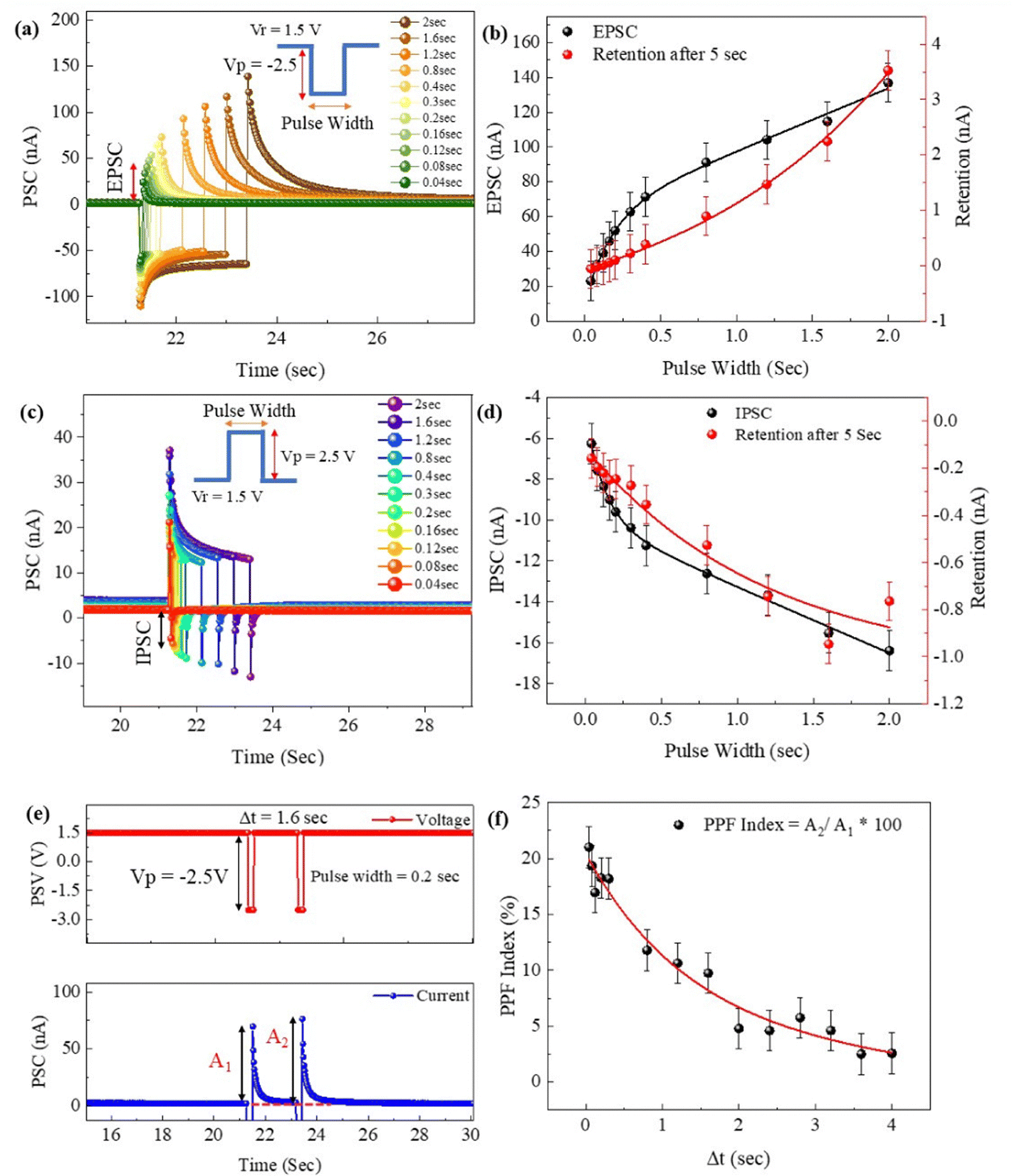 | ||
| Fig. 5 Electrical synaptic measurements performed using Au/Cs3Cu2I5/Au devices. (a) EPSC measured after applying the electrical pulses of different pulse width are applied. The read voltage (Vr = 1.5 V) and pulse voltage (Vp = −2.5 V). (b) Dependence of EPSC and the retained memory (residual EPSC) measured 5 s after the electrical pulse is switched off (Vp = −2.5 V). (c) Single pulse measurements were conducted with varying pulse widths, with positive pulse voltage (Vp = 2.5 V) and read voltage (Vr = 1.5 V), which results in inhibitory postsynaptic current (IPSC). (d) Dependence of IPSC and retained memory (residual IPSC). (e) PPF measurement performed by applying two consecutive voltage pulses of the same amplitude (Vp = −2.5 V) and pulse width (0.2 s) with varying pulse-to-pulse separation time Δt. (f) Variation of PPF index (A2/A1) × 100 with various Δt. | ||
The phenomenon of inducing inhibitory postsynaptic current (IPSC) and excitatory postsynaptic current (EPSC) through positive and negative electrical pulses can be due to the capturing and release of electrons at the trap levels of the Cs3Cu2I5/Au interface and also iodine vacancies within the perovskite halide.68,69
Short-term synaptic plasticity is one of the crucial measurements in neuromorphic computing applications, which involves transient synaptic events lasting from hundreds to thousands of milliseconds after pre-synaptic activity. It significantly influences brain functions like motion control and speech recognition. Paired-pulse facilitation (PPF) is a key form of this short-term plasticity, where we apply two consecutive voltage pulses and the synaptic strength is compared between the two pulses. From the biological synapse point of view, the PPF will strengthen the neurotransmitter release. Analogous to that, PPF can be emulated by applying two consecutive electrical pulses. The synaptic strength temporarily increases with two successive pulses i.e., (A2) is greater than (A1). The PPF index, calculated as [(A2/A1) × 100%] where A2 and A1 are the amplitudes of the second and first current peaks, respectively, measures this facilitation. Fig. 5(e) shows the response to two negative voltage spikes (0.2 s pulse width, 1.2 s separation). The upper panel shows the pulse voltages applied and the lower panel is the EPSC response measured. Clearly, there is a temporal coupling that exists thereby showing an increase in the synaptic weight. It has been established that the synaptic weight update depends on the time interval (Δt) between the presynaptic pulses. As shown in Fig. 5(f), the PPF index shows a gradual decay as Δt increases. The PPF decay can be explained using the following exponential decay function:
| PPF = 1 + A1exp(−t/τ1) + A2exp(−t/τ2) | (1) |
To check the electric pulse induced enhancement of the synaptic weight update, we conducted SRDP measurements by varying several electrical voltage pulse parameters, including the rate or frequency of firing a spike, number of pulses applied and pulse amplitude. We have performed all these measurements by using negative pulse voltage as it gave us EPSC. We maintained a constant pulse voltage amplitude (Vp = −2.5 V) while varying the firing rate by applying a train of 10 consecutive pulses in each cycle. This time, we increased the frequency of applied pulses as 2 Hz, 2.5 Hz, 3.3 Hz, 5 Hz, and 7.1 Hz, as illustrated in the top panel of Fig. 6(a). The lower panel shows the measured postsynaptic current. We define A1 and A10 as the EPSC amplitudes for the first and the 10th electric pulse. Here also, when the pulse train was applied at lower frequency (say 2 Hz), the change in the synaptic current is very small indicating a very small synaptic gain. When the spike frequency is increased to 7.1 Hz, we clearly see a synaptic gain in the device. The first pulse generated an EPSC of ∼63 nA (A1) and 10th pulse generated EPSC of ∼101.5 nA (A10), respectively. This shows an SRDP gain (A10/A1) ∼ 1.6. For all the spike frequency dependent SRDP measurements shown in Fig. 6(b), we obtained a gain indicating that the device can be operated to get a potentiation at various frequencies indicating suitability in the neuromorphic application.
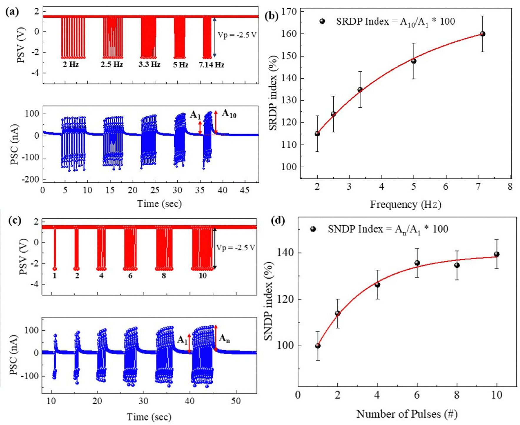 | ||
| Fig. 6 Multiple pulse measurements performed using Vp = −2.5 V. (a) SRDP measurements done by applying 10 consecutive voltage spikes of the same pulse width. (b) Dependence of SRDP index (A10/A1) × 100 on the frequency of application of pulses. (c) SNDP measurements performed by increasing the number of pulses (n = 1, 2, 4,…, 10). (d) Dependence of SNDP index (An/A1) × 100 with pulse numbers. | ||
Similar to the SRDP index, which indicates the spike frequency dependent synaptic amplification, we can induce synaptic weight modulation by increasing the number of constant voltage spikes. This is termed spike-number dependent plasticity (SNDP). A transition from STP to LTP can also be attained by SNDP.71 The upper panel in Fig. 6(c) shows that the number of voltage pulses applied increased in every cycle. The corresponding synaptic current measured is shown in the lower panel. Clearly, the number of spikes has a prominent effect on the synaptic weight update and SNDP index defined as (An/A1), where n is the number of voltage pulses applied in each cycle. The SNDP index exponentially increases indicating a strong potentiation in our devices. The results of the lower panel of Fig. 6(c) can be compared to the biological synapse where the repeated action potentials result in a higher concentration of neurotransmitters in the synaptic cleft, which increases ion flux through the post-synaptic membrane in a biological neuron. This synaptic capacity is regulated by adjusting the number of ions escaping to and accumulating at the Au/Cs3Cu2I5 synapses, a change validated by SNDP. The synaptic weight of an Au/Cs3Cu2I5 synapse exhibits a marked increase as the number of spikes rises from 1 to 10 (shown in Fig. 6(d)). Then, we performed SVDP measurement by varying the amplitude of the pulse from −2.5 V to −4 V, as shown in Fig. S3(a) (ESI†). Modifying the pulse amplitude can affect the degree of synaptic weight change. In Fig. S3(b) (ESI†), we observe that the post-synaptic current (PSC) increases with increasing voltage amplitude. By systematically optimizing these parameters, we can get valuable insights into the mechanisms underlying synaptic plasticity and optimize the conditions to achieve desired synaptic amplification.
4 Conclusions
In summary, we have synthesized lead-free, non-toxic Cs3Cu2I5 halide perovskite powder using a simple solid-state reaction with CsI and CuI and successfully fabricated a low power (pJ) consuming, two terminal, optoelectronic, artificial synapse using an Au electrode and Cs3Cu2I5 as the active material. With the smallest pulse of 80 ms, we found that the pulse energy/spike is about 1.36 pJ which could be tuned to even smaller energy consumption/spike. Our devices exhibited excellent memory capabilities. The read, write, and erase cycles maintained a highly stable high resistance state (HRS) and low resistance state (LRS) for over 8000 cycles, with clear ON–OFF states differing by a ratio of about 9. The MHP device also demonstrated impressive learning and forgetting properties, and the proposed device was stimulated using optical spikes in the UV region and electrical voltage spikes (both positive and negative) and it could mimic several crucial biological synaptic functions like EPSC, IPSC, PPF, SNDP, SRDP, and STM to LTM transition behavior, which are essential for developing artificial synapses for low-energy neuromorphic computing systems that operate at room temperature.Author contributions
A. B. M. and M. S.: conceptualization, data curation, formal analysis, investigation, visualization, writing – original draft, writing – reviewing and editing; R.T.: conceptualization, methodology, project administration resources, supervision, validation, visualization, writing – original draft, writing – reviewing and editing.Data availability
Data for this article, including figures are available at HARWARD Dataverse at DOI: https://doi.org/10.7910/DVN/S5G2TW.Conflicts of interest
There are no conflicts to declare.Acknowledgements
A. B. M. and M. S. would like to thank the Centre for Functional Materials (CFM), Vellore Institute of Technology for their support during this research work. R. Thamankar acknowledges the Centre for Functional Materials for infrastructure and also the Core Research Grant (CRG/2022/005093) from the Science and Engineering Board (SERB), India. R. Thamankar would like to acknowledge Dr. Ramakrishnan Ganesan, BITS PILANI, Hyderabad campus for the support in XPS measurements.References
- M. S. Hadj Sassi, F. G. Jedidi and L. C. Fourati, Procedia Comput. Sci., 2019, 159, 534–543 Search PubMed.
- M.-K. Kim, Y. Park, I.-J. Kim and J.-S. Lee, iScience, 2020, 23, 101846 CrossRef CAS PubMed.
- S. Choi, J. Yang and G. Wang, Adv. Mater., 2020, 32 Search PubMed.
- S. H. Jo, T. Chang, I. Ebong, B. B. Bhadviya, P. Mazumder and W. Lu, Nano Lett., 2010, 10, 1297–1301 CrossRef CAS PubMed.
- S. Jiang, S. Nie, Y. He, R. Liu, C. Chen and Q. Wan, Mater. Today Nano, 2019, 8, 100059 CrossRef.
- D. S. Jeong, K. M. Kim, S. Kim, B. J. Choi and C. S. Hwang, Adv. Electron. Mater., 2016, 2, 1600090 CrossRef.
- K. Liao, P. Lei, M. Tu, S. Luo, T. Jiang, W. Jie and J. Hao, ACS Appl. Mater. Interfaces, 2021, 13, 32606–32623 CrossRef CAS.
- Y. Lee and T.-W. Lee, Acc. Chem. Res., 2019, 52, 964–974 CrossRef CAS PubMed.
- B. Mu, H.-H. Hsu, C.-C. Kuo, S.-T. Han and Y. Zhou, J. Mater. Chem. C, 2020, 8, 12714–12738 RSC.
- I. Krauhausen, C.-T. Coen, S. Spolaor, P. Gkoupidenis and Y. van de Burgt, Adv. Funct. Mater., 2024, 34, 2307729 Search PubMed.
- L. Qiang, Y. Ni, L. Liu, L. Sun, J. Liu and X. Wen-Tao, Acta Phys. Sin., 2022, 71 Search PubMed.
- R. Singh, M. Kumar, S. Iqbal, H. Kang, J.-Y. Park and H. Seo, Appl. Surf. Sci., 2021, 536, 147738 Search PubMed.
- M. M. Islam, A. Krishnaprasad, D. Dev, R. Martinez-Martinez, V. Okonkwo, B. Wu, S. S. Han, T.-S. Bae, H.-S. Chung, J. Touma, Y. Jung and T. Roy, ACS Nano, 2022, 16, 10188–10198 CrossRef CAS PubMed.
- G. Lee, J.-H. Baek, F. Ren, S. J. Pearton, G.-H. Lee and J. Kim, Small, 2021, 17, 2100640 Search PubMed.
- Y. Wang, Z. Lv, Q. Liao, H. Shan, J. Chen, Y. Zhou, L. Zhou, X. Chen, V. A. L. Roy, Z. Wang, Z. Xu, Y.-J. Zeng and S.-T. Han, Adv. Mater., 2018, 30, 1800327 CrossRef.
- J. Gong, H. Wei, J. Liu, L. Sun, Z. Xu, H. Huang and W. Xu, Matter, 2022, 5(5), 1578–1589 CrossRef.
- X. Huang, Q. Li, W. Shi, K. Liu, Y. Zhang, Y. Liu, X. Wei, Z. Zhao, Y. Guo and Y. Liu, Small, 2021, 17, 2102820 CrossRef CAS.
- R. Roccanova, A. Yangui, G. Seo, T. D. Creason, Y. Wu, D. Y. Kim, M.-H. Du and B. Saparov, ACS Mater. Lett., 2019, 1, 459–465 Search PubMed.
- Z. Guo, J. Li, R. Pan, J. Cheng, R. Chen and T. He, Nanoscale, 2020, 12, 15560–15576 Search PubMed.
- A. K. Pramod, S. S. Kushvaha and S. K. Batabyal, J. Alloys Compd., 2024, 1006, 176320 Search PubMed.
- L. M. Herz, J. Phys. Chem. Lett., 2018, 9, 6853–6863 CrossRef CAS PubMed.
- F. Zu, D. Shin and N. Koch, Mater. Horiz., 2022, 9, 17–24 RSC.
- Y.-H. Kim, H. Cho and T.-W. Lee, Proc. Natl. Acad. Sci. U. S. A., 2016, 113, 11694–11702 CrossRef CAS PubMed.
- J. Shamsi, A. S. Urban, M. Imran, L. De Trizio and L. Manna, Chem. Rev., 2019, 119, 3296–3348 Search PubMed.
- S. A. Veldhuis, P. P. Boix, N. Yantara, M. Li, T. C. Sum, N. Mathews and S. G. Mhaisalkar, Adv. Mater., 2016, 28, 6804–6834 Search PubMed.
- H. Kim, J. S. Han, J. Choi, S. Y. Kim and H. W. Jang, Small Methods, 2018, 2, 1700310 CrossRef.
- C. He and X. Liu, Light: Sci. Appl., 2023, 12, 15 CrossRef CAS.
- H. Tsai, H.-H. Huang, J. Watt, C.-H. Hou, J. Strzalka, J.-J. Shyue, L. Wang and W. Nie, Adv. Sci., 2022, 9, 2105850 CrossRef CAS PubMed.
- R. A. John, Y. Demirağ, Y. Shynkarenko, Y. Berezovska, N. Ohannessian, M. Payvand, P. Zeng, M. I. Bodnarchuk, F. Krumeich, G. Kara, I. Shorubalko, M. V. Nair, G. A. Cooke, T. Lippert, G. Indiveri and M. V. Kovalenko, Nat. Commun., 2022, 13, 2074 CrossRef CAS.
- S. Han, L. Zhou, J. Huang, Y. Mu, Y. Xie and S. Zhou, ACS Appl. Electron. Mater., 2024, 6, 514–522 CrossRef CAS.
- C. C. Li, T. Yu Huang, Y. H. Lai, Y. C. Huang and C. Shan Tan, Mater. Today Electron., 2024, 8, 100095 CrossRef.
- P. Yang, G. Liu, B. Liu, X. Liu, Y. Lou, J. Chen and Y. Zhao, Chem. Commun., 2018, 54, 11638–11641 RSC.
- H. Shankar, A. Jha and P. Kar, Mater. Adv., 2022, 3, 658–664 Search PubMed.
- T. Krishnamoorthy, H. Ding, C. Yan, W. L. Leong, T. Baikie, Z. Zhang, M. Sherburne, S. Li, M. Asta, N. Mathews and S. G. Mhaisalkar, J. Mater. Chem. A, 2015, 3, 23829–23832 RSC.
- I. Kopacic, B. Friesenbichler, S. F. Hoefler, B. Kunert, H. Plank, T. Rath and G. Trimmel, ACS Appl. Energy Mater., 2018, 1, 343–347 Search PubMed.
- Y. Yang, C. Liu, M. Cai, Y. Liao, Y. Ding, S. Ma, X. Liu, M. Guli, S. Dai and M. K. Nazeeruddin, ACS Appl. Mater. Interfaces, 2020, 12, 17062–17069 CrossRef CAS PubMed.
- Z. Jin, Z. Zhang, J. Xiu, H. Song, T. Gatti and Z. He, J. Mater. Chem. A, 2020, 8, 16166–16188 RSC.
- G. Dai, Z. Ma, Y. Qiu, Z. Li, X. Fu, H. Jiang and Z. Ma, Inorg. Chem., 2022, 61, 12635–12642 CrossRef CAS PubMed.
- H.-F. Ni, L.-K. Ye, P.-C. Zhuge, B.-L. Hu, J.-R. Lou, C.-Y. Su, Z.-X. Zhang, L.-Y. Xie, D.-W. Fu and Y. Zhang, Chem. Sci., 2023, 14, 1781–1786 Search PubMed.
- M. Khawla, A. Dhouha, D. Ikram, E. Slim, O. Ali and E. Zakaria, Mater. Res. Bull., 2023, 167, 112396 Search PubMed.
- M. M. Byranvand, W. Zuo, R. Imani, M. Pazoki and M. Saliba, Chem. Sci., 2022, 13, 6766–6781 Search PubMed.
- M. L. Ali, M. Khan, M. A. Al Asad and M. Z. Rahaman, Heliyon, 2023, 9, e18816 CrossRef CAS PubMed.
- Y. Hui, S. Chen, R. Lin, W. Zheng and F. Huang, Mater. Chem. Front., 2021, 5, 7088–7107 RSC.
- X. Li, L. Zhang, Q. Zheng, Z. Zhou, S. He, D. Tian, A. Guo, C. Wang, S. Liu, X. Chu, C. Yang and F. Zhao, ACS Appl. Nano Mater., 2022, 5, 917–924 CrossRef CAS.
- Z. Zhao, X. Li, L. Xie, B. Chen, T. Jiang, J. Cao, F. Zhang, M. Wang, Y. Wu, H. Zheng, F. Zhang and Y. Wang, J. Lumin., 2022, 241, 118482 CrossRef CAS.
- C.-X. Li, S.-B. Cho, D.-H. Kim and I.-K. Park, Chem. Mater., 2022, 34, 6921–6932 CrossRef CAS.
- X. Wang, Y. Zhang, J. Zou, Z. Han, R. Chen, J. Li and Y. Zou, Opt. Mater., 2023, 143, 114168 CrossRef CAS.
- K. Zhang, S. Wang and L. Yi, J. Lumin., 2023, 254, 119516 CrossRef CAS.
- B. Sun, Y. Chen, M. Xiao, G. Zhou, S. Ranjan, W. Hou, X. Zhu, Y. Zhao, S. A. T. Redfern and Y. N. Zhou, Nanoletters, 2019, 19, 6461 CrossRef CAS.
- X. He, Y. Deng, D. Ouyang, N. Zhang, J. Wang, A. A. Murthy, I. Spanopoulos, S. M. Islam, Q. Tu, G. Xing, Y. Li, V. P. Dravid and T. Zhai, Chem. Rev., 2023, 123, 1207–1261 CrossRef CAS.
- W. Fu, L. Liu, G. Yang, L. Deng, B. Zou, W. Ruan and H. Zhong, Part. Part. Syst. Charact., 2015, 32, 907–914 CrossRef CAS.
- S. Zhu, B. Sun, S. Ranjan, X. Zhu, G. Zhou, H. Zhao, S. Mao, H. Wang, Y. Zhao and G. Fu, APL Mater., 2019, 7, 081117 CrossRef.
- B. Sun, M. Xiao, G. Zhou, Z. Ren, Y. Zhou and Y. Wu, Mater. Today Adv., 2020, 6, 100056 CrossRef.
- T. Kim, D. Lee, J. Kim and H. Sohn, Appl. Phys. Express, 2020, 13, 045003 CrossRef CAS.
- X. Zhang, M. E. Turiansky, J.-X. Shen and C. G. Van de Walle, Phys. Rev. B, 2020, 101, 140101 CrossRef CAS.
- J. Zhang, X. Zhang, M. E. Turiansky and C. G. Van de Walle, PRX Energy, 2023, 2, 013008 CrossRef.
- S. Lee, S. Wolfe, J. Torres, M. Yun and J.-K. Lee, ACS Appl. Mater. Interfaces, 2021, 13, 27209–27216 CrossRef CAS.
- Y. Sun, M. Tai, C. Song, Z. Wang, J. Yin, F. Li, H. Wu, F. Zeng, H. Lin and F. Pan, J. Phys. Chem. C, 2018, 122, 6431–6436 CrossRef CAS.
- F. Cao, T. Yan, Z. Li, L. Wu and X. Fang, Adv. Opt. Mater., 2022, 10, 2200786 CrossRef CAS.
- J. Ma, X. Xia, S. Yan, Y. Li, W. Liang, J. Yan, X. Chen, D. Wu, X. Li and Z. Shi, ACS Appl. Mater. Interfaces, 2021, 13, 15409–15419 CrossRef CAS PubMed.
- H. Shao, Y. Li, J. Zhuang, Y. Ji, X. He, R. Wang, L. Wang, J. Fu, W. Li, M. Yi, L. Xie, W. Huang and H. Ling, Adv. Funct. Mater., 2024, 34, 2316381 CrossRef CAS.
- L. Hu, J. Yang, J. Wang, P. Cheng, L. O. Chua and F. Zhuge, Adv. Funct. Mater., 2021, 31, 2005582 CrossRef CAS.
- J. Yang, L. Hu, L. Shen, J. Wang, P. Cheng, H. Lu, F. Zhuge and Z. Ye, Fundam. Res., 2024, 4, 158–166 CrossRef.
- L. Hu, J. Shao, J. Wang, P. Cheng, L. Zhang, Y. Chai, Z. Ye and F. Zhuge, Appl. Phys. Rev., 2024, 11, 011411 CAS.
- C. Zhu, H. Liu, W. Wang, L. Xiang, J. Jiang, Q. Shuai, X. Yang, T. Zhang, B. Zheng, H. Wang, D. Li and A. Pan, Light: Sci. Appl., 2022, 11, 337 CrossRef CAS.
- Z. Xie, D. Zhang, L. Cheng, C. Li, J. Elia, J. Wu, J. Tian, L. Chen, M. A. Loi, A. Osvet and C. J. Brabec, ACS Energy Lett., 2024, 9, 948–958 CrossRef CAS.
- Y. Li, Z. Shi, W. Liang, L. Wang, S. Li, F. Zhang, Z. Ma, Y. Wang, Y. Tian, D. Wu, X. Li, Y. Zhang, C. Shan and X. Fang, Mater. Horiz., 2020, 7, 530–540 RSC.
- Y. Yoon, Y. Kim, W. S. Hwang and M. Shin, Adv. Electron. Mater., 2023, 9, 2300098 CrossRef CAS.
- J. Li, D. Zhang, X. Li, S. Liu and F. Zhao, AIP Adv., 2024, 14, 035016 CrossRef CAS.
- H. K. Li, T. P. Chen, P. Liu, S. G. Hu, Y. Liu, Q. Zhang and P. S. Lee, J. Appl. Phys., 2016, 119, 244505 Search PubMed.
- B. Mandal, M. Raveendra Kiran and S. P. Singh, Mater. Adv., 2024, 5, 5179–5193 RSC.
Footnotes |
| † Electronic supplementary information (ESI) available. See DOI: https://doi.org/10.1039/d4ma00855c |
| ‡ These authors contributed equally to this work. |
| This journal is © The Royal Society of Chemistry 2025 |