
 Open Access Article
 This Open Access Article is licensed under a
 Creative Commons Attribution 3.0 Unported Licence
A solution processed metal-oxide:polymer interlayer improves the perovskite photodetector response speed, dark current, and stability†
Carlo A. R.
Perini
 *a,
Giorgio
Ferrari
b,
Juan-Pablo
Correa-Baena
ac,
Annamaria
Petrozza
d and
Mario
Caironi
*d
*a,
Giorgio
Ferrari
b,
Juan-Pablo
Correa-Baena
ac,
Annamaria
Petrozza
d and
Mario
Caironi
*d
aSchool of Materials Science and Engineering, Georgia Institute of Technology, Atlanta, GA 30332, USA. E-mail: carperini@gatech.edu
bDepartment of Physics, Politecnico di Milano, Milan, 20133 Italy
cSchool of Chemistry and Biochemistry, Georgia Institute of Technology, Atlanta, GA, 30332 USA
dCenter for Nano Science and Technology, Istituto Italiano di Tecnologia, Milan, 20134 Italy. E-mail: mario.caironi@iit.it
First published on 4th June 2025
Abstract
Metal halide perovskites (MHPs) are a promising class of solution processable materials for visible and near-infrared imaging, combining performances nearing those of commercial silicon detectors with a simpler processing. However, MHP photodiodes may suffer from poor stability, while challenges related to the thickness and uniformity of the interlayers used complicate deposition and reproducibility, often requiring the use of thermal evaporation. Here, we introduce a solution processable mixed electron transport layer (ETL) composed of zinc oxide (ZnO) nanoparticles blended with poly[(9,9-bis(3′-(N,N-dimethylamino)propyl)-2,7-fluorene)-alt-2,7-(9,9-dioctylfluorene)] (PFN). This hybrid interlayer combines the advantages of both metal oxide and organic transport layers, enabling fast, low-noise MHP photodiodes with promising stability, low hysteresis, and improved reproducibility. The mixed interlayer enables a dark current of 2.1 × 10⁻⁸ A cm−2 at −1 V bias, a white noise background below 6.5 × 10⁻¹⁴ A Hz−1/2 at −0.1 V, and an apparent specific detectivity of about 1012 Jones in the visible range. The device achieves a cutoff frequency (f−3dB) of 2.1 MHz for an area of 1.51 mm2, limited by its series resistance and capacitance, with further improvements possible through area reduction. Moreover, the ZnO:PFN interlayer enhances device shelf-life stability, maintaining nearly unchanged dark current over 570 days of aging. This work demonstrates the potential of mixed metal oxide–polymer interlayers for advancing MHP photodiodes toward practical, high-performance applications.
Broader contextMetal halide perovskites (MHPs) are leading materials for next-generation optoelectronics. However, MHP devices are limited by poor long-term stability and inefficient charge carrier extraction. Stability and charge collection can be improved via design of charge selective layers used to interface the MHP layer. Therefore, identifying suitable charge transport layers is crucial for advancing MHP optoelectronics. Among optoelectronic devices, photodetectors are the most impacted by the choice of transport layers. Photodetectors are devices that convert light into electricity, essential for applications such as communication, sensing, energy harvesting, and imaging. In this work, we introduce in a MHP photodetector an electron transporting layer (ETL) where metal oxide nanoparticles are mixed with an organic polymer. The mixed interlayer combines the advantages of organic and inorganic ETLs, enabling efficient electron transport, reduced non-radiative carrier recombination, improved rectification, long shelf-life, and improved reproducibility with respect to a metal oxide or an organic interlayer only, using a low-cost deposition process. These findings contribute to the broader effort of developing high-performance, stable, and scalable perovskite optoelectronics, with potential applications in photovoltaics, sensing, and imaging technologies. |
Introduction
The rapid advancement of technologies like Li-Fi and LIDAR has intensified the demand for photodetectors combining high detectivity, operation up to GHz frequencies, wavelength selectivity, low production costs, and ease of integration with read-out electronics.1–3 The range of potential applications spans from healthcare, to aviation, positioning systems, and vehicular and underwater communication.3 Conventional semiconductors like silicon suffer from increased noise and interference owing to their broad spectral response when used for light detection, imposing the need for more complex device designs.4,5 In this context, metal halide perovskite (MHP) photodetectors represent a promising alternative to conventional silicon-based devices, offering several unique advantages. These include simple fabrication methods, including large-area solution processing, tunable bandgaps that allow for customizable wavelength selectivity, reducing noise and unwanted responses to light, absorption coefficients higher than silicon, which allow films to absorb most of the incident light within a tenth of the thickness needed for silicon decreasing weights and increasing the maximum operational speeds, and high charge carrier mobilities that enable MHP photodetectors to achieve response at GHz frequencies.6–9MHP detectors have demonstrated specific detectivities (D*) exceeding 1012 Jones (i.e. cm Hz1/2 W−1), values which are comparable to those of commercial silicon detectors.7 At the same time, operational speeds in the GHz range have been shown.8–11 Some of the best MHP photodiodes cutoff frequencies (f−3dB) have been reported in the MHz range, which is to be ascribed to a high MHP dielectric constant, limiting the detector response in devices with an area of 1 mm2 as frequently used for testing in research labs, and to the use of interlayers with lower mobility than the perovskite film.10,12,13 MHz operational speeds with MHP photodiodes have been attained with strategies such as reducing the device area, or increasing the charge transport layer thickness to lower capacitance, with one report demonstrating GHz response speed using μm-sized pixels.8,10,11,14,15
Despite few exceptions, MHP photodiode architectures incorporate cathode buffer layers that need to be thinner than 10 nm not to impede charge extraction, bathocuproine (BCP) and lithium fluoride (LiF) being key examples.7,10,15–19 Thermal evaporation is generally used to enable deposition of such thin films with high uniformity, therefore limiting current leakage and resistive losses.10,15–17 The use of such thin layers imposes several challenges, including reduced device stability due to potential damage to the interlayer and underlying films during electrode deposition, limited protection of the perovskite film from moisture and oxygen and of the electrode from reaction with halide ions, and increased processing costs due to the strict thickness and uniformity requirements.20–23 A possible alternative to thermally evaporated interlayers involves using solution processed metal oxides in place of commonly used cathode buffer layers. Metal oxide films thicker than 150 nm can be deposited with low-cost solution techniques without compromising charge extraction, while also acting as barriers to halide, oxygen, and moisture permeation, thereby enhancing device stability.8,18,19 However, solution processed metal oxide nanoparticles are prone to aggregation in solution, which can reduce film coverage and uniformity, and suffer from a high density of surface defects.19 Both issues result in increased charge recombination and leakage, reducing the D* of the detector, and the overall stability. Consequently, the performances and stability of MHP photodiodes remain constrained by the lack of suitable interlayers.
In this work, we present a solution processed, mixed metal oxide nanoparticles:polymer electron transport layer (ETL) composed of a blend of ZnO with poly[(9,9-bis(3′-(N,N-dimethylamino)propyl)-2,7-fluorene)-alt-2,7-(9,9-dioctylfluorene)] (PFN), which combines the benefits of metal oxide and organic transport layers, to enable fast, low-noise perovskite photodiodes with low hysteresis, improved stability, and reproducibility. The mixed metal-oxide:polymer ETL reduces the leakage current with respect to a metal-oxide only film from 6.3 × 10⁻⁸ A cm−2 to 2.1 × 10⁻⁸ A cm−2 at −1 V bias, to a level that is comparable with currents attained with thermally evaporated ETLs such as BCP and LiF. A white noise background below 6.5 × 10⁻¹⁴ A Hz−1/2 is attained at −0.1 V, corresponding to an apparent specific detectivity  , computed assuming the responsivity does not change down to the measured noise background, of about 1012 Jones in the visible range. At the same time, the ZnO:PFN interlayer enables a measured f−3dB of 2.1 MHz for a device of 1.51 mm2 area, which remains limited by the device capacitance and could be improved by a further area reduction. The mixed interlayer improves the shelf-life stability of the detector with respect to organic cathode buffer layers, or metal oxides only, with the device retaining nearly unchanged dark current upon 570 days of aging.
Results and discussion
To benchmark the performances of the ZnO:PFN mixed metal oxide:polymer interlayer, we incorporated it in a photodiode device architecture comprising glass|indium-doped tin oxide (ITO)|poly(3,4-ethylenedioxythiophene):polystyrene sulfonate (PEDOT:PSS)|MHP (methylammonium lead triiodide)|phenyl-C61-butyric acid methyl ester (PC61BM)|metal oxide:polymer|Al, and compared it with a reference photodiode architecture we previously reported, which exploits Al-doped ZnO (AZO) as the interlayer, as schematically represented in Fig. 1a.8 | ||
| Fig. 1 a) Photodiode architecture selected to test the ZnO:PFN and AZO interlayers. (b) Dark J–V scans of the AZO and ZnO:PFN detectors acquired using a scan speed below 10 mV s−1. Both forward (Fw-solid line) and reverse (Rv-dashed line) bias scan directions are presented. (c) EQE (dashed line) and responsivity (solid line) of the AZO and ZnO:PFN detectors at 0 V bias. | ||
Blends of metal oxides and polymers have been previously incorporated in solar cell architectures, improving performances with respect to the individual materials.19 However, they have not been explored yet for MHP photodiode applications. Different combinations of metal oxides and polymers, as well as a small molecule, were pre-screened for this work (see Fig. S1, ESI†). Amongst the various combinations, ZnO:PFN and AZO were selected for further study as they provided the best combination of series (RS) and shunt (Rsh) resistance amongst all variations (see ESI Note 1 and Table S1†). Fig. 1b presents the absolute value of the current density versus applied voltage (J–V) for the ZnO:PFN and AZO diodes in the dark. Both J–V scans from negative to positive bias (Fw, solid lines) and from positive to negative (Rv, dashed lines) are presented in the plot, to account for hysteretic effects induced by ion motion and charge trapping.24 These effects can be particularly relevant at low current densities and can dominate the J–V in the dark.25 The overlapping curves in forward and reverse scan directions in Fig. 1b highlight negligible hysteresis in both detector architectures, which is promising as these dynamic effects can also impact the stability of the photodiodes output under illumination.26 Replacing the metal-oxide only AZO interlayer with ZnO:PFN reduces the dark current at −1 V from 6.3 × 10⁻⁸ A cm−2 to 2.1 × 10⁻⁸ A cm−2, slightly increases the slope in the diode-dominated region of the J–V scan reducing the ideality factor (n) from 1.25 to 1.09, and increases the current flowing at positive bias. The lower dark current at negative bias corresponds to an increased Rsh for the ZnO:PFN photodetector (51.3 MΩ cm2 against 17.2 MΩ cm2 for AZO). As a consequence, decreased shot and Johnson noise contributions are expected.27 The steeper slope in the diode-dominated region of the J–V curve (n closer to 1) is indicative of either reduced non-radiative recombination or interface-dominated non-radiative recombination at one of the interfaces,28 while the higher currents at positive bias reveal a decrease in the Rs from 14.3 to 6.7 Ω cm2. The values for these three parameters were retrieved from the J–V scans in the forward direction using the electrical equivalent model in Fig. S2a and the approximations discussed in ESI Note 2.† In Table S2† we summarize the values extracted from the fits in Fig. S2b and c.† The diode incorporating the ZnO:PFN interlayer enables a rectification ratio of 106 at (±1 V), with an improvement from the AZO detector reaching 105. The diode turn on voltage is changed to +0.45 V, from +0.50 V of the AZO one. This reduction in the Vth could indicate a deeper conduction band minimum for ZnO:PFN with respect to AZO.29 Previous work has shown improved uniformity of ZnO:PFN films with respect to metal oxide nanoparticles only.19 This is supported by the J–V data presented in Fig. S1,† where only 2 pixels out of 8 on the substrate are working for the AZO-interlayer detector, while 7 are working for the ZnO:PFN detector. The statistics for the J–V curves in the dark of both AZO and ZnO:PFN comprising detectors, presented in Fig. S3,† corroborate what was observed under illumination. At −1 V, the ZnO:PFN interlayer results in a lower average current of (4.04 ± 1.96) × 10−8 A cm−2, against (1.60 ± 1.15) × 10−7 A cm−2 for the AZO interlayer. Analogous reduction in standard deviation and average value is observed for the Rs, which is 9.6 ± 0.03 Ω cm2 for AZO, and 5.76 ± 0.01 Ω cm2 for ZnO:PFN. Overall, photodiodes incorporating the ZnO:PFN interlayer reveal lower average dark currents at reverse bias, lower Rs, and narrower standard deviation. Lastly, microscope images taken on our films, in Fig. S4,† reveal more uniform films, with less ‘comets’ due to defects when PFN is blended with the ZnO nanoparticles.30,31
To characterize the response of the photodiode under light we measure its responsivity (R) and use it to retrieve its external quantum efficiency (EQE), the two quantities being related by the formula:
 | (1) |
Following the static response of the detectors, we proceed to characterize their dynamic response. We begin by measuring the cutoff frequency (f−3dB) of a photodiode, defined as the frequency at which the photocurrent response to a sinusoidally modulated light input is decreased by 3 dB with respect to the static response. The cutoff frequency of perovskite photodetectors is often limited by their capacitance, which can be reduced by scaling down the area of the detector.8,10 To verify this, we characterize the response of photodiodes incorporating an AZO or a ZnO:PFN interlayer as a function of frequency and area, and present the results in Fig. 2a and b. For both detectors, reducing the area leads to an increased cutoff frequency. If the area is reduced by one order of magnitude, the f−3dB increases by approximately the same amount. For the AZO detectors the f−3dB increases from 0.2 MHz to 1.4 MHz as the area is reduced from 15.67 mm2 to 1.51 mm2. For the ZnO:PFN devices, f−3dB increases from 0.34 MHz to 2.1 MHz over the same change in area. The full comparison of cutoff frequencies as a function of area is provided in Table S3.† The statistics of the frequency response for the 1.51 mm2 ZnO:PFN detectors is reported in Fig. S5† with an average f−3dB of 1.77 ± 0.45 MHz. Despite the introduction of an insulating polymer blended into the nanoparticle layer in ZnO:PFN, no loss in operational frequency is seen with respect to the AZO device, with the ZnO:PFN devices showing a slightly higher cutoff frequency than the AZO detectors. The slightly faster response of the ZnO:PFN device is in agreement with the decrease in RS observed in these devices. These trends support an interpretation of the f−3dB in these detectors as dominated by the parasitic RS and capacitance of the detectors. We provide an extended discussion to support this conclusion in ESI Note 3 and Fig. S6.† Therefore, the f−3dB could be further increased by moving to even smaller area diodes, until the intrinsic response speed (ftr−3dB) of the diodes is reached, as it has been demonstrated in similar device configurations with f−3dB reaching up to the GHz range via area miniaturization.11,14,27
 | ||
| Fig. 2 Cutoff frequency as a function of area for a MHP photodetector incorporating an AZO interlayer (a) or a ZnO:PFN interlayer (b). (c) Photocurrent response of the detector incorporating ZnO:PFN to a train of rectangular 630 nm light pulses. (d) Comparison of dark currents and cutoff frequencies for photodiodes incorporating solution processed (blue dots) or evaporated interlayers (violet dots). The performances of the ZnO:PFN containing detector discussed in this work are marked with stars. Solid symbols denote detectors with dark current densities measured at −0.5 V; hollow symbols denote dark currents measured at −1 V. Data used for the plot are listed in Table S4.† | ||
Analogous to what was discussed in the case of dark currents, ion drift, diffusion, and charge carrier trapping can induce variations over time in the photoresponse of the detector.32 To understand whether such effects are at play in the response of diodes incorporating the ZnO:PFN interlayer, we study the stability of their response under illumination using a train of rectangular light pulses. As shown in Fig. 2c, the photocurrent output of a ZnO:PFN containing photodetector stabilizes within a few μs when the light is turned ON or OFF, and this response is reproducible over subsequent light pulses, returning each time to the same current levels in the dark and under illumination. In Fig. S7a† we show a zoom-in of a single pulse response and in Fig. S7b† the response of the detector under an extended train of light pulses. We note that the μs transients observed in this measurement are limited by the circuit response, as detectors of 15.67 cm2 area were characterized.
Overall, our photodetector demonstrates low dark currents combined with a high cutoff frequency, enabling performances that rival those of perovskites photodetectors comprising evaporated interlayers, and surpassing the performances of detectors comprising solely solution processed interlayers, as shown in Fig. 2d.
We continue to evaluate the benefits of incorporating the ZnO:PFN layer in MHP photodetectors by studying the response of the detector to varying incident optical power. This allows us to define the linear dynamic range (LDR) of the detector: the range of incident optical powers over which the R of the device remains constant. In photodiodes, the LDR can be limited at high illumination power intensities by the series resistance of the device and space-charge effects, while noise and non-radiative recombination processes dominate the response at low illumination. As visible in Fig. 3a, we are not able to measure the point at low light intensities at which the photoresponse deviates from linearity due to limitations in our experimental measurement setup. As such we define here the apparent LDR (LDRapp), expressed as
LDRapp = 20![[thin space (1/6-em)]](https://www.rsc.org/images/entities/char_2009.gif) log10(Imax,lin/Imin meas,lin), log10(Imax,lin/Imin meas,lin), | (2) |
 | ||
| Fig. 3 a) Photocurrent response as a function of incident optical power for the ZnO:PFN containing detector under illumination with a 450 nm laser mechanically chopped at 133 Hz. The linear fit (purple) highlights the range of linearity for the response of the photodiode. (b) Measured noise background of the ZnO:PFN photodetector (blue) at −0.1 V bias, predicted noise contributions (pink – shot noise, peach – Johnson noise, fuchsia – total estimated white noise), and measured noise contributions as a function of frequency (purple – 1/f noise, light gray – minimum noise). (c) Noise power at 20.0 Hz as a function of current flowing through the ZnO:PFN detector. (d) Range of apparent D* of the ZnO:PFN detector (blue). Lower bound is set by the SI@100Hz, while the upper bound is computed using the theory predicted values for white noise, attained as the sum of shot and Johnson noises. The gray area defines the range of D* typical of commercial silicon detectors. | ||
At low light intensities, the lowest signal that can be measured by the detector is limited by the detector noise. In a photodiode, noise comprises both frequency dependent (flicker noise) and frequency independent (white noise – e.g. shot noise and Johnson noise) components. The reduction in leakage current and the increased shunt resistance enabled by the use of ZnO:PFN as an interlayer are expected to reduce white noise, which would enable detection of lower power optical signals. In order to obtain experimental evidence of the actual noise of ZnO:PFN photodetectors, we proceeded to measure noise spectra using the setup described in Fig. S8.† We compare an estimate of the noise background of the setup in Fig. S9,† and the measured total noise spectrum of the device plus the setup, to determine the range of frequencies at which the noise background is dominated by the device under test (DUT). This limits our data discussion to frequencies below 100 Hz. We plot the photodiode noise in Fig. 3b, along with the theory-predicted shot noise and Johnson noise contributions. As visible in the experimental data, flicker noise, with its characteristic 1/f dependance, dominates the noise power spectrum (SI) at frequencies below 100 Hz. Flicker noise obeys the Hooge empirical relation:
 | (3) |
Having characterized noise and responsivity, we move to evaluate the specific detectivity of the ZnO:PFN detector. The specific detectivity of a planar photodiode can be defined as
 | (4) |
 :
: | (5) |
 is different from D*, as R will likely deviate from linearity at low enough incident optical powers. Our measurement represents a lower estimate of
  , as we are not able to access the true white noise power spectrum of the detector. Using the R from Fig. 1c, assuming SI@100Hz being equal to the white noise background, and operating the detector at a frequency above 100 Hz with a 1 Hz bandwidth, results in a
  above 5.0 × 1011 cm Hz1/2 W−1 in the 390–770 nm wavelength range, and reaching 1.2 × 10¹² Jones at 700 nm. An upper estimate of
  ,
,  can be defined assuming that the noise spectral power of the detector reaches the predicted white noise background at frequencies above 500 Hz, computed as the sum of shot and Johnson noises. In both cases, operation of the ZnO:PFN detector in the white noise dominated regime should be possible, benefiting from the frequency cutoff in the MHz range. The range of
  defined by these upper and lower boundaries is presented in Fig. 3d and compared to the D* of commercial silicon detectors in the visible range.
We conclude the characterization of ZnO:PFN as an interlayer for photodetectors by studying how the layer impacts the detector shelf-life stability. Devices comprising solely an organic top interlayer, as the PCBM|BCP combination commonly used for photodetectors, show a rapid degradation of the Al electrode (less than 1 day) upon exposure to air: bubbles and delaminated areas become visible on the electrode (Fig. 4a). Instead, when the ZnO:PFN interlayer is used, no change in the electrode appearance is observed, while a whitish-blue hue is visible on the aluminum surface immediately after deposition. The J–V characteristics of the ZnO:PFN-containing detector stored in a dark N2 environment, shown in Fig. 3d, reveal only a small change in the onset voltage of the diode upon storage for as long as 570 days (about 1 year and 6 months). The dark current at reverse bias is almost unchanged, which is different from what is observed in detectors comprising an AZO interlayer (Fig. S10†), and could be promising for commercial application of these detectors as changes in the dark current at reverse bias would affect the white noise background and thus D*. Based on these considerations, we propose the mixed organic:inorganic ZnO:PFN electron selective layer to enable the best device stability amongst the ETL combinations considered in this work.
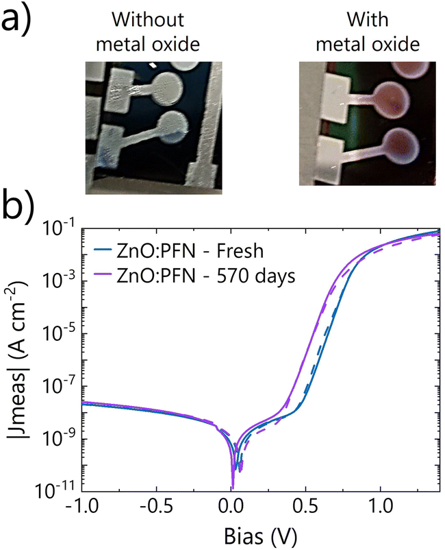 | ||
| Fig. 4 a) Pictures of detectors stored in air for a day. Detector comprising a PCBM|BCP ETL (left) showing corrosion vs. a ZnO:PFN ETL (right) where this reaction is hindered. (b) Shelf-life of a photodetector comprising the ZnO:PFN interlayer. J–V scans in the dark were acquired before and after storage in a N2 glovebox for 570 days. | ||
Conclusions
We have demonstrated a ZnO:PFN mixed organic–inorganic electron selective layer, which enables dark currents, response speeds, and stability superior to those of commonly used organic or inorganic materials. The ZnO:PFN interlayer enables a dark current of 2.1 × 10⁻⁸ A cm−2 at −1 V, an apparent D* above 5.0 × 1011 cm Hz1/2 W−1 in the visible range, a cutoff frequency of 2.1 MHz, and a shelf life stability longer than 1 year and 6 months, and it is easier to process in an interlayer than small molecules or metal oxides only. These characteristics make the ZnO:PFN interlayer a promising substitute to other cathode buffer layers currently in use.Data availability
The data supporting this article have been included as part of the ESI.†Conflicts of interest
There are no conflicts to declare.References
- Photodetectors for LiDAR – Hamamatsu, 2023..
- S. Rajbhandari, H. Haas, E. Xie, J. J. D. McKendry, J. Herrnsdorf, E. Gu, M. D. Dawson, D. O'Brien, H. Chun, G. Faulkner, K. Cameron, A. V. N. Jalajakumari, R. Henderson, D. Tsonev, M. Ijaz and Z. Chen, High-Speed Integrated Visible Light Communication System: Device Constraints and Design Considerations, IEEE J. Sel. Areas Commun., 2015, 33, 1750–1757 Search PubMed.
- S. Gupta, D. Roy, S. Bose, V. Dixit and A. Kumar, Illuminating the future: A comprehensive review of visible light communication applications, Opt. Laser Technol., 2024, 177, 111182 CrossRef.
- A. Beling and J. C. Campbell, High-Speed Photodiodes, IEEE J. Sel. Top. Quantum Electron., 2014, 20, 57–63 Search PubMed.
- C. So, W. J. Pyo and D. S. Chung, Advancements and Challenges of Vacuum-Processed Organic Photodiodes: A Comprehensive Review, Adv. Photonics Res., 2024, 6(2), 2400094 CrossRef.
- F. P. García de Arquer, A. Armin, P. Meredith and E. H. Sargent, Solution-processed semiconductors for next-generation photodetectors, Nat Rev Mater, 2017, 2, 16100 CrossRef.
- R. Ollearo, J. Wang, M. J. Dyson, C. H. L. Weijtens, M. Fattori, B. T. van Gorkom, A. J. J. M. van Breemen, S. C. J. Meskers, R. A. J. Janssen and G. H. Gelinck, Ultralow dark current in near-infrared perovskite photodiodes by reducing charge injection and interfacial charge generation, Nat. Commun., 2021, 12, 7277 CrossRef CAS PubMed.
- C. A. R. Perini, A. J. Barker, M. Sala, A. Petrozza and M. Caironi, High speed solution-processed hybrid perovskite photodetectors with low dark current enabled by a low temperature metal oxide interlayer, Semicond. Sci. Technol., 2018, 33, 094004 CrossRef.
- S. Yakunin, M. Sytnyk, D. Kriegner, S. Shrestha, M. Richter, G. J. Matt, H. Azimi, C. J. Brabec, J. Stangl, M. V. Kovalenko and W. Heiss, Detection of X-ray photons by solution-processed lead halide perovskites, Nat. Photonics, 2015, 9, 444–449 CrossRef CAS PubMed.
- Q. Lin, A. Armin, D. M. Lyons, P. L. Burn and P. Meredith, Low noise, IR-blind organohalide perovskite photodiodes for visible light detection and imaging, Adv. Mater., 2015, 27, 2060–2064 CrossRef CAS PubMed.
- A. Morteza Najarian, M. Vafaie, A. Johnston, T. Zhu, M. Wei, M. I. Saidaminov, Y. Hou, S. Hoogland, F. P. García de Arquer and E. H. Sargent, Sub-millimetre light detection and ranging using perovskites, Nat. Electron., 2022, 5, 511–518 CrossRef CAS.
- J. N. Wilson, J. M. Frost, S. K. Wallace and A. Walsh, Dielectric and ferroic properties of metal halide perovskites, APL Mater., 2019, 7, 010901 CrossRef.
- L. Dou, Y. M. Yang, J. You, W. Chang, G. Li, Z. Hong and Y. M. Yang, Solution-processed hybrid perovskite photodetectors with high detectivity, Nat. Commun., 2014, 5, 1–6 Search PubMed.
- A. P. Morozov, P. A. Gostishchev, A. Zharkova, A. A. Vasilev, A. E. Aleksandrov, L. O. Luchnikov, A. R. Tameev, D. A. Kiselev, T. S. Ilina, A. R. Ishteev, S. I. Didenko and D. S. Saranin, Micro-pixelated halide perovskite photodiodes fabricated with ultraviolet laser scribing, Appl. Phys. Lett., 2024, 124, 223503 CrossRef CAS.
- Y. Fang and J. Huang, Resolving weak light of sub-picowatt per square centimeter by hybrid perovskite photodetectors enabled by noise reduction, Adv. Mater., 2015, 27, 2804–2810 CrossRef CAS PubMed.
- Q. Lin, A. Armin, P. L. Burn and P. Meredith, Filterless narrowband visible photodetectors, Nat. Photonics, 2015, 9, 687–694 CrossRef CAS.
- C. Bao, Z. Chen, Y. Fang, H. Wei, Y. Deng, X. Xiao, L. Li and J. Huang, Low-Noise and Large-Linear-Dynamic-Range Photodetectors Based on Hybrid-Perovskite Thin-Single-Crystals, Adv. Mater., 2017, 29, 1–7 Search PubMed.
- T. Jiang and W. Fu, Improved performance and stability of perovskite solar cells with bilayer electron-transporting layers, RSC Adv., 2018, 8, 5897–5901 RSC.
- X. Jia, L. Zhang, Q. Luo, H. Lu, X. Li, Z. Xie, Y. Yang, Y. Q. Li, X. Liu and C. Q. Ma, Power Conversion Efficiency and Device Stability Improvement of Inverted Perovskite Solar Cells by Using a ZnO:PFN Composite Cathode Buffer Layer, ACS Appl. Mater. Interfaces, 2016, 8, 18410–18417 CrossRef CAS PubMed.
- C. Chen, S. Zhang, S. Wu, W. Zhang, H. Zhu, Z. Xiong, Y. Zhang and W. Chen, Effect of BCP buffer layer on eliminating charge accumulation for high performance of inverted perovskite solar cells, RSC Adv., 2017, 7, 35819–35826 RSC.
- J. Li, Q. Dong, N. Li and L. Wang, Direct Evidence of Ion Diffusion for the Silver-Electrode-Induced Thermal Degradation of Inverted Perovskite Solar Cells, Adv. Energy Mater., 2017, 7(14), 1602922 CrossRef.
- J. Yang, Q. Cao, T. Wang, B. Yang, X. Pu, Y. Zhang, H. Chen, I. Tojiboyev, Y. Li, L. Etgar, X. Li and A. Hagfeldt, Inhibiting metal-inward diffusion-induced degradation through strong chemical coordination toward stable and efficient inverted perovskite solar cells, Energy Environ. Sci., 2022, 15(5), 2154–2163 RSC.
- J. Hidalgo, W. Kaiser, Y. An, R. Li, Z. Oh, A.-F. Castro-Méndez, D. K. LaFollette, S. Kim, B. Lai, J. Breternitz, S. Schorr, C. A. R. Perini, E. Mosconi, F. De Angelis and J.-P. Correa-Baena, Synergistic Role of Water and Oxygen Leads to Degradation in Formamidinium-Based Halide Perovskites, J. Am. Chem. Soc., 2023, 145, 24549–24557 CAS.
- M. De Bastiani, G. Dell'Erba, M. Gandini, V. D'Innocenzo, S. Neutzner, A. R. S. Kandada, G. Grancini, M. Binda, M. Prato, J. M. Ball, M. Caironi and A. Petrozza, Ion migration and the role of preconditioning cycles in the stabilization of the J-V characteristics of inverted hybrid perovskite solar cells, Adv. Energy Mater., 2016, 6, 1–9 Search PubMed.
- W. Tress, J. P. Correa Baena, M. Saliba, A. Abate and M. Graetzel, Inverted Current–Voltage Hysteresis in Mixed Perovskite Solar Cells: Polarization, Energy Barriers, and Defect Recombination, Adv. Energy Mater., 2016, 6(19), 1600396 CrossRef.
- W. Tian, H. Zhou and L. Li, Hybrid Organic–Inorganic Perovskite Photodetectors, Small, 2017, 13(41), 1702107 CrossRef PubMed.
- S. Donati, Photodetectors: Devices, Circuits, and Applications, Meas. Sci. Technol., 2001, 12, 653 CrossRef.
- W. Tress, M. Yavari, K. Domanski, P. Yadav, B. Niesen, J. P. C. Baena, A. Hagfeldt, M. Graetzel, J. P. Correa Baena, A. Hagfeldt and M. Graetzel, Interpretation and evolution of open-circuit voltage, recombination, ideality factor and subgap defect states during reversible light-soaking and irreversible degradation of perovskite solar cells, Energy Environ. Sci., 2018, 11(1), 151–165 RSC.
- H. Seok, S. H. Kim, K. M. Yeom, J. H. Noh and H. Kim, Cost-Effective Transparent N-Doped Tin Oxide Electrodes with Excellent Thermal and Chemical Stabilities Enabling Stable Perovskite Photovoltaics Based on Tin Oxide Electron Transport Layer, Adv. Energy Mater., 2024, 14(13), 2303859 CrossRef CAS.
- K. Wang, N. Hohn, L. P. Kreuzer, T. Widmann, M. Haese, J.-F. Moulin and P. Müller-Buschbaum, Morphology Tuning of ZnO/P3HT/P3HT-b-PEO Hybrid Films Deposited via Spray or Spin Coating, ACS Appl. Mater. Interfaces, 2019, 11, 10998–11005 CrossRef CAS PubMed.
- A. C. Mendhe, in Simple Chemical Methods for Thin Film Deposition, Springer Nature Singapore, Singapore, 2023, pp. 387–424 Search PubMed.
- J. Bisquert, C. Gonzales and A. Guerrero, Transient On/Off Photocurrent Response of Halide Perovskite Photodetectors, J. Phys. Chem. C, 2023, 127, 21338–21350 CrossRef CAS.
- F. N. Hooge, T. G. M. Kleinpenning and L. K. J. Vandamme, Experimental studies on 1/f noise, Rep. Prog. Phys., 1981, 44, 479–532 CrossRef.
- F. N. Hooge, 1/f noise sources, IEEE Trans. Electron Devices, 1994, 41, 1926–1935 CrossRef CAS.
Footnote |
| † Electronic supplementary information (ESI) available. See DOI: https://doi.org/10.1039/d5el00043b |
| This journal is © The Royal Society of Chemistry 2025 |