
 Open Access Article
 This Open Access Article is licensed under a Creative Commons Attribution-Non Commercial 3.0 Unported Licence
Fluorinated fullerene interlayers for tin halide perovskite solar cells with enhanced operational air stability and minimized voltage losses†
Sergio
Galve-Lahoz
ab,
Jesús
Sánchez-Diaz
a,
Jorge
Marco-Guimbao
b,
Nihal
Guenani
a,
Jorge
Simancas
 a,
Jhonatan
Rodriguez-Pereira
cd,
Jesús
Lucia-Tamudo
e,
Sergio
Díaz-Tendero
fgh,
Jorge
Pascual
b,
Beatriz
Julián-López
a,
Juan P.
Martínez-Pastor
i,
Eva M.
Barea
a,
Iván
Mora-Seró
*a and
Juan Luis
Delgado
*bj
a,
Jhonatan
Rodriguez-Pereira
cd,
Jesús
Lucia-Tamudo
e,
Sergio
Díaz-Tendero
fgh,
Jorge
Pascual
b,
Beatriz
Julián-López
a,
Juan P.
Martínez-Pastor
i,
Eva M.
Barea
a,
Iván
Mora-Seró
*a and
Juan Luis
Delgado
*bj
aInstitute of Advanced Materials (INAM), University Jaume I, Av. Vicent Sos Baynat, s/n, 12071, Castellón de la Plana, Spain. E-mail: sero@uji.es
bPolymat, University of the Basque Country UPV/EHU, 20018 Donostia-San Sebastian, Spain. E-mail: juanluis.delgado@polymat.eu
cCenter of Materials and Nanotechnologies, Faculty of Chemical Technology, University of Pardubice, nám. Cs. legií 565, Pardubice, 53002, Czech Republic
dCentral European Institute of Technology, Brno University of Technology, Purkynova 123, Brno, 612 00, Czech Republic
eFaculty of Chemistry and Pharmacy, Institute of Physical and Theoretical Chemistry, University of Regensburg, 93040 Regensburg, Germany
fDepartment of Chemistry, Universidad Autónoma de Madrid, 28049, Madrid, Spain
gInstitute for Advanced Research in Chemistry (IAdChem), Universidad Autónoma de Madrid, 28049 Madrid, Spain
hCondensed Matter Physics Center (IFIMAC), Universidad Autónoma de Madrid, 28049 Madrid, Spain
iInstituto de Ciencia de los Materiales (ICMUV), Universitat de Valencia, 46980 Paterna, Spain
jIkerbasque, Basque Foundation for Science, Bilbao 48013, Spain
First published on 30th June 2025
Abstract
Tin halide perovskite solar cells (Sn-PSCs) are a promising alternative to their lead-based analogues due to their favorable optoelectronic properties. However, their performance is still limited by two main factors: on one hand, the tendency of Sn2+ to oxidize to Sn4+, which leads to high non-radiative recombination; and on the other hand, the offset between the perovskite conduction band and the LUMO level of the standard C60 fullerene, which hinders efficient charge transport and limits overall device performance. While the former has received significant attention, the latter has been less explored, despite being a major bottleneck for Sn-PSC development. In this work, we designed and synthesized two novel fullerene derivatives, namely JM10 and JM12, functionalized with different fluorine-rich moieties and incorporated them as interlayers between the perovskite and the C60 electron transport layer (ETL). These derivatives demonstrated suitable LUMO levels and effectively alleviated the energy level misalignment at the perovskite/ETL interface, minimizing the undesirable charge recombination and enhancing the charge extraction processes. As a result, the best-performing Sn-PSCs incorporating JM12 showed a nearly 20% increase in power conversion efficiency with respect to the reference devices. Moreover, the fluorinated groups increased the hydrophobicity of the interlayers, significantly improving the operational stability of the unencapsulated devices under harsh ambient conditions (60% RH and 25 °C). As a result, devices containing JM10 and JM12 retained up to 80% of their initial performance after more than 15 and 18 hours, respectively. These results highlight the potential of fullerene chemistry's versatility to mitigate carrier losses at the interfaces while simultaneously improving both the performance and stability of Sn-PSCs, paving the way for future advancements in their design and development.
Broader contextSince their emergence in 2009, lead-halide perovskite solar cells (PSCs) have shown great promise for high-efficiency, low-cost photovoltaics. However, concerns over lead toxicity have prompted efforts to develop safer alternatives. Tin-based perovskites (Sn-PSCs) stand out due to their favorable optoelectronic properties, but their efficiency and long-term stability still lag behind, largely due to suboptimal energy level alignment with standard electron transport materials like C60. While alternatives such as ICBA have improved photoconversion efficiency (PCE), they often compromise device stability. This work targets a key limitation in Sn-PSC performance by developing two novel fluorinated fullerene derivatives, JM10 and JM12, designed to improve energy alignment at the perovskite interface. Their incorporation as interlayers significantly enhances charge extraction, leading to PCE improvements of nearly 20%, and a sixfold increase in ambient stability for unencapsulated devices. These results represent an important step forward for lead-free PSCs, offering a promising route to safer and more stable solar energy technologies. |
Introduction
Since the first reported hybrid lead-halide perovskite solar cell (Pb-PSC) in 2009,1 these materials have shown an unprecedented potential to outperform conventional silicon-based solar cells and dominate the photovoltaic market.2–4 However, global regulations on lead as a hazardous material could hinder their commercialization.5–7 To overcome this issue, the scientific community started to focus on alternative materials, with Sn demonstrating to be the best candidate to replace Pb at the divalent cation site due to its outstanding optoelectronic properties.8,9 Nevertheless, the current record efficiencies achieved in Sn-PSCs still lag too far below the Shockley–Queisser theoretical limit efficiency (∼33%).10–13One of the main reasons behind this efficiency gap is related to the poor band alignment between the conduction band (CB) of the Sn-perovskite active layer and the lowest unoccupied molecular orbital (LUMO) level of the commonly used C60 ETL.14,15 Initially, C60 emerged as an effective ETL in Pb-PSCs due to its high charge mobility,16,17 but the shallower CB of Sn-PSCs leads to the aforementioned energy mismatch. Accordingly, inefficient charge extraction at the interface and serious open-circuit voltage (VOC) losses are usually observed.14 Nonetheless, the mixed sp2 and sp3 hybridization of the carbon atoms within the C60 cage not only confers high charge mobility to the layer,18,19 but also offers the possibility of raising the LUMO level of fullerene derivatives by disrupting their conjugated π systems through suitable cage functionalization.20–22 This tunability has enabled the successful incorporation of alternative fullerene derivatives, such as phenyl-C61-butyric acid methyl ester (PCBM) or indene-C60 bisadduct (ICBA), into Sn-PSCs as ETLs, yielding impressive VOC values approaching the Shockley–Queisser theoretical limit.11,23–25 However, reducing the conjugation within the cage notably decreases the electron mobility of the devices, thereby compromising the short circuit current density (JSC). For instance, Liang et al. studied different ETLs, including C60, PCBM and ICBA, in Pb-PSCs, and reported a significant decrease in the electron mobility across the fullerene layer, following the trend C60 > PCBM > ICBA (1.6 cm2 V−1 s−1 for C60, 6.1 × 10⁻² cm2 V−1 s−1 for PCBM, and 6.9 × 10⁻³ cm2 V−1 s−1 for ICBA), which subsequently influenced the JSC of the devices.17 Based on these observations, a promising strategy to address the energy level mismatch in Sn-PSCs, without leaving aside the excellent charge mobility offered by the C60 ETL, involves the incorporation of novel fullerene derivatives with appropriate LUMO levels as interlayers between the perovskite active layer and the advantageous C60.15,26,27
Another critical issue in Sn-PSCs lies in the fast oxidation of Sn2+ to the Sn4+ state in the presence of oxidizing agents, such as water or oxygen molecules, leading to device instability and posing serious issues for the reliable study and processing of these materials.28,29 To mitigate these degradation pathways, an interesting approach involves the development of new materials capable of physically isolating the perovskite layer without disrupting its electronic properties. In this context, fluorinated compounds have proven to be excellent moisture barriers due to their high hydrophobicity, significantly enhancing the air stability of different Pb-PSCs.30–32 Furthermore, the strong electronegativity of fluorine atoms allows them to interact with electron-deficient sites, such as I− vacancies, compensating charge deficiencies at the perovskite surface.33,34 However, despite these promising characteristics, the potential of fluorinated compounds in Sn-PSCs remains largely unexplored, presenting a significant opportunity for future research.35,36
Herein, we decided to leverage the chemical versatility of fullerenes, which can be tailored with different functional groups to achieve desirable chemical and electronic properties. Specifically, we designed and synthesized two novel fullerene derivatives functionalized with different fluorine-rich moieties, namely JM10 and JM12, and incorporated them as interlayers in Sn-PSCs. These interlayers optimized the energy level alignment between the CB of the perovskite and the LUMO level of C60, as we characterized experimental and theoretically, boosting the VOC and raising the power conversion efficiency (PCE) of the devices. In this way, JM10 with a pentafluorobenzene unit showed an increased in the device efficiency to 10.5%, while JM12 incorporated a 3,5-bis(trifluoromethyl)phenyl group and further boosted the efficiency to 11.0%, compared to 9.4% for the control devices, representing a 17% increase of performance. Furthermore, unencapsulated devices incorporating the interlayers presented an enhanced operational stability in air (60% RH and 25 °C), retaining up to 80% of their initial PCE after more than 15 and 18 hours of continuous operation for JM10 and JM12 fullerenes, respectively, while the control devices degraded after 3 hours of operation.
Results and discussion
In this study, we designed and synthesized two novel [60]fulleropyrrolidines through a one-step 1,3-dipolar cycloaddition of different azomethine ylides to the C60 precursor, that have been also theoretically simulated, see below. This reaction, also known as Prato reaction,37,38 is widely used for the functionalization of fullerenes, as it allows for the straightforward attachment of different substituents to the fullerene cage. [60]Fulleropyrrolidines usually exhibit lower electron affinity than pristine C60 fullerene or other derivatives, a property directly correlated with higher LUMO values.20,39,40 As Sn-based perovskites present shallower CBs than their Pb-based counterparts, [60]fulleropyrrolidines are perfect candidates for fixing the inadequate band alignment at this interface.41 Furthermore, both fullerene derivatives were functionalized with different fluorinated aromatic rings, and an n-butyl alkyl chain attached to the N atom of the pyrrolidine moiety. We anticipated that the fluorinated rings would enhance the hydrophobicity and the dipolar moment of the layer, thereby ensuring a better electron extraction, while the alkyl chain would increase the solubility of the fullerenes in non-polar solvents such as chlorobenzene. In this way, JM10 presented a pentafluorophenyl unit and JM12 incorporated a 3,5-bis(trifluoromethyl)phenyl group. The synthetic route is depicted in Scheme S1,† and the molecular structures are confirmed through nuclear magnetic resonance (1H NMR, 13C NMR and 19F NMR) and mass spectrometry (MS), see Fig. S1–S8.† Further synthetic details are provided in the ESI.†To evaluate the suitability of the synthesized materials, and their effectiveness to improve the charge extraction from the perovskite to the ETL, cyclic voltammetry (CV) experiments were conducted to determine their LUMO energy levels. The comparison of CV spectra is presented in Fig. 1a, where both JM10 and JM12 exhibited lower electron-accepting abilities compared to C60, as indicated by their more negative half-wave potential values. The LUMO energy levels were estimated to be −4.05 eV, −3.98 eV and −4.01 eV for C60, JM10 and JM12, respectively. The higher LUMO levels observed in both fullerene derivatives demonstrated their potential to enhance the charge extraction from the perovskite's CB to the ETL selective contact in Sn-PSCs. Additionally, the optical properties of the fullerene derivatives were analyzed using UV-vis absorption spectroscopy, see Fig. 1b. Fullerenes typically exhibit strong absorptions in the UV region, below 350 nm, associated to the typical π–π* transitions in aromatic systems.42 The sharp peak at 430 nm observed for both JM10 and JM12 is attributed to the saturation of a double bond in the fullerene cage, confirming the formation of a 58 π-electron system.43 Moreover, both JM10 and JM12 presented a notorious redshift compared to pristine C60, see inset in Fig. 1b, which is ascribed to the extended overall π-conjugation along the pyrrolidine and fluorinated moieties.44 As a result, a reduction in the energy gaps between the HOMO and the LUMO levels was obtained. The bandgaps Eg were estimated from the onset of the absorption, and the HOMO levels were calculated from EHOMO = ELUMO − Eg. All the parameters are summarized in Table S1† and the estimated energy levels are represented in Fig. 1c.
 | ||
Fig. 1 (a) CV of C60, JM10, and JM12 in acetonitrile![[thin space (1/6-em)]](https://www.rsc.org/images/entities/char_2009.gif) :o-dichlorobenzene (1:4) (NBu4+PF6− 0.1 M was employed as supporting electrode) vs. Fc/Fc+ couple, dotted line is an eye guide. (b) UV-vis absorption spectra of the fullerene derivatives in chlorobenzene (1 × 10⁻⁵ M). (c) Schematic illustration of the LUMO levels for the different fullerene derivatives, extracted from (a) and conduction band of FASnI3 perovskite, extracted from ref. 45. (d) Molecular electrostatic potential at ρ = 0.001 a.u. Range of values of the electrostatic potential: from −0.01 (red) to 0.01 (blue). Black arrows indicate the net dipole moment direction. :o-dichlorobenzene (1:4) (NBu4+PF6− 0.1 M was employed as supporting electrode) vs. Fc/Fc+ couple, dotted line is an eye guide. (b) UV-vis absorption spectra of the fullerene derivatives in chlorobenzene (1 × 10⁻⁵ M). (c) Schematic illustration of the LUMO levels for the different fullerene derivatives, extracted from (a) and conduction band of FASnI3 perovskite, extracted from ref. 45. (d) Molecular electrostatic potential at ρ = 0.001 a.u. Range of values of the electrostatic potential: from −0.01 (red) to 0.01 (blue). Black arrows indicate the net dipole moment direction. | ||
To elucidate the differences in the molecular electronic distribution between both derivatives, we analyzed their electrostatic potential (ESP) distributions and calculated their dipole moments using density functional theory (DFT). The properties of the C60 fullerene and two hypothetical intermediate derivatives, JM8 and JM9, which progressively resemble the complexity of JM10 and JM12, were also investigated to better understand the contributions of the different molecular components within their structure, see Fig. 1d. Due to the high icosahedral symmetry, Ih, of C60, its net dipole moment, |μ|, is zero. However, the spatially extended electron cloud of C60 fullerene enhances its molecular polarizability, owing to degenerated, energetically accessible LUMO orbitals that readily accept electrons. These characteristics enable strong polarization upon the incorporation of electron-donating or electron-withdrawing groups, leading to the formation of intense permanent molecular dipoles. Thereby, as shown in Fig. 1d and Table S2,† the addition of an N-methyl pyrrolidine moiety to the C60 unit leads to the hypothetical JM8 molecule, which exhibits enhanced molecular polarization and a net dipole moment oriented along the direction of the substituent. This behavior arises from the electron-donating nature of the substituent, which increases the electronic density within the fullerene core (negative pole), while generating a positive pole at the substituent. Further functionalization with an aromatic ring yields JM9 molecule, featuring a slightly intensified dipole along the same direction, due to the additional group's electron-donating effect. Interestingly, replacing all hydrogen atoms on the aryl ring with fluorine atoms, JM10, reverses the direction of the molecular dipole. The strong electron-withdrawing nature of the fluorinated ring induces a dramatic change in the direction of the dipolar moment, but some components of the dipole moment are, however, canceled by opposite contributions from the fluorine atoms aligned in the same direction. In contrast, replacing the perfluorinated aryl ring with two meta-positioned –CF3 groups in the aryl ring, as in JM12, diminishes this neutralization effect, increasing the molecular polarization and resulting in the highest net dipole moment among all the studied derivatives. Based on the estimated dipole moments of the different fullerene derivatives, it is expected that the synthesized fullerene derivatives exhibit strong interactions with the surface of the ionic perovskite structure. These electrostatic interactions are likely to facilitate the surface passivation by occupying under-coordinated ions and reducing the vacancy defects. Thus, an effective reduction of the trap-state density at the perovskite/ETL interface is expected for JM10 and JM12, especially for the latest.46,47
To assess the impact of the interlayers deposition on the Sn perovskite film quality, X-ray diffraction (XRD) measurements and scanning electron microscopy (SEM) imaging were conducted, see Fig. S9 and S10.† The XRD patterns revealed two dominant peaks corresponding to the crystalline planes (100) and (200), indicating a clear preferential oriented growth along the (100) crystalline direction. The absence of any shift in the peak positions or significant changes in the full width at half-maximum (FWHM) values upon the interlayer deposition indicates that they do not disrupt the perovskite crystalline lattice. On the other hand, SEM images were taken at different magnifications and demonstrated the formation of uniform, pinhole-free layers with an average grain size exceeding 1 μm in diameter in all the cases. Low-magnification SEM images suggested the presence of some organic material on the perovskite layer, with a noticeable difference between the JM10 and JM12 layers. Specifically, the JM12 layer appeared more homogeneous, whereas the JM10 layer showed more isolated organic domains. Apart from these differences in the interlayer homogeneity, minimal variations in the perovskite film morphology were observed, thus confirming the interlayer's compatibility with the FASnI3 perovskite and the high quality of the resulting films. To further study the interlayers homogeneity, atomic force microscopy (AFM) images were conducted. As shown in Fig. 2a–c, the JM10 layer presented a non-uniform distribution with self-aggregate domains, whereas the JM12 layer displayed a smooth and regular structure. This discrepancy between both materials can be attributed to a higher packing degree in the JM10 layer, likely due to greater π–π stacking interactions.48,49
 | ||
| Fig. 2 AFM images of (a) FASnI3, (b) FASnI3/JM10 and (c) FASnI3/JM12 film surfaces. KPFM topography map of (d) FASnI3, (e) FASnI3/JM10 and (f) FASnI3/JM12 film surfaces. (g) PL spectra and (h) time-resolved PL decays corresponding to FASnI3/C60 films on glass substrate with and without top interlayers. | ||
A key limitation of Sn-PSCs is their voltage losses, mainly resulting from the non-radiative recombination and the misaligned energy levels at the top interface. The use of proper additives has significantly contributed to the reduction of bulk non-radiative recombination.10,29,50–52 However, energy level misalignment has received less attention. To evaluate the charge extraction ability of the fullerene derivatives, Kelvin Probe Force Microscopy (KPFM) measurements were carried out. Fig. 2d shows the KPFM map of the pristine perovskite film, where higher values in the potential difference are observed at the grain boundaries. These sites can easily trap charge carriers due to the presence of structural defects, hindering their mobility and complicating their extraction to the ETL.53,54 When the JM10 layer is incorporated, as shown in Fig. 2e, a clear increase in the overall surface potential difference is observed, especially in the areas where the presence of the organic material is more prominent. Conversely, upon the addition of the JM12 interlayer, a more uniform and complete perovskite coverage was obtained and the surface potential difference increased up respect both pristine and with JM10 incorporation, as shown in Fig. 2f. These notable increases in the surface potential difference can be ascribed to an electron transport from the perovskite layer to the JM12 fullerene derivative interlayer, demonstrating a huge potential to enhance the device performance, and confirming the difference in homogeneity between the organic layers previously commented.
To further explore the carrier dynamics and the interfacial recombination, steady-state photoluminescence (PL) and time-resolved photoluminescence (TRPL) spectroscopy measurements were performed for the FASnI3/C60, FASnI3/JM10/C60, and FASnI3/JM12/C60 samples. The PL spectra are shown in Fig. 2g, and a clear increase in PL intensity is observed upon the addition of both fullerene derivatives. A PL intensity enhancement is typically related to lower non-radiative recombination.55 This increase can be ascribed to an effective surface passivation, reducing the non-radiative recombination centers at the top perovskite interface. Note that, as these samples are measured in open-circuit conditions, there is no net electron transfer from the perovskite to the charge transport layers during the steady-state PL measurements. Thereby, the effectiveness of charge extraction at the contacts cannot be directly inferred from these measurements, as sometimes assumed in literature.56 However, in TRPL measurements, due to the transient nature of the technique substantial currents can flow to equilibrate the quasi-Fermi levels during the decay process. As a result, in addition to interface and bulk recombination, charge extraction processes must also be considered in TRPL experiments.57
The TRPL spectra are presented in Fig. 2h. PL decays have been fitted using a monoexponential decay function, obtaining average lifetimes (τave) of 3.25 ns, 3.67 ns and 2.50 ns for FASnI3/C60, FASnI3/JM10/C60, and FASnI3/JM12/C60, respectively. Interestingly, the trend observed in the steady-state PL between the sample with JM12 and the reference is now reversed, with the JM12 treated film showing a shorter τave. Considering that charge transport processes can occur in TRPL, the reduced τave observed for the sample with JM12 can be attributed to an improved charge extraction from the perovskite layer to JM12, while its higher steady-state PL emission indicates lower non-radiative recombination.
On the other hand, the FASnI3/JM10/C60 sample exhibited the longest τave among all the samples. Here the trade of between the decrease of non-radiative recombination observed by steady PL, that causes an increase of τave, and the increase of charge extraction, producing a decrease of τave, should be considered. Thus, when comparing JM10 and JM12, both showed similar enhanced PL intensities, but the longer τave displayed by JM10 suggests less efficient charge extraction than for JM12.
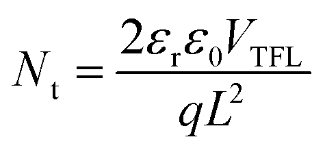
To assess the ability of the interlayers to reduce the trap-state density (Nt) in the perovskite film, we characterized the space-charge limited current (SCLC) of the devices.58,59 As electrons are minority carriers in p-doped Sn-based perovskites, we fabricated electron-only devices with the structure of ITO/SnO2/FASnI3/C60/BCP/Ag with and without the interlayers between perovskite and C60. The dark J–V curves are presented in Fig. S10.† Commonly, three different regions can be distinguished, such as the ohmic region at low voltages, the trap-filled limited (TFL) region at intermediate voltages, and the Child region at high applied voltages. The intersection point between the ohmic and the TFL regions represents the trap-filled limit voltage (VTFL), where all the available trap states are completely filled by the injected carriers. Accordingly, the Nt can be calculated from the following equation:
To further understand the chemical interactions behind the passivation mechanism of the perovskite surface by the interlayers, X-ray photoelectron spectroscopy (XPS) was performed. Changes in the local chemical environments of the different atoms present at the perovskite surface can be reflected through shifts in the binding energy peak positions. Fig. 3a shows the high-resolution Sn 3d XPS spectra, where the characteristic spin–orbit splitting of Sn 3d5/2 and Sn 3d3/2 is observed in the pristine FASnI3 perovskite, both with and without JM10 and JM12 interlayers. No significant shift in the binding energy of the Sn2+ components was detected in the presence of JM10, reflecting a weak interaction with the perovskite. In contrast, JM12 induced a small but still noticeable change in the electronic density distribution around the Sn nuclei, showing a higher downshift of 0.13 eV. A downshift in the binding energy implies an increased electron density around the Sn nucleus, suggesting that uncoordinated Sn2+ sites can be electronically compensated by the adsorption of JM12 molecules, thereby improving the charge distribution at the surface. Furthermore, the high-resolution N 1s XPS spectra were also analyzed and presented in Fig. 3b. In the pristine perovskite, a single component corresponding to FA+ cations (C![[double bond, length as m-dash]](https://www.rsc.org/images/entities/char_e001.gif) NH2+) was detected at 400.12 eV. Interestingly, this peak remained unchanged upon the addition of JM10, whereas it shifted to 400.00 eV after adding JM12 interlayer. Additionally, a new signal associated with C–NH2 was also detected at 398.96 eV and 398.86 eV for JM10 and JM12, respectively. The observed downshift suggests an effective charge compensation from the fullerenes to the formamidinium cations, while the detection of the new signals may be ascribed to a structural rearrangement or reorientation of the FA+ cations induced by the interaction with the fullerene derivatives.60
NH2+) was detected at 400.12 eV. Interestingly, this peak remained unchanged upon the addition of JM10, whereas it shifted to 400.00 eV after adding JM12 interlayer. Additionally, a new signal associated with C–NH2 was also detected at 398.96 eV and 398.86 eV for JM10 and JM12, respectively. The observed downshift suggests an effective charge compensation from the fullerenes to the formamidinium cations, while the detection of the new signals may be ascribed to a structural rearrangement or reorientation of the FA+ cations induced by the interaction with the fullerene derivatives.60
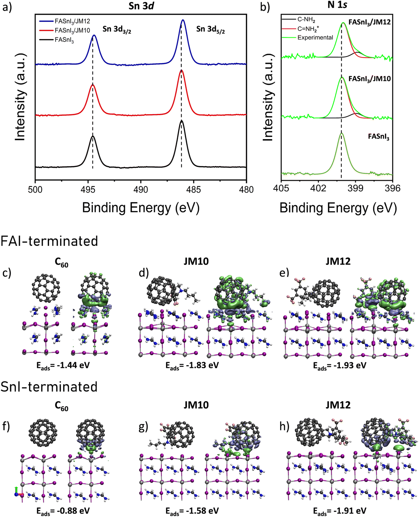 | ||
| Fig. 3 High-resolution XPS spectra of (a) Sn 3d and (b) N 1s for the perovskite films with and without JM10 and JM12 interlayers. Isosurface of Δρ = 0.002 a.u. for (c and f) FASnI3/C60, (d and g) FASnI3/JM10, and (e and h) FASnI3/JM12 systems with SnI2-terminated and FAI-terminated structures, respectively. Green and blue regions represent positive and negative values of Δρ, respectively. | ||
To validate this hypothesis, we performed DFT calculations to model the adsorption of the fullerene derivatives on different FASnI3 surfaces. We considered three distinct molecular orientations and two surface terminations, named SnI2-terminated and FAI-terminated, see Fig. S12.† Since Sn-based perovskite surfaces are prone to irregularities and defect states which lead to heterogeneous atomic structures along the whole surface, considering all these scenarios can provide a more comprehensive and insightful analysis. All the calculated adsorption energies are summarized in Table S3.† Regarding the molecular orientation of the [60]fulleropyrrolidines, the adsorption energy was notably higher when both the fluorinated moiety and the fullerene cage interacted simultaneously with the surface, suggesting a preferred molecular orientation with multiple anchoring points, as shown in Fig. S13 and S14.† This dual interaction notably enhanced the adsorption, especially on FAI-terminated surfaces. Moreover, JM12 exhibited higher adsorption energies than JM10 in all cases, indicating that increasing the polarity of the electron-withdrawing substituent may enhance the adsorption stability, see Fig. 1d and Table S3.†
A more detailed analysis of the electron density changes for the cases with higher adsorption energies (i.e., FAI-terminated surfaces and “middle” molecular orientations) showed an increase in electron density in the fullerene core for both in JM10 and JM12, as shown in Fig. 3c–e, where green and blue regions represent areas of electron accumulation and depletion, respectively. This change is accompanied by a depletion of electron density at the interface, mainly due to electron donation from the external iodide atoms to the fullerene cage. Meanwhile, the regions where the fluorinated substituents directly interact with the perovskite surface exhibit an increase in electron density, particularly in the case of JM12. Thus, the formamidinium cation in the surface layer attracts electron density from the –CF3 groups in the aryl ring, reflecting the formation of strong interactions as previously observed in the XPS analysis, see Fig. 3b. Interestingly, SnI2-terminated surfaces, where the external I atoms are missing, exhibited a different electron density redistribution upon molecular adsorption. As shown in Fig. 3f–h, an overall electron accumulation can be observed at the interface, compensating for the electron-deficient Sn sites and supporting the XPS results presented in Fig. 3a. Furthermore, although adsorption energies were stronger for FAI-terminated surfaces, the energy difference between JM10 and JM12 with C60 was significantly higher for SnI2-terminated surfaces, highlighting the role of the fluorinated moieties in compensating charge-deficient sites. These findings not only corroborate the experimental results, but also provide useful information about the role of different molecular moieties in the electronic redistribution at the perovskite surface in different scenarios.
To study the potential of the interlayers to improve the performance of Sn-PSCs, we fabricated devices with an inverted p–i–n configuration following the architecture: ITO/PEDOT:PSS/FASnI3/C60/BCP/Ag, where PEDOT:PSS is poly(3,4-ethylenedioxythiophene):polystyrene sulfonate and BCP is bathocuproine, see Fig. 4a. For the interlayer deposition, a 0.5 mM solution of JM10 or JM12 in chlorobenzene was dropped onto the perovskite film, see Fig. S15.† All the devices were exposed to a light-soaking treatment as part of a purification process, as previously reported by our group.29 The photovoltaic parameters, including JSC, VOC, fill factor (FF) and PCE are summarized in Fig. 4b, and the J–V curves of the champion devices are also presented in Fig. 4c. The control devices exhibited a maximum PCE value of 9.4%, composed by a JSC of 22.4 mA cm−2, a VOC of 0.63 V, and a FF of 68%. In contrast, the treated devices demonstrated enhanced maximum PCE values of 10.5% and 11.0%, with JSC values of 22.8 mA cm−2 and 22.6 mA cm−2, VOC of 0.68 V and 0.71 V, and FF of 67% and 68% for the JM10 and JM12 treated devices, respectively.
 | ||
| Fig. 4 (a) Sn-PSC device architecture, (b) statistics of the solar cell parameters including JSC, FF, VOC and PCE. All the parameters were extracted from J–V curves under 100 mW cm−2 AM 1.5G illumination. (c) Best performing devices' J–V curves. (d) MPP measurements for the control devices and for devices incorporating JM10 and JM12 in air without any encapsulation. | ||
While the JSC remained almost unchanged compared to the control devices, and the FF showed a slight improvement, the maximum increase was observed in the VOC for the treated devices. VOC is governed by the quasi-Fermi level splitting, influenced by recombination and transport layers' band alignment. Accordingly, impedance spectroscopy analysis was performed.61 As shown in Fig. S16,† upon adding JM10 and JM12 a clear decrease in the recombination rate (higher recombination resistance) was observed, suggesting that the presence of the fullerenes reduces the global electronic recombination of the devices. The shallower LUMO levels of JM10 and JM12 also contributed to the higher VOC observed. Interestingly, JM10 presented a higher LUMO level, but its device performance did not match that of JM12, suggesting a better energy level transition for the latter. The superior performance of the JM12 interlayer can also be attributed to lower non-radiative recombination of JM12, see Fig. 2g, and reduced trap state density, as determined by the SCLC measurements shown in Fig. S11.† This lower trap state density may indicate a more effective defect passivation with less non-radiative recombination sites. The smoother and more homogeneous morphology of JM12 further supports this, as it provides a more uniform interface and may prevent the formation of deep trap states. In contrast, this effect seems to be less pronounced for the JM10 interlayer, likely due to its more heterogeneous film. These findings also highlight the importance of material processability, which can allow for an efficient charge extraction while simultaneously enabling defect passivation at the interface. Eventually, the average FF of PSCs incorporating JM12 showed an improvement (Fig. 4b) motivated by the enhanced charge extraction, see Fig. 2h.
Another major challenge that still needs to be addressed in Sn-PSCs involves their low stability specially under ambient conditions due to the deleterious effect of both oxygen and moisture.62 In a previous report, we demonstrated that through adequate additive engineering, Sn-PSCs can show operational stabilities in N2 comparable to Pb-PSCs.29 However, while it is not possible to completely prevent the degradation reactions triggered by oxygen and water molecules exposure, an adequate material design can significantly slow down these undesirable reactions. On this basis, we evaluated the operational stability of the unencapsulated devices in demanding ambient conditions (60% RH and 25 °C), tracking their performance at maximum power point (MPP) under continuous illumination (100 mW cm−2, AM 1.5G) at constantly applied voltages of 0.39 V, 0.40 V and 0.41 V for the control devices, and with JM10 and JM12 interlayers, respectively (Fig. 4d). The control device experienced a fast degradation, with a T80 lifetime of 3.1 hours. Conversely, devices presenting JM10 and JM12 interlayers demonstrated significantly enhanced stabilities, achieving impressive T80 lifetimes of 15.5 and 18.4 hours, respectively, which are, as far as we know, among the highest reported operational stabilities for Sn-PSCs under ambient conditions so far. To put this achievement in context, in one of our previous works29 we achieved Sn-PSCs that retained up to 6 hours of ambient stability and over 1300 hours at 1 sun illumination at MPP and under ambient and N2 atmosphere, respectively. Herein, we demonstrated a threefold improvement in the ambient T80 lifetime, anticipating an outstanding stability with proper encapsulation. This achievement is particularly significant because, although ETLs such as PCBM or ICBA have demonstrated to effectively enhance VOC and even shelf stability under N2, they rarely improve the operational stability at MPP. In contrast, most published MPP data involve devices employing C60 as the ETL, making our approach a useful guideline to achieve highly stable Sn-PSCs.25,29,51,63–66
To study the hydrophobicity of the passivated layers, we performed water contact angle measurements. The contact angles were measured immediately after the deposition of a water droplet onto the perovskite film surface, with and without the different interlayers, and results are presented in Fig. S17.† A clear tendency was revealed in the order: FASnI3 < FASnI3/JM10 < FASnI3/JM12, with angle values of 48.9°, 53.0°, and 57.8°, respectively. This trend confirms the effect of the fullerene derivatives as efficient hydrophobic barriers against moisture, and is in perfect agreement with the trend observed in the operational stability measurements conducted in air. These findings demonstrate that appropriate surface modification strategies with specific hydrophobic groups can effectively retard Sn-PSCs degradation, thereby contributing to their long-term operational stability. Furthermore, the higher hydrophobicity of the JM12 layer compared to JM10, can be attributed to the formation of a more uniform and homogeneous layer, as corroborated by KPFM images. We attributed the enhanced air stabilities to a protective effect offered by the fluorinated interlayers, owing to the hydrophobic character conferred by their high fluorine content.
Conclusions
One of the main challenges currently limiting the development of Sn-PSCs is the offset between the perovskite CB and the LUMO levels of the most employed charge transport layers. In this work, we designed and synthesized two novel fullerene derivatives, JM10 and JM12, functionalized with different fluorinated moieties, and incorporated them as interlayers in Sn-PSCs to enhance device performance. These interlayers successfully alleviated the energy level misalignment at the perovskite/C60 interface, resulting in a significant increase in VOC and boosting the PCE of the devices. Experimental results showed that JM10 achieved a maximum efficiency of 10.5%, while JM12 demonstrated a higher boost in the efficiency up to 11.0%, corresponding to an enhancement of approximately 20% with respect to the reference devices. Through both theoretical and experimental evidence, the enhanced efficiency is attributed to the distinct structural and electronic characteristics of each derivative, which decrease non-radiative recombination and optimize charge transfer at the FASnI3/ETL interface.Furthermore, devices incorporating the interlayers exhibited impressive operational stability, retaining up to 80% of their initial PCE after 15 and 18 hours of operation in air (25 °C, 60% RH) under 1 sun illumination at MPP without any encapsulation for JM10 and JM12, respectively. As far as we know this is one of the highest reported stabilities for Sn-PSCs for these harsh ambient conditions considering Sn-PSCs. These improvements in the operational stability are attributed to the enhanced hydrophobicity conferred by the fluorine-rich interlayers, which retard the degradation at the interface. It is important to highlight that, although other fullerene derivatives such as ICBA often result in remarkably VOC enhancements, they fail to increase, and even reduce, Sn-PSCs stability at MPP. In contrast, the derivatives studied here simultaneously increased both efficiency and operational stability.
Consequently, our findings beyond the results here reported, reveal that suitable molecular engineering of fullerene derivatives plays a crucial role in enhancing both the performance and stability of Sn-PSCs, highlighting the potential of fluorine-rich functionalized materials for the development of more efficient and stable devices, giving molecular design guidelines and consequently paving the way to highly stable Sn-PSCs.
Data availability
Data for this article are available at zenodo.org repository at https://doi.org/10.5281/zenodo.15343587.Author contributions
S. G.-L., I. M.-S. and J. L. D. conceived the idea. I. M.-S. and J. L. D. supervised the research. J. M.-G. synthesized the fullerene derivatives. S. G.-L. and J. S.-D. fabricated the solar cell devices and performed the characterization. N. G. contributed with the cyclic voltammetry experiments. J. P. M.-P. carried out the PL and TRPL measurements. J. S. performed the water contact angle measurements. J. R.-P. conducted the XPS measurements. J. L.-T. and S. D.-T. executed the DFT calculations. E. M. B. carried out the AFM and KPFM experiments and contributed with the impedance spectroscopy interpretation. S. G.-L. prepared the first draft of the manuscript. J. P. and B. J.-L. contributed with the revision of the manuscript. I. M.-S. coordinate the final manuscript version. All the authors are involved in the discussion on data analysis and contributed to manuscript preparation.Conflicts of interest
There are no conflicts to declare.Acknowledgements
The financial support from the Ministry of Education, Youth and Sports of the Czech Republic for the XPS in the CEMNAT large research infrastructure (LM2023037) is gratefully acknowledged. J. L.-T. and S. D.-T. acknowledge the generous allocation of computer time at the Centro de Computación Científica at the Universidad Autónoma de Madrid (CCC-UAM). S. D.-T. acknowledges the MICINN – Spanish Ministry of Science and Innovation, Project PID2022-138470NB-I00, and the ‘María de Maeztu’ (CEX2023-001316-M) Program for Centers of Excellence in R&D, funded by MCIN/AEI/10.13039/501100011033. J. P. acknowledges support from Energy for the Future – E4F Postdoctoral fellowship program H2020-MSCA-COFUND-2020 (101034297). J. L. D. acknowledges Ikerbasque, Basque Foundation for Science, for an “Ikerbasque Research Associate” contract, the Polymat Foundation, and the Spanish Government (PID2021-129084OB-I00, RED2022-134344-T). J. L. D. acknowledge support from the María de Maeztu Excellence Unit CEX2023-001303-M funded by MCIN/AEI/10.13039/501100011033. The authors acknowledge financial support for project PRINT-P (MFA/202/020) that forms part of the Advanced Materials program and was supported by MCIN with funding from European Union NextGenerationEU (PRTR-C17.I1) and by Generalitat Valenciana.References
- A. Kojima, K. Teshima, Y. Shirai and T. Miyasaka, Organometal Halide Perovskites as Visible-Light Sensitizers for Photovoltaic Cells, J. Am. Chem. Soc., 2009, 131(17), 6050–6051 CrossRef CAS PubMed.
- H. Chen, C. Liu, J. Xu, A. Maxwell, W. Zhou, Y. Yang, Q. Zhou, A. S. R. Bati, H. Wan, Z. Wang, L. Zeng, J. Wang, P. Serles, Y. Liu, S. Teale, Y. Liu, M. I. Saidaminov, M. Li, N. Rolston, S. Hoogland, T. Filleter, M. G. Kanatzidis, B. Chen, Z. Ning and E. H. Sargent, Improved charge extraction in inverted perovskite solar cells with dual-site-binding ligands, Science, 2024, 384(6692), 189–193 CrossRef CAS PubMed.
- S. Hu, J. Wang, P. Zhao, J. Pascual, J. Wang, F. Rombach, A. Dasgupta, W. Liu, M. A. Truong, H. Zhu, M. Kober-Czerny, J. N. Drysdale, J. A. Smith, Z. Yuan, G. J. W. Aalbers, N. R. M. Schipper, J. Yao, K. Nakano, S.-H. Turren-Cruz, A. Dallmann, M. G. Christoforo, J. M. Ball, D. P. McMeekin, K.-A. Zaininger, Z. Liu, N. K. Noel, K. Tajima, W. Chen, M. Ehara, R. A. J. Janssen, A. Wakamiya and H. J. Snaith, Steering perovskite precursor solutions for multijunction photovoltaics, Nature, 2025, 639(8053), 93–101 CrossRef CAS PubMed.
- C. Yang, W. Hu, J. Liu, C. Han, Q. Gao, A. Mei, Y. Zhou, F. Guo and H. Han, Achievements, challenges, and future prospects for industrialization of perovskite solar cells, Light: Sci. Appl., 2024, 13(1), 227 CrossRef CAS PubMed.
- WHO, Exposure to Lead: A Major Public Health Concern, World Health Organization, Geneva, 2010 Search PubMed.
- J. Li, H.-L. Cao, W.-B. Jiao, Q. Wang, M. Wei, I. Cantone, J. Lü and A. Abate, Biological impact of lead from halide perovskites reveals the risk of introducing a safe threshold, Nat. Commun., 2020, 11(1), 310 CrossRef CAS PubMed.
- N. Moody, S. Sesena, D. W. deQuilettes, B. D. Dou, R. Swartwout, J. T. Buchman, A. Johnson, U. Eze, R. Brenes, M. Johnston, C. L. Haynes, V. Bulović and M. G. Bawendi, Assessing the Regulatory Requirements of Lead-Based Perovskite Photovoltaics, Joule, 2020, 4(5), 970–974 CrossRef.
- C. C. Stoumpos, C. D. Malliakas and M. G. Kanatzidis, Semiconducting Tin and Lead Iodide Perovskites with Organic Cations: Phase Transitions, High Mobilities, and Near-Infrared Photoluminescent Properties, Inorg. Chem., 2013, 52(15), 9019–9038 CrossRef CAS PubMed.
- M. Konstantakou and T. Stergiopoulos, A critical review on tin halide perovskite solar cells, J. Mater. Chem. A, 2017, 5(23), 11518–11549 RSC.
- J. Chen, J. Luo, Y. Li, X. Chen, Z. Song, E. Hou, C. Sun, H. Zhang, S. Cheng, Y. Xing, S. Chen, X. Zhao, L. Xie, C. Tian and Z. Wei, Spatially Isomeric Fulleropyrrolidines Enable Controlled Stacking of Perovskite Colloids for High-Performance Tin-Based Perovskite Solar Cells, Angew. Chem., Int. Ed., 2025, 64(7), e202420150 CrossRef CAS PubMed.
- Y. Shi, Z. Zhu, D. Miao, Y. Ding and Q. Mi, Interfacial Dipoles Boost Open-Circuit Voltage of Tin Halide Perovskite Solar Cells, ACS Energy Lett., 2024, 9(4), 1895–1897 CrossRef CAS.
- W. Shockley and H. J. Queisser, Detailed Balance Limit of Efficiency of p-n Junction Solar Cells, J. Appl. Phys., 1961, 32(3), 510–519 CrossRef CAS.
- A. Filippetti, S. Kahmann, C. Caddeo, A. Mattoni, M. Saba, A. Bosin and M. A. Loi, Fundamentals of tin iodide perovskites: a promising route to highly efficient, lead-free solar cells, J. Mater. Chem. A, 2021, 9(19), 11812–11826 RSC.
- S. Tao, I. Schmidt, G. Brocks, J. Jiang, I. Tranca, K. Meerholz and S. Olthof, Absolute energy level positions in tin- and lead-based halide perovskites, Nat. Commun., 2019, 10(1), 2560 CrossRef PubMed.
- L. Wang, Q. Miao, D. Wang, Z. Zhang, M. Chen, H. Bi, J. Liu, A. K. Baranwal, G. Kapil, Y. Sanehira, T. Kitamura, Q. Shen, T. Ma and S. Hayase, Ternary Passivation for Enhanced Carrier Transport and Recombination Suppression in Highly Efficient Sn-Based Perovskite Solar Cells, Small, 2024, 20(46), 2404026 CrossRef CAS PubMed.
- J. Jiménez-López, B. M. D. Puscher, D. M. Guldi and E. Palomares, Improved Carrier Collection and Hot Electron Extraction Across Perovskite, C60, and TiO2 Interfaces, J. Am. Chem. Soc., 2020, 142(3), 1236–1246 CrossRef PubMed.
- P.-W. Liang, C.-C. Chueh, S. T. Williams and A. K. Y. Jen, Roles of Fullerene-Based Interlayers in Enhancing the Performance of Organometal Perovskite Thin-Film Solar Cells, Adv. Energy Mater., 2015, 5(10), 1402321 CrossRef.
- V. Georgakilas, J. A. Perman, J. Tucek and R. Zboril, Broad Family of Carbon Nanoallotropes: Classification, Chemistry, and Applications of Fullerenes, Carbon Dots, Nanotubes, Graphene, Nanodiamonds, and Combined Superstructures, Chem. Rev., 2015, 115(11), 4744–4822 CrossRef CAS PubMed.
- R. C. I. MacKenzie, J. M. Frost and J. Nelson, A numerical study of mobility in thin films of fullerene derivatives, J. Chem. Phys., 2010, 132(6), 064904 CrossRef PubMed.
- F. Langa, P. de la Cruz, J. L. Delgado, M. J. Gómez-Escalonilla, A. González-Cortés, A. de la Hoz and V. López-Arza, The importance of the linking bridge in donor–C60 electroactive dyads, New J. Chem., 2002, 26(1), 76–80 RSC.
- R. Sandoval-Torrientes, J. Pascual, I. García-Benito, S. Collavini, I. Kosta, R. Tena-Zaera, N. Martín and J. L. Delgado, Modified Fullerenes for Efficient Electron Transport Layer-Free Perovskite/Fullerene Blend-Based Solar Cells, ChemSusChem, 2017, 10(9), 2023–2029 CrossRef CAS PubMed.
- S. Collavini and J. L. Delgado, Fullerenes: the stars of photovoltaics, Sustainable Energy Fuels, 2018, 2(11), 2480–2493 RSC.
- M. Zeng, Z. Yan, X. Ye, Y. Lou, T. Sheng, X. Jiang, Y. Mao, A. Huang, X. Yang, Z. Wang, Y. Sun, Y. Bai, H.-M. Cheng and G. Xing, Tailored Supramolecular Interface Enables Efficient and Stable Tin Halide Perovskite Photovoltaics, ACS Energy Lett., 2025, 1357–1365 CrossRef CAS.
- W. Liu, S. Hu, J. Pascual, K. Nakano, R. Murdey, K. Tajima and A. Wakamiya, Tin Halide Perovskite Solar Cells with Open-Circuit Voltages Approaching the Shockley–Queisser Limit, ACS Appl. Mater. Interfaces, 2023, 15(27), 32487–32495 CrossRef CAS PubMed.
- J. Chen, J. Luo, E. Hou, P. Song, Y. Li, C. Sun, W. Feng, S. Cheng, H. Zhang, L. Xie, C. Tian and Z. Wei, Efficient tin-based perovskite solar cells with trans-isomeric fulleropyrrolidine additives, Nat. Photonics, 2024, 18(5), 464–470 CrossRef CAS.
- B. Li, X. Wu, H. Zhang, S. Zhang, Z. Li, D. Gao, C. Zhang, M. Chen, S. Xiao, A. K. Y. Jen, S. Yang and Z. Zhu, Efficient and Stable Tin Perovskite Solar Cells by Pyridine-Functionalized Fullerene with Reduced Interfacial Energy Loss, Adv. Funct. Mater., 2022, 32(39), 2205870 CrossRef CAS.
- Y. Bai, Q. Dong, Y. Shao, Y. Deng, Q. Wang, L. Shen, D. Wang, W. Wei and J. Huang, Enhancing stability and efficiency of perovskite solar cells with crosslinkable silane-functionalized and doped fullerene, Nat. Commun., 2016, 7(1), 12806 CrossRef CAS PubMed.
- G. Nasti and A. Abate, Tin Halide Perovskite (ASnX3) Solar Cells: A Comprehensive Guide toward the Highest Power Conversion Efficiency, Adv. Energy Mater., 2020, 10(13), 1902467 CrossRef CAS.
- J. Sanchez-Diaz, R. S. Sánchez, S. Masi, M. Kreĉmarová, A. O. Alvarez, E. M. Barea, J. Rodriguez-Romero, V. S. Chirvony, J. F. Sánchez-Royo, J. P. Martinez-Pastor and I. Mora-Seró, Tin perovskite solar cells with >1,300 h of operational stability in N2 through a synergistic chemical engineering approach, Joule, 2022, 6(4), 861–883 CrossRef CAS PubMed.
- G. Li, Z. Su, L. Canil, D. Hughes, M. H. Aldamasy, J. Dagar, S. Trofimov, L. Wang, W. Zuo, J. J. Jerónimo-Rendon, M. M. Byranvand, C. Wang, R. Zhu, Z. Zhang, F. Yang, G. Nasti, B. Naydenov, W. C. Tsoi, Z. Li, X. Gao, Z. Wang, Y. Jia, E. Unger, M. Saliba, M. Li and A. Abate, Highly efficient p-i-n perovskite solar cells that endure temperature variations, Science, 2023, 379(6630), 399–403 CrossRef CAS PubMed.
- M. Jeong, I. W. Choi, E. M. Go, Y. Cho, M. Kim, B. Lee, S. Jeong, Y. Jo, H. W. Choi, J. Lee, J.-H. Bae, S. K. Kwak, D. S. Kim and C. Yang, Stable perovskite solar cells with efficiency exceeding 24.8% and 0.3-V voltage loss, Science, 2020, 369(6511), 1615–1620 CrossRef CAS PubMed.
- S. Valero, T. Soria, N. Marinova and J. L. Delgado, Efficient and stable perovskite solar cells based on perfluorinated polymers, Polym. Chem., 2019, 10(42), 5726–5736 RSC.
- X. Jiang, G. Yang, B. Zhang, L. Wang, Y. Yin, F. Zhang, S. Yu, S. Liu, H. Bu, Z. Zhou, L. Sun, S. Pang and X. Guo, Understanding the Role of Fluorine Groups in Passivating Defects for Perovskite Solar Cells, Angew. Chem., Int. Ed., 2023, 62(45), e202313133 CrossRef CAS PubMed.
- T. Dong, J. Liao, H. Li, J. Li, H. Li, Z. Li, L. Tan, X. Chen and W. Zhang, Performance Optimization of Perovskite Solar Cells via Fluorinated Carbonyl Additives, ACS Appl. Mater. Interfaces, 2025, 17(8), 12291–12298 CrossRef PubMed.
- X. He, T. Wu, X. Liu, Y. Wang, X. Meng, J. Wu, T. Noda, X. Yang, Y. Moritomo, H. Segawa and L. Han, Highly efficient tin perovskite solar cells achieved in a wide oxygen concentration range, J. Mater. Chem. A, 2020, 8(5), 2760–2768 RSC.
- C. Wu, M. Zhang, M. Yin, J. Luo, L. Ding and F. Hao, Enhanced Interlayer Interactions in Tin Halide Perovskite Solar Cells with a Fluorinated Fullerene Derivative, J. Phys. Chem. Lett., 2025, 16(5), 1261–1266 CrossRef CAS PubMed.
- M. Maggini, G. Scorrano and M. Prato, Addition of azomethine ylides to C60: synthesis, characterization, and functionalization of fullerene pyrrolidines, J. Am. Chem. Soc., 1993, 115(21), 9798–9799 CrossRef CAS.
- O. Tsuge and S. Kanemasa, Recent Advances in Azomethine Ylide Chemistry, in Advances in Heterocyclic Chemistry, ed. A. R. Katritzky, Academic Press, 1989, vol. 45, pp. 231–349 Search PubMed.
- G. Zhang and C. B. Musgrave, Comparison of DFT Methods for Molecular Orbital Eigenvalue Calculations, J. Phys. Chem. A, 2007, 111(8), 1554–1561 CrossRef CAS PubMed.
- J. L. Delgado, S. Filippone, F. Giacalone, M. Á. Herranz, B. Illescas, E. M. Pérez and N. Martín, Buckyballs, in Polyarenes II, ed. J. S. Siegel and Y.-T. Wu, Springer International Publishing, Cham, 2014, pp. 1–64 Search PubMed.
- T. Nakamura, T. Nagai, Y. Miyake, T. Yamada, M. Miura, H. Yoshida, Y. Kanemitsu, M. A. Truong, R. Murdey and A. Wakamiya, Single-isomer bis(pyrrolidino)fullerenes as electron-transporting materials for tin halide perovskite solar cells, Chem. Sci., 2025, 16(5), 2265–2272 RSC.
- I. P. Romanova, A. V. Bogdanov, I. A. Izdelieva, V. A. Trukhanov, G. R. Shaikhutdinova, D. G. Yakhvarov, S. K. Latypov, V. F. Mironov, V. A. Dyakov, I. V. Golovnin, D. Y. Paraschuk and O. G. Sinyashin, Novel indolin-2-one-substituted methanofullerenes bearing long n-alkyl chains: synthesis and application in bulk-heterojunction solar cells, Beilstein J. Org. Chem., 2014, 10, 1121–1128 CrossRef PubMed.
- M. Karakawa, T. Nagai, K. Adachi, Y. Ie and Y. Aso, Precise control over reduction potential of fulleropyrrolidines for organic photovoltaic materials, RSC Adv., 2017, 7(12), 7122–7129 RSC.
- F. Nisic, A. Colombo, C. Dragonetti, A. Cominetti, A. Pellegrino, N. Perin, R. Po and A. Tacca, Novel Terthiophene-Substituted Fullerene Derivatives as Easily Accessible Acceptor Molecules for Bulk-Heterojunction Polymer Solar Cells, Int. J. Photoenergy, 2014, 2014(1), 373497 Search PubMed.
- H. Li, B. Chang, L. Wang, Z. Wang, L. Pan, Y. Wu, Z. Liu and L. Yin, Surface Reconstruction for Tin-Based Perovskite Solar Cells, ACS Energy Lett., 2022, 7(11), 3889–3899 CrossRef CAS.
- M. Zhang, Q. Chen, R. Xue, Y. Zhan, C. Wang, J. Lai, J. Yang, H. Lin, J. Yao, Y. Li, L. Chen and Y. Li, Reconfiguration of interfacial energy band structure for high-performance inverted structure perovskite solar cells, Nat. Commun., 2019, 10(1), 4593 CrossRef PubMed.
- Y. Wu, B. Chang, L. Wang, H. Li, L. Pan, Z. Liu and L. Yin, Intrinsic Dipole Arrangement to Coordinate Energy Levels for Efficient and Stable Perovskite Solar Cells, Adv. Mater., 2023, 35(18), 2300174 CrossRef CAS PubMed.
- S. Banerjee, Molecular dynamics study of self-agglomeration of charged fullerenes in solvents, J. Chem. Phys., 2013, 138(4), 044318 CrossRef PubMed.
- X. Yang, J. K. J. van Duren, M. T. Rispens, J. C. Hummelen, R. A. J. Janssen, M. A. J. Michels and J. Loos, Crystalline Organization of a Methanofullerene as Used for Plastic Solar-Cell Applications, Adv. Mater., 2004, 16(9–10), 802–806 CrossRef CAS.
- S. Galve-Lahoz, J. Sánchez-Diaz, C. Echeverría-Arrondo, J. Simancas, J. Rodriguez-Pereira, S.-H. Turren-Cruz, J. P. Martinez-Pastor, I. Mora-Seró and J. L. Delgado, Addressing ambient stability challenges in pure FASnI3 perovskite solar cells through organic additive engineering, J. Mater. Chem. A, 2024, 12(33), 21933–21943 RSC.
- O. E. Solis, M. Mínguez-Avellán, P. F. Betancur, R. I. Sánchez-Alarcón, I. Rodriguez, J. P. Martínez-Pastor, T. S. Ripolles, R. Abargues and P. P. Boix, Adjusting the Crystallization of Tin Perovskites through Thiophene Additives for Improved Photovoltaic Stability, ACS Energy Lett., 2024, 9(11), 5288–5295 CrossRef CAS PubMed.
- M. Pitaro, L. Di Mario, J. Pinna, D. A. Acevedo-Guzmán, M. Neophytou, M. Kirkus, T. D. Anthopoulos, G. Portale, P. Rudolf and M. A. Loi, Bulk Defects Passivation of Tin Halide Perovskite by Tin Thiocyanate, Carbon Energy, 2025, e710 CrossRef CAS.
- H. Uratani and K. Yamashita, Charge Carrier Trapping at Surface Defects of Perovskite Solar Cell Absorbers: A First-Principles Study, J. Phys. Chem. Lett., 2017, 8(4), 742–746 CrossRef CAS PubMed.
- N. Adhikari, A. Dubey, D. Khatiwada, A. F. Mitul, Q. Wang, S. Venkatesan, A. Iefanova, J. Zai, X. Qian, M. Kumar and Q. Qiao, Interfacial Study To Suppress Charge Carrier Recombination for High Efficiency Perovskite Solar Cells, ACS Appl. Mater. Interfaces, 2015, 7(48), 26445–26454 CrossRef CAS PubMed.
- C.-Y. Chen, F. Harata, R. Murdey and A. Wakamiya, Enhanced Power Conversion Efficiency in Tin Halide Perovskite Solar Cells with Zinc Iodide Interlayers, ACS Energy Lett., 2024, 9(12), 6039–6046 CrossRef CAS.
- M. Stolterfoht, V. M. Le Corre, M. Feuerstein, P. Caprioglio, L. J. A. Koster and D. Neher, Voltage-Dependent Photoluminescence and How It Correlates with the Fill Factor and Open-Circuit Voltage in Perovskite Solar Cells, ACS Energy Lett., 2019, 4(12), 2887–2892 CrossRef CAS.
- T. Kirchartz, J. A. Márquez, M. Stolterfoht and T. Unold, Photoluminescence-Based Characterization of Halide Perovskites for Photovoltaics, Adv. Energy Mater., 2020, 10(26), 1904134 CrossRef CAS.
- J.-J. Cao, Y.-H. Lou, W.-F. Yang, K.-L. Wang, Z.-H. Su, J. Chen, C.-H. Chen, C. Dong, X.-Y. Gao and Z.-K. Wang, Multifunctional potassium thiocyanate interlayer for eco-friendly tin perovskite indoor and outdoor photovoltaics, Chem. Eng. J., 2022, 433, 133832 CrossRef CAS.
- Q. Dong, Y. Fang, Y. Shao, P. Mulligan, J. Qiu, L. Cao and J. Huang, Electron-hole diffusion lengths > 175 μm in solution-grown CH3NH3PbI3 single crystals, Science, 2015, 347(6225), 967–970 CrossRef CAS PubMed.
- M. Yang, J.-Y. Qiao, Y. Zheng, L. Li and J.-J. Yang, Mechanistic Exploration of Determinants for the Fullerene@FASnI3 Interface Stability: Surface Termination and Monovalent Cation Rotation, J. Phys. Chem. A, 2024, 128(39), 8561–8569 CrossRef CAS PubMed.
- S.-M. Yoo, S. J. Yoon, J. A. Anta, H. J. Lee, P. P. Boix and I. Mora-Seró, An Equivalent Circuit for Perovskite Solar Cell Bridging Sensitized to Thin Film Architectures, Joule, 2019, 3(10), 2535–2549 CrossRef CAS.
- L. Lanzetta, T. Webb, N. Zibouche, X. Liang, D. Ding, G. Min, R. J. E. Westbrook, B. Gaggio, T. J. Macdonald, M. S. Islam and S. A. Haque, Degradation mechanism of hybrid tin-based perovskite solar cells and the critical role of tin (IV) iodide, Nat. Commun., 2021, 12(1), 2853 CrossRef CAS PubMed.
- D. He, P. Chen, J. A. Steele, Z. Wang, H. Xu, M. Zhang, S. Ding, C. Zhang, T. Lin, F. Kremer, H. Xu, M. Hao and L. Wang, Homogeneous 2D/3D heterostructured tin halide perovskite photovoltaics, Nat. Nanotechnol., 2025, 20(6), 779–786 CrossRef CAS PubMed.
- X. Liu, T. Wu, J.-Y. Chen, X. Meng, X. He, T. Noda, H. Chen, X. Yang, H. Segawa, Y. Wang and L. Han, Templated growth of FASnI3 crystals for efficient tin perovskite solar cells, Energy Environ. Sci., 2020, 13(9), 2896–2902 RSC.
- T. Li, Z. Zhang, F. He, L. Deng, Y. Yang, X. Mo, Y. Zhan and J. Liang, Alleviating the Crystallization Dynamics and Suppressing the Oxidation Process for Tin-Based Perovskite Solar Cells with Fill Factors Exceeding 80 Percent, Adv. Funct. Mater., 2023, 33(51), 2308457 CrossRef CAS.
- H. Rao, Y. Su, G. Liu, H. Zhou, J. Yang, W. Sheng, Y. Zhong, L. Tan and Y. Chen, Monodisperse Adducts-Induced Homogeneous Nucleation Towards High-Quality Tin-Based Perovskite Film, Angew. Chem., Int. Ed., 2023, 62(33), e202306712 CrossRef CAS PubMed.
Footnote |
| † Electronic supplementary information (ESI) available. See DOI: https://doi.org/10.1039/d5el00071h |
| This journal is © The Royal Society of Chemistry 2025 |