
 Open Access Article
 This Open Access Article is licensed under a
 Creative Commons Attribution 3.0 Unported Licence
The promise of operational stability in pnictogen-based perovskite-inspired solar cells†
Noora
Lamminen
 a,
Joshua
Karlsson
a,
Ramesh
Kumar
b,
Noolu Srinivasa Manikanta
Viswanath
c,
Snigdha
Lal
d,
Francesca
Fasulo
e,
Marcello
Righetto
d,
Mokurala
Krishnaiah
a,
Kimmo
Lahtonen
f,
Amit
Tewari
g,
Atanas
Katerski
h,
Jussi
Lahtinen
a,
Ilona
Oja Acik
h,
Erik M. J.
Johansson
b,
Ana Belén
Muñoz-García
e,
Michele
Pavone
i,
Laura M.
Herz
d,
G. Krishnamurthy
Grandhi
*a and
Paola
Vivo
*a
a,
Joshua
Karlsson
a,
Ramesh
Kumar
b,
Noolu Srinivasa Manikanta
Viswanath
c,
Snigdha
Lal
d,
Francesca
Fasulo
e,
Marcello
Righetto
d,
Mokurala
Krishnaiah
a,
Kimmo
Lahtonen
f,
Amit
Tewari
g,
Atanas
Katerski
h,
Jussi
Lahtinen
a,
Ilona
Oja Acik
h,
Erik M. J.
Johansson
b,
Ana Belén
Muñoz-García
e,
Michele
Pavone
i,
Laura M.
Herz
d,
G. Krishnamurthy
Grandhi
*a and
Paola
Vivo
*a
aHybrid Solar Cells, Faculty of Engineering and Natural Sciences, Tampere University, P. O. Box 541, Tampere, FI-33014, Finland. E-mail: murthy.grandhi@tuni.fi; paola.vivo@tuni.fi
bDepartment of Chemistry, Ångström Laboratory, Uppsala University, Box 523, SE 75120 Uppsala, Sweden
cDivision of Materials Science and Engineering, Hanyang University 222 Wangsimni-ro, Seongdong-gu, Seoul 04763, Republic of Korea
dClarendon Laboratory, Department of Physics, University of Oxford, Parks Road, Oxford, OX1 3PU, UK
eDepartment of Physics “Ettore Pancini”, University of Naples Federico II Comp. Univ., Monte Sant'Angelo, Naples 80126, Italy
fFaculty of Engineering and Natural Sciences, Tampere University, P. O. Box 692, Tampere FI-33014, Finland
gFaculty of Information Technology and Communication Sciences, Tampere University, 33720 Tampere, Finland
hDepartment of Materials and Environmental Technology, Tallinn University of Technology, Ehitajate tee 5, Tallinn, Estonia
iDepartment of Chemical Sciences, University of Naples Federico II Comp. Univ., Monte Sant'Angelo, Naples 80126, Italy
First published on 18th March 2025
Abstract
Perovskite-inspired materials (PIMs) are gaining increasing attention among emerging photovoltaic absorbers due to their inherent air stability and low-toxicity potential. However, operational stability, the Achilles' heel of all emerging photovoltaics, has been largely overlooked in PIMs research so far, making it difficult to forecast their practical use in real-world applications. In this work, we analyse the operational stability of a promising new PIM composition, CsMAFA-Sb:Bi, generated through the antimony![[thin space (1/6-em)]](https://www.rsc.org/images/entities/char_2009.gif) :bismuth co-alloying of a triple cation vacancy-ordered antimony-based PIM. Through an in-depth theoretical and experimental investigation, we demonstrate that the co-alloying induces local structural changes that lead to enhanced microstructure, reduced trap-assisted recombination, and increased solar cell power conversion efficiency (PCE), with the highest value being 3.05%. Accelerated aging tests according to ISOS L-1 and L-2 protocols highlight the crucial role of co-alloying in enhancing stability. Specifically, maximum power point tracking at 85 °C shows a projected T80 lifetime of 275 hours for CsMAFA-Sb:Bi devices, which has never been achieved not only for any other PIM-based device but also for high-efficiency technologies, such as lead halide perovskite solar cells with similar device constituents. This work encourages future studies on PIM-based photovoltaics for their potential operational stability, with the goal of reducing the performance gap with established technologies.
:bismuth co-alloying of a triple cation vacancy-ordered antimony-based PIM. Through an in-depth theoretical and experimental investigation, we demonstrate that the co-alloying induces local structural changes that lead to enhanced microstructure, reduced trap-assisted recombination, and increased solar cell power conversion efficiency (PCE), with the highest value being 3.05%. Accelerated aging tests according to ISOS L-1 and L-2 protocols highlight the crucial role of co-alloying in enhancing stability. Specifically, maximum power point tracking at 85 °C shows a projected T80 lifetime of 275 hours for CsMAFA-Sb:Bi devices, which has never been achieved not only for any other PIM-based device but also for high-efficiency technologies, such as lead halide perovskite solar cells with similar device constituents. This work encourages future studies on PIM-based photovoltaics for their potential operational stability, with the goal of reducing the performance gap with established technologies.
Broader contextResearch on emerging photovoltaics (PVs) is vibrant, with remarkable advancements in efficiency and cost-effectiveness compared to silicon-based PVs. Lead halide perovskites (LHPs) have enabled high efficiencies, generating excitement in academia and industry. To tackle toxicity issues in devices that may come into direct contact with end-users, researchers are exploring lead-free perovskite-inspired materials (PIMs), inspired by the chemical, structural, and/or electronic properties of LHPs. Although research on PIMs is in its infancy, their wide bandgap, low toxicity, and stability attract growing interest also for nonconventional environments. Among them, pnictogen-based PIMs with elements like antimony or bismuth, are particularly appealing because they contain ns2 metal cations and are intrinsically air-stable. Operational stability remains a major bottleneck for all emerging PVs, affecting their real-world applicability. Surprisingly, there has been little focus on analysing the long-term operational stability of PIM-based devices. Herein, we partially substitute Sb(III) with Bi(III) in CsMAFA-Sb, a recent intriguing PIM. The Sb–Bi alloying leads to significantly enhanced operational stability in co-alloyed CsMAFA-Sb cells, as demonstrated by standardized stability tests under high temperature. The obtained T80 lifetime is superior to that of LHP devices with comparable structure. Our findings encourage future studies on pnictogen-based PIMs to make their performance more competitive. |
1. Introduction
Research and development in photovoltaics (PV) has seen remarkable advancements over the last few decades. High-efficiency and cost-competitive absorbers such as lead halide perovskites (LHPs), silver bismuth sulfide, and antimony chalcogenides are among some of the most promising.1 In particular, LHPs have demonstrated exceptional PV performance mainly due to long charge-carrier diffusion lengths, strong light absorption, low non-radiative recombination rates, defect tolerance, and high-quality thin-film morphologies.2 While efforts to improve power conversion efficiencies (PCEs) have been extensive over the years, operational stability—a crucial parameter for assessing the real-world performance of any PV technology—remains the most significant bottleneck for many emerging and early-stage PV technologies. For instance, AgBiS2 solar cells undergo an approximately 20% degradation in their initial efficiency after only a few tens of hours of operation.3 In contrast, the unprecedented efforts on LHPs over the last decade have led to their device operational stabilities now reaching a few thousand hours.4 Importantly, such an impressive result has been achieved not only through careful engineering at the absorber composition level but also through the selection of the charge-transport layers and the careful design of interfaces and device configurations.4 Accelerated aging studies, which monitor operational stability under elevated temperatures and/or high illumination intensities, are increasingly receiving attention.4–6 These studies help understand degradation mechanisms and estimate the long-term operational lifetimes of PV devices in real-world conditions.Despite the excitement surrounding the outstanding performance of LHP-based PV, the toxicity of lead in LHPs poses significant concerns for its widespread use,7,8 especially in devices that come into direct contact with end-users (e.g., wearables, portable electronics). Consequently, researchers are actively seeking promising low-toxicity alternatives inspired by the chemical, structural, and/or electronic properties of LHPs. These alternatives, known as perovskite-inspired materials (PIMs),9,10 include pnictogen-based halide PIMs, specifically those containing bismuth(III) and antimony(III) from group VA. These materials possess inherent wide bandgaps (>1.6 eV), low toxicity, air-stability, and ns2 heavy metal cations, similar to the 6s2 heavy metal cation (i.e., lead(II)) in LHPs,9,10 making them attractive candidates towards more sustainable PV applications. They theoretically enable high efficiencies of around 25% in single-junction solar cells11 and are also suitable for tandem solar cells12,13 and indoor PVs.9,14 However, the reported experimental PCE values of these materials for single-junction solar cells are still below 10%,9,12 mainly due to high defect densities in their non-optimized thin film morphologies.9 The large number of defects also severely impact their device stability.4
The vast majority of the literature on PIMs focuses on thin-film morphology optimization, surface passivation, and other approaches from material to device aspects with the goal of enhancing the PCE of PIM-based solar cells.9 Surprisingly, little to no attention has been devoted to analysing their long-term operational stability with standardised stressing protocols and advancing it.15–17 Without this vital information, it is impossible to verify whether PIMs are a viable option for green energy generation and whether their continued research and development is justified. Therefore, there is an urgent need to fill this knowledge gap.
Recently, we developed a triple A-site cation containing A3B2X9-type Sb-PIM with a layered structure, known as CsMAFA-Sb.18 Its continuous and compact film morphology and low trap-assisted recombination resulted in improved PV performance compared to the all-inorganic Cs3Sb2I9 or double A-site Sb-PIMs.18 The CsMAFA-Sb devices also exhibited excellent shelf-lifetimes.18 Additionally, our life-cycle assessment study highlighted its promising potential for sustainable indoor PV applications.19 Overall, these aspects make the triple A-site cation Sb-PIM a promising perovskite-inspired absorber. However, CsMAFA-Sb lacks an ideal microstructure composed of large crystal grains or domains with fewer boundaries, which is essential for improving operational stability by decreasing defects and ion migration.20–22
Earlier studies show that the microstructural properties of LHPs and PIMs can be enhanced through controlled processing or pnictogen mixing.23,24 Reducing structural dimensionality in LHPs can inhibit ion migration, thereby enhancing device operational stability.25,26 Consequently, reduced ion migration can be anticipated in low-dimensional PIMs compared to LHPs.27,28 Compositional engineering is a powerful strategy to inhibit ion migration and enhance the operational stability of LHP-based solar cells.4,29 A-site cation or X-site anion alloying helps stabilize the desired LHP phase, improving device stability.4 Another promising but less explored approach is cation alloying at the B-site. In the case of pnictogen-based halide PIMs, namely Ag2(Bi1−xSbx)I5, AgBi2−xSbxI7, and CsBi3I10, Sb–Bi co-alloying has been shown to improve film morphology and crystallinity, which in turn enhances solar cell performance.30,31 Recently, we reported that the partial substitution of Sb into the Bi lattice sites of Cu2AgBiI6 PIM alters the local structural symmetry, increasing the formation energy of intrinsic defects and enlarging the crystal domain size.24 Therefore, Sb–Bi co-alloying has been proven to be a key strategy for enhancing film morphology, defect formation energy, and overall device performance of pnictogen-based halide PIMs.
In this work, we leverage Sb–Bi co-alloying in the triple A-site cation Sb-PIM, CsMAFA-Sb, to control and study, for the first time, how local structural changes and microstructure enhancements affect its long-term operational stability. The partial replacement of Sb with Bi in CsMAFA-Sb results in triple A-site cation Sb–Bi PIM films. We identified the optimal Sb to Bi ratio (90:10%) to maximize morphological and optoelectronic properties. Our structural calculations reveal that the Sb–Bi mixed sample exhibits enhanced octahedral distortion compared to CsMAFA-Sb. Higher ultrafast carrier trapping in the Sb–Bi PIM compared to CsMAFA-Sb, demonstrated through transient absorption and terahertz photoconductivity decay measurements, is linked to dimensionality changes due to pnictogen co-alloying. The presence of Bi and the partial replacement of N,N-dimethylformamide (DMF) solvent with dimethyl sulfoxide (DMSO) (DMF:DMSO = 50:50) in the precursor improve the film microstructural properties of the resultant Sb–Bi PIM films, positively affecting charge transport properties and thereby enhancing solar cell performance. Electrochemical impedance spectroscopy and transient current–voltage measurements reveal the influence of Sb–Bi mixing on ion migration dynamics and solar cell operational stability, which are correlated with local structural changes. Finally, our accelerated aging tests of the Sb–Bi PIM devices under sunlight illumination and heat reveal that their longevity is notably better than that of LHP solar cells with similar device constituents, as well as other efficient early-stage technologies like AgBiS2. This work boldly positions Sb–Bi alloyed PIMs as promising emerging absorbers that deserve further investigation for achieving even more competitive performance metrics.
2. Results & discussion
We prepared a series of Bi-alloyed CsMAFA-Sb films with Bi to Sb ratio varying from 0 to 100 by mixing equimolar CsMAFA-Sb and CsMAFA-Bi precursor solutions. Because BiI3 did not dissolve in DMF alone, a DMF:DMSO solvent mixture was used to process the Bi-containing films (the full details of the film fabrication process are described in the Methods section). Consequently, we studied how variations in Bi to Sb and DMF to DMSO ratios influence the structural, morphological, optical, and solar cell properties of the Sb–Bi PIM films.
We first investigated how increasing the Bi content from 0% to 100% in Bi–Sb PIM films affects their structural and optical properties. The X-ray diffraction (XRD) patterns and absorption spectra of these films are shown in Fig. S1–S3 (ESI).† As the Bi content increases, the intensity of the XRD peaks also increases (Fig. S1, ESI†). The most intense peak at 25.6° in CsMAFA-Sb shifts to lower angles, reaching 25° in the fully Bi-containing PIM film (Fig. S2, ESI†). This shift is due to the replacement of smaller Sb3+ cations with larger Bi3+ cations. CsMAFA-Sb exhibits two characteristic absorption peaks at approximately 450 nm and 550 nm (with an onset around 600 nm). Up to 20% Bi incorporation, the absorption profile remains nearly unchanged (Fig. S3, ESI†). The colour of the Sb–Bi PIM films changes from bright red to orange for Bi content above 20% (Fig. S4, ESI†), which can be attributed to a change in their absorption profile. At 40% and 50% Bi, the 550 nm peak starts to diminish. When Sb is fully replaced by Bi, a distinct absorption profile with a sharp peak at around 500 nm is observed (Fig. S3, ESI†).
Overall, the structural properties and absorption characteristics of the original CsMAFA-Sb material are preserved in the Bi–Sb PIM samples with up to 20% Bi incorporation. Additionally, our combined data analysis from solar cells (Fig. S5, ESI†) and spectroscopic results (refer to Section 3.3) indicate that incorporating 10% Bi leads to optimized device performance. Higher Bi contents, on the other hand, reduce the optoelectronic properties of the Bi–Sb alloyed PIM samples. Hereafter, we focus our investigation on samples with 90% Sb and 10% Bi, referred to as CsMAFA-Sb:Bi.
Fig. S6 (ESI)† shows the top view scanning electron microscopy (SEM) images of CsMAFA-Sb and CsMAFA-Sb:Bi films processed with different DMSO to DMF volume ratios. We observed that the average grain or domain size of the films increases with a higher DMSO to DMF ratio in the precursor. This is likely due to the higher boiling point of DMSO compared to DMF, which slows down the crystallization of the PIM samples, leading to enhanced morphology.24,31 The largest crystals were formed in the CsMAFA-Sb:Bi films with 50% DMSO, which could guarantee enhanced charge transport in the corresponding device structures. While samples named CsMAFA-Sb:Bi were processed with a DMF:DMSO ratio of 50:50, the CsMAFA-Sb and CsMAFA-Sb:Bi samples processed with a DMF:DMSO ratio of 80:20 are referred to as CsMAFA-Sb, DMSO and CsMAFA-Sb:Bi, DMSO, respectively.
2.1. Crystal structure and local structural changes
Fig. 1a shows the experimental XRD patterns of CsMAFA-Sb and CsMAFA-Sb:Bi films processed in pure DMF and 50:50 DMF:DMSO solvent mixtures, respectively. Although the XRD patterns of all four samples match the standard Cs3Sb2I9, the relative intensity of the two peaks varies within the range of 25° to 30°. The highest intensity peaks at Bragg angles of 28° and 30° became narrower in the DMSO-treated thin film samples (Fig. 1a), indicating an increase in grain or domain size. By analysing these two highest intensity peaks, we quantified the crystallinity of the four samples. As shown in Fig. 1b, both solvent engineering (DMF–DMSO mixing) and Bi alloying enhanced the film crystallinity. The CsMAFA-Sb:Bi sample, the target of this study (with CsMAFA-Sb serving as the reference), exhibited the highest crystallinity (Fig. 1b) and the largest average grain size among the Sb–Bi samples.
 | ||
| Fig. 1 (a) Experimental XRD patterns of CsMAFA-Sb and CsMAFA-Sb:Bi films processed in DMF and a DMF:DMSO solvent mixture. (b) Relative crystallinity variation among the four samples. We calculated the integral intensity of the two peaks at Bragg angles of 28° and 30° using the GSAS program and then determined the total integral intensity of the entire pattern. By dividing the integral intensity of the crystalline peaks by the total integral intensity, we obtained a measure of the samples' crystallinity. (c) Crystal structures of CsMAFA-Sb and CsMAFA-Sb:Bi. (d) Bond lengths around Sb-halide and Sb–Bi halide octahedra in CsMAFA-Sb and CsMAFA-Sb:Bi, respectively. The distortion index (D) values are shown. | ||
A Rietveld refinement of the XRD patterns was performed using the GSAS program to assess the phase purity of CsMAFA-Sb and CsMAFA-Sb:Bi. The experimental XRD patterns of these samples fully matched a basic Cs3Sb2I9 structural model (Fig. S7, ESI†), confirming their phase purity and crystallization in a 2D layered structure (see Fig. 1c and Note 1, ESI†). The complete structural parameters of CsMAFA-Sb and CsMAFA-Sb:Bi are provided in Tables S1 and S2 (ESI).† To better understand the local structural changes induced by Bi–Sb co-alloying, we calculated the distortion index for both pristine CsMAFA-Sb and CsMAFA-Sb:Bi samples. The distortion index increased from 4.4% in the pristine sample to 6.3% in the Sb–Bi alloyed sample (Fig. 1d). This suggests that incorporating Bi into the crystal structure of CsMAFA-Sb reduces local structural symmetry, which may modify its optoelectronic properties.
X-ray photoelectron spectroscopy (XPS) analysis revealed a Bi to Sb ratio of 14% on the surface, which is close to the anticipated 10% Bi in the targeted CsMAFA-Sb:Bi films (Table S3, ESI†). The XPS survey spectrum confirmed that only elements from the CsMAFA-Sb and CsMAFA-Sb:Bi PIMs were present (Fig. S8 and S9, ESI†). Specifically, Cs (724.4 eV binding energy for Cs 3d5/2), Sb (529.7 eV binding energy for Sb 3d5/2), Bi (∼158 eV binding energy for Sb 4f7/2), I (618.8 eV binding energy for I 3d5/2), and Cl (197.7 eV binding energy for Cl 2p3/2) were detected, corresponding to the valence states of Cs+, Sb3+, I−, and Cl−, respectively, in the CsMAFA-Sb:Bi sample. Differentiating organic MA+ and FA+ from the C 1s signals was not feasible due to overlap with adventitious carbon signals. However, N 1s signals, attributed to MA+/FA+ (N–C), were detected (Fig. S8 and S9, ESI†).
2.2. Topography and surface potential measurements
It is well established for LHPs and PIMs that large grain size is a key parameter in achieving efficient charge separation, long carrier lifetime, and therefore improved power conversion efficiency in a complete solar cell device.32–34 The top-view SEM images of CsMAFA-Sb, and CsMAFA-Sb:Bi films are shown in Fig. 2a and b. All films show a uniformly covered surface with compact crystal formation. Furthermore, we employed atomic force microscopy (AFM) to interrogate the surface topography of PIM light absorbers in conjunction with kelvin probe force microscopy (KPFM) to determine surface potential upon exposure to incident light. In this application, photo-assisted KPFM measurements are used as an indirect means of correlating grains size with charge mobility. | ||
| Fig. 2 (a and b) SEM images and (c and d) AFM images of CsMAFA-Sb and CsMAFA-Sb:Bi films on FTO/c-TiO2. Surface potential measurements of CsMAFA-Sb:Bi film in (e) dark and under (f) light illumination. | ||
Typical surface topographies of the samples are illustrated in Fig. 2c, d and S10 (ESI).† An obvious qualitative observation is that the reference PIM prepared with 100% DMF (i.e., CsMAFA-Sb) has noticeably smaller grain sizes than the other samples. Although the Sb–Bi films and the Sb film prepared with 20% DMSO have larger grains, there are pinholes visible on the sample surface. The grains are not uniformly distributed in any of the samples, making classification hard. Typically, CsMAFA-Sb has grains that are up to about 100 nm in diameter. In contrast, the CsMAFA-Sb:Bi sample has grains that can reach up to 1 μm, with a mean grain size of 270 nm (see Table S4, ESI†). Notably, with the increased crystal size in the case of CsMAFA-Sb:Bi, its surface roughness is also increased compared to CsMAFA-Sb films (Table S5, ESI†). Root mean square roughness values vary from 1.91 nm to 3.30 nm for the four CsMAFA-Sb and CsMAFA-Sb:Bi samples. These thin film samples could be considered relatively smooth for planar perovskite thin film solar cells.35–37
In Fig. 2e, f and S11 (ESI),† the surface potential measurements are visualized for glass|fluorine-doped tin oxide (FTO)|compact TiO2(c-TiO2)|PIM samples of CsMAFA-Sb:Bi and CsMAFA-Sb. The surface potential was recorded in the dark and then measured again over the same sample area whilst irradiating with a 525 nm LED light source with an output power density of 1 mW cm−2. Upon constant irradiation of the samples, the surface potential decreases (becomes more negative; refer to Table S6, ESI†) in both the samples, suggesting charge injection into the c-TiO2 layer. Qualitative observations indicate that the surface potential is lowest at the grain boundaries. At the centre of the grains, we observed a larger potential difference, which might be ascribed to charge extraction.
We note, however, that other similar KPFM investigations of the archetypal methylammonium lead iodide (MAPbI3) show a clearer distinction in surface potential between the centre of grains and their boundaries than the sample here.38,39 This is easier to observe for CsMAFA-Sb:Bi, where the grains are larger compared to CsMAFA-Sb. This suggests that CsMAFA-Sb:Bi can achieve improved charge extraction than CsMAFA-Sb, thanks to significantly larger grain areas and fewer grain boundaries, despite the increased surface roughness.
2.3. Electronic band structure and charge carrier dynamics
We investigated the structural and electronic features of the new synthetized 2D (structurally) mixed Sb–Bi PIMs (CsMAFA-Sb:Bi) using state-of-the-art density functional theory (DFT) calculations, similarly to our previous study on 2D-A3(Sb)2X9 PIMs.18 In particular, we focused our DFT analysis on the fully inorganic 2D-Cs3Sb2I9 and the parent CsMAFA-Sb composition. Structural models and computational details are reported in the ESI Note 2.† Table S7 (ESI)† lists the lattice constants and structural parameters for 2D-Cs3Sb2I9 and mixed 2D-A3(Sb/Bi)2X9 systems, with the related optimized structures of the A(Sb/Bi)X derivatives featured in Fig. S12 (ESI).† According to our calculations, the mixed CsMAFA-Sb:Bi PIM exhibits the typical 2D layered phase,40–45 consistent with our previous findings,18 and the introduction of Bi atoms has only a minor effect on the bulk structure, i.e. both lattice parameters and the stacking between SbI6 octahedra (d1 and d2 in Fig. S13a, ESI†) are preserved with respect to the CsMAFA-Sb composition. However, we observed a decrease in the B(Sb/Bi)–X(I/Cl) bond length (see Fig. S13b, ESI†), correlated to an increase in the bond length distortion index (Doct) in the triple A-site cation Sb-PIM structures compared to the fully inorganic Sb-PIM (Table S7, ESI†). Notably, we found a high bond angle variance (σ2) in the CsMAFA-Sb:Bi compared to CsMAFA-Sb structure. These findings highlight a slight octahedral distortion, with a more pronounced effect on the bond angle variance attributed to the incorporation of bismuth.The electronic features of the investigated CsMAFA-Sb:Bi PIMs derivative have also been analysed via atom- and angular-momentum projected Density of States (pDOS) (Fig. S14, ESI†) and electronic band structures (Fig. S15, ESI†). The direct and indirect band gap values reported in Table S7 (ESI)† highlight the quasi-direct behaviour18,40–45 is preserved even when Bi atoms are present. As for CsMAFA-Sb PIMs,18 the nature of the parental Cs3Sb2I9 band gap is retained, with an increase in both direct and indirect band gap of ∼0.1 eV (∼5%).
Furthermore, the investigated mixed Sb–Bi PIM-composition exhibits electronic features very similar to Cs3Sb2I9 and A3(Sb)2X9,18,40,41 as shown in Fig. S14 (ESI).† The MA/FA/Cs cations do not contribute directly to the valence band maximum (VBM) and conduction band maximum (CBM). The valence band is characterized by the typical s–p interaction from the hybridization of Sb(5s) atomic orbitals and I(5p) atomic orbitals, with a minor contribution from Bi(6s) atomic orbitals, while the conduction band is dominated by strong p–p interactions resulting from the overlap of I(5p)–Sb(5p) and significant I(5p)–Bi(6p). Overall, our DFT results predict that the mixed CsMAFA-Sb:Bi forms stable 2D-ASbX layered structure and possesses the necessary features of a nearly direct band gap for efficient light harvesting.
Fig. 3a displays the UV-vis absorption spectra for CsMAFA-Sb and CsMAFA-Sb:Bi films on glass. Both samples exhibit nearly identical absorption profiles, with bandgaps around 2.1 eV (see Fig. S16, ESI,† for bandgap estimations). The absorption profiles remain almost unchanged even when the DMF:DMSO ratio was adjusted (Fig. S17, ESI†). This shows that the incorporation of 10% Bi relative to Sb into CsMAFA-Sb has a negligible effect on its bandgap, aligning with the DFT results (Table S7, ESI†). Steady-state emission from CsMAFA-Sb is weak and broad, centred at approximately 700 nm, which is consistent with our previous observation18 (Fig. 3b). This has also been observed in similar materials and is linked to electron–phonon (excitation) coupling, where distortions in the crystal lattice lead to broadening of the emission spectra.46,47 The emission spectrum of the bismuth containing PIM (CsMAFA-Sb:Bi) is significantly red-shifted (λmax ≈ 870 nm), and partially resides beyond the detector range of our instrumentation (Fig. 3b). In both materials, the emission spectrum does not appear to originate from a single electronic transition. In both cases excitation spectra recorded for emission from 450 to 500 nm emerge from a sharp transition centred at ≈355 nm (Fig. S18, ESI†). A second, broad transition is observed from emission between 650 and 850 nm. This may indicate a combination of self-trapped excitons and traps present within the bandgap. Although the evidence in this study points towards fewer intrinsic defect traps in our PIM materials, we cannot discount trap-state emission totally, given the weak emission intensity. We do not have a model for quantifying defect emission from relatively poor-quality emission data. Self-trapped excitons have been associated with the formation of small polarons, which are caught in the crystal lattice. This has been reported for similar PIMs and is likely the dominant reason for weak emission and relatively short radiative lifetimes when compared to lead halide perovskites. Our evidence for self-trapping comes from transient absorption spectroscopy studies where we identify short-lived photoinduced intermediates consistent with previous studies of PIMs.10,47,48
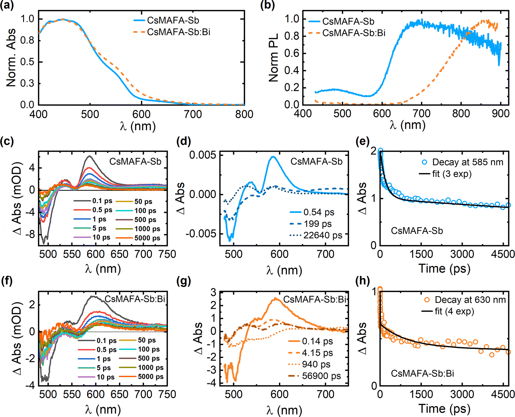 | ||
| Fig. 3 (a) Normalized absorption spectra and (b) steady-state PL spectra of CsMAFA-Sb and CsMAFA-Sb:Bi films. (c and d) TA spectra (raw, chirp-corrected data) of CsMAFA-Sb at different pump-probe delay times, excited at 400 nm. (e) TA decay curve of CsMAFA-Sb monitored at 585 nm. The corresponding tri-exponential decay fit is also shown. (f and g) TA spectra (raw, chirp-corrected data) of CsMAFA-Sb:Bi at different pump-probe delay times, excited at 400 nm. (h) TA decay curve of CsMAFA-Sb:Bi monitored at 585 nm. The corresponding four-exponential decay fit is also shown. | ||
It is known that charge-carrier dynamics in LHP thin films can be studied by probing transitions in the UV-visible and near-infrared regions.49,50 Therefore, time-resolved optical spectroscopy, such as transient absorption spectroscopy or time-correlated single photon counting techniques – provide unique insight into the excited state dynamics of these materials.51–55 For the archetypal MAPbI3 perovskite, charge-carrier lifetimes can be as long as 2 ms after the initial relaxation of “hot” charge carriers to the conduction band edge (∼1 ps).53 Here, we used femtosecond transient absorption spectroscopy (TAS) to monitor the charge-carrier dynamics in our novel PIM materials, having demonstrated in an earlier study that Sb-PIM materials appear to have relatively short charge-carrier lifetimes (nanoseconds) and weak emission.18 Previous knowledge on the nature of similar materials, literature reports, and the shape of steady-state emission bands (broad with large Stokes Shift) suggest the presence of carrier self-trapping, which are typical of PIMs.
Reported charge-carrier mobilities in lead iodide perovskite films are 10–30 cm2 V−1 s−1 for highly crystalline samples of MAPbI3.56 AFM imaging of antimony halide absorber layers reveals a mean crystal size of 100 nm for the reference CsMAFA-Sb material, which is smaller than that usually observed in spin-coated MAPbI3 films (up to microns).34 In the case of MAPbI3, exceptionally long charge-carrier diffusion lengths (∼μm) have been observed,57 but it has been suggested that grain boundaries are not necessarily recombination centers.58 This raises the question of whether grain size is the main concern for recombination compared to bulk defect densities.
CsMAFA-Sb, being the reference material from an earlier study, was revalidated by exciting thin film samples of CsMAFA-Sb (on FTO glass) at 400 nm in transmission geometry. We once again observed a strong bleaching feature centred at 500 nm accompanied by distinct peaks at 530 and 600 nm, and a characteristic Stark shift (Fig. 3c).
For femtosecond TAS measurements, the Sb–Bi containing PIM (CsMAFA-Sb:Bi) exhibits a distinct spectral profile and kinetics compared to CsMAFA-Sb (Fig. 3d–h). It is known that self-trapping may be promoted in bismuth containing PIMs, which can be related to the material's typically lower dimensionality.59 It is important to distinguish between different carrier–phonon interactions in these materials. The so-called Fröhlich interaction is active in polar crystals and in most typical inorganic crystalline semiconductors, allowing for higher charge-carrier mobility associated with large polarons (i.e., in MAPbI3), depending on factors such as the dielectric function and longitudinal optical phonon energies. Coupling to acoustic phonons, on the other hand, when sufficiently strong, can severely reduce charge-carrier mobility and lead to ultrafast charge-carrier localisation, also referred to as self-trapping of charge carriers into small polaron states.
Global fitting of the TA decays for the Sb and Sb–Bi PIM thin-film samples requires different models. CsMAFA-Sb transient absorption data is adequately described by a tri-exponential model, where a sub picosecond component is majorly assigned to ultrafast carrier self-trapping, the ≈100 ps to a non-radiative trap state, and the longer >10 ns decay to weak radiative emission.18 This model does not adequately describe the CsMAFA-Sb:Bi system, where a fourth exponential component becomes necessary to obtain satisfactory fit residuals (Fig. 3h). The additional component corresponds to a broadening of the spectrum (Fig. 3g). Now there is a second “ultrafast component” of <5 ps. Based on the conjecture above regarding the role of bismuth in PIMs, this additional component appears consistent with an additional self-trapped state where there is strong coupling to an acoustic phonon. This may be linked to the increased local lattice distortion in CsMAFA-Sb:Bi compared to CsMAFA-Sb.60 Therefore, the carrier self-trapping process is present in both CsMAFA-Sb and CsMAFA-Sb:Bi, but enhanced in the latter. Note that these findings were independent of excitation wavelength when tested additionally by exciting the samples at 500 nm.
As discussed by Wright et al.61 and Righetto et al.,62 charge carriers in Bi- and Sb-based double halide perovskites undergo, self-trapping within ∼ps of photoexcitation. Such localisation process radically changes the transport regime of the charge carriers in the material: photogenerated free charge carriers which exhibit bandlike transport of large polarons rapidly transfer to a small-polaronic state – associated with strong electron–phonon interactions63 – which diffuse through the material by temperature-activated hopping transport. The poorer electronic coupling and energy barriers associated with the hopping process lead to lower values of charge-carrier mobility. Hence, changes in the charge-carrier mobility over a picosecond timescale – caused by charge-carrier localisation – make optical pump THz probe (OPTP) spectroscopy a powerful technique to reveal the signatures of this process in our materials.
Fig. 4(a)–(d) show the normalised OPTP transients measured for the Sb and Sb–Bi PIM thin films following excitation with a 400 nm pump. The initial effective electron–hole sum mobility (Φμ) in these materials can be extracted from the peak of the photoconductivity signal (see Note 3, ESI, for details†) and ranges from 0.16 cm2 V−1 s−1 for the CsMAFA-Sb thin film to 0.08 cm2 V−1 s−1 for the CsMAFA-Sb:Bi (70:30) thin film. We note here that the extracted mobility value Φμ is an effective mobility, where Φ accounts for the photon-to-free charge-carrier branching ratio (0 < Φ < 1). In materials with low exciton binding energies, such as conventional metal halide perovskites, Φ can be safely assumed to be ∼1,64 and therefore, the Φμ reflects the actual value of μ. However, in materials with higher exciton binding energies, the absorption of high-energy photons yields both excitons and free charge carriers, which coexist in a ratio generally estimated by the Saha equation.65,66 Therefore, the reported effective mobility values Φμ65 for Sb- and Sb–Bi PIMs represent a lower bound of charge-carrier mobility in these materials.
 | ||
| Fig. 4 Normalized photoinduced THz conductivity transients measured for (a) reference CsMAFA-Sb (b) target CsMAFA-Sb:Bi (90:10) (c) CsMAFA-Sb:Bi (80:20) and (d) CsMAFA-Sb:Bi (70:30) thin films after 3.1 eV pulsed excitation. The values for the initial electron–hole sum mobility extracted from the peak of the photoconductivity (based on the methodology described in Note 3, ESI†) are reported on the figures. | ||
Crucially, for all the compositions studied, the OPTP transients show an ultrafast decay of the photoconductivity signal. Such ultrafast decay has been previously observed in a number of Bi-based materials such as Cs2AgBiBr6,61 AgBiS2,62 Cu–Ag–Bi iodides,46 NaBiS267 and Ag–Bi iodides,68 and it has been shown to be a hallmark of charge-carrier localisation. Given that a strong correlation between reduced electronic dimensionality and small polaron formation has been established theoretically and shown experimentally,69–71 we attribute the ultrafast photoconductivity decay to charge-carrier localisation. Further support for the presence of charge-carrier localisation processes in CsMAFA-Sb and CsMAFA-Sb:Bi can be obtained by a comparative analysis of the TAS and OPTP transients. While the main bleaching signal observed in TAS, which is indicative of band-edge population, shows a long-lived decay with a significant signal amplitude (∼50% of the initial amplitude) at 4500 ps, the photoconductivity decays almost completely within ∼2 ps (which well correlates with the ultrafast decay observed in TAS transients). A similar contrast between the TAS and OPTP transients has been reported by Lal et al.68 in Ag–Bi iodides, where the difference in dynamics of TAS and OPTP has been attributed to an ultrafast decay of the mobility caused by the formation of small-polaronic state. Importantly, the observation of highly Stokes-shifted and extremely broad PL spectra in CsMAFA-Sb and CsMAFA-Sb:Bi thin films is in line with the PL reported for materials that show the presence of ultrafast charge-carrier localisation.
We note that the lack of a significant remnant photoconductivity signal after the initial ultrafast localisation suggests that the mobility of the small-polaronic state is below the sensitivity of our technique (∼0.01 cm2 V−1 s−1). Such low mobility values of the localised charge-carrier suggest a remarkably strong charge-carrier localisation with a high energetic barrier governing the site-to-site hopping transport. We note that, in principle, low charge-carrier mobilities do not preclude the possibility of charge-carrier extraction, as the observed charge-carrier dynamics in TAS for both Sb and Sb–Bi PIMs indicate an extremely long charge-carrier lifetime and hence suggests a non-negligible charge-carrier diffusion length.
While the self-trapping in the Sb–Bi PIM samples is enhanced compared to the reference CsMAFA-Sb PIM, the effective mobility of CsMAFA-Sb:Bi is comparable to that of CsMAFA-Sb. On the other hand, CsMAFA-Sb:Bi has larger grain sizes and fewer grain boundaries than CsMAFA-Sb, which may lead to improved charge extraction and reduced charge recombination. Local structural differences between CsMAFA-Sb and CsMAFA-Sb:Bi may also influence their stability trends. To verify our hypotheses, we studied the influence of Bi incorporation into CsMAFA-Sb on its solar cell performance, including operational stability.
2.4. Solar cell performance
To study the effect of cation engineering, i.e., Bi incorporation into CsMAFA-Sb on its solar cell performance, we fabricated planar n–i–p devices using CsMAFA-Sb or CsMAFA-Sb:Bi as light-harvesting layers. The device structure was FTO|c-TiO2|absorber (CsMAFA-Sb or CsMAFA-Sb:Bi)|P3HT|Au, where c-TiO2 and poly(3-hexylthiophene-2,5-diyl) (P3HT) were selected as the electron-transport layer (ETL) and hole-transport layer (HTL), respectively. The details of the solar cell fabrication are provided in the Methods section.
Fig. 5a shows the statistical distributions of the PCE of the CsMAFA-Sb and CsMAFA-Sb:Bi devices, evaluated under 1-Sun illumination (AM 1.5 G, 100 mW cm−2). The distributions of other device parameters fill factor (FF), open-circuit voltage (VOC), and short-circuit current (JSC) are presented in Fig. S19 (ESI).† The PCE of the champion CsMAFA-Sb device is 2.61%, which is slightly higher than the previously reported 2.47% for the same absorber and device configuration.18 On the other hand, the highest PCE of 3.05% among the CsMAFA-Sb:Bi devices is notably higher than that of the reference CsMAFA-Sb devices (Fig. 5a). The current density (J)–voltage (V) curves of the champion CsMAFA-Sb:Bi device are shown in Fig. 5b, which yielded a stabilized PCE of approximately 2.8% under continuous maximum power point (MPP) tracking for 3 min (inset of Fig. 5b). A photocurrent density overestimation of less than 10% between JSCJ–V of 6.6 mA cm−2 (Fig. 5b) and JEQESC of 6.1 mA cm−2 (Fig. 5c) observed in this device suggests that our J–V measurements are reasonably accurate.72 The average PCE values of 2.3–2.4% for the CsMAFA-Sb:Bi devices more accurately represents their realistic performance. On average, most improvements are observed in all device parameters (see Table 1) of the CsMAFA-Sb:Bi devices compared to the CsMAFA-Sb devices. We can expect that the enlarged crystal grains, and consequently the reduced grain boundary count in the CsMAFA-Sb:Bi devices, will mitigate recombination losses and contribute to the VOC gain.73 Fig. S20 (ESI)† shows the statistical distributions of the PCE for four types of devices: CsMAFA-Sb, CsMAFA-Sb with DMSO, CsMAFA-Sb:Bi with DMSO, and CsMAFA-Sb:Bi. The average and champion PCE values of the CsMAFA-Sb:Bi, DMSO devices are slightly higher than that of the CsMAFA-Sb, DMSO devices. This is despite both having photoactive layers processed with an 80:20 solvent ratio of DMF and DMSO and similar morphological features (see Fig. S10 and Table S4, ESI†). This suggests that the increase in PCE for the Sb–Bi alloyed devices is due to both the larger crystal size from solvent engineering and the incorporation of bismuth.
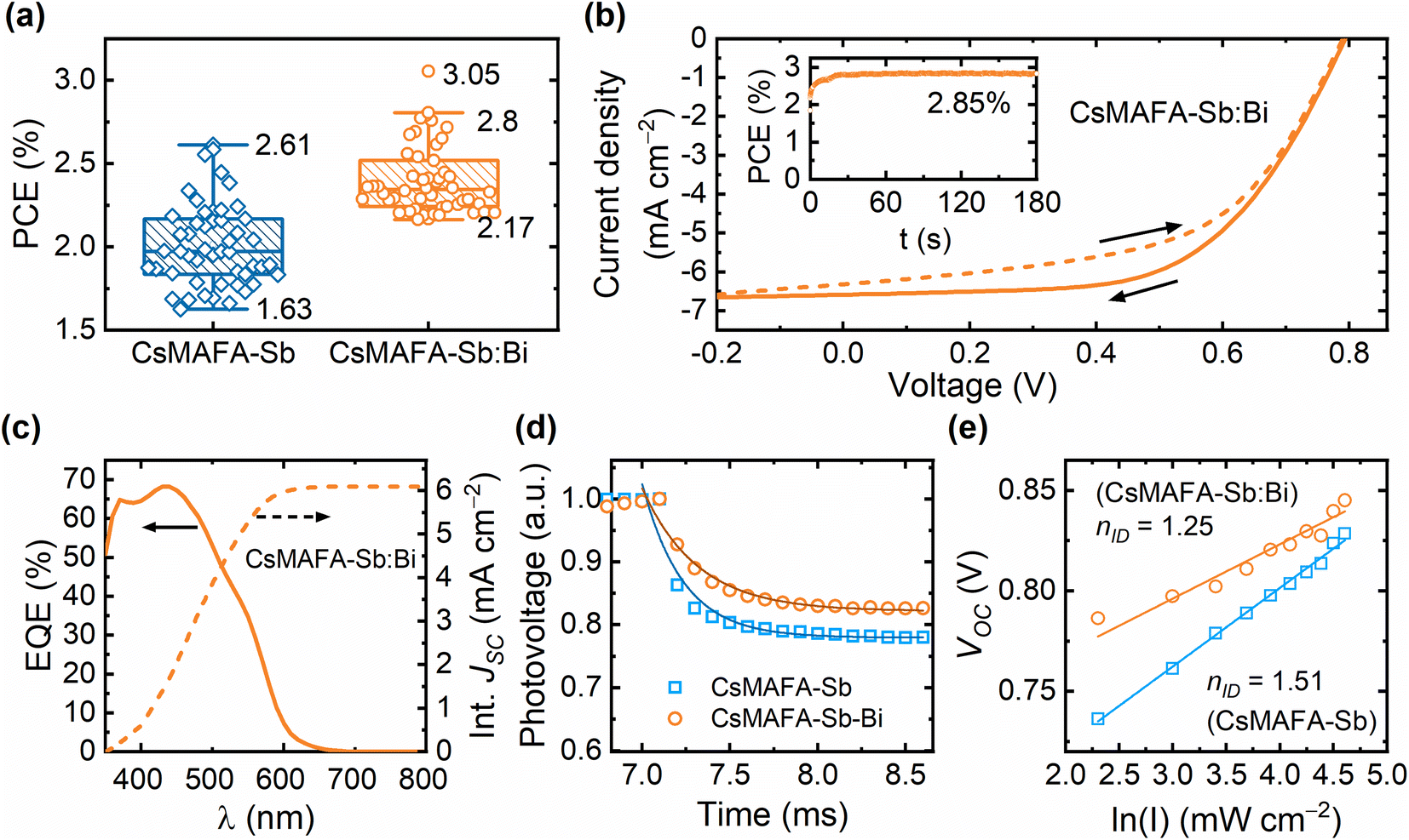 | ||
| Fig. 5 (a) Statistical distribution (over 50 devices) of the power conversion efficiency of CsMAFA-Sb and CsMAFA-Sb:Bi devices under 1-Sun illumination. (b) J–V curves of the champion CsMAFA-Sb:Bi device under 1-Sun illumination. The arrows indicate the scan direction. The stable power output (SPO) behaviour of the devices near the MPP under continuous 1-Sun illumination intensity is shown in the inset. (c) EQE spectrum and the integrated JEQESC profile of the CsMAFA-Sb:Bi device. (d) TPV decay curves of CsMAFA-Sb and CsMAFA-Sb:Bi. (e) Variations of VOC and with increasing light intensity (0.1–1.1 Sun) for the CsMAFA-Sb and CsMAFA-Sb:Bi devices. | ||
| Absorber | PCE (%) | FF (%) | J SC (mA cm−2) | V OC (V) |
|---|---|---|---|---|
| CsMAFA-Sb | 2.01 ± 0.25 | 45.9 ± 7.6 | 6.19 ± 1.08 | 0.73 ± 0.03 |
| CsMAFA-Sb:Bi | 2.40 ± 0.21 | 49.3 ± 5.8 | 6.53 ± 0.77 | 0.75 ± 0.03 |
We conducted electrochemical impedance spectroscopy (EIS) measurements on both CsMAFA-Sb and CsMAFA-Sb:Bi devices to investigate the effect of compositional engineering on the charge transport and recombination kinetics of these devices. Fig. S21 (ESI)† shows the complex Nyquist plots that exhibits two distinct behaviours merging with each other: a high-frequency (HF) process and a low-frequency (LF) process. The HF part corresponds to electronic charge transport and bulk recombination, while the LF part is related to ionic kinetics and interfacial recombinations.74,75 The Nyquist spectra were fitted using two distinctly separated Randle circuits (RHF/CHF and RLF/CLF) as shown in Fig. S22 and S23 (ESI),† suggesting that two distinct processes with different time constants have converged into a single depressed semicircle in the Nyquist spectra. In electrical equivalent circuit (EEC), Rs represents the series resistance, while RHF and RLF denote the high-frequency and low-frequency resistances, respectively. In perovskite solar cells, the total recombination resistance (Rrec = RHF + RLF) is typically the sum of high- and low-frequency resistances. However, it also includes a contribution from the resistance of the selective contacts; therefore, this is valid only for a comparative study.76 All device resistance parameters for each composition are provided in Fig. S24 (ESI).† It can be noted that the total recombination resistance of devices of CsMAFA-Sb:Bi compositions is significantly higher compared to the reference Sb-only containing devices, resulting in a lower Shockley–Read–Hall (SRH) recombination rate in the former case. This phenomenon could be attributed to a reduction in carrier trapping both in the bulk and at the interfaces of CsMAFA-Sb:Bi, linked to the reduced number of grain boundaries. The light-intensity dependence of VOC and JSC of the devices further supports this observation. The CsMAFA-Sb:Bi device has a lower ideality factor ((nID), 1.25 vs. 1.51) and a higher exponent value (0.97 vs. 0.93) compared to the CsMAFA-Sb device (see Fig. 5e and S25, ESI†), indicating reduced trap-assisted recombination.
2.5. Operational stability and ion migration dynamics
To assess the real-world operational stability of the two types of PIM solar cells, we conducted MPP tracking measurements following International Summit on Organic Photovoltaic Stability (ISOS) protocols.5 We first evaluated the long-term stability of CsMAFA-Sb and CsMAFA-Sb:Bi devices under 1-Sun illumination (ISOS-L1), as shown in Fig. 6a. A continuous N2 gas flow was applied to eliminate the influence of external stresses such as moisture and oxygen. While the thin film samples of CsMAFA-Sb and CsMAFA-Sb:Bi remain largely unchanged under sunlight soaking (with no applied voltage bias) for 100 hours, as evidenced by the unchanged absorption spectra (Fig. S26, ESI†) and XRD patterns (Fig. S27, ESI†), the corresponding devices experienced a rapid initial efficiency drop (Fig. 6a), often referred to as ‘burn-in’. However, the CsMAFA-Sb:Bi device demonstrated a T80 value of 17 hours, which is twice that of the 8.2 hours of the CsMAFA-Sb device (Table 2). This performance of CsMAFA-Sb:Bi is significantly higher compared to the limited operational stability studies on pnictogen-based halide PIMs, where T80 values are typically less than a couple of hours.15–17 After the initial ‘burn-in’ period, the CsMAFA-Sb device continued to lose performance over 100 hours, with its residual efficiency dropping to 45% (see Fig. 6a and Table 2). This efficiency degradation can be attributed to ion migration under light and voltage bias, which causes mobile ion-field screening.4,77,78 The higher hysteresis index values (Fig. 6b) at different scan rates (see Fig. S28, ESI†) observed for the CsMAFA-Sb devices compared to the CsMAFA-Sb:Bi devices indicate a high accumulation of mobile ions at the PIM-charge transport layer interfaces. This results in built-in electric field screening, reducing charge extraction efficiency.78 This contributes to the rapid performance degradation of the CsMAFA-Sb device under continuous operation. | ||
Fig. 6 Aging studies of unencapsulated CsMAFA-Sb and CsMAFA-Sb:Bi solar cells in a N2 atmosphere. (a) MPP tracking of both devices under 1-Sun illumination at room temperature (RT ≈ 28 °C). The initial PCEs of the CsMAFA-Sb and CsMAFA-Sb:Bi devices are 2.5% and 2.2%, respectively. (b) Distribution of hysteresis index of both the devices. Hysteresis index = (PCEREV/PCEFOR) × 100%–100%. (c) Imaginary impedance as a function of frequency. (d) Magnitude of impedance as a function of frequency for both devices. Transient dark current curves of (e) CsMAFA-Sb and (f) CsMAFA-Sb:Bi devices. Two regions of voltage application of 0.4 V and 0 V are shown. The ionic charge was estimated using: 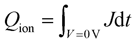 . (g) The I–Sb(Bi)–I angles in the pnictogen halide octahedra from the crystal structures of CsMAFA-Sb and CsMAFA-Sb:Bi, which were determined using Rietveld refinement of the corresponding XRD patterns. . (g) The I–Sb(Bi)–I angles in the pnictogen halide octahedra from the crystal structures of CsMAFA-Sb and CsMAFA-Sb:Bi, which were determined using Rietveld refinement of the corresponding XRD patterns. | ||
| Device | T 80 (h) | PCE0 (%) |
|---|---|---|
| CsMAFA-Sb | 8.2 | 45 |
| CsMAFA-Sb:Bi | 17 | 73 |
On the other hand, the CsMAFA-Sb:Bi device exhibited a decreased efficiency loss, achieving a residual efficiency of 73% (Fig. 6a and Table 2). In the imaginary impedance-frequency spectra (Fig. 6c), the low-frequency (LF) response exhibits a characteristic lifetime (τLF) increase from 5.6 ms in CsMAFA-Sb device to 11.37 ms in CsMAFA-Sb:Bi, indicating that ion diffusion/migration in these Sb–Bi PIM-based devices is considerably slower than in the pure Sb-based devices.79 This, in turn, can result in a higher activation energy requirement for ion migration in CsMAFA-Sb:Bi devices compared to CsMAFA-Sb devices.79 Additionally, the Sb–Bi-based PSCs display significantly higher real part of impedance at low frequencies (Fig. 6c and d) and exhibit a longer recombination time constant (3.18 × 10⁻⁴ s vs. 1.16 × 10⁻⁴ s for CsMAFA-Sb) in transient photovoltage (TPV) measurements (Fig. 5d). This provides further evidence that the presence of ionic defects has been suppressed in the CsMAFA-Sb:Bi devices. Furthermore, we calculated the ionic charges in the devices using dark transient current measurements (Fig. 6e and f). Initially, a pre-bias of 0.4 V was applied in the dark to bring the devices into equilibrium. The external bias was then instantly removed, and the resulting dark current transient was recorded as the devices re-equilibrated at 0 V. Since no electronic injection occurs during this process, the ionic charge was determined by integrating the ionic current over the re-equilibration period. The approximate ionic charges in Sb and Sb–Bi PIM devices are 1.0 × 10⁻⁶ C cm−2 and 5.38 × 10⁻⁷ C cm−2, respectively.
Our structural calculations show that adding Bi ions to the SbI6 lattice increases the distortion index, M–I (M = Sb, Bi) bond length, and M–M bond distance (see Fig. 6g and Table S9, ESI†). The larger bond distance and higher distortion index create more lattice strain, which alters the migration paths of iodine ions and raises the energy barrier for their movement. Consequently, the distorted lattice restricts ion movement, particularly iodine, making it harder for these ions to migrate within the structure. This increased lattice strain due to Bi incorporation is linked to the improved operational stability of the CsMAFA-Sb:Bi devices.
We also calculated the bond angle variance, which is the average of the squared differences between the observed bond angles and the ideal bond angles, based on the experimentally observed bond lengths for both CsMAFA-Sb:Bi and CsMAFA-Sb using the following formula.

The higher bond angle variance of 30.4935 degree2 for CsMAFA-Sb:Bi compared to 12.4032 degree2 for CsMAFA-Sb indicates significantly greater local structural distortions. The higher bond angle variance, leading to increased local disorder, may introduce additional trap states in CsMAFA-Sb:Bi due to poor orbital overlap and inconsistent bonding environments. Nevertheless, the presence of Bi strengthens the local bonding network by introducing stronger Sb/Bi–I/Cl bonds. This effectively suppresses ionic migration by restricting the movement of mobile ions within the lattice, contributing to improved compositional stability of CsMAFA-Sb:Bi under operational stress. Additionally, Bi, with its larger ionic radius and stronger covalent bonding with iodine and chlorine, helps stabilize the local coordination environment. This may reduce the probability of forming under-coordinated sites and vacancy-related defects, contributing to reduced non-radiative recombination pathways in devices employing CsMAFA-Sb:Bi.
Furthermore, both the CsMAFA-Sb and CsMAFA-Sb:Bi devices showed improved stability trends under low-light 0.1-Sun intensity (Fig. S29, ESI†). This is because the activation energy of ion migration typically decreases with lowering of light intensity, thereby increasing the barrier for ion migration.21,80 The stable and improved performance (4% PCE under 0.1-Sun) of the CsMAFA-Sb:Bi device under low-light intensities suggests it could be a promising candidate for indoor PV applications.
Assessing the thermal stability of solar cells provides valuable information for their potential commercial viability. Solar cells must endure elevated temperature (e.g., 65 °C and 85 °C) to meet the key metrics set by ISOS for assessing their tolerance to operational temperatures and for accelerated degradation testing.5,81 We, thus, performed aging tests by conducting MPP tracking for the CsMAFA-Sb:Bi devices at elevated temperatures of 65 °C and 85 °C (ISOS-L2). Fig. S30a (ESI)† shows the comparison of MPP trends at room temperature and 65 °C. The initial burn-in process speeds up at 65 °C, significantly reducing the initial T80 from 8 hours to just 0.3 hours as the temperature rises from room temperature (Fig. S30b, ESI†). This accelerated efficiency loss is typically due to the increased ion migration at higher temperatures.82 However, after the initial rapid decay, the efficiency gradually recovered and eventually stabilized, achieving a residual PCE of 84% after 100 hours, which is higher than the 73% residual PCE of the device aged at room temperature during the same duration. Even at 85 °C, the recovery process was present, which partially mitigated the initial rapid performance decline (Fig. 7a). Notably, the device maintained a residual PCE of 84% after 215 hours of MPP tracking at 85 °C. The projected T80 is 275 hours, which is significantly higher than that observed at room temperature (Table 2). This T80 value of CsMAFA-Sb:Bi device at 85 °C surpasses that of comparable n–i–p organic–inorganic LHP state-of-the-art device structures with P3HT as the HTL (Table S10, ESI†) and TiO2 as the ETL. In fact, the T80 of our cells (275 hours) is even higher than that of recently reported hybrid LHP devices using a new-generation of thiophene-based polymeric HTLs. These devices showed T80 values of 100 hours at a high temperature of 65 °C (200 hours with dopants in the polymeric HTL).81
 | ||
| Fig. 7 (a) MPP tracking of a CsMAFA-Sb:Bi (unencapsulated) device (2.4% initial PCE) under 1-Sun illumination at 85 °C under N2 atmosphere. The T80 value was predicted by extrapolating the experimental data.83 The J–V curves of the device are shown (b) before and (c) after the tracking. | ||
The initial drop and subsequent recovery in the PCE under MPP tracking and illumination were also observed for LHP devices using polymeric HTLs, including P3HT. However, we noticed the efficiency recovery for the CsMAFA-Sb:Bi devices only under MPP tracking at high temperatures (Fig. 7a and S30, ESI†). The recovery phenomenon was attributed to the neutralization of photogenerated small polarons in the absorber layer by delocalized polarons in the polymeric HTL through an interfacial interaction. Furthermore, the high-temperature MPP efficiency trends (Fig. 7a and S30, ESI†) almost mirror the corresponding photocurrent trends (Fig. S31, ESI†). The initial rapid decay in the MPP current reduces charge extraction efficiency and thereby the photocurrent due to mobile ion-field screening (Fig. S30, ESI†). We speculate that the subsequent recovery of the MPP current, JMPP, under the high temperatures (Fig. S31, ESI†) was caused by a disruption in the ion-field screening due to changes at the interface, leading to the observed MPP trends (Fig. 7a and S30, ESI†). The reduced hysteresis between the J–V curves (measured at room temperature) after MPP tracking at 85 °C (see Fig. 7b, c and Table S11, ESI†) may also suggest the reduced ion-field screening in the aged device.
We inspected the CsMAFA-Sb:Bi device aged at 85 °C after it completely cooled down to room temperature (refer to Fig. S32 and Note 4, ESI†). The SEM images (Fig. S32b and c, ESI†) of the PIM layer in the aged device show a fused morphology, which is significantly different from the regular morphology of CsMAFA-Sb:Bi with clearly defined grain boundaries (refer to Fig. 2b and S32d, ESI†). The VOC gain of 25–65 mV in the aged device may be attributable to the reduced number of grain boundaries and mobile ions at the interfaces. However, it is not yet clear whether the efficiency recovery process at 85 °C (Fig. 7a) is solely related to the morphology change. Future studies focusing on the in situ monitoring of the evolution of structural and morphological characteristics of the Sb-PIM layer (and other device layers as well) under operational conditions (light, voltage bias, and heat) may shed light on the exact mechanism behind the efficiency recovery process observed under high-temperature MPP tracking of CsMAFA-Sb:Bi devices (Fig. 7 and S32, ESI†).
3. Conclusions
Our study investigates the accelerated aging of pnictogen-based halide PIM solar cells and unveils the correlation between local structural changes and their stability during continuous operation. The Sb–Bi co-alloying in the triple A-site cation Sb-PIM, CsMAFA-Sb, resulting in CsMAFA-Sb:Bi, has a profound impact on the structural, optical, and solar cell properties of this absorber. Pnictogen co-alloying leads to reduced local structural symmetry, slightly increased carrier self-trapping, improved film morphology, and enhanced solar cell performance. Additionally, CsMAFA-Sb:Bi devices exhibit significantly lower performance losses under MPP tracking with 1-Sun illumination compared to CsMAFA-Sb devices. We attribute the reduced ion migration in the Sb–Bi mixed PIM devices, which is responsible for the enhanced stability, primarily to the enhanced local crystal distortion. The CsMAFA-Sb:Bi devices demonstrate impressive operational stability at a high temperature of 85 °C, maintaining more than 80% of the initial PCE even after 200 hours of accelerated aging tests. This performance is comparable or even surpasses that of the best-performing LHP solar cells employing similar charge-transport layers (TiO2 as ETL and P3HT or new-generation thiophene-based polymers as HTLs). The performance and operational lifetime of CsMAFA-Sb:Bi solar cells can be further improved by adopting strategies such as interfacial engineering, bulk passivation, and charge transport layer screening.While LHPs currently offer superior solar cell PCE and operational stability, making them highly suitable for rooftop and utility-scale applications, they become non-ROHS compliant for indoor photovoltaic applications due to high Pb content (especially on flexible substrates) and toxic exposure risks. Although the current study primarily focuses on the improved device stability of PIM devices under 1-Sun, these enhancements are also crucial for their indoor photovoltaic applications with theoretical PCEs of 50%. Furthermore, wide bandgaps of PIMs make them suitable for tandem solar cells, a highly researched area due to high efficiency from tunable bandgaps of LHPs. However, mixed halide LHPs required for these wide bandgaps face stability issues due to halide segregation. Therefore, our efforts to improve their operational stability lay a foundation for future advancements in both efficiency and stability for a wide range of photovoltaic applications of PIMs.
Previous studies have shown that pnictogen mixing improves the performance of PIMs in solar cells through structural and morphological enhancements. Our findings reveal, for the first time, that pnictogen mixing is also an effective approach to enhance the stability of PIM-based devices under operational conditions, including thermal stress, by establishing a structure-operational stability relationship. Overall, the field of pnictogen-based halide PIMs is still in its early stages with significant room for improvement. Nevertheless, our results unequivocally highlight the promise of this material family as one of the most interesting emerging absorbers, particularly when environmental impact, air stability, and operational stability are prioritized.
4. Methods
4.1. Materials
Antimony iodide (SbI3, 99.999%) was purchased from Fisher. Cesium iodide (CsI, 99.999%) was purchased from ABCR. Methylammonium chloride (MACl, 99.99%) and formamidium iodide (FAI, 99.99%) were purchased from Greatcell Solar Materials. Dimethyl sulfoxide (DMSO, anhydrous, ≥99.9%), N,N-dimethylformamide (DMF, anhydrous, ≥99.8%), chlorobenzene (anhydrous, 99.8%), fuming (>37%) hydrochloric acid (HCl), titanium diisopropoxide bis(acetylacetonate) 75 wt% in 2-propanol, and 2-propanol (anhydrous 99.5%) were purchased from Sigma-Aldrich. Titanium(IV) isopropoxide (TTIP) (99 wt%), acetylacetone was purchased from Acros Organics. Ethanol (96.6 vol%) was received from Estonian Spirit. Poly(3-hexylthiophene-2,5-diyl) (P3HT, electronic grade, regioregular) was purchased from Rieke Metals. All the chemicals were used as received, without any further purification.4.2. Solution preparation
The CsMAFA-Sb PIM was fabricated according to Lamminen et al.18 The CsMAFA-Sb:Bi precursor was prepared by mixing 90 vol% Sb and 10 vol% Bi-containing precursors together. The Sb containing precursor was the same as in CsMAFA-Sb (SbI3, CsI, MACl and FAI in the molar ratio 1.0:1.2:1.5:0.3, with 150 mol% of MACl and 30 mol% of FAI compared to the amount of SbI3, at a concentration of 444 mg ml−1) except the solvent was a 1:1 mixture of DMF and DMSO instead of the fully DMF solvent used in CsMAFA-Sb. For 1000 μl of the Sb precursor solution the amounts were SbI3 230.47 mg, CsI 143.0 mg, MACl 46.45 mg, FAI 23.66 mg, DMF 500 μl, and DMSO 500 μl. The Bi precursor contained BiI3, CsI, MACl and FAI in the molar ratio 1.0:1.2:1.5:0.3, with 150 mol% of MACl and 30 mol% of FAI compared to the amount of BiI3 in 1:1 DMF and DMSO solution. The concentration of the Bi containing precursor was 484 mg ml−1. For 500 μl of the Bi precursor solution the amounts were BiI3 135.25 mg, CsI 71.5 mg, MACl 23.25 mg, FAI 12 mg, DMF 250 μl, and DMSO 250 μl. The precursors were kept under magnetic stirring for at least 4 hours before use to dissolve all powders completely. To make 1000 μl of the CsMAFA-Sb:Bi precursor 900 μl of the Sb precursor and 100 μl of the Bi precursor were mixed.
The precursors with different DMF to DMSO concentrations (80% DMF and 20% DMSO) where fabricated as described above, with the only difference being the ratios of DMF and DMSO.
4.3. Solar cell fabrication
The solar cells were fabricated onto FTO coated substrates (TEC15 2.2 mm thick from Greatcell Solar Materials or 2.2 mm thick from Sigma-Aldrich), which were cut into 2 × 2 cm pieces and patterned by etching. The FTO was protected with tape (Scotch Magic tape) on the area that was not etched. The area to be etched was covered with a thin layer of zinc powder and the substrate was submerged in 2 M hydrochloric acid solution for 5 minutes. The zinc was removed after the 5-minute reaction time by brushing while the substrate was still in the solution. After etching the tape was removed and the substrates were cleaned with water. The substrates were cleaned by brushing with soap (2% Mucasol), rinsing with ultra-pure water and 15-minute consecutive sonication in ultra-pure water, acetone and 2-propanol and dried with N2 flow.Two different methods were employed for the fabrication of a compact titanium dioxide (TiO2) layer. In the first method, the TiO2 layer was fabricated onto the etched and cleaned substrates via spray pyrolysis. The precursor was made by diluting titanium diisopropoxide bis(acetylacetonate) 75 wt% in 2-propanol with 2-propanol. The typical amounts were 1.15 ml of titanium diisopropoxide bis(acetylacetonate) 75 wt% and 4.95 ml 2-propanol. The precursor was deposited on the substrates by spraying 13 short cycles with 20 s between the cycles onto the substrates on a hotplate at 450 °C. After the final spray cycle the substrates were annealed for 45 minutes at 450 °C. In the second method, the TiO2 thin films were deposited from solution containing titanium(IV) isopropoxide and acetylacetone in a molar ratio of 1:1 in ethanol. The films were deposited by ultrasonic spray pyrolysis at substrate temperature of 340 °C, applying 70 spray cycles. The as-deposited TiO2 films were then annealed at 450 °C for 30 min in air. The thickness of the TiO2 thin film is ca. 30 nm. No marked difference was noted in the efficiency of the solar cells when comparing the two different TiO2 deposition methods. The substrates were stored in closed containers in darkness before use. Immediately before the PIM deposition, the substrates were treated with 5 minutes of UV-ozone.
The PIM layers were deposited by spin-coating inside a N2 glove box. Before starting the spin-coating program (3000 rpm for 30 s, acceleration within 5 s) 40 μl of the precursor was pipetted onto the TiO2 coated substrate. During the spin-coating 150 μl of antisolvent, 2-propanol, was added onto the rotating substrate. The timing of 2-propanol addition depended on the DMSO ratio of the precursor. For CsMAFA-Sb where the precursor was fully DMF this was right before the point when the film starts to change colour. For the precursors with 20% DMSO the antisolvent was added 20 seconds before the end of the spin coating program. For the precursors where there was 50% DMSO the antisolvent was added 10 seconds before the end of the spin coating program. The antisolvent delay with the 50% DMSO containing films was to produce smooth films. After spin-coating the substrates were annealed on a hotplate at 130 °C for 10 min.
P3HT was used as the hole transport material. 80 μl of the solution (20 mg ml−1 in chlorobenzene) was spin-coated dynamically in the N2-filled glove box. The spin-coating program was 2000 rpm for 30 s. The method was adapted from literature.84 After spin coating the HTM, the substrates were annealed at 80 °C on a hotplate for 10 min. The solar cell was completed by thermally evaporating a 100 nm thick gold contact under a 6 × 10⁻⁶ mbar vacuum. Each substrate held 3 solar cells with an active area of 20 mm2 each.
4.4. X-ray diffraction (XRD)
XRD patterns of the PIM films were collected using Cu Kα radiation on an Empyrean Alpha 1 high-resolution X-ray diffractometer from Malvern Panalytical. Rietveld refinement of the XRD patterns was performed using GSAS software.4.5. Scanning electron microscopy (SEM)
The scanning electron microscopy (SEM) images of the PIM films on FTO and compact TiO2 were taken using a field emission scanning electron microscope Zeiss Ultra Plus. The operation was at 3 kV.4.6. Atomic force microscopy (AFM)
AFM measurements were performed in conjunction with Kelvin probe force microscopy (KPFM) using a Bruker Dimension Icon microscopy platform under ambient atmospheric conditions. Measurements were performed in triplicate on separate days with different batches.Sequential surface topography and surface potential measurements were performed using the proprietary “PeakForce tapping” KPFM technique. Upon contact with the sample surface, the instrument was allowed to automatically adjust feedback gain and setpoint. Scan lift height was generally between 140 and 150 nm. Under our experimental conditions no electrical bias was applied to the sample. The scan tip used was a Bruker SCM-PIT-V2. Samples were imaged across an area of 5 mm2 and a scan speed of 0.5–1 Hz was used.
CsMAFA-Sb and CsMAFA-Sb:Bi thin films were prepared in two ways: either with the perovskite directly spin coated (vide infra) onto FTO glass or upon a c-TiO2 layer on FTO to better mimic a solar cell device architecture. In either case a 3 mm section of the FTO substrate was left uncoated to facilitate grounding the sample to the microscope chuck. Samples were stored in a glove box under a nitrogen atmosphere before measurements.
For photo-assisted KPFM measurements, external irradiation was provided by a CoolLed pE-4000 light source coupled via a fiber optic connection to a proprietary back illumination assembly. The sample illumination setup is such that it was possible to irradiate the samples with 525 nm light (with a power density of 1 mW cm−2 at the sample) from underneath the sample stage. It can be assumed that the irradiation area is larger than the microscopy sample scan area given the diameter of the optical fibre is 400 mm. The sample stage was calibrated to centre the light on the imaging area. As a practical note we observed that our samples would not be conducive to KPFM surface potential measurements unless there was a c-TiO2 layer underneath the perovskite. Without the compact layer, no distinct features could be identified in the surface potential mapping, and there was a characteristic surface potential decay indicative of surface charging (Fig. S33 and S34, ESI†). The imaging of the samples took approximately 30 minutes to acquire. It is noteworthy that during imaging under 525 nm irradiation there is a trend of the surface potential decreasing over time. The samples' topography did not change after irradiation under our conditions, so this is not necessarily due to decomposition of the perovskite. Instead, it may be an indication of charge saturation under prolonged irradiation.85
Images were processed for the purposes of flattening and removing visual artifacts using the freely available Gwyddion SPM data visualisation and analysis tool (version 2.64).
4.7. Transient absorption (TA) measurements
PIM thin film materials on FTO glass slides underwent pump–probe spectroscopy measurements in transmission mode. The instrumental setup has been described elsewhere.59 Here 100 fs pulses of 800 nm, at rate of 1 kHz were generated by a Libra F laser system (Coherent Inc.) and pump a Topas C OPA (Light Conversion Ltd) to produce excitation pulses at 400 nm or 500 nm. The sample was excited at a rate of 500 Hz through an optical chopper. The excitation power density was set such that photoinduced degradation was minimized during the timespan of data collection (≈100 mW). The pump light was used to produce a white-light continuum probe beam by illuminating a water-filled cuvette. Transient absorption data was collected by an ExiPro, CDP Inc. spectrometer across the UV-visible wavelength range. The practical temporal resolution of the instrument is restricted by the laser delay line and laser pulse width such that spectra are obtained from approx. 0.2 ps to 6 ns. Steady-state emission measurements were obtained with an Edinburgh Instruments FLS-1000 spectrophotometer with samples mounted on an adjustable stage at a shallow angle relative to the excitation beam (monochromatic light from a Xe arc lamp).4.8. Optical pump THz probe spectroscopy
The output from an amplified 800 nm Ti; sapphire laser system (Spectra Physics Mai tai-Ascend-Spitfire) with a 5 kHz repetition rate generating 35 fs pulses is split into three parts. One part is frequency doubled to 400 nm and used to excite the thin film samples and forms the pump beam. The second part is used for THz pulse generation with a spintronic emitter (2 nm tungsten, 1.8 nm Co40Fe40B20, 2 nm platinum on quartz substrate). The gate pulse makes up the last part of the initially split output from the amplified Ti:sapphire laser system. The THz setup is used in transmission mode where the strength of the transmitted THz is detected using electro-optic sampling: the transmitted THz beam is overlapped with the gate beam in a non-linear ZnTe crystal and the change in polarization of the gate beam (proportional to the strength of transmitted THz beam) is detected using a quarter wave plate, polarizing prism and balanced photodiodes. The time delay between the THz and pump pulses is controlled using optical delay stages.
4.9. J–V measurements
The J–V characteristics of the solar cells in 1-Sun AM 1.5G conditions were measured under a Wavelabs SINUS-70 solar simulator in ambient environment. The measurements were conducted with a Keithley 2450 source-monitor unit using a 4-wire setup and using a scan speed of 50 mV s−1. Several batches of solar cells were fabricated and measured to estimate the statistical distribution of the PV parameters. The external quantum efficiency was measured in the dark using the QuantX-300 from Newport. The integrated JSC values were estimated by integrating the EQE spectra over the incident photon flux spectrum of AM 1.5 G spectrum. The maximum power point tracking of the devices under sunlight illumination and/or heat (65 and 85 °C) was conducted using the same solar simulator with the Litos Lite parallel JV system from Fluxim in a N2 atmosphere.4.10. Electrochemical impedance spectroscopy (EIS)
The EIS measurements were carried out by an Ivium Electrochemical Workstation at 0.4 V applied bias in the dark. In EIS, an AC amplitude of 20 mV was applied, and the frequency range was varied from 0.3 MHz to 0.5 Hz to measure the impedance of PSCs. The EIS spectra were analysed using two types of representations: Nyquist plots and Bode plots.74,86 The EIS data has been fitted with Zview software. To assess the recombination time constant of PSCs, we conducted transient photovoltage measurements using a homemade setup with a white light source with an intensity of 1-Sun. The transient photovoltage spectra were fitted by a mono-exponential decay function.Data availability
The data supporting the article have been included as part of the ESI.†Conflicts of interest
There are no conflicts to declare.Acknowledgements
N. L. thanks The Emil Aaltonen Foundation for funding. J. K. thanks Tampere University and Tampere Institute for Advanced Study for funding. S. L. acknowledges funding from the Oxford India Centre for Sustainable Development. M. R. and L. M. H. acknowledge support by the Engineering and Physical Sciences Research Council (EPSRC), UK (EP/V010840/1, EP/Y014952/1, EP/X038777/1). L. M. H. acknowledges support through a Hans Fischer Senior Fellowship from the Technical University of Munich’s Institute for Advanced Study, funded by the German Excellence Initiative. A. K. and I. O. A. acknowledge for funding Estonian Research Council project PRG627, Estonian Centre of Excellence project TK210; TK210U8 and EU Horizon 2020 project 952509-5GSOLAR. R. K. acknowledge Olle Engkvists Stiftelse for postdoctoral research grant. P. V. thanks Research Council of Finland, Decision No. 347772. The work is part of the Research Council of Finland Flagship Programme, Photonics Research and Innovation (PREIN), decision number 346511. The computing resources and the related technical support used for this work have been provided by CRESCO/ENEA-GRID High Performance Computing infrastructure and its staff. CRESCO/ENEAGRID High Performance Computing infrastructure is funded by ENEA, Italy, the Italian National Agency for New Technologies, Energy and Sustainable Economic Development and by Italian and European research programs; see https://www.cresco.enea.it for information. This work made use of Tampere Microscopy Centre facilities at Tampere University.References
- O. Almora, C. I. Cabrera, S. Erten-Ela, K. Forberich, K. Fukuda, F. Guo, J. Hauch, A. W. Y. Ho-Baillie, T. J. Jacobsson, R. A. J. Janssen, T. Kirchartz, M. A. Loi, X. Mathew, D. B. Mitzi, M. K. Nazeeruddin, U. W. Paetzold, B. P. Rand, U. Rau, T. Someya, E. Unger, L. Vaillant-Roca and C. J. Brabec, Adv. Energy Mater., 2024, 14, 2303173 CAS.
- M. A. Green, E. D. Dunlop, M. Yoshita, N. Kopidakis, K. Bothe, G. Siefer, D. Hinken, M. Rauer, J. Hohl-Ebinger and X. Hao, Prog. Photovoltaics Res. Appl., 2024, 32, 425–441 CrossRef.
- Y. Wang, S. R. Kavanagh, I. Burgués-Ceballos, A. Walsh, D. O. Scanlon and G. Konstantatos, Nat. Protoc., 2022, 16, 235–241 CAS.
- H. Zhu, S. Teale, M. N. Lintangpradipto, S. Mahesh, B. Chen, M. D. McGehee, E. H. Sargent and O. M. Bakr, Nat. Rev. Mater., 2023, 8, 569–586 CrossRef.
- M. V. Khenkin, E. A. Katz, A. Abate, G. Bardizza, J. J. Berry, C. Brabec, F. Brunetti, V. Bulović, Q. Burlingame, A. Di Carlo, R. Cheacharoen, Y.-B. Cheng, A. Colsmann, S. Cros, K. Domanski, M. Dusza, C. J. Fell, S. R. Forrest, Y. Galagan, D. Di Girolamo, M. Grätzel, A. Hagfeldt, E. von Hauff, H. Hoppe, J. Kettle, H. Köbler, M. S. Leite, S. (Frank) Liu, Y.-L. Loo, J. M. Luther, C.-Q. Ma, M. Madsen, M. Manceau, M. Matheron, M. McGehee, R. Meitzner, M. K. Nazeeruddin, A. F. Nogueira, Ç. Odabaşı, A. Osherov, N.-G. Park, M. O. Reese, F. De Rossi, M. Saliba, U. S. Schubert, H. J. Snaith, S. D. Stranks, W. Tress, P. A. Troshin, V. Turkovic, S. Veenstra, I. Visoly-Fisher, A. Walsh, T. Watson, H. Xie, R. Yıldırım, S. M. Zakeeruddin, K. Zhu and M. Lira-Cantu, Nat. Energy, 2020, 5, 35–49 CrossRef.
- Q. C. Burlingame, Y.-L. Loo and E. A. Katz, Nat. Energy, 2023, 8, 1300–1302 CrossRef CAS.
- J. Li, H.-L. Cao, W.-B. Jiao, Q. Wang, M. Wei, I. Cantone, J. Lü and A. Abate, Nat. Commun., 2020, 11, 310 CrossRef CAS PubMed.
- C. Ponti, G. Nasti, D. D. Girolamo, I. Cantone, F. A. Alharthi and A. Abate, Trends Ecol. Evol., 2022, 37, 281–283 CrossRef CAS PubMed.
- G. K. Grandhi, D. Hardy, M. Krishnaiah, B. Vargas, B. Al-Anesi, M. P. Suryawanshi, D. Solis-Ibarra, F. Gao, R. L. Z. Hoye and P. Vivo, Adv. Funct. Mater., 2024, 34, 2307441 CrossRef CAS.
- Y.-T. Huang, S. R. Kavanagh, D. O. Scanlon, A. Walsh and R. L. Z. Hoye, Nanotechnology, 2021, 32, 132004 CrossRef CAS PubMed.
- B. Cucco, L. Pedesseau, C. Katan, J. Even, M. Kepenekian and G. Volonakis, Sol. RRL, 2022, 6, 2200718 CAS.
- W. J. Jang, H. W. Jang and S. Y. Kim, Small Methods, 2024, 8, 2300207 CAS.
- H. C. Sansom, G. Longo, A. D. Wright, L. R. V. Buizza, S. Mahesh, B. Wenger, M. Zanella, M. Abdi-Jalebi, M. J. Pitcher, M. S. Dyer, T. D. Manning, R. H. Friend, L. M. Herz, H. J. Snaith, J. B. Claridge and M. J. Rosseinsky, J. Am. Chem. Soc., 2021, 143, 3983–3992 CAS.
- G. K. Grandhi, G. Koutsourakis, J. C. Blakesley, F. De Rossi, F. Brunetti, S. Öz, A. Sinicropi, M. L. Parisi, T. M. Brown, M. J. Carnie, R. L. Z. Hoye and P. Vivo, Nat. Rev. Clean Technol., 2025, 1, 132–147 Search PubMed.
- G. K. Grandhi, B. Al-Anesi, H. Pasanen, H. Ali-Löytty, K. Lahtonen, S. Granroth, N. Christian, A. Matuhina, M. Liu, A. Berdin, V. Pecunia and P. Vivo, Small, 2022, 18, 2203768 CAS.
- G. Krishnamurthy Grandhi, L. K. Jagadamma, V. Sugathan, B. Al-Anesi, D. Manna and P. Vivo, Chem. Commun., 2023, 59, 8616–8625 Search PubMed.
- B. Al-Anesi, G. K. Grandhi, A. Pecoraro, V. Sugathan, A. B. Muñoz-García, M. Pavone and P. Vivo, J. Phys. Chem. C, 2024, 128, 9446–9453 CAS.
- N. Lamminen, G. K. Grandhi, F. Fasulo, A. Hiltunen, H. Pasanen, M. Liu, B. Al-Anesi, A. Efimov, H. Ali-Löytty, K. Lahtonen, P. Mäkinen, A. Matuhina, A. B. Muñoz-García, M. Pavone and P. Vivo, Adv. Energy Mater., 2023, 13, 2203175 CAS.
- R. Vidal, N. Lamminen, V. Holappa, J.-A. Alberola-Borràs, I. P. Franco, G. K. Grandhi and P. Vivo, Adv. Energy Mater., 2025, 15(5), 2403981 CAS.
- Y. Shao, Y. Fang, T. Li, Q. Wang, Q. Dong, Y. Deng, Y. Yuan, H. Wei, M. Wang, A. Gruverman, J. Shield and J. Huang, Energy Environ. Sci., 2016, 9, 1752–1759 CAS.
- S. Yang, S. Chen, E. Mosconi, Y. Fang, X. Xiao, C. Wang, Y. Zhou, Z. Yu, J. Zhao, Y. Gao, F. De Angelis and J. Huang, Science, 2019, 365, 473–478 CrossRef CAS.
- K. Gao, Y. Fan, D. Liu, Q. Zhao, B. Zhang, C. Gao, X. Zhang, H. Ji, L. Wang and S. Pang, Nano Energy, 2025, 133, 110473 CrossRef CAS.
- A. R. bin M. Yusoff, M. Vasilopoulou, D. G. Georgiadou, L. C. Palilis, A. Abate and M. K. Nazeeruddin, Energy Environ. Sci., 2021, 14, 2906–2953 RSC.
- B. Al-Anesi, G. K. Grandhi, A. Pecoraro, V. Sugathan, N. S. M. Viswanath, H. Ali-Löytty, M. Liu, T.-P. Ruoko, K. Lahtonen, D. Manna, S. Toikkonen, A. B. Muñoz-García, M. Pavone and P. Vivo, Small, 2023, 19, 2303575 CAS.
- Z. Huang, A. H. Proppe, H. Tan, M. I. Saidaminov, F. Tan, A. Mei, C.-S. Tan, M. Wei, Y. Hou, H. Han, S. O. Kelley and E. H. Sargent, ACS Energy Lett., 2019, 4, 1521–1527 CrossRef CAS.
- Y. Lin, Y. Bai, Y. Fang, Q. Wang, Y. Deng and J. Huang, ACS Energy Lett., 2017, 2, 1571–1572 CAS.
- N. Pai, M. Chatti, S. O. Fürer, A. D. Scully, S. R. Raga, N. Rai, B. Tan, A. S. R. Chesman, Z. Xu, K. J. Rietwyk, S. S. Reddy, Y. Hora, G. A. Sepalage, N. Glück, M. Lira-Cantú, U. Bach and A. N. Simonov, Adv. Energy Mater., 2022, 12, 2201482 CAS.
- K. Ji, W. Wang, Y. Ma, Z. Wang, X. Liu, J. Ye, S. Zhang, X. Pan and S. Dai, J. Mater. Chem. C, 2024, 12, 5461–5468 CAS.
- M. M. Byranvand, C. Otero-Martínez, J. Ye, W. Zuo, L. Manna, M. Saliba, R. L. Z. Hoye and L. Polavarapu, Adv. Opt. Mater., 2022, 10, 2200423 CAS.
- H. Zhu, A. Erbing, H. Wu, G. J. Man, S. Mukherjee, C. Kamal, M. B. Johansson, H. Rensmo, M. Odelius and E. M. J. Johansson, ACS Appl. Energy Mater., 2020, 3, 7372–7382 CAS.
- J. Kang, S. Chen, M. Hao, J. Liu, M. Al-Mamun, P. Liu, Y. Wang, H. Yin and H. Zhao, J. Mater. Chem. A, 2022, 10, 19618–19625 CAS.
- H. Zhou, Q. Chen, G. Li, S. Luo, T. Song, H.-S. Duan, Z. Hong, J. You, Y. Liu and Y. Yang, Science, 2014, 345, 542–546 CAS.
- G. E. Eperon, V. M. Burlakov, P. Docampo, A. Goriely and H. J. Snaith, Adv. Funct. Mater., 2014, 24, 151–157 CAS.
- H. D. Kim, H. Ohkita, H. Benten and S. Ito, Adv. Mater., 2016, 28, 917–922 CrossRef CAS PubMed.
- M. Sun, F. Zhang, H. Liu, X. Li, Y. Xiao and S. Wang, J. Mater. Chem. A, 2017, 5, 13448–13456 CAS.
- B. Ding, Y. Li, S.-Y. Huang, Q.-Q. Chu, C.-X. Li, C.-J. Li and G.-J. Yang, J. Mater. Chem. A, 2017, 5, 6840–6848 CAS.
- L.-L. Jiang, S. Cong, Y.-H. Lou, Q.-H. Yi, J.-T. Zhu, H. Ma and G.-F. Zou, J. Mater. Chem. A, 2015, 4, 217–222 Search PubMed.
- J.-Y. Ma, J. Ding, H.-J. Yan, D. Wang and J.-S. Hu, ACS Appl. Mater. Interfaces, 2019, 11, 21627–21633 CAS.
- C. Yang, P. Du, Z. Dai, H. Li, X. Yang and Q. Chen, ACS Appl. Mater. Interfaces, 2019, 11, 14044–14050 CAS.
- Y.-L. Liu, C.-L. Yang, M.-S. Wang, X.-G. Ma and Y.-G. Yi, J. Mater. Sci., 2019, 54, 4732–4741 Search PubMed.
- T. Geng, Z. Ma, Y. Chen, Y. Cao, P. Lv, N. Li and G. Xiao, Nanoscale, 2020, 12, 1425–1431 CAS.
- S. Berri, Eur. Phys. J. B, 2020, 93, 191 CAS.
- J.-P. Correa-Baena, L. Nienhaus, R. C. Kurchin, S. S. Shin, S. Wieghold, N. T. Putri Hartono, M. Layurova, N. D. Klein, J. R. Poindexter, A. Polizzotti, S. Sun, M. G. Bawendi and T. Buonassisi, Chem. Mater., 2018, 30, 3734–3742 CAS.
- A. Koliogiorgos, S. Baskoutas and I. Galanakis, Comput. Condens. Matter, 2018, 14, 161–166 Search PubMed.
- B. Saparov, F. Hong, J.-P. Sun, H.-S. Duan, W. Meng, S. Cameron, I. G. Hill, Y. Yan and D. B. Mitzi, Chem. Mater., 2015, 27, 5622–5632 CAS.
- L. R. V. Buizza, A. D. Wright, G. Longo, H. C. Sansom, C. Q. Xia, M. J. Rosseinsky, M. B. Johnston, H. J. Snaith and L. M. Herz, ACS Energy Lett., 2021, 6, 1729–1739 CAS.
- K. M. McCall, C. C. Stoumpos, S. S. Kostina, M. G. Kanatzidis and B. W. Wessels, Chem. Mater., 2017, 29, 4129–4145 CrossRef CAS.
- J. Mei, M. Liu, P. Vivo and V. Pecunia, Adv. Funct. Mater., 2021, 31, 2106295 CrossRef CAS.
- J. Wu, H. Cha, T. Du, Y. Dong, W. Xu, C.-T. Lin and J. R. Durrant, Adv. Mater., 2022, 34, 2101833 CrossRef CAS PubMed.
- A. Marchioro, J. Teuscher, D. Friedrich, M. Kunst, R. van de Krol, T. Moehl, M. Grätzel and J.-E. Moser, Nat. Photonics, 2014, 8, 250–255 CrossRef CAS.
- L. M. Herz, Annu. Rev. Phys. Chem., 2016, 67, 65–89 CrossRef CAS PubMed.
- R. L. Milot, R. J. Sutton, G. E. Eperon, A. A. Haghighirad, J. Martinez Hardigree, L. Miranda, H. J. Snaith, M. B. Johnston and L. M. Herz, Nano Lett., 2016, 16, 7001–7007 CrossRef CAS PubMed.
- J. Shi, Y. Li, Y. Li, D. Li, Y. Luo, H. Wu and Q. Meng, Joule, 2018, 2, 879–901 CrossRef CAS.
- C. Qiu, L. Wagner, J. Liu, W. Zhang, J. Du, Q. Wang, Y. Hu and H. Han, EcoMat, 2023, 5, e12268 CrossRef CAS.
- C. S. Jr. Ponseca, P. Chábera, J. Uhlig, P. Persson and V. Sundström, Chem. Rev., 2017, 117, 10940–11024 CrossRef CAS PubMed.
- L. M. Herz, ACS Energy Lett., 2017, 2, 1539–1548 CrossRef CAS.
- J. Kim, S.-H. Lee, J. H. Lee and K.-H. Hong, J. Phys. Chem. Lett., 2014, 5, 1312–1317 Search PubMed.
- E. Edri, S. Kirmayer, A. Henning, S. Mukhopadhyay, K. Gartsman, Y. Rosenwaks, G. Hodes and D. Cahen, Nano Lett., 2014, 14, 1000–1004 CAS.
- S. R. Rondiya, R. A. Jagt, J. L. MacManus-Driscoll, A. Walsh and R. L. Z. Hoye, Appl. Phys. Lett., 2021, 119, 220501 CAS.
- Z. Xiao, W. Meng, J. Wang, D. B. Mitzi and Y. Yan, Mater. Horiz., 2017, 4, 206–216 Search PubMed.
- A. D. Wright, L. R. V. Buizza, K. J. Savill, G. Longo, H. J. Snaith, M. B. Johnston and L. M. Herz, J. Phys. Chem. Lett., 2021, 12, 3352–3360 CAS.
- M. Righetto, Y. Wang, K. A. Elmestekawy, C. Q. Xia, M. B. Johnston, G. Konstantatos and L. M. Herz, Adv. Mater., 2023, 35, 2305009 Search PubMed.
- B. Wu, W. Ning, Q. Xu, M. Manjappa, M. Feng, S. Ye, J. Fu, S. Lie, T. Yin, F. Wang, T. W. Goh, P. C. Harikesh, Y. K. E. Tay, Z. X. Shen, F. Huang, R. Singh, G. Zhou, F. Gao and T. C. Sum, Sci. Adv., 2021, 7, eabd3160 Search PubMed.
- C. Sheng, C. Zhang, Y. Zhai, K. Mielczarek, W. Wang, W. Ma, A. Zakhidov and Z. V. Vardeny, Phys. Rev. Lett., 2015, 114, 116601 Search PubMed.
- S. G. Motti, M. Kober-Czerny, M. Righetto, P. Holzhey, J. Smith, H. Kraus, H. J. Snaith, M. B. Johnston and L. M. Herz, Adv. Funct. Mater., 2023, 33, 2300363 CAS.
- M. Righetto, D. Giovanni, S. S. Lim and T. C. Sum, Applied Physics Reviews, 2021, 8, 011318 CAS.
- Y.-T. Huang, S. R. Kavanagh, M. Righetto, M. Rusu, I. Levine, T. Unold, S. J. Zelewski, A. J. Sneyd, K. Zhang, L. Dai, A. J. Britton, J. Ye, J. Julin, M. Napari, Z. Zhang, J. Xiao, M. Laitinen, L. Torrente-Murciano, S. D. Stranks, A. Rao, L. M. Herz, D. O. Scanlon, A. Walsh and R. L. Z. Hoye, Nat. Commun., 2022, 13, 4960 CAS.
- S. Lal, M. Righetto, B. W. J. Putland, H. C. Sansom, S. G. Motti, H. Jin, M. B. Johnston, H. J. Snaith and L. M. Herz, Adv. Funct. Mater., 2024, 34, 2315942 CrossRef CAS.
- S. Li, J. Luo, J. Liu and J. Tang, J. Phys. Chem. Lett., 2019, 10, 1999–2007 CrossRef CAS PubMed.
- Z. Xu, X. Jiang, H. Cai, K. Chen, X. Yao and Y. Feng, J. Phys. Chem. Lett., 2021, 12, 10472–10478 CrossRef CAS PubMed.
- L. R. V. Buizza, H. C. Sansom, A. D. Wright, A. M. Ulatowski, M. B. Johnston, H. J. Snaith and L. M. Herz, Adv. Funct. Mater., 2022, 32, 2108392 CrossRef CAS.
- M. Saliba and L. Etgar, ACS Energy Lett., 2020, 5, 2886–2888 CrossRef CAS.
- Q. An, F. Paulus, D. Becker-Koch, C. Cho, Q. Sun, A. Weu, S. Bitton, N. Tessler and Y. Vaynzof, Matter, 2021, 4, 1683–1701 CrossRef CAS.
- P. Srivastava, R. Kumar and M. Bag, Phys. Chem. Chem. Phys., 2021, 23, 10936–10945 RSC.
- C. Aranda, J. Bisquert and A. Guerrero, J. Chem. Phys., 2019, 151, 124201 CrossRef PubMed.
- R. Kumar, J. Kumar, P. Srivastava, D. Moghe, D. Kabra and M. Bag, ACS Appl. Mater. Interfaces, 2020, 12, 34265–34273 CrossRef CAS PubMed.
- K. Domanski, B. Roose, T. Matsui, M. Saliba, S.-H. Turren-Cruz, J.-P. Correa-Baena, C. R. Carmona, G. Richardson, J. M. Foster, F. D. Angelis, J. M. Ball, A. Petrozza, N. Mine, M. K. Nazeeruddin, W. Tress, M. Grätzel, U. Steiner, A. Hagfeldt and A. Abate, Energy Environ. Sci., 2017, 10, 604–613 RSC.
- J. Thiesbrummel, S. Shah, E. Gutierrez-Partida, F. Zu, F. Peña-Camargo, S. Zeiske, J. Diekmann, F. Ye, K. P. Peters, K. O. Brinkmann, P. Caprioglio, A. Dasgupta, S. Seo, F. A. Adeleye, J. Warby, Q. Jeangros, F. Lang, S. Zhang, S. Albrecht, T. Riedl, A. Armin, D. Neher, N. Koch, Y. Wu, V. M. Le Corre, H. Snaith and M. Stolterfoht, Nat. Energy, 2024, 9, 664–676 CrossRef CAS.
- K. Dey, D. Ghosh, M. Pilot, S. R. Pering, B. Roose, P. Deswal, S. P. Senanayak, P. J. Cameron, M. Saiful Islam and S. D. Stranks, Energy Environ. Sci., 2024, 17, 760–769 RSC.
- J. Xing, Q. Wang, Q. Dong, Y. Yuan, Y. Fang and J. Huang, Phys. Chem. Chem. Phys., 2016, 18, 30484–30490 Search PubMed.
- S. Kim, S. Sabury, C. A. R. Perini, T. Hossain, A. O. Yusuf, X. Xiao, R. Li, K. R. Graham, J. R. Reynolds and J.-P. Correa-Baena, ACS Energy Lett., 2024, 9, 4501–4508 CAS.
- X. Zhao, T. Liu, Q. C. Burlingame, T. Liu, R. Holley, G. Cheng, N. Yao, F. Gao and Y.-L. Loo, Science, 2022, 377, 307–310 Search PubMed.
- K. Zhao, Q. Liu, L. Yao, C. Değer, J. Shen, X. Zhang, P. Shi, Y. Tian, Y. Luo, J. Xu, J. Zhou, D. Jin, S. Wang, W. Fan, S. Zhang, S. Chu, X. Wang, L. Tian, R. Liu, L. Zhang, I. Yavuz, H. Wang, D. Yang, R. Wang and J. Xue, Nature, 2024, 632, 301–306 CAS.
- L. Yang, U. B. Cappel, E. L. Unger, M. Karlsson, K. M. Karlsson, E. Gabrielsson, L. Sun, G. Boschloo, A. Hagfeldt and E. M. J. Johansson, Phys. Chem. Chem. Phys., 2011, 14, 779–789 Search PubMed.
- D. Toth, B. Hailegnaw, F. Richheimer, F. A. Castro, F. Kienberger, M. C. Scharber, S. Wood and G. Gramse, ACS Appl. Mater. Interfaces, 2020, 12, 48057–48066 CAS.
- M. Bag, L. A. Renna, R. Y. Adhikari, S. Karak, F. Liu, P. M. Lahti, T. P. Russell, M. T. Tuominen and D. Venkataraman, J. Am. Chem. Soc., 2015, 137, 13130–13137 Search PubMed.
Footnote |
| † Electronic supplementary information (ESI) available. See DOI: https://doi.org/10.1039/d5el00029g |
| This journal is © The Royal Society of Chemistry 2025 |