
 Open Access Article
 This Open Access Article is licensed under a
 Creative Commons Attribution 3.0 Unported Licence
Interdiffusion control in sequentially evaporated organic–inorganic perovskite solar cells†
Rahul A.
Nambiar
 a,
David P.
McMeekin
a,
Manuel Kober
Czenry
a,
Joel A.
Smith
a,
Margherita
Taddei
c,
Pietro
Caprioglio
a,
Amit
Kumar
a,
Benjamin W.
Putland
a,
Junke
Wang
a,
Karim A.
Elmestekawy
a,
Akash
Dasgupta
a,
Seongrok
Seo
a,
M. Greyson
Christoforo
a,
Jin
Yao
b,
Daniel J.
Graham
d,
Laura M.
Herz
a,
David
Ginger
c and
Henry J.
Snaith
*a
a,
David P.
McMeekin
a,
Manuel Kober
Czenry
a,
Joel A.
Smith
a,
Margherita
Taddei
c,
Pietro
Caprioglio
a,
Amit
Kumar
a,
Benjamin W.
Putland
a,
Junke
Wang
a,
Karim A.
Elmestekawy
a,
Akash
Dasgupta
a,
Seongrok
Seo
a,
M. Greyson
Christoforo
a,
Jin
Yao
b,
Daniel J.
Graham
d,
Laura M.
Herz
a,
David
Ginger
c and
Henry J.
Snaith
*a
aDepartment of Physics, University of Oxford, Clarendon Laboratory, Parks Road, Oxford OX1 3PU, UK. E-mail: henry.snaith@physics.ox.ac.uk
bEPSRC National Thin Film Facility for Advanced Functional Materials (NTCF), Department of Physics, University of Oxford, UK
cDepartment of Chemistry, University of Washington, Box 351700, Seattle, Washington 98195-1700, USA
dDepartment of Bioengineering, University of Washington, Seattle, Washington 98195-1700, USA
First published on 19th March 2025
Abstract
Vacuum deposition of metal halide perovskite is a scalable and adaptable method. In this study, we adopt sequential evaporation to form the perovskite layer and reveal how the relative humidity during the annealing step, impacts its crystallinity and the photoluminescence quantum yield (PLQY). By controlling the humidity, we achieved a significant enhancement of 50 times in PLQY from 0.12% to 6%. This improvement corresponds to an increase in implied open-circuit voltage (Voc) of over 100 meV. We investigate the origin of this enhanced PLQY by combining structural, chemical and spectroscopic methods. Our results show that annealing in a controlled humid environment improves the organic and inorganic halides' interdiffusion throughout the bulk, which in turn significantly reduces non-radiative recombination both in the bulk and at the interfaces with the charge transport layers, which enhanced both the attainable open-circuit voltage and the charge carrier diffusion length. We further demonstrate that the enhanced intermixing results in fully vacuum-deposited FA0.85Cs0.15Pb(IxCl1−x)3 p-i-n perovskite solar cells (PSCs) with a maximum power point tracked efficiency of 21.0% under simulated air mass (AM) 1.5G 100 mW cm−2 irradiance. Additionally, controlled humidity annealed PSCs exhibit superior stability when aged under full spectrum simulated solar illumination at 85 °C and in open-circuit conditions.
Broader contextPerovskite solar cells have achieved remarkable laboratory-scale power conversion efficiencies exceeding 26%, primarily through solution-based spin-coating deposition. This method offers a low-cost entry into research and allows for performance-enhancing additives. However, the photovoltaics industry favours physical vapor deposition (PVD) for its scalability and uniformity, yet PVD-based perovskite devices have historically lagged behind solution-processed counterparts in efficiency and stability. To address this, we optimize the crystallization of thermally evaporated perovskite absorbers, a critical step in enhancing performance and long-term stability. Our approach improves the interdiffusion dynamics of sequentially evaporated organic–inorganic precursors via post-annealing under controlled humidity. By reducing bulk and interface defects, we achieve more than an order of magnitude enhancement in luminescence efficiency, a key metric of absorber quality. Using this strategy, we fabricate “fully evaporated” perovskite solar cells with a maximum power point tracked efficiency of 21.0%. These devices also exhibit enhanced durability, maintaining performance at 85 °C under full-spectrum illumination and open-circuit conditions (ISOS-L-2)—the first ISOS-L-2 stability demonstration for fully evaporated perovskite solar cells. With multiple industries focusing on commercialisation of perovskites and announcing gigawatt scale production lines, our findings reinforce the potential of fully vacuum-deposited perovskite devices for robust and scalable photovoltaic technology. |
Introduction
Lab-scale perovskite solar cells are commonly fabricated using solution-based spin-coating deposition methods, which have led to record breaking solar to electrical power conversion efficiencies for this emerging PV technology of over 26%.1 While this approach offers a low-cost entry point at the research scale, it is incompatible with industry-scale production aiming for multiple TW annual production and over 50 TW deployment targets.2 Physical vapour deposition under moderate to high vacuum is regularly employed in PV manufacturing, including deposition techniques such as sputter coating and thermal evaporation. Thermal evaporation, where materials are sublimed under moderate vacuum and heat to condense upon a substrate, is highly compatible with metal halide perovskite thin film growth,3 and enables precise thickness control and conformal coatings on large-area substrates, largely independently of the substrate texture. A further advantage of vapour deposition is that it avoids the commonly used toxic solvents such as chlorinated solvents or dimethylformamide (DMF) which remain ubiquitous in the highest efficiency solution processed perovskite solar cells. Moreover, vacuum deposition techniques, such as thermal evaporation, atomic layer deposition (ALD), and sputter-coating are well-established in the optoelectronic industry and should be readily adaptable for high volume manufacturing of perovskite solar cells.4,5 However, a research focus on solution-processed solar cells has resulted in the power conversion efficiency (PCE) and stability of all-vacuum-processed solar cells lagging behind their solution processed counterparts.6 There are primarily two deposition methods employed in thermal vacuum deposition: Fig. 1(A) co-evaporation and Fig. 1(B) sequential deposition.7–9 Currently, the majority of reports on evaporated perovskite solar cells employ co-evaporation to deposit the perovskite layer.9–11 Co-evaporation entails the simultaneous sublimation of organic and inorganic halides to instantaneously react the perovskite precursor salts on the target substrate. In the context of scalability, the co-evaporation technique encounters inherent limitations attributable to the discrepancy between the attainable rates and evaporation temperatures characteristics of organic-halide salt and the inorganic metal-halide salt sublimation, with the prior requiring lower temperatures but also attaining lower rates. This incongruity consequently imposes constraints on the overall deposition rates, resulting in a slower overall process. In contrast, sequential deposition allows for the evaporation of inorganic halides within one chamber or from a first row of sources, allowing for evaporation of the inorganic compounds and a larger number of sources of the organic halides in another chamber or further down the production line. This should enable the required overall quantity of material to be deposited in an effective manner whilst also averting potential cross contamination issues, a prevalent concern associated with co-evaporation processes.12 Recent studies demonstrated sequentially vacuum-deposited perovskite solar cells with PCEs comparable to the solution-processed ones, with a very recent report of over 26% efficiency.13 However, it should be noted that these reported devices still utilize several solution-processed steps in cell fabrication of the non-perovskite layers, e.g., charge transport and passivation layers,10,12–16 and are hence not as of yet fully evaporated perovskite solar cells, compatible with an entirely “dry-processed” production line.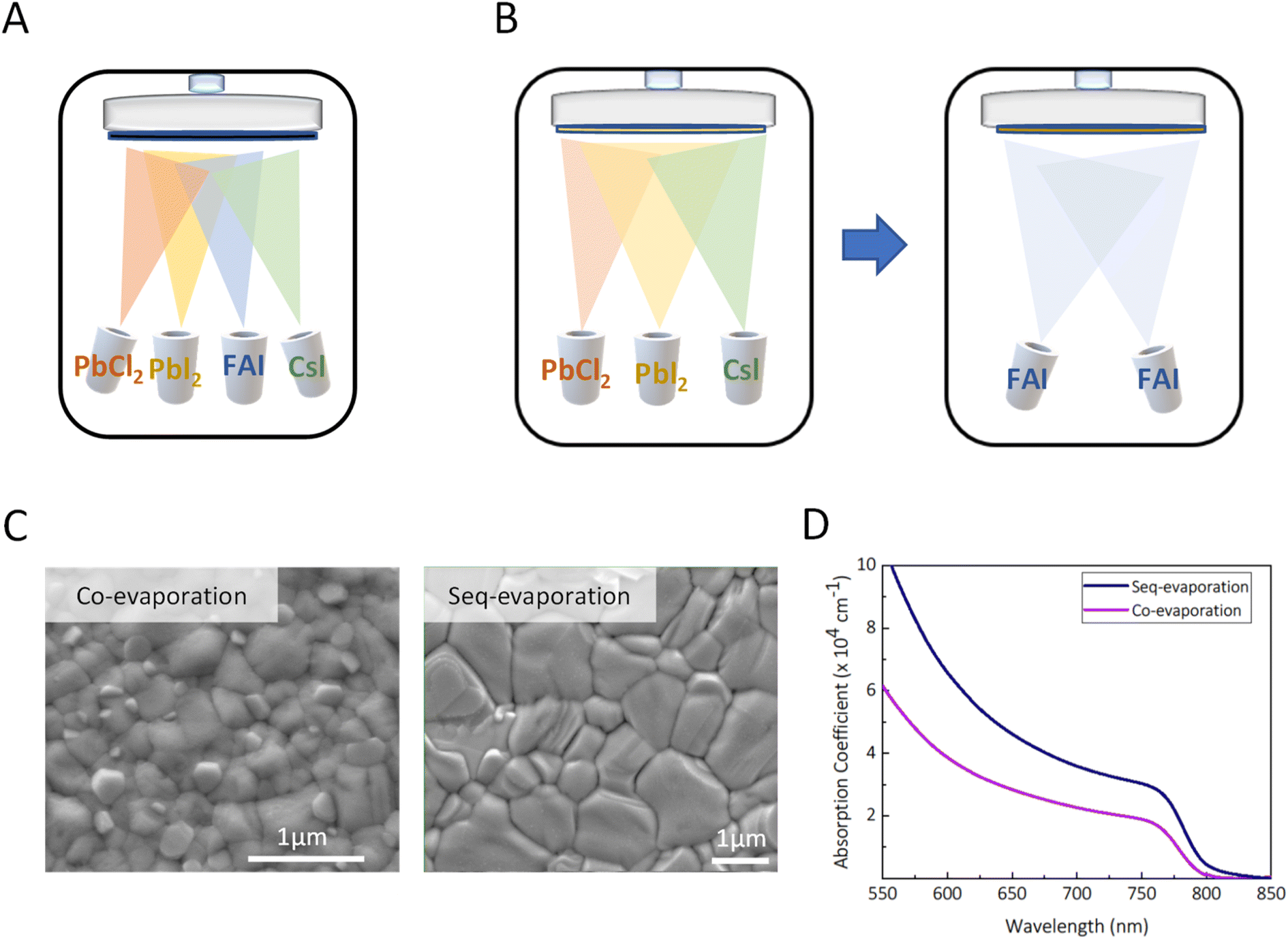 | ||
| Fig. 1 (a) Schematic of co-evaporation; (b) schematic of sequential evaporation (c) SEM top micrograms of co-evaporation and sequential deposition, respectively; (d) absorption coefficient from UV-vis of films performed on sequentially evaporated and co-evaporated half stacks. | ||
Although perovskite solar cells are susceptible to degradation in the presence of moisture, there have been many reports of improved photophysical properties and device performance when forming the perovskite crystallization under a controlled humidity atmosphere.12,17,18 While the impact of relative humidity (RH) on solution-processed devices has been extensively investigated,18,19 its influence on thermally deposited perovskite layers is not well understood. Here, we present a comprehensive study on the crystallization dynamics of sequentially vacuum-deposited perovskite films under controlled environmental conditions. We deposit an inorganic precursor layer by co-evaporating cesium iodide (CsI), lead iodide (PbI2), and lead chloride (PbCl2) to form Cs0.15Pb(I0.80Cl0.20)2.15, followed by the deposition of formamidinium iodide (FAI) onto this precursor film at room temperature, to eventually form an ABX3 perovskite structure. Exposing the films to controlled relative humidity during annealing enhances interdiffusion and homogenization of the precursors, particularly cesium and formamidinium cations throughout the bulk, which improves the photophysical properties of the perovskite material. The resulting films exhibit a photoluminescence quantum yield (PLQY) of 6% with a bandgap of 1.55 eV and enable power conversion efficiencies of 21.0% in PSCs. Devices processed under optimal humidity conditions demonstrate enhanced stability, maintaining more performance over 300 hours under accelerated aging (ISOS-L-2), as compared to those processed in the absence of humidity.
Results and discussion
The perovskite solar cells that we investigate in this study are fabricated with an all thermally evaporated layer stack of: glass/indium-tin-oxide (ITO)/2,2′,7,7′-tetrakis(N,N′-di-p-methylphenylamino)–9,9′-spirobifluorene (Spiro-TTB)/perovskite/C60/bathocuproine (BCP)/silver (Ag), where Spiro-TTB is the hole transport layer (HTL) and C60 is the electron transport layer (ETL). For the stability analysis, the top layers of the stack are changed from a BCP/Ag bilayer to a tin oxide SnOx (deposited via ALD)/chromium (Cr)/gold (Au) layer. In order to assess the morphology and optical density of the crystallised perovskite films, fabricated from co-evaporation and sequential deposition, we deposited the perovskite on a Spiro-TTB coated ITO-glass, which we refer to as “half-stacks” and characterise these films. In Fig. 1(C) we show top-view scanning electron microscope (SEM) micrographs, which reveal that the sequential deposition route results in SEM polycrystalline domains of over 1 micron, which tend to be larger as compared to those in the co-evaporated perovskite films. Furthermore, we perform ultraviolet-visible-near-infrared (UV-vis-NIR) absorptance measurements Fig. 1(D) for both sequentially evaporated and co-evaporated half stacks of the same thickness and show the absorption coefficient as a function of wavelength.Structural properties of sequentially evaporated thin films after annealing under controlled relative humidity
We proceed to investigate the impact of relative humidity (RH) on the morphological and crystalline properties of the sequentially evaporated perovskite films. We studied sequentially evaporated films that have undergone annealing under varying conditions: 0% RH (nitrogen glovebox environment, <1 ppm H2O) and the introduction of 5%, 35%, and 60% RH through compressed dry air (CDA) carrier gas into a chamber where films are annealed. We note that the RH value is in the annealing atmosphere at room temperature, not at the temperature of the annealing hotplate. The top-view SEM images in Fig. S1,† are for films fabricated under 0%, 5%, 35%, and 60% relative humidity. We observe that top-view micrographs of films annealed under 0% RH and 5% RH exhibit no overt morphological differences. Yet, with increasing relative humidity, a significant increase in polycrystalline domain size becomes evident, as viewed via top-view Fig. S1(C).† This pattern extends to higher RH levels, albeit accompanied by the emergence of pinholes in the post-annealed films Fig. S1(D),† leading to potential shunting pathways when integrated into devices.Micrograph's Fig. 2(A) and (B) unveil the cross-sectional view of films annealed in 0% RH and at 35% relative humidity. Notably, the nitrogen-annealed film shows multiple grain boundaries, as visible in the SEM image, throughout the thickness of the film. In contrast, the films annealed under ambient conditions show a monolithic grain structure from top to bottom. Noteworthy, is the discernible presence of bright crystallites at the buried interface of nitrogen-annealed films, potentially signifying unconverted inorganic precursors. In our study, we employed X-ray diffraction (XRD) analysis to substantiate our findings. As seen in Fig. 2(C), we show an X-ray diffraction (XRD) pattern of a film annealed in 0% RH environment that has retained a significant amount of residual lead iodide. A 12.7° 2θ diffraction peak corresponds to a presence of crystalline PbI2, while the 14° peak corresponds to the (100) plane of (pseudo) cubic metal halide perovskite structure. Moreover, films annealed under relative humidity display a higher overall scattering intensity and a narrower full width half maximum (FWHM) of the perovskite peak, 0.10 compared to films annealed under 0% RH with a FWHM of 0.15. We interpret this to indicate a higher fraction of the film composed of crystalline material with less micro-strain in the 35% RH annealed films, as compared to when annealed in nitrogen. To delve deeper into the crystallization kinetics, we conduct in situ laboratory and synchrotron-based grazing incidence wide angle X-ray scattering (GIWAXS) measurements monitoring the phase conversion processes from precursor films. Beginning with the unannealed film Fig. S2,† we find it already contains some perovskite phase, which has evidentially formed at the inorganic template and FAI interface at room temperature. In addition, in the as-deposited films we find PbI2, well as δ-CsPbI3; the latter was not observed in previous work using a lower content of CsI.12,20,21 We observe that the orthorhombic δ-CsPbI3, at 2θ of 9.7° and 12.6°, disappears during temperature ramping to 150 °C after around 100 s Fig. S3.† In high-resolution synchrotron measurements, we monitored the intensity of the perovskite (100) peak over 15 minutes of annealing and observed that ambient air (∼35% RH) accelerates the formation of the perovskite phase from the precursor film, as compared to annealing under 0% RH Fig. 2(D). To explore this further, we monitored the unannealed film left in ambient air and found that even at room temperature, the template and organic perovskite salts convert to a 2H hexagonal polytype phase of formamidinium rich perovskites over 40 minutes Fig. S4.†
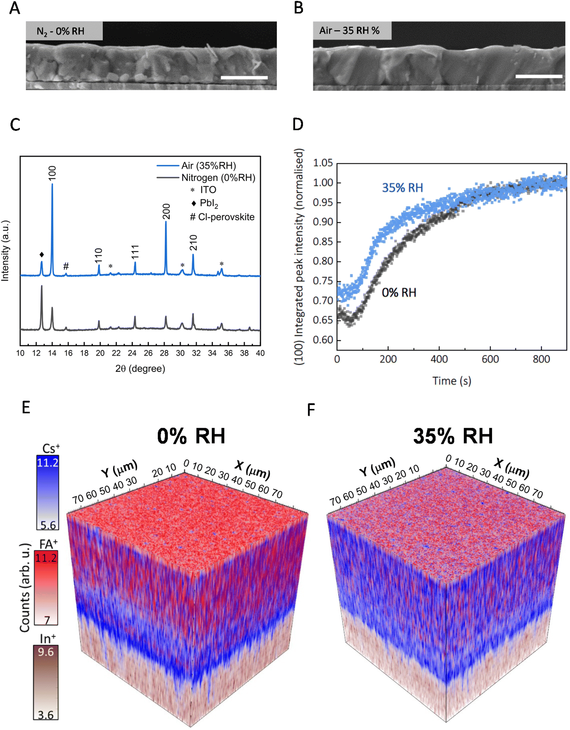 | ||
| Fig. 2 (a and b) SEM micrographs of sequentially deposited perovskite annealed in nitrogen (0% RH) and under 35% relative humidity in the humidity-controlled chamber (RH-annealed), respectively, the scale bar is 1 μm. (c) XRD of films annealed nitrogen (0% RH) and 35% RH (d) in situ tracking of perovskite formation via GIWAX of films annealed in nitrogen (0% RH) and 35% RH (e) 3D-ToF-SIMS depth profiling across 100 × 100 am for films annealed under nitrogen (0%RH) and (f) under 35% RH condition, showing the molecular fragment from cesium (Cs+, m/z = 132.91, blue) and formamidinium (FA+, m/z = 45.04, red) cations. The substrate signal from Indium (In+, m/z = 114.91) in ITO is shown in brown. | ||
To elucidate the interdiffusion dynamics of organic and inorganic precursors within thin films under dry and humid processing conditions, we employed time-of-flight secondary ion mass spectrometry (ToF-SIMS) depth profiling. This choice stems from its high detection sensitivity (<ppm) and good mass resolution, aligning with the investigative approach established by Harvey et al.,22 who initially probed differences in cation distribution within the bulk of the film. We collected both positive and negative ions from two distinct 100 × 100 micron regions on our samples Fig. S5.† In Fig. 2(E) and (F), we show the variation along the film depth of the molecular fragments' associates with perovskites' cesium (Cs+, m/z = 132.91) and formamidinium (FA+, m/z = 45.04) positive ions.23 The 3D maps are reconstructed frame to frame for a total of 25 frames Fig. S6;† the perovskite signals end at frame 17. In Fig. 2(E), we show that films annealed in 0% RH have a formamidinium-rich (red) perovskite at the top surface of the film, along with a cesium-rich (blue) perovskite at the bottom interface with ITO. This suggests that films annealed under 0% RH have precursor salts that are not entirely inter-diffused throughout the thickness of the film.
On the other hand, in Fig. 2(F), we show that films grown under controlled relative humidity conditions (35% RH) exhibit high levels of intermixing of cesium and formamidinium cations throughout the film. We performed a more quantitative assessment by calculating the standard deviation of the 2D normalized signal intensity for each molecular fragment Fig. S7.† We found that the standard deviation (σ) for both formamidium (FA+σ = 0.038) and cesium (Cs+σ = 0.037) are lower under controlled relative humidity compared to formamidinium (FA+σ = 0.054) and cesium (Cs+σ = 0.044) under 0% RH, underscoring the efficacy of this condition in promoting precursor interdiffusion. We show that this trend extends to halide ions, as depicted in Fig. (S8 and S9†). Examination of chloride precursor signals reveals a pronounced presence of Cl− ions between the bottom (buried) and at the top interface of the film for perovskite films processed in both 0% RH and 35% RH. This indicates that the Cl− ions or PbCl2 predominately accumulates at the surfaces. For the 35% RH film, the chloride ion (Cl− and PbCl3−) signals are very low and flat throughout the bulk region. In contrast, the chloride ion signals monotonically increase from around 100 nm depth towards the bottom surface for the 0% RH annealed films. Once again, we quantified this by calculating the standard deviation of lead chloride (PbCl3−) (and lead iodide (PbI+)) throughout the films, which we show in Fig. S10.† In summary, our ToF-SIMS depth profiling analysis highlights how annealing sequentially deposited perovskite films in the presence of humidity facilitates the effective interdiffusion of precursor salts and the realisation of compositionally homogeneous perovskite films, in the direction perpendicular to the substrate. We also speculate that since the chloride ions predominantly accumulate at the surfaces, they may act to passivate surface defects, which will be explored in more detail below.
Photophysical properties of sequentially evaporated perovskite films
To explore the influence of relative humidity on the photophysical properties of sequentially evaporated and co-evaporated perovskite films, we performed photoluminescence quantum yield (PLQY) measurements on perovskite thin films deposited on glass (see ESI† for details on the methods). PLQY serves as a useful metric due to its direct correlation with the quasi-Fermi level splitting (QFLS)24 and consequently open-circuit voltage (Voc) of a photovoltaic device.25,26 In Fig. 3(A) we present the PLQY measured for perovskite films deposited on glass with a PV bandgap of ∼1.55 eV, annealed under varying conditions of relative humidity. For completeness, we include both co-evaporated and sequentially evaporated thin films here. Notably, for the films produced through sequential deposition, a low PLQY of 0.12 ± 0.09% is observed when annealed in N2, compared to co-evaporated films that exhibit a slightly higher PLQY of 0.32 ± 0.03%. When annealing in the presence of humidity, the PLQY of the co-evaporated does not increase, and even diminishes slightly with values of 0.26 ± 0.02%, 0.4 ± 0.12%, and 0.30 ± 0.05% for the 5% RH, 35% RH, and 60% RH respectively. However, the sequentially evaporated films exhibit more than an order of magnitude enhancement in luminescence intensity. We determine the PLQY values to be 5.3 ± 0.4%, 5.9 ± 0.2%, and 1.3 ± 0.6% for the 5% RH, 35% RH, and 60% RH samples, respectively. As aforementioned, this substantial increase in PLQY leads to an increase in QFLS. In this context, the radiative limit (QFLSrad) for a single junction absorber with a bandgap of 1.55 eV is 1.26 eV.27 We estimate that co-evaporated films can only achieve a maximum QFLS of 1.12 eV. In contrast, films made through sequential deposition attain a maximum QFLS of 1.19 eV, which is 94% of its radiative limit. | ||
| Fig. 3 (A) PLQY of sequentially evaporated and co-evaporated films on glass fabricated under 0% RH, 5% RH, 35% RH and 60% RH, three distinct areas were measured per substrate, the error bars represent the min and max PLQY obtained. (B) TRPL of sequentially deposited perovskite films on glass under 0% RH, 5% RH, 35% RH and 60% RH. The films were photoexcited from the air-exposed side of the perovskite. (C) Median of surface and bulk non radiative recombination obtained from fitting the TRPL data of half-stacks annealed under varying relative humidity using a physical model and Bayesian inference, the median lies within the first and the third quartile represented by the bars. (D) Median of diffusion length of the perovskite half-stacks annealed under varying relative humidity, the median lies within the first and the third quartile represented by the bars. | ||
To further understand how the relative humidity leads to an increased PLQY, we perform time resolved photoluminescence measurements (TRPL) on a similar set of sequentially evaporated thin films annealed under the different conditions. In Fig. 3(B) a similar trend to that of PLQY is observed in the TRPL measurements: the sample annealed at 0% RH shows early-time decay of the PL, with the PL decay lifetime extending significantly for the samples annealed in humid conditions, which we quantify by fitting with a stretched exponential28 Fig. S11.† We find an average lifetime, τav, of 56 ns for the 0% RH (nitrogen-annealed) sample, which increases to 730 ns, 1000 ns, and slightly drops to 632 ns for the 5% RH, 35% RH, and 60% RH conditions, respectively. We note that from all our previous co-evaporated perovskite films reported, the longest lifetime has been ∼100 ns, with the maximum PLQY significantly less than 1%, consistent with other reports in literature,6,29 highlighting the step-change improvement this processing and annealing protocol represents.
To investigate where the main improvements in PLQY and prolonged lifetime stem from, we follow a recently developed approach employing Bayesian inference.30 In brief, TRPL decays are influenced by many parameters, including bulk-lifetime, surface recombination at both the top and bottom surfaces, and rate of charge carrier diffusion away from the surface throughout the film. By using simple analytical fitting, it is difficult to determine all the governing parameters with a high level of accuracy. However, by more advanced computation approaches, using machine learning or Bayesian inference, it is possible to accurately (with quantifiable uncertainty) determine multiple parameters from these data. Following Kober-Czerny et al.,30 we simulated the PL decay employing a physical model and Bayesian inference to discern the bulk and surface recombination parameters, as well as charge carrier diffusion coefficients. We use three TRPL measurements (one from the glass side at a fluence of 3.8 × 1010 cm−2 and two from the air, or top charge transport layer, side at fluences of 3.8 × 10⁹ and 3.8 × 1010 cm−2). In Fig. 3(C), we show the results and here report all values as M(Q1 – Q3), where M is the median value and Q1 and Q3 are the first and third quartile values. We determine non-radiative interfacial recombination constants at the Spiro-TTB/perovskite interface of 1.7 (1.7–1.9) × 107, 4.3 (3.2–4.6) × 106, 2.6 (2.4–2.8) × 106, and 2.8 (2.6–3.0) × 106 s−1 as well as non-radiative bulk recombination constants (kbulk see ESI† for details) of 2.2 (1.9–2.6) × 107, 8.8 (7.1–13.0) × 106, 2.9 (2.2–6.7) × 106, and 3.7 (3.5–4.4) × 106 s−1 for the 0% RH, 5% RH, 35% RH, and 60% RH conditions, respectively. This indicates that annealing in a humid environment strongly impacts both the surface and the bulk recombination processes, with the most significant reduction in the bulk, likely due to the reduction of bulk defects. In contrast, the perovskite/air interface is much less influenced by the humid environment, with extracted recombination constants of 8.9 (0.2–23.3) × 105, 2.0 (1.1–2.6) × 106, 1.2 (1.1–1.4) × 106, and 7.6 (5.9–8.2) × 105 s−1 for the 0% RH, 5% RH, 35% RH, and 60% RH conditions, respectively.
In the ESI† we also show the extracted vertical mobility values (vertical with respect to the substrate), which show no significant dependence on the annealing atmosphere. We obtain values between 0.2 and 0.4 cm2 V−1 s−1 for all samples Fig. (S12–S15†). This result suggests that the vertical charge diffusion is not limited by scattering nor trapping by the same defects responsible for non-radiative charge carrier recombination. In addition to estimating the charge carrier mobility via measurements of the PL decays, we have conducted optical-pump THz-probe spectroscopy to investigate if the “shorter-range” THz determined charge-carrier mobility is influenced by the annealing conditions. We show the sum of THz mobilities for electrons and holes (corresponding to in-plane motion) for the sequentially evaporated perovskite films with the different annealing conditions in Fig. S16.† Similarly, to the vertical mobility, we do not observe any significant change with annealing conditions, with the sum of THz mobilities ranging from 44 to 48 cm2 V−1 s−1. This once again suggests that the defects responsible for non-radiative recombination are not the same as those responsible for charge-carrier scattering.
Using our determined bulk charge carrier lifetime (1/kbulk) and vertical mobility derived from the PL decays, we estimate bulk diffusion lengths of 330 (300–340), 410 (350–440), 560 (390–630), and 430 (400–440) nm for the 0% RH, 5% RH, 35% RH, and 60%RH conditions, respectively Fig. 3(D). These are within the range of the film thickness and hence could influence charge collection efficiency in the solar cell. We note that these values appear to be relatively low, as compared to usually reported charge carrier diffusion lengths for metal halide perovskites. However, this is due to the method used for diffusion length estimation. For instance, if we use the short-range THz sum of charge carrier mobilities for electrons and holes, which we have determined to be ∼46 cm2 V−1 s−1 as shown in Fig. S16,† combined with the stretched exponential lifetime of 1000 ns that we estimate above for the 35% RH perovskite film, then we would estimate a diffusion length of between 7.7 μm, which is in the range of diffusion lengths estimated for state-of-the-art solution processed polycrystalline perovskite films via similar methods.31 We believe that our approach of using the PL decay to estimate the vertical mobility is more reflective of the relevant long-range charge carrier mobility and hence diffusion length in a solar cell device.
Photovoltaic performance and device stability
To corroborate the impact of the improved material quality on device performance, we integrated our sequentially evaporated perovskite films into all-vacuum processed device stacks, as seen in Fig. 4(A). The perovskite layers were post-annealed in two distinct environments: under a nitrogen glovebox environment (0% RH) and in air with controlled 35% relative humidity (35% RH). To assess the photovoltaic characteristics of these solar cells, we conducted current density–voltage (J–V) scans, maximum power point (MPP) tracking, as well as steady-state open-circuit voltage and short-circuit current measurements, as illustrated in Fig. 4(B), (C), and S18† respectively. Our 0% RH annealed champion device with an estimated bandgap of 1.56 eV from EQE as shown in Fig. S17,† exhibited a steady-state open-circuit voltage (ssVoc) of 1.016 V, a steady-state current density (ssJsc) of 21.6 mA cm−1−2, an MPP efficiency of 18.0%, and a corresponding calculated “steady-state fill factor” (ssFF) of 0.82. Encouragingly, the champion device containing a perovskite film annealed under 35% RH with an estimated bandgap of 1.55 eV from EQE as shown in Fig. S17,† measured a steady-state Voc of 1.05 V, a steady-state Jsc of 24.3 mAcm−2, a MPP efficiency of 21.0% and a calculated ssFF of 0.83. In Fig. 4(D) we show the statistical distribution of the MPP efficiency for a batch of 15 devices of each type. We observe that the mean efficiency increases from 14% to 20%, with the distribution significantly narrowing. We show external quantum efficiency (EQE) spectra for a representative 0% RH and 35% RH annealed device in Fig. 4(E), where the integrated current density of 21.3 mA cm−2 and 24.1 mA cm−2 for the solar cell fabricated under 0% RH and 35% RH closely matched the device's current density of 21.6 mA cm−2 and 24.3 mA cm−2, measured with the solar simulator. These results highlight the strong impact of controlled relative humidity during perovskite film annealing upon the photovoltaic performance, consistent with the improvement in bulk carrier diffusion length and reduced interface recombination for the 35% RH annealed devices. Importantly, the statistics we show in Fig. 4(D) also highlight the importance of this processing step upon improving the reproducibility and narrowing the performance spread in the devices. We note that from the QFLS analysis of the half-stacks, we observed an increase from 1.08 to 1.19 eV. The relatively small increase in Voc, from 1.02 to 1.05 V, may stem from the voltage being limited by the heterojunction with the electron transport material. To quantify the losses associated with the electron transport layer (ETL) contact, we performed PLQY measurements on perovskite-ETL half-devices Fig. S18.† It is evident that the n-contact, C60 fullerene interface is still the limiting contact that quenches the PLQY of sequentially evaporated perovskites by an order of magnitude, resulting in an estimated QFLS of 1.07 meV for the perovskite/ETL half-stack, closely matching the measured Voc in the complete solar cell. Clearly, future routes to improve the efficiency of all-evaporated perovskite solar cells should focus upon finding new ETLs that induce less recombination losses or passivating this interface. | ||
| Fig. 4 (A) fully vacuum deposited device stack using BCP/Silver or ALD SnO2/Cr/Au for standard solar cells and stable contacts used for stability analysis, respectively. (B) JV curves of devices fabricated where annealing is done in presence of 0% RH (nitrogen) and 35% RH. (C) Maximum power point tracking of champion devices obtained from nitrogen (0% RH) and 35% RH annealing, respectively. (D) Statistical comparison of max power point efficiency obtained from maximum point tracking. (E) External quantum efficiency of a device where the perovskite is annealed under 0% RH and 35% RH. (F) Maximum power point efficiency as a function of time for cells aged under open-circuit at elevated temperature under light (85 °C, 0.76 suns illumination from a xenon lamp aging box with no UV filter) ∼ISOS-L-2, where the perovskite was annealed under 0% RH in nitrogen and 35% RH in air. The cells were occasionally removed from the ageing rig, allowed to cool to room temperature, and measured under AM1.5100 mW cm−2 simulated sun light to determine the photovoltaic performance parameters, including the mpp efficiency. The error bars represent the median standard deviation. | ||
We proceed to test the stability of our all-vacuum processed perovskite solar cells under elevated temperature (85 °C) and full spectrum simulated sun light, held under open circuit using cells with SnOx/Cr/Au contacts, as we illustrate in Fig. 4(A). It has been reported that stress testing perovskite devices under open-circuit conditions accelerates degradation compared to MPP condition.32,33 For measuring the solar cells during ageing, we remove the cells from the ageing chamber and allow enough time to reach room temperature and then subsequently measure them under AM1.5G 100 mW cm−2 simulated sun light. We show the mpp efficiency as a function of ageing time in Fig. 4(F), where we observe that both sets of devices exhibited an initial “burn-in” phase, leading to a significant early decrease in median performance, which has also been observed in other studies.34,35 The set of devices annealed under nitrogen, experienced a substantial performance drop of ∼7% in absolute efficiency under this initial burn-in phase, whereas those fabricated at 35% RH, showed a smaller decline of ∼4% in absolute efficiency. After 200 hours of ageing, the nitrogen-annealed devices showed a 92% relative drop in performance, whereas the devices annealed under 35% RH only dropped by 32% relative to their initial median performance. Moreover, post-200 hours visual inspection revealed that devices fabricated in the absence of humidity became visibly discoloured, as depicted in Fig. S19.† Conversely, as we observe in the photographs, the cells fabricated at 35% RH maintain their pristine appearance. Further investigation to understand the degradation pathways are part of ongoing investigations. These results reveal that interdiffusion in sequentially evaporated perovskite absorbers significantly influences both photovoltaic efficiency and long-term stability.
Conclusion
In this study, we have investigated the impact of the relative humidity in the perovskite film annealing atmosphere upon the physical and optoelectronic properties, performance and stability of sequentially evaporated perovskite thin films and solar cells. Using in situ grazing incidence wide-angle X-ray scattering (GIWAXS) and time-of-flight secondary ion mass spectrometry (ToF-SIMS), we find that annealing in a controlled humid environment promotes the interdiffusion between the inorganic and organic precursors. By increasing the intermixing via humid atmosphere annealing, we obtained larger polycrystalline grain sizes, reaching up to microns, and a higher crystallinity. We also find that the humidity annealed films have reduced bulk and surface recombination and estimate a significant increase in both the PLQY, closing the gap between evaporated and solution processed perovskites, and in the corresponding bulk charge carrier diffusion lengths. These improvements in crystallographic and corresponding optoelectronic properties translated to enhanced efficiency up to 21%, and enhanced stability under full-spectrum simulated sun-light at 85 °C and open-circuit conditions. Our results demonstrate that this industry-compatible deposition technique can not only deliver high efficiencies, but also reasonably robustness devices that exhibit improved stability under long-term accelerated aging. We expect that this study will pave the way for future efforts on all-evaporated perovskite solar cells, where we have especially identified the interface between the perovskite and the top electron-transport material, C60, as the most limiting component for efficiency. Despite having demonstrated enhanced stability here, with the humidity annealed PSCs, future work should also focus upon understanding and resolving the instabilities which still exist in the all-vapour-deposited PSCs.Author contributions
The manuscript was written through the contributions of all authors. All authors have given approval to the final version of the manuscript. RAN and HJS conceived the idea. RAN, HJS, and DPM designed the experiments. RAN fabricated the fully vacuum deposited solar cells and samples for material characterisation. Current–voltage characteristics, EQE measurements and stability measurements for solar cells were performed by RAN. Film thicknesses, absorbance spectra, photoluminescence quantum yield, and time-resolved photoluminescence decay profiles were measured by RAN, MKC, AD and PC. A physical model of TRPL fitting was developed by MKC. X-ray diffraction was performed by RAN and JAS. Ex situ and in situ grazing incidence wide angle X-ray scattering measures and analysis were conducted by JAS. Time of flight secondary ion mass spectrometry measurements were performed by DJG. Analysis of 3D time of flight secondary ion mass spectrometry data was performed by MT, supervised by DG. Scanning electron micrograms were obtained by RAN, AK, and BWP. OPTP was performed by KAE supervised by LMH. Atomic layer deposition for tin oxide was set up by JW and SS. National thin film cluster facility service, maintenance and working up of deposition recipes was performed by JY. The project was supervised by HJS.Data availability
Data for this manuscript will be available via the University of Oxford Research Archive, https://ora.ox.ac.uk/.Conflicts of interest
Henry J. Snaith is a co-founder and Chief Scientific Officer of Oxford Photovoltaics, Ltd. M. Greyson Christoforo is a co-founder and co-CEO of Ark Metrica, Ltd.Acknowledgements
This work was part funded by UK Research and Innovation (UKRI) under the UK government's Horizon Europe funding guarantee [grant number 10055025], the engineering and physical sciences research council (EPSRC) UK, under grant EP/V027131/1, the office of naval research (ONR) and ONR-global (Award # N00014-20-1-2587), and the DFG via the SPP2196 Priority Program (CH 1672/3-1). The authors acknowledge the EPSRC National Thin Film Facility for Advanced Functional Materials (NTCF), EP/M022900/1, hosted by the Department of Physics at the University of Oxford and part funded by the Wolfson Foundation. We acknowledge Diamond Light Source for time on beamline I07 under proposal SI33462-1 for the GIWAXS measurements and thank Fengning Yang and Jonathan Rawle for assistance with these measurements, and Karl-Augustin Zaininger for assistance with the experimental setup design. We also thank Moritz Riede, Nakita K. Noel, and Sebastian R. Bonilla for useful discussions. RAN thanks the Oxford Clarendon scholarship and the Binks Trust for their generous sponsorship of his studentship.References
- NREL, NREL Interactive Best Research-Cell Efficiency Chart, https://www.nrel.gov/pv/interactive-cell-efficiency.html.
- N. M. Haegel, P. Verlinden, M. Victoria, P. Altermatt, H. Atwater, T. Barnes, C. Breyer, C. Case, S. De Wolf, C. Deline, M. Dharmrin, B. Dimmler, M. Gloeckler, J. C. Goldschmidt, B. Hallam, S. Haussener, B. Holder, U. Jaeger, A. Jaeger-Waldau, I. Kaizuka, H. Kikusato, B. Kroposki, S. Kurtz, K. Matsubara, S. Nowak, K. Ogimoto, C. Peter, I. M. Peters, S. Philipps, M. Powalla, U. Rau, T. Reindl, M. Roumpani, K. Sakurai, C. Schorn, P. Schossig, R. Schlatmann, R. Sinton, A. Slaoui, B. L. Smith, P. Schneidewind, B. Stanbery, M. Topic, W. Tumas, J. Vasi, M. Vetter, E. Weber, A. W. Weeber, A. Weidlich, D. Weiss and A. W. Bett, Science, 2023, 380, 39–42 CrossRef CAS PubMed.
- M. Liu, M. B. Johnston and H. J. Snaith, Nature, 2013, 501, 395–398 CrossRef CAS PubMed.
- E. Aydin, T. G. Allen, M. De Bastiani, A. Razzaq, L. Xu, E. Ugur, J. Liu and S. De Wolf, Science, 2024, 383, eadh3849 CrossRef CAS PubMed.
- T. Abzieher, D. T. Moore, M. Roß, S. Albrecht, J. Silvia, H. Tan, Q. Jeangros, C. Ballif, M. T. Hoerantner and B.-S. Kim, Energy Environ. Sci., 2024, 17, 1645–1663 RSC.
- K. B. Lohmann, J. B. Patel, M. U. Rothmann, C. Q. Xia, R. D. J. Oliver, L. M. Herz, H. J. Snaith and M. B. Johnston, ACS Energy Lett., 2020, 5, 710–717 CrossRef CAS PubMed.
- J. B. Patel, A. D. Wright, K. B. Lohmann, K. Peng, C. Q. Xia, J. M. Ball, N. K. Noel, T. W. Crothers, J. Wong-Leung, H. J. Snaith, L. M. Herz and M. B. Johnston, Adv. Energy Mater., 2020, 10, 1903653 CrossRef CAS.
- M. Roß, L. Gil-Escrig, A. Al-Ashouri, P. Tockhorn, M. Jost, B. Rech and S. Albrecht, ACS Appl. Mater. Interfaces, 2020, 12, 39261–39272 CrossRef PubMed.
- C. Momblona, L. Gil-Escrig, E. Bandiello, E. M. Hutter, M. Sessolo, K. Lederer, J. Blochwitz-Nimoth and H. J. Bolink, Energy Environ. Sci., 2016, 9, 3456–3463 RSC.
- J. Li, H. Wang, X. Y. Chin, H. A. Dewi, K. Vergeer, T. W. Goh, J. W. M. Lim, J. H. Lew, K. P. Loh, C. Soci, T. C. Sum, H. J. Bolink, N. Mathews, S. Mhaisalkar and A. Bruno, Joule, 2020, 4, 1035–1053 CrossRef CAS.
- J. Ávila, C. Momblona, P. P. Boix, M. Sessolo and H. J. Bolink, Joule, 2017, 1, 431–442 CrossRef.
- H. Li, J. Zhou, L. Tan, M. Li, C. Jiang, S. Wang, X. Zhao, Y. Liu, Y. Zhang, Y. Ye, W. Tress and C. Yi, Sci. Adv., 2022, 8, eabo7422 CrossRef PubMed.
- J. Zhou, L. Tan, Y. Liu, H. Li, X. Liu, M. Li, S. Wang, Y. Zhang, C. Jiang, R. Hua, W. Tress, S. Meloni and C. Yi, Joule, 2024, 8(6), 1691–1706 CrossRef CAS.
- H. Li, L. Tan, C. Jiang, M. Li, J. Zhou, Y. Ye, Y. Liu and C. Yi, Adv. Funct. Mater., 2023, 33, 2211232 CrossRef CAS.
- M. Kam, Y. Zhu, D. Zhang, L. Gu, J. Chen and Z. Fan, Sol. RRL, 2019, 3, 1900050 CrossRef.
- S. Wang, L. Tan, J. Zhou, M. Li, X. Zhao, H. Li, W. Tress, L. Ding, M. Graetzel and C. Yi, Joule, 2022, 6, 1344–1356 CrossRef CAS.
- X. Y. Chin, D. Turkay, J. A. Steele, S. Tabean, S. Eswara, M. Mensi, P. Fiala, C. M. Wolff, A. Paracchino, K. Artuk, D. Jacobs, Q. Guesnay, F. Sahli, G. Andreatta, M. Boccard, Q. Jeangros and C. Ballif, Science, 2023, 381, 59–63 CrossRef CAS PubMed.
- G. E. Eperon, S. N. Habisreutinger, T. Leijtens, B. J. Bruijnaers, J. J. van Franeker, D. W. deQuilettes, S. Pathak, R. J. Sutton, G. Grancini, D. S. Ginger, R. A. Janssen, A. Petrozza and H. J. Snaith, ACS Nano, 2015, 9, 9380–9393 CrossRef CAS PubMed.
- J. You, Y. Yang, Z. Hong, T.-B. Song, L. Meng, Y. Liu, C. Jiang, H. Zhou, W.-H. Chang, G. Li and Y. Yang, Appl. Phys. Lett., 2014, 105(18), 183902 CrossRef.
- O. Er-Raji, A. J. Bett, S. Lange, H. Nagel, M. Bivour, O. Schultz-Wittmann, C. Hagendorf, M. Hermle, J. Borchert, S. W. Glunz and P. S. C. Schulze, Prog. Photovolt.: Res. Appl., 2023, 7, 24 Search PubMed.
- Q. Guesnay, F. Sahli, K. Artuk, D. Turkay, A. G. Kuba, N. Mrkyvkova, K. Vegso, P. Siffalovic, F. Schreiber, H. Lai, F. Fu, M. Ledinský, N. Fürst, A. Schafflützel, C. Bucher, Q. Jeangros, C. Ballif and C. M. Wolff, Adv. Energy Mater., 2024, 14, 2303423 CrossRef CAS.
- S. P. Harvey, Z. Li, J. A. Christians, K. Zhu, J. M. Luther and J. J. Berry, ACS Appl. Mater. Interfaces, 2018, 10, 28541–28552 CrossRef CAS PubMed.
- M. Taddei and D. J. Graham, Surf. Sci. Spectra, 2024, 31, 015004 CrossRef CAS.
- P. K. Nayak, S. Mahesh, H. J. Snaith and D. Cahen, Nat. Rev. Mater., 2019, 4, 269–285 CrossRef CAS.
- P. Caprioglio, M. Stolterfoht, C. M. Wolff, T. Unold, B. Rech, S. Albrecht and D. Neher, Adv. Energy Mater., 2019, 9, 1901631 CrossRef.
- U. Rau, Phys. Rev. B:Condens. Matter Mater. Phys., 2007, 76, 085303 CrossRef.
- S. Rühle, Sol. Energy, 2016, 130, 139–147 CrossRef.
- M. Taddei, S. Jariwala, R. J. E. Westbrook, S. Gallagher, A. C. Weaver, J. Pothoof, M. E. Ziffer, H. J. Snaith and D. S. Ginger, ACS Energy Lett., 2024, 9, 2508–2516 CrossRef CAS.
- K. B. Lohmann, S. G. Motti, R. D. J. Oliver, A. J. Ramadan, H. C. Sansom, Q. Yuan, K. A. Elmestekawy, J. B. Patel, J. M. Ball, L. M. Herz, H. J. Snaith and M. B. Johnston, ACS Energy Lett., 2022, 7, 1903–1911 CrossRef CAS PubMed.
- M. Kober-Czerny, A. Dasgupta, S. Seo, F. M. Rombach, D. P. McMeekin, H. Jin and H. J. Snaith, PRX Energy, 2025, 4, 013001 CrossRef.
- G. Hodes and P. V. Kamat, J. Phys. Chem. Lett., 2015, 6, 4090–4092 CrossRef CAS PubMed.
- M. V. Khenkin, K. M. Anoop, E. A. Katz and I. Visoly-Fisher, Energy Environ. Sci., 2019, 12, 550–558 RSC.
- K. Domanski, E. A. Alharbi, A. Hagfeldt, M. Grätzel and W. Tress, Nat. Energy, 2018, 3, 61–67 CrossRef CAS.
- Y.-H. Lin, F. Yang, X.-L. Cao, A. Dasgupta, R. D. J. Oliver, A. M. Ulatowski, M. M. McCarthy, X. Shen, Q. Yuan, M. G. Christoforo, F. S. Y. Yeung, M. B. Johnston, N. K. Noel, L. M. Herz, M. S. Islam and H. J. Snaith, Science, 2024, 384, 767–775 CrossRef CAS PubMed.
- Z. Iqbal, R. Félix, A. Musiienko, J. Thiesbrummel, H. Köbler, E. Gutierrez-Partida, T. W. Gries, E. Hüsam, A. Saleh, R. G. Wilks, J. Zhang, M. Stolterfoht, D. Neher, S. Albrecht, M. Bär, A. Abate and Q. Wang, J. Am. Chem. Soc., 2024, 146, 4642–4651 CrossRef CAS PubMed.
Footnote |
| † Electronic supplementary information (ESI) available. See DOI: https://doi.org/10.1039/d5el00017c |
| This journal is © The Royal Society of Chemistry 2025 |