
 Open Access Article
 This Open Access Article is licensed under a Creative Commons Attribution-Non Commercial 3.0 Unported Licence
Elucidating the role of heterojunction in pristine non-fullerene acceptor organic solar cells†
Anirudh
Sharma
 *a,
Julien
Gorenflot
a,
Han
Xu
a,
José P.
Jurado
a,
Shahidul
Alam‡
a,
Diego
Rosas Villalva
a,
Xun
Pan
b,
Jules
Bertrandie
a,
Prem D.
Nayak
a,
Yakun
He
a,
Maryam
Alqurashi
a,
Ying
Luo
a,
Mats R.
Andersson
b,
Oskar J.
Sandberg
c,
Frederic
Laquai‡
a and
Derya
Baran
*a
*a,
Julien
Gorenflot
a,
Han
Xu
a,
José P.
Jurado
a,
Shahidul
Alam‡
a,
Diego
Rosas Villalva
a,
Xun
Pan
b,
Jules
Bertrandie
a,
Prem D.
Nayak
a,
Yakun
He
a,
Maryam
Alqurashi
a,
Ying
Luo
a,
Mats R.
Andersson
b,
Oskar J.
Sandberg
c,
Frederic
Laquai‡
a and
Derya
Baran
*a
aMaterials Science and Engineering Program (MSE), Physical Science and Engineering Division (PSE), King Abdullah University of Science and Technology (KAUST), Thuwal 23955-6900, Kingdom of Saudi Arabia. E-mail: anirudh.sharma@kaust.edu.sa; derya.baran@kaust.edu.sa
bFlinders Institute for Nanoscale Science and Technology, College of Science and Engineering, Flinders University, Bedford Park 5042, Australia
cPhysics, Faculty of Science and Engineering, Åbo Akademi University, Henrikinkatu 2, Turku 20500, Finland
First published on 25th June 2025
Abstract
Non-fullerene acceptors (NFAs) are rapidly transforming organic solar cell (OSC) performance and stability, yet the operational principles of pristine NFA devices remain underexplored. Here, we reveal that interfacial energetics, rather than bulk properties, dominate charge generation and recombination in pristine NFA-based photoactive layers (PALs). Although recent studies suggest spontaneous charge generation within the NFA bulk, our findings demonstrate that charge generation and extraction predominantly occur at the hole transport layer (HTL)/NFA interface, mimicking bilayer device behavior. Moreover, while CuSCN forms favorable interfaces that sustain long-lived charges and enhance photocurrent, PEDOT:PSS exhibits poor energy level alignment and a high trap density, leading to severe recombination losses via triplet exciton formation. Introducing as little as 2 wt% donor polymer surpasses the PAL percolation threshold, forming donor–acceptor interfaces that enhance photon utilization, reduce injection barriers, and improve charge transport. Our results not only challenge current interpretations of charge generation in pristine NFA devices but also establish new design principles for simplified, scalable single-component OSCs suited for next-generation semitransparent photovoltaics, including building-integrated photovoltaics (BIPV) and agrivoltaics.
Broader contextAccelerating the global shift to clean, sustainable energy is critical to mitigating climate change and reducing dependence on fossil fuels. Organic solar cells (OSCs) offer a compelling path forward due to their lightweight, flexible form factors and scalable, low-cost processing. The development of non-fullerene acceptors (NFAs) has driven major advances in OSC efficiency, with recent studies—particularly on Y6—suggesting the potential for charge generation without donor materials. However, mechanistic understanding of these processes remains incomplete. In this work, we present a detailed investigation of pristine L8BO, a leading NFA in the Y6 molecular family. Our findings provide direct evidence that charge generation in pristine L8BO occurs not intrinsically, but at the interface with charge transport layers (CTLs), behaving like a bilayer system. We show that semiconducting CTLs enable efficient charge separation, while metal-like CTLs accelerate recombination via triplet-state formation. Introducing a small amount of donor polymer enhances interfacial energetics, significantly improving performance. These results refine the emerging understanding of NFA-based devices, highlighting interfacial processes as key to their function. The insights presented here will inform the rational design of more efficient, simplified OSCs and guide broader optoelectronic applications critical to the clean energy transition. |
Introduction
The emergence of high-performing non-fullerene acceptors (NFA) has provided an essential impetus to the power conversion efficiencies (PCEs) of organic solar cells (OSCs), now exceeding 20% for bulk heterojunction (BHJ) devices.1 The high PCEs of NFA-based OSCs are often attributed to the complementary absorption of NFAs to the donor materials,2 relatively long exciton diffusion length,3 as well as the low exciton binding energy of NFAs.4In organic semiconductors, light absorption usually forms excitons due to the low dielectric constant of those materials. Hence, most high-performing OSCs utilize a BHJ, which is necessary to efficiently split excitons into free charges and overcome the limited exciton diffusion length of most traditional organic semiconductors. Such BHJ is composed of an electron-donating (lower electron affinity) and an electron-accepting (higher electron affinity) material blended in the photoactive layer (PAL), where the energetic offsets between the donor (D) and acceptor (A) dictate free charge generation4,5 and voltage losses.6 Critically, at the D/A interface, those energetics are strongly influenced by the interaction of charges with the strong quadrupole moments of modern NFA molecules.7
Recently, pristine Y6 has been reported to generate photoinduced charges without the assistance of a donor material.8 Consequently, functional OSCs were demonstrated using pristine Y6 as the PAL, though the performance varied significantly across different reports.8,9 More recently, we showed that photoinduced charges can also be generated in other NFAs.10 It is tentatively believed that the varying local energetics of A–D–A type NFAs favor the splitting of the excitons, facilitating charge generation.10,11 However, careful analysis of OSCs using Y6 PAL shows that the PCEs of these devices depend significantly on the hole transport layer (HTL) used. For example, OSCs with pristine Y6 as the PAL and MoOx,12 PEDOT:PSS,8 PCP-Na,8 and CuSCN9 as the HTL resulted in PCEs of 0.05%, 0.09%, 0.63%, and 4.4%. Eisner et al. have also shown the presence of emissive charge-transfer (CT) states between CuSCN and organic acceptor molecules, which is believed to facilitate charge generation.13
Furthermore, in a BHJ configuration, unipolar charge extraction is achieved: NFA being the high electron affinity (EA) material, its EA energetically aligns with the electron transport layer (ETL),14,15 whereas for the donor material with lower ionization energy (IE), its IE aligns energetically with the HTL. Intuitively, in devices with pristine NFA as the PAL, the alignment between the IE of the NFA and the HTL would also be crucial for efficient hole selectivity and extraction.
While it is evident that CuSCN facilitate better performing OSCs with NFA as the only PAL, the field is imperatively lacking a conclusive mechanistic understanding about (a) what makes CuSCN superior for NFA only OSCs, compared with other commonly used HTLs such as PEDOT:PSS that perform well in bulk-heterojunction devices but not NFA only, (b) does spontaneous charge generation really happens in the bulk of pristine NFA or does it primarily happen at the HTL/NFA interface, (c) are small photoinduced charge signals observed spectroscopically usable for devices, and (d) does the HTL–NFA interface play a role in charge recombination limiting photocurrent generation?
Zhang et al.,16 demonstrating Y6 devices with CuSCN interpreted the non-zero EQE in the entire absorption range of Y6 as an evidence of spontaneous charge generation in Y6. However, when CuSCN is replaced with PEDOT:PSS as the HTL, the EQE drops from a maximum of ∼25% to just over 1%, making the authors conclude that unlike CuSCN, the PEDOT:PSS interface with NFA does not facilitate free charge generation. Importantly, this study again points towards an important role CuSCN plays in such devices.
On the other hand, it has also been shown that adding small amounts of donor polymer to NFAs can significantly enhance the charge generation in NFAs,8,10,16 and consequently the device performance.17 Dolan and colleagues have recently shown that adding only 1% of a donor polymer PIDT-T8BT to Y6 can significantly enhance the short-circuit current (JSC) from 0.28 mA cm−2 to 7.82 mA cm−2.12 The above findings challenge our current understanding of how NFA-based OSCs work. It is therefore necessary to systematically investigate and understand the role of the donor materials, and the HTL in the photo-physical processes of charge generation and recombination in pristine NFA solar cells.
In this work, we study OSCs based on pristine L8BO, an NFA from the Y-family with branched alkyl side chains,18 chosen for its exciton diffusion length that exceeds that of Y619 and anticipated morphology-induced energy cascade, making it a good candidate to probe free charge generation.9 Experimental findings and electro-optical simulations show that exciton dissociation and charge generation in pristine L8BO primarily takes place close to the hole transport layer (HTL)–PAL heterojunction when CuSCN or PEDOT:PSS is used as the HTL. However, we show that due to the unfavorable energetics for L8BO devices, PEDOT:PSS acts as a recombination site, in line with the outcomes of our drift-diffusion simulations. As a result, photoinduced charges in L8BO quickly recombine into triplets, severely affecting the device performance. In contrast, L8BO devices with CuSCN as the HTL predominantly form free charges which are long-lived, as a result, OSCs with PCE of 4.2% were achieved. Addition of <5 wt% PM6 to L8BO further enhanced the PCE to 7.9%. The results demonstrate that utilizing an energetically favorable HTL as a heterojunction or the presence of a trace amount of donor polymer is significant and necessary to achieving long-lived charges by facilitating charge generation and suppressing charge recombination.
Results and discussion
Impact of HTL energetics in L8BO devices
We fabricated OSCs using pristine L8BO as the PAL, and CuSCN and PNDIT-F3N as the HTL and ETL respectively, and demonstrated a PCE of 4.2% (Fig. 1(A), Table 1; see Table S1, ESI† for statistical data from over 20 devices). It is noteworthy that, an OSC device based on pristine L8BO PAL, resulted in JSC of 7.9 mA cm−2, an open-circuit voltage (VOC) of over 0.86 V, and a fill factor (FF) of 61%. This is consistent with previously reported pristine Y6 devices.9 In contrast, when CuSCN was replaced with PEDOT:PSS as the HTL, L8BO devices performed poorly with drastically reduced photovoltaic parameters (Fig. S1 and Table S1, ESI†) JSC of 0.09 mA cm−2, VOC of over 0.74 V and 27% FF, resulting in a negligible PCE of 0.02%. Similarly, 2PACz and Br-2PACz interlayers,20 when utilized instead of CuSCN, resulted in PCEs of 0.08% and 0.05%, respectively (Fig. S1 and Table S1, ESI†). This strongly demonstrates the significant role the HTL plays in achieving L8BO devices with a reasonable performance. | ||
Fig. 1 Photovoltaic and electrical characterization reveals that non-geminate recombination limits the fill factor, and PEDOT:PSS acts as a charge recombination site in L8BO solar cells. (A) J–V curve of L8BO device and the total generated charge measured using time-delayed collection field (TDCF) as a function of applied bias. Inset shows the structure of L8BO devices. (B) Energy level alignment of L8BO with CuSCN. (C) Energy level alignment of L8BO with PEDOT:PSS. The energy levels determined from UPS and LE-IPES measurements have been rounded to the nearest decimal digits. The reproducibility of UPS and LE-IPES measurements including experimental uncertainty is approximately ±0.1 eV. (D) External quantum efficiency (EQEpv) and electroluminescence (EL) spectra of L8BO OSCs with CuSCN. The EQEpv was determined using sensitive EQE and reconstructed from EL (below ∼ 1 × 10⁻⁴) using the reciprocity relation. The inset depicts the measured radiative recombination loss above the band gap (ΔVSQ), radiative (ΔVOC![[thin space (1/6-em)]](https://www.rsc.org/images/entities/char_2009.gif) rad), and non-radiative voltage loss (ΔVOCnr). rad), and non-radiative voltage loss (ΔVOCnr). | ||
rad, and ΔVOCnr refer to the radiative recombination loss above the band gap, radiative and non-radiative voltage loss respectively, derived from the electroluminescence (EL) and EQEpv measurements. Average PCE was obtained from over 20 devices
| J SC [mA cm−2] | J SC,EQE [mA cm−2] | V OC [V] | FF [%] | PCE [%] | Avg. PCE [%] | E t [eV] | E g,opt [eV] | ΔVSQ [V] | ΔVOCrad [V] |
ΔVOCnr [V] |
|---|---|---|---|---|---|---|---|---|---|---|
| 7.9 | 6.8 | 0.87 | 61 | 4.2 | 3.8 | 1.66 | 1.44 | 0.30 | 0.04 | 0.22 |
To develop more insights into the difference between CuSCN and PEDOT:PSS at the heterojunction between the HTL and L8BO, we systematically probed the interfacial energetics using ultraviolet photoelectron spectroscopy (UPS) and low-energy inverse photoelectron spectroscopy (LE-IPES). When L8BO is deposited on CuSCN or PEDOT:PSS, Fermi level (Ef) alignment is expected.21 CuSCN is a wide bandgap material with IE known to range between 5–6 eV and EA of 2.5 eV, determined via experimental and computational methods.22,23 The work function of CuSCN (thickness optimized for best-performing devices, Fig. S2, ESI†) deposited on ITO was determined to be 5.22 eV, and the valence band edge at 0.54 eV away from the Ef, resulting in an IE of 5.76 eV (Fig. S3, ESI†). When a thin layer of L8BO was deposited over CuSCN from a chloroform solution without any additive, we found the IE and EA of L8BO to be 5.65 eV and 3.95 eV, respectively, resulting in a transport gap (Et) of 1.70 eV. Considering the change in work function when L8BO was deposited on CuSCN, indeed a small IE offset of only 0.16 eV was determined between CuSCN and L8BO (Fig. 1(B)), which is energetically favorable for efficient hole transfer from L8BO to CuSCN.
In contrast, when the energetics at the PEDOT:PSS/L8BO interface were probed, we found a large hole injection barrier of 0.83 eV between the Ef of PEDOT:PSS (4.9 eV from vacuum level) and the IE of L8BO (Fig. 1(C)). Unlike CuSCN which is a wide bandgap material,23 PEDOT:PSS is known to have metallic properties as determined by photoelectron spectroscopy earlier.24 Thus, the alignment of PEDOT:PSS Ef between the electronic bandgap of L8BO is likely to render PEDOT:PSS layer as a charge recombination site.25 This can explain why L8BO devices utilizing PEDOT:PSS have significantly low photocurrent and negligible performance compared to their CuSCN counterparts (Fig. S1 and Table S1, ESI†). These findings are significant and offer novel mechanistic insights into why L8BO only devices perform poorly when PEDOT:PSS is used as the HTL.
V OC and FF in L8BO devices
After establishing the crucial role that the energetics of the CuSCN HTL plays in achieving well-functioning L8BO devices, we probe the performance-limiting factors in L8BO/CuSCN devices. We measured sensitive external quantum efficiency (sEQE) and electroluminescence (EL) spectra (Fig. 1(D)) to unravel the origin of voltage loss (ΔVloss = Eg,opt − VOC) in L8BO devices. We determined the optical bandgap (Eg,opt) of L8BO (from the intersection of the sEQE and EL spectra) to be 1.44 eV, around 0.26 eV lower than the Et due to the exciton binding energy, consistent with previous studies.4 We calculated a relatively large total voltage loss ΔVloss, (Eg,opt − VOC) of 570 mV in L8BO devices, even though no donor material was present, which can otherwise contribute to ΔVloss due to energetic offsets between the donor and acceptor materials.26 Using the reciprocity relation,27 radiative (ΔVOCrad) and non-radiative voltage loss (ΔVOCnr) of 0.04 V and 0.22 V, respectively were calculated from the sEQE and EL measurements (Fig. 1(D)). The ΔVOCnr of 0.22 V was also confirmed using electroluminescence quantum efficiency (ELEQE) measurements. Serendipitously, the VOC of L8BO devices and the respective ΔVOCrad and ΔVOCnr are comparable to that of state-of-the-art PM6:L8BO BHJ devices (VOC ∼ 0.87 V).18 In contrast to the VOC, the relatively lower FF limits the PCE in L8BO devices, alongside the restricted charge generation due to the limited D/A interface and the lack of complementary light harvesting capability of donor polymer, PM6 (Fig. 2(A)).
 | ||
| Fig. 2 Photovoltaic characterization demonstrates enhanced exciton dissociation in L8BO and improved charge collection as polymer traces extend the D/A interface. (A) UV-vis absorption spectra of PM6, PIDT-T8BT, and L8BO. The inset shows the chemical structures of PIDT-T8BT, PM6 and L8BO. (B) and (C) J–V properties and EQE of L8BO solar cells using varying amounts of PM6 as donor material, and CuSCN as the hole transport layer. (D) JSCvs. donor content (wt% of donor relative to total weight of donor and L8BO) in L8BO solar cells using CuSCN as the hole transport layer. Trap-assisted recombination dominates in donor-dilute devices (≤10 wt% donors), while bimolecular recombination becomes more prominent at higher donor concentrations, as discussed later in the text. (E) and (F) J–V properties and EQE of L8BO solar cells using varying amounts of PIDT-T8BT as donor material, and CuSCN as the hole transport layer. | ||
Since FF is known to significantly depend on the electric field dependence of charge separation and recombination, we performed time-delayed collection field (TDCF) measurements to elucidate the presence of geminate and non-geminate recombination in L8BO devices. We excited the device (excitation wavelength of 532 nm) with a short laser pulse (30 ns) while being held at a given pre-bias (Vpre). After a delay time of 10 ns, a high reverse collection bias (Vcoll) of −4 V was applied to extract all charges, ensuring that non-geminate losses are insignificant during the measurement. The laser fluence was chosen to be low enough to lie in a linear regime such that the extracted charge is proportional to the amount of incident photons/laser fluence (Fig. S4, ESI†).28 Under these conditions, the total extracted charge (Q) is a direct measure of the efficiency of free charge generation.
When reducing the field applied during illumination (Vpre is swept from reverse bias to VOC), the total charge Qtot was independent of the applied bias Vpre, even when approaching VOC (Fig. 1(A)). This implies that the photocurrent does not suffer from increased geminate recombination when the internal field is decreased, either due to the absence of geminate recombination or the electric field is insufficient to affect it in the applied range. Nevertheless, it shows that the FF of devices with L8BO PAL and a CuSCN HTL is not limited by geminate recombination, instead non-geminate recombination is the dominant mechanism.
Effect of small donor additions to L8BO devices
When varying amounts of donor polymer PM6 are added to L8BO, the biggest difference is reflected in the increase of JSC (Fig. 2(B)) and confirmed using EQE measurements (Fig. 2(C)). Notably, in the EQE spectra the acceptor response for 2 wt% PM6 device is higher at 800 nm – where PM6 does not absorb – than that in L8BO PAL devices. This points towards enhanced exciton dissociation in L8BO and better charge collection as polymer traces extend the D/A interface where charges are generated, aided in that by the long diffusion length of NFA excitons.3 Consistent with previous reports on PM6:Y6, the addition of 9 wt% PM6 to L8BO resulted in devices with 10.4% PCE.17 However, a significant increase in JSC from 7.9 mA cm−2 to 10.6 mA cm−2 on adding as little as 2 wt% PM6 to L8BO compared to L8BO devices is disproportionate to the donor content. Notably, the increase in JSC seems to happen in two separate regimes (Fig. 2(D)): regime (1) for donor content of up to 9 wt%, JSC enhancement is sharp; regime (2) for >9 wt% donor polymer, the increase in JSC is relatively modest. Most reports studying the donor-dilute OSCs so far have focused largely on regime 2 of donor addition, studying devices with a D/A ratio reduced from a commonly used ratio of 1:1.2 (45 wt% donor) to around 1:10 (9 wt% donor).10,17,29 However, significant enhancement of JSC upon addition of even <2 wt% donor polymer points towards an additional mechanism of charge generation within L8BO, instead of PM6 simply contributing to the JSCvia complementary absorption (Fig. 2(A)). Zhang et al.16 have tentatively attributed such behavior to enhanced electron diffusion lengths, but systematic studies are still required to develop clearer understanding of the charge generation and recombination mechanisms in NFA devices with trace amounts of donor polymer.
We found that the sharp increase of JSC observed upon adding small amounts of a donor polymer to the L8BO was more general. Indeed we observed similar JSC enhancement in BHJ blends of L8BO with other donor polymers PIDT-T8BT (Fig. 2), PIDT-T12BT30 and PTB7-Th (Table 1 and Fig. S5, ESI†). In all cases, the photovoltaic properties evolved consistently with those of PM6:L8BO, where adding 2–5 wt% of the donor polymer significantly enhanced the JSC (Table S2, ESI†). However, the resultant VOC was found to strongly depend on the donor material used, with PTB7-Th devices resulting in the largest drop in VOC (approx. 0.13 V) amongst the studied donor materials (Fig. S5, ESI†) compared to devices with L8BO as the PAL. Notably, the smallest amount of donor polymer PM6 (2 wt%) resulted in functional devices with improved photovoltaic properties even with PEDOT:PSS as the HTL (Fig. S6, ESI†). This shows that adding the donor polymer also provides an energetically favorable pathway for hole transport from L8BO to the PEDOT:PSS, while blocking electrons.
To probe the changes in the energetic landscape of L8BO devices when adding varying amounts of different donor polymers, we measured the IE and EA of L8BO-donor blend films when L8BO is mixed with donor polymers, via UPS and LE-IPES. Mixed in solution, the L8BO-donor blends are expected to retain at least partially the polymer-rich and L8BO-rich phases in thin films, as organic molecules do not readily form alloys.31 Though the nature of such measurements is non-trivial compared to measuring each pristine material (Fig. 3(D)), IE and EA on blend films can enable a more precise determination of the energetic landscape in a representative device.
 | ||
| Fig. 3 Energetic landscape revealed by UPS and LE-IPES measurements show that addition of donor polymer introduces an energetic cascade between PEDOT:PSS and L8BO reducing the hole injection barrier, and blocking backflow of electrons from L8BO to PEDOT:PSS. (A) Secondary electron cutoff and (B) valence region of UPS spectra (C) LE-IPES spectra of L8BO, PM6–L8BO blend (10 wt% PM6 in a BHJ blend) and PNDIT-F3N ETL layer deposited on top of PM6:L8BO BHJ layer. All samples were deposited on PEDOT:PSS coated ITO and the energy levels determined from UPS and LE-IPES measurements have been rounded to the nearest decimal digits. (D) IE and EA of pristine PM6 and L8BO in a scenario where vacuum level alignment is assumed. (E) Energy level alignment between PEDOT:PSS, PM6–L8BO BHJ blend with 10 wt% PM6 and PNDIT-F3N represent the energetic landscape in an actual device. The reproducibility of UPS and LE-IPES measurements including experimental uncertainty is approximated to be ±0.1 eV. | ||
Fig. 3 shows the UPS and LE-IPES spectra of L8BO, as well as PM6:L8BO BHJ films (10 wt% PM6) deposited on PEDOT:PSS coated ITO, respectively (see Fig. S7 (ESI†) for PM6:L8BO, PIDT-T8BT:L8BO and PTB7-Th:L8BO BHJ blends deposited on CuSCN and details). For L8BO, a work function of 4.92 eV was measured with the highest occupied molecular orbital (HOMO) peak at 1.17 eV having an onset at 0.83 eV away from the Ef. This corresponds to an IE of 5.75 eV (Fig. 3(A) and (B)). The EA of L8BO was determined to be 3.93 eV. When PM6 is mixed with L8BO, the work function of the film slightly increases to 5.04 eV. Importantly, the peak at 1.17 eV in L8BO shifted towards higher binding energy to 1.27 eV and broadened from 0.4 FWHM to 0.58 for L8BO:PM6 BHJ blend, with an onset at 0.78 eV. An additional narrow peak appeared at 0.76 eV with an onset at 0.33 eV and is attributed to the PM6-rich phase on the film surface. The broadening of peak at 1.27 eV is likely due to the overlap of L8BO frontier orbital with that of PM6, in addition to some level of intermixing between PM6 and L8BO and the concomitant disorder.32 The IE of the blend can therefore be deconvoluted to estimate the IE of the donor-rich (IEdonor) and the acceptor-rich (IEacceptor) phases, approximated as 5.37 eV and 5.82 eV respectively.33 Since the IEdonor in this case is slightly deeper than that of pristine PM6 (IE = 5.1 eV),4 it indicates the presence of a mixed phase with an intermediate IE lying higher than that of L8BO IE, in line with their expected miscibility.34 The EA of the PM6–L8BO BHJ film (10 wt% PM6) was measured to be 3.85 eV. Thus, adding donor material facilitates better energy level alignment between L8BO and the PEDOT:PSS by reducing the hole-injection barrier via the donor IE, and blocking electrons to backflow from L8BO to PEDOT:PSS and recombine, due to its semiconducting band structure. Similarly, the addition of a small amount of PM6, PIDT-T8BT, and PTB7-Th introduced an additional energetic cascade between the L8BO and CuSCN (Fig. S7, ESI†). Notably, the estimated IE of the L8BO-rich phase in polymer-L8BO BHJ was found to be slightly lower when measured over CuSCN than on PEDOT:PSS (Fig. S7 and Table S3, ESI†) potentially due to differences in the molecular ordering on different substrates.11
Since we observed drastic changes in photovoltaic performance particularly the JSC upon adding 2 wt% of PM6 to L8BO, we probed the morphology of thin films of L8BO and polymer:L8BO BHJ blends with 2 wt% of donor polymers PM6, PTB7-Th, PIDT-T8BT, and PIDT-T12BT using GIWAXS (Fig. S8, ESI†). In thin crystalline films of neat L8BO, a strong π–π stacking diffraction peak in the out-of-plane direction (Qz) and the lamellar peak (111) in the in-plane direction (Qxy) suggested a preferentially face-on orientation of L8BO molecules, agreeing with a previous report.18 Upon adding only 2 wt% donor polymers, no significant change in the d-spacing and the para-crystalline disorder of L8BO was observed (Fig. S9, ESI†). This implies that the enhanced photovoltaic properties observed in L8BO devices on adding a small amount of donor materials are not due to any significant morphological changes but are largely driven by the change in the optoelectronic properties of L8BO demanding further analysis.
Charge generation in L8BO
To understand why pristine L8BO devices can only be realized using CuSCN as the HTL and not with PEDOT:PSS and how small amounts of donor material enhance photocurrent, we investigated charge generation and recombination by transient absorption spectroscopy (TAS) in the picosecond–nanosecond (ps–ns) and nanosecond–microsecond timescales, respectively. We measured TAS on L8BO films deposited on CuSCN and PEDOT:PSS, as well as L8BO with 2 wt% PM6 on CuSCN and PEDOT:PSS. We also measured films of neat L8BO on quartz and an optimal PM6:L8BO blend as a reference for singlet exciton and charge spectral signatures and dynamics, respectively. Finally, we obtained reference PEDOT charge spectra from spectroelectrochemistry on PEDOT:PSS films, consistent with the literature.35We identified three dominating excited species across those systems: L8BO singlet excitons, charges, and L8BO triplets (Fig. S10 and S18, ESI†). The details of each species’ characteristic features can be found in the ESI.† In Fig. 4(A) and (B) we indicated signature-like features by the letter S (singlet), C (charges), or T (triplets). Of particular interest is the region close to 1.2 eV, as the ΔT/T in that region is positive when triplet excitons are the dominating excited species and negative when charges dominate, while singlet excitons barely add any contribution in that region. The signal kinetics of these regions are the ones represented in Fig. 4(C) (normalized to the minimal, hence the sign inversion), for excitation fluences giving comparable maximal charge densities. Note that the positive triplet feature around 1 eV is only the low energy tail of a peak maximizing close to 1.45 eV (see Fig. S12 and S13, ESI†), which is mostly hiden by the excitons and charge features (which do not contribute anymore at 1 eV).
 | ||
| Fig. 4 Transient absorption spectroscopy reveals charge and triplets formation in HTL/L8BO films. On longer timescales triplets dominate with PEDOT:PSS and charges with CuSCN. (A) and (B) Evolution of TA spectral shape in the picosecond-nanosecond timescale shows charge formation in neat L8BO film on (a) CuSCN (glass side excitation at 730 nm, 0.7 μJ cm−2) and (b) PEDOT:PSS (glass side excitation at 730 nm, 1.5 μJ cm−2). The reference for L8BO singlet excitons is L8BO on quartz measured 0.3–0.4 ps after excitation and for charges PM6:L8BO measured 3–8 ns after photoexcitation. (c) TA kinetics showing the nanosecond decay of L8BO charges (film side excitation, 532 nm) probed at 1.17–1.21 eV into the ground state (intensity going to zero) or triplets (going to negative values). Notably, the lifetime of charge generated in neat L8BO deposited on CuSCN is comparable to that of L8BO with a small donor content (2 wt%) deposited on PEDOT:PSS. Note: the fluences represented here have been chosen to yield comparable initial charge signals, between 13 × 10−5 and 15 × 10−5, except the optimal blend reference for which the initial signal remained as high as 40 × 10−5 even at the low fluence shown here, and the L8BO on PEDOT:PSS, for which only a signal of 8 × 10⁻⁵ could be reached (see not normalized signals in Fig. S15d, ESI†). | ||
We did not observe free charges in the absence of HTL (L8BO on quartz, see Fig. S11 and S12, ESI†), in spite of the initial – but very short lived – presence of electroabsorption (see discussion in the ESI†). In contrast, both CuSCN/L8BO and PEDOT:PSS/L8BO exhibited a weak but clear charge photoinduced absorption in the nanosecond timescale around 1.25 eV (see Fig. 4(A) and (B)). Aspects of this charge generation are discussed in more detail in the ESI†: the charge transfer character of primary excitation in quartz/L8BO8,36–38 and the (low) intensity of the charge signal in HTL/L8BO films. Overall, the generation of long-lived charges appears to not be an intrinsic L8BO property but instead the result of interaction between L8BO and the HTL.
Importantly, while the charge generation in HTL/L8BO seems relatively similar for both HTLs, their decay strongly differs. Indeed, the interface with PEDOT:PSS appears to strongly favor the formation of triplet states (see Fig. 4(C)) that quickly become the dominating species while the charge signature disappears (see Fig. S18, ESI†). This strongly suggests that the PEDOT:PSS/L8BO interface acts as a recombination interface for charges (recombination resulting in triplet formation).39 This is in line with the UPS findings that the metallic nature of PEDOT:PSS and its unfavorable energetics for L8BO can render it a recombination site of photogenerated charges. This is a significant finding which conclusively explains why OSCs made with a PEDOT:PSS HTL and a NFA only PAL such as Y6 perform poorly, with negligible photocurrent (Table S1, ESI†).8
The addition of 2 wt% PM6 leads to an increase in charge generation (see Fig. S15a, ESI†), due to charge generation in the bulk of the active layer. The magnitude of this increase relates directly to the absorption profile: if the photons are mostly absorbed close to the interface (upon excitation at the most strongly absorbed wavelength: 700–750 nm), adding PM6 increases the charge signal by 50% (when exciting from the HTL/PAL interface side); on the other hand when excitation is distributed though the bulk (upon 532 nm excitation due to the weaker absorption), the valorization of the bulk by PM6 multiplies the signal by 2.5 to 3 (see Fig. S15b, ESI†). While PM6 absorption certainly participates in this effect, we believe that the main factor is that the D/A interface makes the bulk L8BO absorption useful, while in the absence of PM6 only the absorption close to the HTL (within an exciton diffusion length distance) could be valorized. As expected, the charges generated in the bulk are less affected by the PEDOT:PSS recombination interface (see Fig. S15b, ESI†).
Adding PM6 also increases the duration of the charge signal (see Fig. 5(C)). However, it cannot be concluded whether this is beneficial. Indeed, this increase corresponds to the increase of bulk-generated vs. interface-generated charges. As a result, the shorter lifetimes in the absence of PM6 could be due to fast charge extraction to the HTL layer rather than recombination.
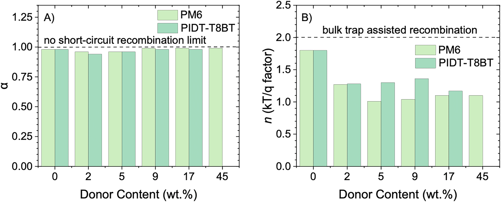 | ||
| Fig. 5 Electrical characterization of L8BO devices with varying donor content reveal that trap-assisted recombination is dominant for low donor devices. (A) Variation of the slope of JSCvs. lnI(α). (B) Variation of ideality factor n, determined from the slope of VOCvs. lnI. | ||
As a summary of TAS results, we see that pristine L8BO does not generate usable charges by itself when photoexcited. However, the interface it forms with the HTL generates charges. We note that these findings are in stark contrast to prior reports on Y6, claiming that substantial charges can be generated intrinsically in Y6 domains.40
Moreover, our results further demonstrate that while the charge generation does not critically depend upon the choice of the HTL, recombination does, as the energetic alignment of L8BO with the HTL plays a crucial role in the recombination of the generated charges. While charges generated in PEDOT/L8BO quickly recombine into triplets, the CuSCN/L8BO interface forms longer lasting charges. The addition of small quantities of polymer donor, enables to valorise the bulk of the PAL, due to charge generation at the donor:L8BO heterojunction, while in pristine L8BO, generation originates only from absorption in the vicinity of the HTL. Finally, charges generated by the HTL/PAL interface appear to decay faster than those generated in the bulk. Whether this is due to fast extraction or interface-induced recombination is studied using TPV and TPC.
Charge extraction and non-geminate recombination in L8BO devices
Notably, devices with L8BO as the PAL and CuSCN HTL demonstrated a reasonable FF of 61%. A slight drop was first observed in the FF with 2 wt% PM6, followed by a marginal increase upon adding 5 and 9 wt% PM6. The FF later showed a significant increase to 69% and 71% for 17 wt% and 45 wt% PM6, respectively. This suggests that even though the JSC was sharply increased in regime 1 (Fig. 2(C)) of the PM6 addition, different charge recombination mechanisms are likely at play when the donor content is systematically varied. To get further insights into the dominant recombination pathways, we first study the charge recombination in L8BO devices with varying amounts of donor polymer, by measuring the JSC and VOC as a function of the natural logarithm of light intensity (Fig. S19 and S20, ESI†).The dependence of the JSC on light intensity has been demonstrated to adhere to the relationship JSC ∝ Iα.41 In case of no non-geminate recombination at short circuit, α equals 1. Conversely, α < 1 indicates the presence of non-geminate recombination, and it has also been argued to originate due to an imbalance of hole and electron mobilities.42Fig. 5(A) shows the change in α as a function of varying amounts of polymer added to L8BO. Neat L8BO devices exhibited an α of 0.98, with no significant change observed upon the addition of PM6 and PIDT-T8BT (Fig. 5(A) and Table S3, ESI†). It is noteworthy that the variation of JSC with I primarily reflects the recombination of only the photogenerated carriers with each other. In contrast, the recombination of photogenerated charges with the dark carriers at the interface with transport layers dominates in OSCs.43,44 Therefore, a weak sublinear relationship between JSC and I might not provide conclusive evidence for bimolecular recombination quantitatively, particularly since most charges in L8BO devices with no donor content are created close to the interface, as seen by TAS measurements.
On the other hand, the VOCvs. ln(I) relationship has previously shown that different slopes convey distinct dominant loss mechanisms.41 An ideality factor n is determined from the slope of VOCvs. I plotted on a semilogarithmic scale using the relation:

The charge recombination and extraction mechanism in devices observed from steady-state measurements is further confirmed via transient photovoltage (TPV) and transient photocurrent (TPC) measurements on L8BO and polymer-L8BO BHJ devices (with varying amounts of PM6 and PIDT-T8BT) (Fig. S22 and Table S3, ESI†), using CuSCN as the HTL. The addition of donor polymer to L8BO devices resulted in faster extraction of photoinduced charges as evident from reduced extraction time from 0.82 μs for L8BO to less than 0.70 μs (Table S3, ESI†) when PM6 or PIDT-Y8BT are added to L8BO. Similarly, the addition of increasing amounts of PM6 to L8BO, significantly enhanced the carrier lifetime from 1.6 μs to 3.15 μs (Table S3, ESI†), in line with the UPS and TAS findings that the presence of donor favours the extraction of holes from L8BO to the HTL.
On the contrary, an increased amount of PIDT-T8BT is detrimental to both the extraction and recombination of photogenerated charge carriers, with carrier lifetime reducing from 1.6 μs to 0.9 μs when PIDT-T8BT content was increased up to 17 wt% (Fig. S22 and Table S3, ESI†). It could be hypothesized that due to the amorphous nature, PIDT-T8BT suffers from low mobility and high disorder, resulting in enhanced charge recombination.
It is noteworthy that the TPV carrier lifetime in the L8BO devices with small amounts of PM6 and a PEDOT:PSS HTL (Fig. S23, ESI†) were significantly lower than those for identical devices having a CuSCN HTL (Fig. S22, ESI†), also showing that the charges recombine relatively faster when PEDOT:PSS is used as the HTL as compared to CuSCN.
Electro-optical and drift-diffusion simulations
To theoretically substantiate the experimental findings, we employ electro-optical device simulations. Fig. 6(A) shows the calculated EQE of neat L8BO devices from optical simulations accounting for the diffusion of photogenerated excitons within the L8BO active layer. The photogeneration rate profile of excitons is calculated from an optical transfer-matrix model accounting for photon absorption and interference effects in the device stack.47,48 A diffusion length (LD) of 30 nm for excitons is assumed, similar to previous reports on L8BO and other Y6 series acceptors in the literature.19,49 | ||
| Fig. 6 Simulated photovoltaic properties of L8BO devices confirms that charge generation in pristine L8BO devices primarily happens close to the HTL-L8BO interface. (A) Simulated EQE in three different charge dissociation scenarios: at HTL only, at HTL and in the bulk, and the bulk. (B) The J–V curves of simulated and experimental L8BO devices with CuSCN HTL. (C) Simulated J–V curves with generation in different scenarios. (D) Simulated VOC dependence on light intensity. | ||
We find that the qualitative spectral features of the experimental EQE of neat L8BO can be reproduced if excitons are only allowed to dissociate at the HTL interface (Fig. 6(A)). In this case, excitons generated in the bulk L8BO must diffuse to the HTL interface to dissociate and generate charge carriers. Owing to the limited diffusion length, however, only excitons generated sufficiently close to the HTL (within a distance LD) can dissociate and contribute to the EQE. The corresponding EQE is dominated by a broad peak at wavelengths of 700–800 nm originating from photons absorbed near the HTL, while a smaller contribution is obtained from photons at wavelengths around 500 nm which are absorbed deeper in the bulk.
On the other hand, as shown in Fig. 6(A), by successively allowing for excitons to also dissociate in the L8BO bulk the contribution from excitons generated deeper in the bulk can be enhanced. Apart from increasing the overall EQE, this results in a relative increase of the peak at 500 nm, eventually becoming comparable to the peak at 700–800 nm. This is demonstrated in Fig. 6(A), which also includes the cases of partial and complete bulk dissociation.
These simulations support the above findings suggesting that exciton dissociation and charge carrier generation in pristine L8BO occurs primarily at the HTL interface, while the effect of adding trace amounts of donor is to introduce photocurrent generation in the L8BO bulk.
To further investigate the implications on device performance, we next turn to electrical drift-diffusion simulations.44 To this end, the neat L8BO device is treated as a bilayer HTL/L8BO cell where the generation and recombination of charge carriers occur at the HTL interface. As shown in Fig. 6(B), the experimental J–V characteristics of neat L8BO devices (symbols) can be reproduced by drift-diffusion simulations (solid lines) assuming the charge carrier recombination is dominated by traps at the HTL interface.
The effect of charge carrier generation in the bulk of L8BO is simulated in the lower panel of Fig. 6. The simulated J–V characteristics at 1 sun and light intensity dependence of the open-circuit voltage are shown in Fig. 6(C) and (D), respectively. As the charge carrier generation within the bulk is included and enhanced, the magnitude of the current is increased showing a similar trend to that obtained when adding small amounts of donor in the experiments. Simultaneously, the light ideality factor n decreases from 1.75 (no bulk generation) to 1.3 as the charge carrier generation within the bulk is enhanced. Again, this reproduces the experimental trend seen when adding small amounts of donor into the L8BO layer. The decreased light ideality factor is attributed to the reduced effect of trap-assisted recombination at the (trap-rich) HTL interface as more charge carriers are generated in the trap-free bulk where bimolecular recombination dominates.
Finally, we note that the observed behaviour of the PEDOT:PSS/L8BO device can be understood in terms of charge carrier generation at a highly defective HTL interface, virtually acting like a metal. This is demonstrated in Fig. S23 (ESI†) where the effect of increasing the trap density at the interface is simulated, suggesting that interface recombination is strongly enhanced with increasing trap density; at very high trap densities, the simulated J–V curve approaches the case with PEDOT:PSS as HTL. The subsequent low current levels obtained in this case are a direct consequence of charge carriers being exclusively generated at the HTL interface.
Conclusions
In conclusion, this study reveals that pristine NFA based devices function as a bilayer system, with charge generation taking place primarily at the HTL–PAL interface. Our findings underscore the pivotal role of HTL energetics in optimizing device performance. In devices with L8BO as the only PAL, CuSCN–L8BO interface proved more effective in generating and sustaining long-lived charges. In contrast, though the L8BO devices with PEDOT:PSS as the HTL also generate charges at the L8BO-PEDOT:PSS interface, these charges quickly recombine into L8BO triplet state excitons. The detrimental effect of PEDOT:PSS on charge recombination is attributed to significant interface recombination as a result of high trap-densities at the PEDOT:PSS–L8BO interface and highlights the importance of selecting charge transport materials with suitable energetics for achieving well-performing pristine NFA devices. Furthermore, the incorporation of a trace amount of donor polymer reduces the hole injection barrier at the HTL interface, and simultaneously enhancing the charge generation in the bulk of PAL. These insights contribute to a deeper understanding of NFA-only organic solar cells and pave the way for developing newer NFA designs with better intrinsic charge generation.Experimental
Materials
L8BO, PM6, and PNDIT-F3N were purchased from Solarmer Inc. PIDT-T8BT and PIDT-T12BT were synthesized according to previously reported procedures,30 and PIDT-T8BT has a![[M with combining macron]](https://www.rsc.org/images/entities/i_char_004d_0304.gif) n of 62.4 kg mol−1 and a ĐM of 2.59, while PIDT-T12BT has a n of 54.1 kg mol−1 and ĐM of 2.37. CuSCN, DES, Chloroform, MeOH and 1,8-diiiodooctane 98% were purchased from Sigma-Aldrich. All materials were used as received.
n of 62.4 kg mol−1 and a ĐM of 2.59, while PIDT-T12BT has a n of 54.1 kg mol−1 and ĐM of 2.37. CuSCN, DES, Chloroform, MeOH and 1,8-diiiodooctane 98% were purchased from Sigma-Aldrich. All materials were used as received.
Device fabrication and characterization
OSCs were fabricated with the ITO/CuSCN/PAL/PNDIT-F3N/Ag structure, else stated otherwise. ITO was cleaned using ultrasonication in water, acetone, and isopropanol for 10 minutes each, followed by 1 minute of microwave oxygen plasma. CuSCN was deposited from 26 mg mL−1 solution in DES at 2500 rpm, then thermally annealed at 105 deg. C for 10 minutes. All PALs were deposited in a nitrogen-filled glovebox from a 20 mg mL−1 solution in CHCL3 with 0.5% 1,8 diiodooctane (DIO). All L8BO and donor-L8BO PALs were thermally annealed at 100 °C for 1 minute. PNDIT-F3N was subsequently spin-coated from a 1.5 mg mL−1 solution in MeOH with 0.5% acetic acid at 1500 rpm. 100 nm of Ag was then thermally evaporated using a mask to define the geometric area of devices to be 0.1 cm−2. For all device fabrication and characterization, the wt% of donor polymers in L8BO has been approximated from their corresponding donor:acceptor (D:A) ratio in solution as follows: 0 wt% (0:1), 2 wt% (1:50), 5 wt% (1:20), 9 wt% (1:10), 17 wt% (1:5), 45 wt% (1:1.2).
For the J–V characterization of solar cells, at least six identical cells were measured for each type of device, by a Keithley 2400 source meter unit paired with PV Measurement Inc. solar simulator fitted with a xenon light source, calibrated to give AM1.5G simulated spectrum with intensity equal to 1 sun. For pristine L8BO PAL devices on CuSCN, over 20 devices prepared across different batches were measured to determine average PCE values (Table S1, ESI†). LabVIEW program was used to acquire and process the J–V data. J–V curves were plotted only in forward directions (at a scan speed of 0.02 or 0.05 V step−1 and swell time of 20 ms), as no hysteresis was observed. All devices were electrically tested in a N2 filled glovebox at room temperature, with no anti-reflecting coating.
Transient photovoltage (TPV) and transient photocurrent (TPC) measurements
To examine the charge recombination and extraction processes in the devices, TPV and TPC measurements were performed using the integrated PAIOS 3.2 platform system (Fluxim). A calibrated white LED with a rise/fall time of 100 ns served as the light source, controlled by one function generator for the light modulation and a second function generator for the bias application. The resulting current was then recorded using a transimpedance amplifier.Transient absorption spectroscopy (TAS)
TA spectroscopy was carried out using a custom pump–probe setup. The output of a titanium:sapphire amplifier (Coherent LEGEND DUO, 4.5 mJ, 3 kHz, 100 fs) was split into three beams (2, 1, and 1.5 mJ). One of them was used to produce a white-light supercontinuum from 550 to 1700 nm by sending the 800 nm pulses through a sapphire (3 mm thick) crystal. One of the other beams was used to separately pump an optical parametric amplifiers (OPA) (light conversion TOPAS prime). The pump–probe delay was adjusted by reducing the probe beam pathway between 5.12 and 2.6 m while the pump pathway length to the sample was kept constant at ∼5 m between the output of TOPAS 1 and the sample. The pump–probe path length was varied with a broadband retroreflector mounted on an automated mechanical delay stage (broadband Newport retroreflector mounted on a Thorlabs linear stage ODL600/M controlled by a Thorlabs BBD301 motion controller), thereby generating delays between pump and probe from −40 ps to 8 ns.An actively Q-switched Nd:YVO4 laser (InnoLas picolo AOT) provided the excitation light (532 nm) for long delay (1 ns–300 μs) TA experiments which is triggered by an electronic delay generator (Stanford Research Systems DG535). The electronic delay generator triggered by the TTL sync from the Legend DUO, allows to control of the delay between pump and probe with a jitter of roughly 100 ps.
The samples were kept under vacuum (below 10−6 mbar) during the entire measurements. The transmitted fraction of the white light was guided to a custom-made prism spectrograph (Entwicklungsbüro Stresing) where it was dispersed by a prism onto a 512 pixels complementary metal-oxide semiconductor (CMOS) linear image sensor (Hamamatsu G11608-512DA) for broadband (550–1700 nm) detection. The probe pulse repetition rate was 3 kHz, while the excitation pulses were directly generated at 1.5 kHz frequency (ns–μs delays) or mechanically chopped down from 3 kHz to 1.5 kHz (ps–ns delays), and the detector array was read out at 3 kHz. Adjacent diode readings corresponding to the transmission of the sample after excitation and in the absence of an excitation pulse, respectively, were used to calculate ΔT/T. Measurements were averaged over several thousand shots to obtain a good signal-to noise ratio. The chirp induced by the transmissive optics was corrected with a custom Matlab script. The delay at which pump and probe arrive simultaneously on the sample (i.e., zero time) was determined from the point of the maximum positive slope of the TA signal rise for each wavelength.
TDCF measurements
The TDCF system, which was custom-built, employs the second harmonic wavelength (532 nm) from an actively Q-switched sub-ns Nd:YVO4 laser (INNOLAS Picolo AOT) operating at 5 kHz for excitation. To reduce the resistance–capacitance (RC) response time, which is usually a few nanoseconds, a device with a small area of 1 mm2 was utilized. Measurements were conducted under dynamic vacuum conditions to prevent sample degradation. The pre-bias and extraction bias were supplied by a Keysight S1160A functional generator, and the current response of the device was recorded using a four-channel digital oscilloscope from Keysight.Ultraviolet photoelectron spectroscopy (UPS) and low-energy inverse photoelectron spectroscopy (LE-IPES)
UPS measurements were conducted within an ultrahigh vacuum chamber (base pressure of 10−10 mbar) using an ARGUS-CU analyser equipped with a 128 channel stripped anode detector (ScientaOmicron) calibrated against the Fermi edge of clean polycrystalline silver. The analysis employed a low-intensity UV light source (He I) with an excitation energy of 21.22 eV and a pass energy of 3 eV.LE-IPES measurements were performed in isochromatic mode utilizing an ultra-high vacuum setup, operational at a base pressure of 10−9 mbar. Photons emitted were captured using a solid-state photomultiplier tube (PMT) detector (Hamamatsu R585), positioned external to the vacuum. This detector was equipped with a Semrock 280 nm bandpass filter, which allowed a narrow wavelength window of 10 nm, and an integration time of maximum 15 s. To ensure the integrity of the spectral data, samples were swiftly transferred from the UPS to the LE-IPES manipulator within the controlled ultra-high vacuum environment, thus avoiding any contamination through air exposure.
For these measurements, we cast thin films of L8BO and L8BO-polymer BHJ blend on Au-coated Si wafers with a 10 nm layer of sputtered titanium to improve the Au adhesion. For BHJ films, a 10 wt% donor was used for UPS and IPES measurements. This is to have a comparable distribution of donor and acceptor content on the surface of the studied films while avoiding surface saturation of BHJ film with the polymer, which is often the case with D/A ratio of 1:1 due to lower surface energy of the polymer. BHJ films were deposited on CuSCN-coated ITO, to mimic the device stack.
Sensitive external quantum efficiency (sEQE) measurements
A Xenon source (Newport 300 W ozone-free xenon arc lamp) with a monochromator (QD Lot, MSH-300) is used to produce mechanically chopped (Stanford Research Systems SR540 optical chopper) monochromatic light at 473 Hz. An optical fiber is used to bring the light beam into the glove box and an optical assembly composed of filters and focusing lenses are used to adjust the spot size of the beam. A current pre-amplifier (Standford Research Systems 530) and a lock-in amplifier (Stanford Research Systems SR830 lock-in amplifier) are used to attain a high level of sensitivity. The automatic measurement routine is performed by a home-built LabVIEW program. For the calibration, a Silicon and Germanium Detector (Newport 71619) were used.Electroluminescence (EL) measurements
A Keithley 2400 source meter was used to apply a constant current to the devices. An optical fibre was placed immediately behind the transparent electrode to bring the signal from the device to the spectrograph (Princeton instruments).Absolute electroluminescence measurements (EQEEL)
A Keithley 2400 source meter was used to apply a constant current to the devices. A calibrated Si photodetector (Thorlabs FDS1010-CAL) was placed behind the transparent electrode, and a precision source meter (Keysight 82902A) was used to record the current from the Si photodetector.Equations used to calculate the energy losses.
The VOC is calculated from the Shockley–Quisser limit:

Assuming all recombination is radiative, the radiative VOC limit is given by:

The total energy loss can be given as:
| Eloss = ΔE1 + ΔE2 + ΔE3 |
The radiative recombination loss above the band gap, ΔE1, is calculated from:
| ΔE1 = Eg − qVSQOC |
The radiative recombination loss below the gap, ΔE2, is calculated from:
| ΔE2 = qVSQOC − qVradOC |
The non-radiative recombination loss, ΔE3, is calculated from:
| Eg − qVOC = ΔE1 + ΔE2 + ΔE3 |
Alternatively, ΔE3, can also be calculated from the EQEEL as follows:
| qΔE3 = −kTln(EQEEL) |
Author contributions
A. S.: conceptualization, investigation, data curation, project administration, writing – original draft. A. S. conducted the research. A. S. and H. X. fabricated and characterized the devices. J. B. assisted in device fabrication. J. G. performed TAS measurements, writing – review and editing. J. P. J. performed sEQE and EL measurements. S. A. performed TDCF measurements. D. R. V. performed GIWAXS measurements. X. P. synthesized PIDT-T8BT and PIDT-T12BT polymers. P. D. N. performed spectroelectrochemistry measurements on PEDOT:PBS films. O. J. S. performed electro-optical and drift-diffusion simulations. Y. H. and Y. L. helped with TAS measurements. M. A. helped with EL measurements. M. R. A, F. L., and D. B.: writing – review and editing; D. B.: resources, supervision. All authors approved the final version of the manuscript.Conflicts of interest
There are no conflicts to declare.Data availability
The data supporting this article have been included as part of the ESI.†Acknowledgements
This work was supported by King Abdullah University of Science and Technology (KAUST) Office of Sponsored Research (OSR) under award no: OSR-CARF/CCF-3079 and ORA-CRG10-2021-4681. The authors greatly acknowledge the device fabrication and characterization facilities at the KAUST Solar Center. O. J. S. acknowledges funding from the Research Council of Finland through project no. 357196. Y. H. thanks the research grant from KAUST global postdoc fellowship (award No. ORA-2023-6014).References
- H. Chen, Y. Huang, R. Zhang, H. Mou, J. Ding, J. Zhou, Z. Wang, H. Li, W. Chen, J. Zhu, Q. Cheng, H. Gu, X. Wu, T. Zhang, Y. Wang, H. Zhu, Z. Xie, F. Gao, Y. Li and Y. Li, Nat. Mater., 2025, 24, 444–453 CrossRef CAS PubMed.
- Y. Cai, Y. Li, R. Wang, H. Wu, Z. Chen, J. Zhang, Z. Ma, X. Hao, Y. Zhao, C. Zhang, F. Huang and Y. Sun, Adv. Mater., 2021, 33, 2101733 CrossRef CAS PubMed.
- Y. Firdaus, V. M. Le Corre, S. Karuthedath, W. Liu, A. Markina, W. Huang, S. Chattopadhyay, M. M. Nahid, M. I. Nugraha, Y. Lin, A. Seitkhan, A. Basu, W. Zhang, I. McCulloch, H. Ade, J. Labram, F. Laquai, D. Andrienko, L. J. A. Koster and T. D. Anthopoulos, Nat. Commun., 2020, 11, 5220 CrossRef CAS PubMed.
- J. Bertrandie, J. Han, C. S. P. De Castro, E. Yengel, J. Gorenflot, T. Anthopoulos, F. Laquai, A. Sharma and D. Baran, Adv. Mater., 2022, 34, e2202575 CrossRef PubMed.
- S. Karuthedath, J. Gorenflot, Y. Firdaus, N. Chaturvedi, C. S. P. De Castro, G. T. Harrison, J. I. Khan, A. Markina, A. H. Balawi, T. A. D. Peña, W. Liu, R.-Z. Liang, A. Sharma, S. H. K. Paleti, W. Zhang, Y. Lin, E. Alarousu, D. H. Anjum, P. M. Beaujuge, S. De Wolf, I. McCulloch, T. D. Anthopoulos, D. Baran, D. Andrienko and F. Laquai, Nat. Mater., 2021, 20, 378–384 CrossRef CAS PubMed.
- X. K. Chen, D. P. Qian, Y. M. Wang, T. Kirchartz, W. Tress, H. F. Yao, J. Yuan, M. Hulsbeck, M. J. Zhang, Y. P. Zou, Y. M. Sun, Y. F. Li, J. H. Hou, O. Inganas, V. Coropceanu, J. L. Bredas and F. Gao, Nat. Energy, 2021, 6, 799–806 CrossRef CAS.
- A. Markina, K.-H. Lin, W. Liu, C. Poelking, Y. Firdaus, D. R. Villalva, J. I. Khan, S. H. K. Paleti, G. T. Harrison, J. Gorenflot, W. Zhang, S. De Wolf, I. McCulloch, T. D. Anthopoulos, D. Baran, F. Laquai and D. Andrienko, Adv. Energy Mater., 2021, 11, 2102363 CrossRef CAS.
- M. B. Price, P. A. Hume, A. Ilina, I. Wagner, R. R. Tamming, K. E. Thorn, W. Jiao, A. Goldingay, P. J. Conaghan, G. Lakhwani, N. J. L. K. Davis, Y. Wang, P. Xue, H. Lu, K. Chen, X. Zhan and J. M. Hodgkiss, Nat. Commun., 2022, 13, 2827 CrossRef CAS PubMed.
- E. Saglamkaya, A. Musiienko, M. S. Shadabroo, B. Sun, S. Chandrabose, O. Shargaieva, M. G. Lo Gerfo, N. F. van Hulst and S. Shoaee, Mater. Horiz., 2023, 10, 1825–1834 RSC.
- A. Sharma, N. Gasparini, A. Markina, S. Karuthedath, J. Gorenflot, H. Xu, J. Han, A. Balawi, W. Liu, D. Bryant, J. Bertrandie, J. Troughton, S. H. K. Paleti, H. Bristow, F. Laquai, D. Andrienko and D. Baran, Adv. Mater., 2024, 36, 2305367 CrossRef CAS PubMed.
- Y. Fu, T. H. Lee, Y.-C. Chin, R. A. Pacalaj, C. Labanti, S. Y. Park, Y. Dong, H. W. Cho, J. Y. Kim, D. Minami, J. R. Durrant and J.-S. Kim, Nat. Commun., 2023, 14, 1870 CrossRef CAS PubMed.
- A. Dolan, X. Pan, M. J. Griffith, A. Sharma, J. M. de la Perrelle, D. Baran, G. F. Metha, D. M. Huang, T. W. Kee and M. R. Andersson, Adv. Mater., 2024, 36, 2309672 CrossRef CAS PubMed.
- F. Eisner, G. Foot, J. Yan, M. Azzouzi, D. G. Georgiadou, W. Y. Sit, Y. Firdaus, G. Zhang, Y.-H. Lin, H.-L. Yip, T. D. Anthopoulos and J. Nelson, Adv. Mater., 2022, 34, 2104654 CrossRef CAS PubMed.
- A. Sharma, S. Singh, X. Song, D. Rosas Villalva, J. Troughton, D. Corzo, L. Toppare, G. Gunbas, B. C. Schroeder and D. Baran, Chem. Mater., 2021, 33, 8602–8611 CrossRef CAS PubMed.
- J. M. Bjuggren, A. Sharma, D. Gedefaw, S. Elmas, C. Pan, B. Kirk, X. Zhao, G. Andersson and M. R. Andersson, ACS Appl. Energy Mater., 2018, 1, 7130–7139 CrossRef CAS.
- Z. Zhang, L. Li, C. Xu, P. Jin, M. Huang, Y. Li, H. Wang, Y. Yi, C. Zhang, Y. Yang, W. Xu and Y. Lin, Cell Rep. Phys. Sci., 2022, 3, 100895 CrossRef CAS.
- G. Zhou, M. Zhang, J. Xu, Y. Yang, T. Hao, L. Zhu, L. Zhou, H. Zhu, Y. Zou, G. Wei, Y. Zhang and F. Liu, Energy Environ. Sci., 2022, 15, 3483–3493 RSC.
- C. Li, J. Zhou, J. Song, J. Xu, H. Zhang, X. Zhang, J. Guo, L. Zhu, D. Wei, G. Han, J. Min, Y. Zhang, Z. Xie, Y. Yi, H. Yan, F. Gao, F. Liu and Y. Sun, Nat. Energy, 2021, 6, 605–613 CrossRef CAS.
- L. Zhu, M. Zhang, J. Xu, C. Li, J. Yan, G. Zhou, W. Zhong, T. Hao, J. Song, X. Xue, Z. Zhou, R. Zeng, H. Zhu, C.-C. Chen, R. C. I. MacKenzie, Y. Zou, J. Nelson, Y. Zhang, Y. Sun and F. Liu, Nat. Mater., 2022, 21, 656–663 CrossRef CAS PubMed.
- H. Xu, A. Sharma, J. H. Han, B. P. Kirk, A. R. Alghamdi, F. Z. Xu, Y. C. Zhang, A. H. Emwas, G. Hizalan, S. De Wolf, M. R. Andersson, G. G. Andersson and D. Baran, Adv. Energy Mater., 2024, 14, 2401262 CrossRef CAS.
- X. e Li, Q. Zhang, J. Yu, Y. Xu, R. Zhang, C. Wang, H. Zhang, S. Fabiano, X. Liu, J. Hou, F. Gao and M. Fahlman, Nat. Commun., 2022, 13, 2046 CrossRef CAS PubMed.
- M. Kim, S. Park, J. Jeong, D. Shin, J. Kim, S. H. Ryu, K. S. Kim, H. Lee and Y. Yi, J. Phys. Chem. Lett., 2016, 7, 2856–2861 CrossRef CAS PubMed.
- P. Pattanasattayavong, V. Promarak and T. D. Anthopoulos, Adv. Electron. Mater., 2017, 3, 1600378 CrossRef.
- G. Greczynski, T. Kugler, M. Keil, W. Osikowicz, M. Fahlman and W. R. Salaneck, J. Electron Spectrosc. Relat. Phenom., 2001, 121, 1–17 CrossRef CAS.
- V. Belova, A. Perevedentsev, J. Gorenflot, C. S. P. De Castro, M. Casademont-Viñas, S. H. K. Paleti, S. Karuthedath, D. Baran, F. Laquai and M. Campoy-Quiles, Solar RRL, 2022, 6, 2100822 CrossRef CAS.
- D. Qian, Z. Zheng, H. Yao, W. Tress, T. R. Hopper, S. Chen, S. Li, J. Liu, S. Chen, J. Zhang, X. K. Liu, B. Gao, L. Ouyang, Y. Jin, G. Pozina, I. A. Buyanova, W. M. Chen, O. Inganas, V. Coropceanu, J. L. Bredas, H. Yan, J. Hou, F. Zhang, A. A. Bakulin and F. Gao, Nat. Mater., 2018, 17, 703–709 CrossRef CAS PubMed.
- U. Rau, Phys. Rev. B: Condens. Matter Mater. Phys., 2007, 76, 085303 CrossRef.
- J. Kern, S. Schwab, C. Deibel and V. Dyakonov, Phys. Status Solidi RRL, 2011, 5, 364–366 CrossRef CAS.
- N. Schopp, G. Akhtanova, P. Panoy, A. Arbuz, S. Chae, A. Yi, H. J. Kim, V. Promarak, T.-Q. Nguyen and V. V. Brus, Adv. Mater., 2022, 34, 2203796 CrossRef CAS PubMed.
- X. Pan, J. M. Bjuggren, M. Jevric, W. L. Tan, C. R. McNeill and M. R. Andersson, Chem. Mater., 2022, 34, 5103–5115 CrossRef CAS.
- X. Huang, X. Liu, K. Ding and S. R. Forrest, Materials Horizons, 2020, 7, 244–251 RSC.
- Y. Nakayama, S. Kera and N. Ueno, J. Mater. Chem. C, 2020, 8, 9090–9132 RSC.
- M. Schwarze, W. Tress, B. Beyer, F. Gao, R. Scholz, C. Poelking, K. Ortstein, A. A. Günther, D. Kasemann, D. Andrienko and K. Leo, Science, 2016, 352, 1446–1449 CrossRef CAS PubMed.
- Z. He, S. Li, R. Zeng, Y. Lin, Y. Zhang, Z. Hao, S. Zhang, F. Liu, Z. Tang and H. Zhong, Adv. Mater., 2024, 36, 2404824 CrossRef CAS PubMed.
- O. L. Gribkova, O. D. Iakobson, A. A. Nekrasov, V. A. Cabanova, V. A. Tverskoy and A. V. Vannikov, J. Solid State Electrochem., 2016, 20, 2991–3001 CrossRef CAS.
- S. Giannini, D. J. C. Sowood, J. Cerdá, S. Frederix, J. Grüne, G. Londi, T. Marsh, P. Ghosh, I. Duchemin, N. C. Greenham, K. Vandewal, G. D’Avino, A. J. Gillett and D. Beljonne, Mater. Today, 2024, 80, 308–326 CrossRef CAS.
- P. A. Hume, M. B. Price and J. M. Hodgkiss, JACS Au, 2024, 4, 1295–1302 CrossRef CAS PubMed.
- R. Wang, C. Zhang, Q. Li, Z. Zhang, X. Wang and M. Xiao, J. Am. Chem. Soc., 2020, 142, 12751–12759 CrossRef CAS PubMed.
- S. Karuthedath, J. Gorenflot, A. Melianas, Z. Kan, M. Kemerink and F. Laquai, J. Phys. Chem. Lett., 2020, 11, 2838–2845 CrossRef CAS PubMed.
- Y. Wang, M. B. Price, R. S. Bobba, H. Lu, J. Xue, Y. Wang, M. Li, A. Ilina, P. A. Hume, B. Jia, T. Li, Y. Zhang, N. Davis, Z. Tang, W. Ma, Q. Qiao, J. M. Hodgkiss and X. Zhan, Adv. Mater., 2022, 34, 2206717 CrossRef CAS PubMed.
- P. Schilinsky, C. Waldauf and C. J. Brabec, Appl. Phys. Lett., 2002, 81, 3885–3887 CrossRef CAS.
- L. J. A. Koster, V. D. Mihailetchi, H. Xie and P. W. M. Blom, Appl. Phys. Lett., 2005, 87, 203502 CrossRef.
- U. Würfel, L. Perdigón-Toro, J. Kurpiers, C. M. Wolff, P. Caprioglio, J. J. Rech, J. Zhu, X. Zhan, W. You, S. Shoaee, D. Neher and M. Stolterfoht, J. Phys. Chem. Lett., 2019, 10, 3473–3480 CrossRef PubMed.
- O. J. Sandberg and A. Armin, PRX Energy, 2024, 3, 023008 CrossRef.
- V. V. Brus, Org. Electron., 2016, 29, 1–6 CrossRef CAS.
- G. Akhtanova, H. P. Parkhomenko, J. Vollbrecht, A. I. Mostovyi, N. Schopp and V. Brus, Org. Electron., 2025, 137, 107183 CrossRef CAS.
- L. A. A. Pettersson, L. S. Roman and O. Inganäs, J. Appl. Phys., 1999, 86, 487–496 CrossRef CAS.
- G. F. Burkhard, E. T. Hoke and M. D. McGehee, Adv. Mater., 2010, 22, 3293–3297 CrossRef CAS PubMed.
- D. B. Riley, O. J. Sandberg, W. Li, P. Meredith and A. Armin, Phys. Rev. Appl., 2022, 17, 024076 CrossRef CAS.
Footnotes |
| † Electronic supplementary information (ESI) available. See DOI: https://doi.org/10.1039/d5ee02324f |
| ‡ Present address: Physical Chemistry and Spectroscopy of Energy Materials, Department of Chemistry, Ludwig Maximilian University of Munich, D-81377 Munich, Germany. |
| This journal is © The Royal Society of Chemistry 2025 |