
 Open Access Article
 This Open Access Article is licensed under a Creative Commons Attribution-Non Commercial 3.0 Unported Licence
Conversion of photovoltaic waste silicon into amorphous silicon nanowire anodes†
Liao
Shen‡
a,
Kaiwen
Sun‡
 c,
Fengshuo
Xi‡
a,
Zhitao
Jiang
a,
Shaoyuan
Li
*a,
Yanfeng
Wang
a,
Zhongqiu
Tong
a,
Jijun
Lu
*a,
Wenhui
Ma
*ab,
Martin A.
Green
c and
Xiaojing
Hao
*c
c,
Fengshuo
Xi‡
a,
Zhitao
Jiang
a,
Shaoyuan
Li
*a,
Yanfeng
Wang
a,
Zhongqiu
Tong
a,
Jijun
Lu
*a,
Wenhui
Ma
*ab,
Martin A.
Green
c and
Xiaojing
Hao
*c
aFaculty of Metallurgical and Energy Engineering, Key Laboratory of Complex Nonferrous Metal Resources Clean Utilization, Kunming University of Science and Technology, Kunming, 650093, China. E-mail: lsysilicon@kust.edu.cn; jjlu@kust.edu.cn
bSchool of Engineering, Yunnan University, Kunming, 650500, China. E-mail: mawenhui@ynu.edu.cn
cAustralian Centre for Advanced Photovoltaics, School of Photovoltaic and Renewable Energy Engineering, University of New South Wales, Sydney, NSW 2052, Australia. E-mail: xj.hao@unsw.edu.au
First published on 7th April 2025
Abstract
The rapid growth of the crystalline silicon (Si) photovoltaic industry has led to a steady increase in the production of waste silicon (wSi) generated during the cutting of Si ingots. Nevertheless, intrinsic oxidation and trace impurities in wSi make it difficult to retain or enhance its value for further use. Herein, we proposed a value-added recycling strategy to flash convert wSi into high performance amorphous Si nanowires (a-SiNWs). This method fully leverages the intrinsic oxidation properties of wSi and utilizes a high temperature gradient thermal field generated by carbon thermal shock to drive the directional diffusion of Si atoms within an oxide-limited domain environment. Copper nanoparticles are introduced to modulate the surface energy of Si atoms, inducing the formation of a-SiNWs. The a-SiNWs grow in situ on a carbon substrate, forming a self-supporting electrode material (identified as a-SiNWs@CC). The prepared a-SiNWs@CC is directly used as the anode of lithium-ion batteries, demonstrating excellent initial coulombic efficiency (ICE, 91.35%) and lithium storage capacity (up to 2150 mA h g−1 at 2 A g−1 for more than 250 cycles). The results hold great promise for the high-value utilization of wSi and the development of Si anodes.
Broader contextThe sustainable development of crystalline silicon (c-Si) photovoltaic solar power generation and silicon-based energy storage is expected to promote the integration of the “photovoltaic-storage” industry chain. However, in the photovoltaic industry, nearly 40% of c-Si is converted into waste silicon (wSi) during the cutting process. Currently, most wSi is managed through landfill disposal or remelting and refining, yielding limited results in the photovoltaic and energy storage fields and making upcycling difficult to achieve. In this work, we utilize the intrinsic oxidation properties of wSi and the high-temperature gradient thermal field provided by carbothermal shock to drive the directional diffusion of Si atoms within confined oxide spaces, enabling the rapid conversion of wSi into amorphous silicon nanowires (a-SiNWs). It is further clarified that the induction by Cu is critical for the formation of the a-SiNWs, as it reduces the surface energy on the Si and accelerates the precipitation of Si atoms. And the amorphous structure facilitates electron/ion transport, enhancing the cycling and rate performance of lithium-ion batteries. This work provides valuable guidance for the high-value utilization of secondary resources and the structural design of silicon-based materials. |
Introduction
In recent decades, renewable energy has shown a continuous expansion trend. The development of the photovoltaic industry has driven the growth rate of crystalline silicon (c-Si) to exceed 30%, capturing 95% of the market share in the industry.1,2 The manufacturing process of c-Si wafers generates a large amount of low-purity and low-value cutting waste silicon (wSi). This waste exceeds 200![[thin space (1/6-em)]](https://www.rsc.org/images/entities/char_2009.gif) 000 tons annually, leading to a direct economic loss of approximately $300 million.3–5 Such a significant volume of wSi poses serious environmental and economic challenges to society. Unfortunately, regarding the utilization of wSi, these wastes have so far been processed into secondary resources such as silicon–aluminum alloys6 or silicon–carbon ceramics7 or re-melted and refined to return as high-purity Si raw materials for photovoltaics.8 Complex recycling technologies result in significant energy consumption and environmental re-pollution, leaving wSi in a state of idleness or low value utilization. Therefore, finding high value utilization pathways for wSi is of great importance.
000 tons annually, leading to a direct economic loss of approximately $300 million.3–5 Such a significant volume of wSi poses serious environmental and economic challenges to society. Unfortunately, regarding the utilization of wSi, these wastes have so far been processed into secondary resources such as silicon–aluminum alloys6 or silicon–carbon ceramics7 or re-melted and refined to return as high-purity Si raw materials for photovoltaics.8 Complex recycling technologies result in significant energy consumption and environmental re-pollution, leaving wSi in a state of idleness or low value utilization. Therefore, finding high value utilization pathways for wSi is of great importance.
In fact, lithium storage technology imposes relatively lenient restrictions on the purity and defects of Si, as it primarily relies on the reversible migration of lithium ions between the cathode and the anode.9 Moreover, Si possesses an extremely ultra-high theoretical capacity (4200 mA h g−1) and a safe lithiation potential (<0.4 V vs. Li/Li+).10,11 Therefore, using wSi to manufacture silicon-based anodes has garnered considerable attention in both academic and industrial research studies.12,13 However, making Si anodes from wSi faces critical challenges. In addition to the significant volume expansion effect (>300%) during (de)lithiation and its poor conductivity, wSi also suffers from severe surface oxidation and an inconsistent particle size distribution.14 To address these issues, various strategies have been developed, such as mechanical grinding,15 doping,16 graphite/carbon composites,17 chemical etching,18 and metal oxide coatings.19 Nevertheless, these strategies generally involve complex and lengthy preparation processes without altering the intrinsic properties of wSi. As a result, the electrochemical performance has not shown significant improvement.
Nowadays, the structural design of one-dimensional nanowires is considered a promising solution to the issues of silicon-based anodes, as they can accommodate large strains and offer rapid electron/ion transport rates.20,21 Additionally, compared to c-Si, amorphous Si (a-Si) is favored for its isotropic structure, which can better accommodate volume changes during the charge/discharge processes.22–24 Therefore, converting wSi into a-Si nanowire (a-SiNWs) structures is an effective strategy to mitigate the collapse during the repeated (de)lithiation process, thereby enhancing its lithium storage. However, in traditional fabrication processes, such as metal-assisted chemical etching,25 vapor deposition,26 and molten salt electrolysis,27 the resulting nanowires are mostly crystalline and rely on noble metal catalysts (e.g., Au and In) to induce growth. Additionally, the slow heating and cooling rates (<100 K s−1) lead to atomic or molecular rearrangement processes that are constrained by thermodynamic and kinetic factors, making it difficult to directly convert wSi into a nanowire.28 Thus, overcoming the limitations of traditional processes and accelerating the precipitation of Si atoms to synthesize a-SiNWs is both urgent and challenging.
In this work, we report a strategy for the instantaneous structural conversion of photovoltaic wSi into a-SiNWs. Utilizing the high-gradient thermal field generated by carbon thermal shock (CTS, ca. 4.2 × 10³ K s−1, temperature 2100 K, duration 0.5 s), the limitations of traditional heating and cooling rates can be overcome, allowing the wSi powder to rapidly liquefy and fission. With the decomposition of copper (Cu) salts, a Si–Cu melt can be formed. The introduction of Cu reduces the surface energy of Si particles and accelerates the directional diffusion of Si atoms under oxygen-limited domain conditions, promoting the in situ growth of a-SiNWs on the carbon cloth. Ultimately, a high-performance self-supporting anode (denoted as a-SiNWs@CC) is achieved for lithium-ion batteries, with an initial coulombic efficiency (ICE) of 91.35% at 0.2 A g−1. After 250 cycles at 2.0 A g−1, the capacity remains 2150 mA h g−1, maintaining a retention rate of 90% at the same current.
Results and discussion
Synthesis and structural characterization
The intrinsic properties of wSi and the transient high-temperature decomposition of metal Cu salts were studied in detail through characterization and experiments. Inductively coupled plasma (ICP) tests indicate that the impurity content in wSi is relatively low, mainly consisting of iron, aluminum, nickel, and copper (Table S1, ESI†). A laser particle size analyzer and a SEM revealed that the wSi has a particle size distribution with a D50 of approximately 380 nm (Fig. S1, ESI†), presenting irregular clastic particles. Further characterization using transmission electron microscopy (TEM) and X-ray photoelectron spectroscopy (XPS) in Fig. S2 (ESI†) showed that the wSi mainly consists of c-Si with an amorphous oxide layer on the surface. The presence of such an oxide layer is also suggested by the Si 2p spectrum. Fig. S3 (ESI†) shows the CTS technique device and its structural diagram, which is capable of providing ultrafast heating and quenching. Table S2 and Fig. S4 (ESI†) present the physical properties and Raman spectra of carbon cloth. Its excellent electrical conductivity is crucial for heat generation under high current, and the presence of defects offers favorable sites for the growth of nanowires.To verify the feasibility of introducing Cu particles, the carbon cloth loaded with Cu salts underwent CTS treatment. The results showed the presence of distinct fine metallic particles on the carbon cloth (Fig. S5 and S6 ESI†). As illustrated in Fig. S7 (ESI†), under a slightly reductive atmosphere (an Ar atmosphere containing 5 wt% H2) and a carbon substrate, the metal salts rapidly decompose, liquefy, and split into nanoparticles at instantaneous high temperatures. This high-temperature decomposition behavior provides strong evidence for the formation of metallic particles.
Fig. 1a illustrates the process flow of mixing Cu salts with wSi followed by CTS treatment. The carbon cloth substrate with a loaded mixture is connected to the power supply at both ends, where a pulsed current is applied to achieve transient heating and quenching. Temperature is determined using an infrared high temperature sensor (as shown in Fig. 1b, temperature ∼2100 K, heating rate 4.2 × 10³ K s−1). Under the influence of a large temperature gradient in the thermal field, the wSi is ultimately converted into a-SiNWs.
 | ||
| Fig. 1 The CTS process for synthesizing a-SiNWs@CC. (a) Schematic diagram and (b) temperature profile and optical images of the carbon cloth substrate at different stages. | ||
The morphological and structural analyses of the material were conducted using both scanning electron microscope (SEM) and TEM. Fig. 2a illustrates the growth process of the a-SiNWs. Specifically, Fig. 2b shows the SEM image of the carbon cloth, whose appropriate surface area provides excellent attachment points for the mixture. The carbon cloth loaded with the wSi and Cu salt mixture (Fig. 2c and d and Fig. S8, ESI†) underwent CTS treatment under different conditions. The results show that, as illustrated in Fig. S9 (ESI†), at around 1655 K, the nanowires are short and dense, while at 2368 K, they become longer and more sparsely distributed. Notably, at approximately 2100 K, the prepared a-SiNWs@CC exhibited a relatively uniform linear morphology (Fig. 2e–g) and had an optimized loading mass (2.0 mg cm−2, Table S3, ESI†). These results can provide valuable guidance for the morphology and growth regulation of Si nanowires.
 | ||
| Fig. 2 The morphological and structural characterization. (a) Growth diagram, (b) pristine carbon cloth, (c) and (d) SEM images at different magnifications of the carbon cloth surface with the loaded wSi and Cu salt mixture, (e)–(g) microscopic morphology of a-SiNWs@CC at different magnifications, and (h) and (i) TEM and HRTEM images, (j) SAED pattern, and (k) HAADF and EDS elemental mapping of the a-SiNWs. | ||
As shown in Fig. 2g and Fig. S10 (ESI†), the Si nanowires generated a-SiNWs@CC have a diameter of approximately 15 nm and exhibit a high length–diameter ratio, and the spherical cap at the top of the nanowires is slightly thicker than the wires. Furthermore, as shown in Fig. 2h and i, the TEM and high-resolution TEM (HRTEM) images reveal that the a-SiNWs@CC has an amorphous structure. The spherical cap at the tip of the nanowire shows varying contrast, and a lattice spacing of 0.20 nm in HRTEM corresponds to the (111) plane of Cu (Fig. 2i).29 The selected area electron diffraction (SAED) pattern in Fig. 2j further confirms the amorphous structure of the nanowires. High-angle annular dark field (HAADF) imaging and energy dispersive spectroscopy (EDS) elemental mapping (Fig. 2k) reveal that the nanowires are primarily composed of Si and O, with Cu clearly visible at their tips. The mass ratio of Si and O elements (Table S4, ESI†) further suggests that a-SiNWs@CC is predominantly Si, with a small amount of oxidation due to the inherent oxidation layer of the wSi.
However, for the sample c-SiNWs@CC without the Cu salt, although its morphology is similar to that of a-SiNWs@CC (Fig. S11, ESI†), TEM imaging (Fig. S12, ESI†) reveals distinct lattice fringes within the linear portions of c-SiNWs@CC, with lattice spacings corresponding to the (111) planes of crystalline Si, indicating the growth of crystalline Si nanowires (c-SiNWs).30 Combined with EDS elemental mapping and the silicon-to-oxygen mass ratio (Fig. S12 and Table S4, ESI†), an oxidation layer of approximately 5 nm thick is observed at the edges, which limits the growth of nanowires in non-one-dimensional directions.
To accurately understand the growth mechanism of a-SiNWs@CC, the standard Gibbs free energy changes (ΔrGθm) for Si-related chemical reactions during the CTS process were calculated. As shown in Fig. S13 (ESI†), the results indicate that, in a system containing Si, silica, and carbon (with silica derived from the oxidation of wSi), the formation of gaseous SiO proceeds favorably at around 2100 K. This promotes melt supersaturation and accelerates the precipitation of Si atoms.28,31 Furthermore, based on the analysis of the Si–Cu phase diagram (Fig. S13, ESI†), it can be shown that the introduction of Cu lowers the melting point of Si, allowing the rapid formation of a Si–Cu melt. To verify this process, as displayed in Fig. 3a–c and Fig. S14 (ESI†), the different melting behaviors of wSi and the mixture of wSi with the 3 wt% Cu powder under high temperatures were captured (a heating rate of 5 °C min−1, an Ar atmosphere containing 5 wt% H2 is used to inhibit further oxidation of Si). The results show that the melting temperature of the wSi and Cu mixture is significantly lower than that of wSi (Fig. 3b), indicating that the introduction of Cu accelerates the reaction of the system under the same thermal field. During the melting process, the average contact angle of the wSi and Cu molten mixture is slightly larger (Fig. 3c), suggesting weaker interaction forces and a relatively lower surface energy of the droplets, which facilitates the rapid growth of nanowires.32–34 A simple calculation of the adsorption energy shows that the adsorption energy of SiO on molten Si is −3.22 eV, while it is −5.98 eV for the Cu–Si melt (Fig. S15, ESI†). These suggest that the introduction of Cu particles promotes the adsorption of evaporated Si suboxides and accelerates the rapid precipitation of Si atoms.
 | ||
| Fig. 3 (a) Schematic diagram of molten materials at high temperatures, (b) the melting state of wSi, wSi and Cu powder mixtures at different temperature stages, (c) a high temperature contact angle at 1568–1771 K, and (d)–(g) diagrams of the a-SiNWs@CC and c-SiNWs@CC formation. | ||
Additionally, we conducted experiments at different reaction temperatures to indirectly obtain intermediate states (Fig. S16, ESI†). The results indicate that at relatively lower temperatures, the wSi and Cu mixture simply melts into particles, while at higher temperatures, it gradually grows into elongated nanowire structures. As depicted in Fig. S17 (ESI†), small particles were detected at the edges of the carbon cloth substrate for the prepared a-SiNWs@CC. Further EDS analysis reveals the presence of Cu, which is concentrated within the Si particles.28,35 Moreover, a slight trace of volatiles was observed during the experiment. A quartz boat was placed above the reactants to collect them for detection. As illustrated in Fig. S18 (ESI†), SEM and EDS analyses identified the volatiles as weakly oxidized Si. Similarly, wSi was only partially loaded onto the carbon cloth (Fig. S19, ESI†). The results showed that sparse SiNWs were also observed in the regions without wSi loading, further suggesting the involvement of gaseous Si suboxides in the reaction.
Overall, as illustrated in Fig. 3d and e and Fig. S20a (ESI†), the growth mechanism of a-SiNWs@CC involves the following stages: (i) wSi and Cu salts physically adhere to the carbon cloth, (ii) during the start of CTS, wSi melts and Cu salts decompose thermally, forming particles, (iii) these particles further fission and aggregate on the carbon cloth, (iv) Si–Cu fusion occurs along with thermal evaporation of SiOx, (v) the formed melt begins to grow along a one-dimensional direction under the oxygen-limited domain conditions, continuously adsorbing free SiOx in the thermal field, (vi) with the precipitation of Si atoms, directed diffusion driven by the large temperature gradient results in the growth of a-SiNWs. Similarly, the growth mechanism of c-SiNWs@CC without Cu catalysis is shown in Fig. 3f and g and Fig. S20b (ESI†).
As shown in Fig. 4a, the initial static contact angle of the material was measured by adding an electrolyte. The wSi@CC material exhibits poor wettability due to its simple physical adhesion. Significantly, after the CTS process, the material exhibits improved wettability, which facilitates the rapid diffusion of electrolyte ions on the surface.36 As demonstrated in Fig. 4b, a-SiNWs@CC exhibits excellent flexibility, maintaining their integrity even when bent from 0° (flat) to 360° (curled). In the tensile-strain test, despite the strain (12%) being lower than that of wSi@CC, the stress remains around 4.5 MPa, demonstrating their ability to provide good structural stability. Furthermore, in Fig. 4c and Fig. S21 (ESI†), the area loading of a-SiNWs@CC and c-SiNWs@CC is slightly lower than that of wSi@CC, which may be due to the volatilization of some impurities during the CTS process. It is worth mentioning that the loading amount has surpassed that of most related reports on silicon-based anodes (Fig. S21 and Table S5, ESI†). As depicted in Fig. 4d, X-ray diffractometer (XRD) characterization revealed the presence of SiC diffraction peaks in c-SiNWs@CC, in addition to the characteristic peaks corresponding to crystalline Si. This SiC formation is likely due to a series of reactions between Si or SiOx and carbon during the high-temperature process (Fig. S22, ESI†), which reduces the conductivity between the nanowires and the carbon substrate.37 Remarkably, no significant SiC diffraction peaks are observed in the a-SiNWs@CC. This may be attributed to the early formation of the Si–Cu melt, which inhibits the interfacial reactions between Si and carbon. The presence of amorphous in a-SiNWs@CC is further confirmed by the Raman band at 480 cm−1 (Fig. 4e), consistent with TEM analysis.22,23 As shown in Fig. 4f, the notable increase in the intensity of the D and G bands after CTS (indicating the degree of graphitization) suggests an improvement in the material's conductivity.28
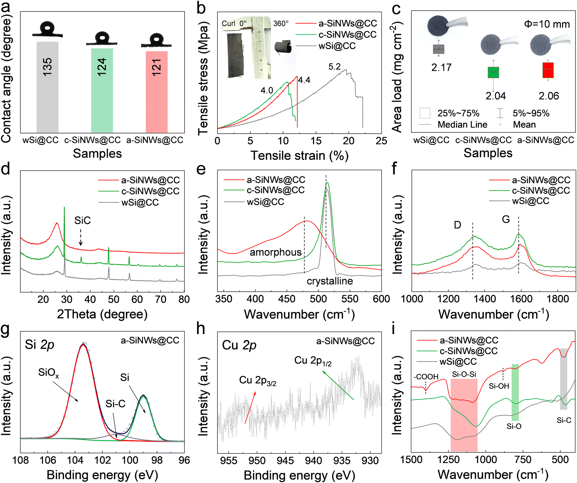 | ||
| Fig. 4 Characterization of the physical and chemical properties of wSi@CC, c-SiNWs@CC, and a-SiNWs@CC. (a) Contact angle, (b) horizontal tensile–strain curve (inset: bending demonstration), (c) active material mass area loading, (d) XRD patterns, (e) and (f) Raman spectra, and (g) and (h) Si 2p and Cu 2p spectra from the XPS analysis of a-SiNWs@CC, and (i) FTIR spectra. | ||
Furthermore, XPS characterization was performed to analyze the surface chemical bonding of the materials (Fig. 4g and h, and Fig. S23, ESI†). In the Si 2p spectrum of a-SiNWs@CC (Fig. 4g), typical peaks for Si, Si–C, and SiOx are observed. Combined with the C 1s and O 2p spectra in Fig. S23 (ESI†), this indicates a significant presence of surface functional groups on a-SiNWs@CC. In contrast, the Si 2p spectrum of c-SiNWs@CC shows a notably stronger Si–C peak, which likely results from the formation of SiC.38 Additionally, the peaks at 933 and 953 eV in the Cu 2p spectrum (Fig. 4h) correspond to the binding energies of Cu 2p1/2 and Cu 2p3/2. And, the absence of a distinct split peak suggests that Cu is predominantly in Cu0.29 The Fourier transform infrared spectra (FTIR) in Fig. 4i further clarified the chemical bonding states between Si, C, and O. The presence of chemical bonds is crucial for enhancing the structural stability and conductivity of the electrodes. Compared to wSi@CC and c-SiNWs@CC, the surfaces of a-SiNWs@CC are featured with additional functional groups such as –COOH and Si–OH. These results indicate that a-SiNWs@CC have a rich array of surface chemical bonds, which improve structural stability while allowing for rapid (de)lithiation.14
Electrochemical performance
As illustrated in Fig. 5, to validate the stable lithium storage capability of the flexible a-SiNWs@CC electrode material, electrochemical performance tests were conducted by assembling the prepared electrodes into both half-cells and full cells. During the charge–discharge process at a current of 0.2 A g−1 (Fig. 5a), the initial discharge capacity of a-SiNWs@CC reaches 3526 mA h g−1, with an ICE as high as 91.35%. In comparison, the discharge capacities and ICEs for wSi@CC and c-SiNWs@CC electrodes are 3412 mA h g−1 (87.21%) and 3354 mA h g−1 (82.05%), respectively. As shown in Fig. 5b, during cycling at 0.8 A g−1, the a-SiNWs@CC electrode demonstrates an average coulombic efficiency greater than 99.7%, with a minimal fluctuation in each cycle, indicating the stability of the electrode structure. Fig. 5c shows that, at a current of 0.8 A g−1, after 200 cycles, a-SiNWs@CC maintains a reversible capacity of nearly 2900 mA h g−1 (Fig. S18 (ESI†), and the areal capacity reached 5.6 mA h cm−2), with a retention rate of nearly 95% (at the same current). In contrast, c-SiNWs@CC exhibits a capacity of only 1600 mA h g−1 (3.0 mA h cm−2), losing more than half of their lithium, while wSi@CC shows rapid capacity decay after the current increase during the fourth cycle, indicating significant instability. Moreover, compared to the most recently reported Si nanowire electrodes (Fig. 5d and Table S6, ESI†), a-SiNWs@CC exhibits an exceptional ICE and capacity retention. The rate performance depicted in Fig. 5e and f further demonstrates the fast ion and electron transport capabilities of a-SiNWs@CC. Even when the current increases from 0.2 A g−1 to 8.0 A g−1, the capacity remains at 0.8 A h g−1. Upon returning to 0.2 A g−1, the capacity recovers to its initial value (>3200 mA h g−1). When switching the current to 2.0 A g−1 (Fig. 5f), the capacity remains at 2150 mA h g−1 after 250 cycles, further confirming the high structural stability of a-SiNWs@CC. | ||
| Fig. 5 Electrochemical performance. Half cell: (a) initial (dis)charge curves, (b) coulombic efficiency, (c) cycling curves (with the first 3 cycles at 0.2 A g−1), (d) comparison with the recently reported Si nanowire electrodes, (e) rate curves, and (f) cycling curves (continuing from Fig. 5e). Full cell: (g) initial (dis)charge curve, (h) coulombic efficiency, (i) cycling curves and (j)–(l) differential capacity (dQ/dV) versus voltage contour plots. | ||
Additionally, as shown in Fig. 5g–i, full cells were assembled using commercial LiFePO4 (LFP) cathodes paired with wSi@CC, a-SiNWs@CC, and a-SiNWs@CC anodes to evaluate their practical value. Under a charge–discharge rate of 1.0C (1.0C = 170 mA h g−1), a-SiNWs@CC clearly demonstrates stable coulombic efficiency (average >98.5%), with a reversible capacity of approximately 120 mA h g−1 after 200 cycles. In contrast, wSi@CC and c-SiNWs@CC exhibit significant fluctuations and relatively lower coulombic efficiency, along with a rapid decline in cycling stability. The differential capacity plots of the first 50 cycles for the wSi@CC, c-SiNWs@CC, and a-SiNWs@CC electrodes in the half cell tests (Fig. 5j–l) were analyzed. During the early cycles, all three samples exhibit distinct capacity peaks near 0.30 V and 0.45 V. As cycling progresses, the peak intensity near 0.45 V for the wSi@CC and c-SiNWs@CC electrodes gradually decreases, indicating capacity fade and structural degradation. For the wSi@CC electrode, the second peak slightly below 0.45 V and the reduced distance between peaks suggest severe electrode polarization and wSi aggregation. In contrast, the differential capacity plot of the a-SiNWs@CC electrode shows stable peak positions and intensity, indicating that this flexible electrode experiences lower electrode polarization and less Si aggregation during cycling, which contributes to its higher ICE and superior rate performance.26,39
In summary, the high ICE and stable electrochemical performance can be attributed to the following factors: (i) the isotropic nature of a-SiNWs provides excellent stress/strain tolerance. (ii) The well-distributed nanowires increase the reaction contact area, enhancing lithium insertion/extraction rates and efficiency. (iii) The majority of the prepared nanowires are smaller than 15 nm. For SiNWs, this nano size is significantly below the critical dimension for Si expansion (300–400 nm), facilitating the formation of a stable SEI layer.28,40
Enhancement mechanism and structural evolution during electrochemical cycling
To elucidate the stable lithium storage of a-SiNWs@CC materials, it is important to study their electronic/ionic transport kinetics. As shown in Fig. 6a–d and Fig. S25 (ESI†), the in situ electrochemical impedance spectra (EIS) and corresponding dynamic relaxation time (DRT) curves during the first (de)lithiation process were tested.41 The results indicate that a-SiNWs@CC exhibits a gradual decrease in impedance on a macroscopic scale, which subsequently stabilizes (Fig. 6a). Furthermore, in Fig. 6b, the EIS data were converted from the frequency domain to the time domain to obtain the DRT curves, which help decouple the highly overlapping physicochemical processes in the complex system. Typically, peaks with time constants τ in the range of 10−4 to 10−3 s are attributed to Li transport within the interface SEI layer. Notably, the a-SiNWs@CC electrode exhibits minimal peak fluctuations, indicating stable formation of the interface SEI layer during the initial (de)lithiation process, which enhances electronic/ionic migration rates. In contrast, as shown in Fig. 6c and Fig. S25 (ESI†), while c-SiNWs@CC and wSi@CC show similar trends in the EIS plots, they display significant fluctuations in the DRT curves (Fig. 6d and Fig. S25, ESI†). Particularly, the wSi@CC electrode material (Fig. S25, ESI†) shows substantial oscillations in both the EIS plot and the DRT curve, suggesting that the simple physical contact between wSi and carbon cloth impedes electron and ion transfer. Additionally, the volume changes in Si exacerbate the electrical contact issues, ultimately leading to deterioration of the electrode material. Further numerical fitting of the in situ EIS data was conducted using a general equivalent circuit model (Fig. S26, ESI†). To directly reflect the impedance changes during the (de)lithiation process, the SEI interface's diffusion impedance and the interfacial charge transfer impedance are combined into R. The results show that the prepared a-SiNWs@CC electrode exhibits smaller and more stable impedance, suggesting that this a-SiNW material is more favorable for stable lithium storage compared to crystalline Si nanowires and simple wSi. | ||
| Fig. 6 Kinetic properties. In situ EIS and corresponding DRT of (a) and (b) a-SiNWs@CC and (c) and (d) c-SiNWs@CC during the first (de)lithiation, (e) and (f) GITT test, (g) apparent ion diffusion values for the electrodes, and (h) schematic diagram of ion transport pathways and interface stability for different electrodes. | ||
Using the galvanostatic intermittent titration technique (GITT), the lithium-ion apparent diffusion coefficients for a-SiNWs@CC, c-SiNWs@CC, and wSi@CC electrodes during the first and second (de)lithiation cycles were calculated.42,43 As shown in Fig. 6e–g and Fig. S27 (ESI†), a relaxation time of 1 h and a pulse time of 20 min were set, with cycling conducted at a current of 0.2 A g−1 for two cycles. The calculated average lithium-ion apparent diffusion coefficients for a-SiNWs@CC, c-SiNWs@CC, and wSi@CC electrodes are 5.38 × 10⁻⁹, 4.04 × 10⁻⁹, and 8.60 × 10⁻¹⁰ cm2 s−1, respectively. Clearly, the a-SiNWs@CC electrode exhibits an excellent ion diffusion rate and remains relatively stable during both the first and second cycles, whereas the other electrode materials show significant variations (Fig. 6g).
In brief, Fig. 6h and Fig. S28 (ESI†) provide a clear illustration of the electron/ion transport structures for different electrodes. The exceptional transport kinetics of the a-SiNWs@CC can be attributed to two factors: first, the isotropy of a-Si compared to c-Si promotes the stable formation of the SEI layer. Second, the one-dimensional structure of Si nanowires, in contrast to traditional particles, offers continuous transport pathways, while Si particles have numerous physical contact points that significantly reduce lithium-ion transport efficiency. Consequently, a-SiNWs@CC exhibits lower charge transfer resistance and faster ion migration rates, demonstrating outstanding stability and rate performance.
To clearly illustrate the low-stress effect of the prepared a-SiNWs@CC electrode, a simplified finite element model was used to simulate the lithiation of a-Si and c-Si. Notably, to avoid prolonged computational times, a two-dimensional structural model was constructed (Fig. S29, ESI†). First, as shown in Fig. 7a and b, the von mises stress and elongation after the first lithiation in single particles of a-Si and c-Si clearly demonstrate that the isotropic nature of a-Si helps to alleviate stress concentrations.
 | ||
| Fig. 7 Simulation of the lithiation expansion of a-Si and c-Si and their interaction with carbon substrates. (a) and (b) Von mises stress (left) and elongation (right) of a-Si and c-Si, (c) von mises on the carbon substrate during Si lithiation at different time intervals, (d) the von mises curves for single-particle, (e) and (f) the electrode displacement, and the in von mises experienced by the carbon substrate. | ||
Furthermore, we simulated the lithiation process with multiple Si particles randomly distributed on the carbon substrate to capture the microscopic deformation details between them and the carbon-based electrode. As illustrated in Fig. 7c, with increasing lithiation time, Si particles expand, come into contact, and compress each other, leading to stress concentrations. In practice, an excessive force can result in the loss of electrical contact between the active material and the current collector. Evidently, a-Si exhibits a smoother stress distribution, indicating a lower degree of electrode damage. The stress variation in single particles at different lithiation states, as shown in Fig. 7d, further demonstrates the more favorable stress distribution of a-Si. Additionally, electrode expansion is a valuable indicator of battery performance. As shown in Fig. 7e and Fig. S30 (ESI†), the displacement of the electrode during the initial lithiation is simulated, and together with the stress variation curve on the carbon substrate in Fig. 7f, it strongly suggests that electrodes composed of a-Si exhibit a more stable structure.
In Fig. 8, the morphology of the electrodes after 100 cycles was characterized. The results indicated that all electrodes exhibited significant surface swelling after cycling, which is attributed to the formation of SEI films and other by-products generated during (de)lithiation. The a-SiNWs@CC maintains a clear nanowire outline on the surface after cycling (Fig. 8a and b). In contrast, the surface of c-SiNWs@CC shows more uneven impurities, and the carbon cloth substrate is clearly exposed (Fig. 8c and d), suggesting that some nanowires on the c-SiNWs@CC surface detach and lose electrical contact during cycling. The wSi@CC electrode experiences even more severe electrical contact failure and cracking (Fig. 8e and f).
 | ||
| Fig. 8 Surface morphology and composition of electrodes, and prospects for scalable production. Morphology of (a) and (b) a-SiNWs@CC, (c) and (d) c-SiNWs@CC, and (e) and (f) WSi@CC, (g) the relative area of components in the XPS spectra of different electrodes, (h) schematic comparison of SEI formation, and (i) prospective demonstration of scalable production. | ||
Additionally, the surface SEI components were characterized using XPS. Fig. 8g and Fig. S31 (ESI†) display the elemental spectra of O 1s, Li 1s, F 1s, Si 2p, and C 1s, as well as the relative content of Li2CO3 and LiF components. The results indicate that the a-SiNWs@CC surface has relatively less Li2CO3, suggesting that the stable growth of the SEI on its surface reduces the formation of Li2CO3 by suppressing the reduction of organic solvent decomposition products. A comparison of LiF intensity reveals that a-SiNWs@CC forms more LiF on its surface during (de)lithiation. This component, with a high elastic modulus and a low Li+ diffusion barrier can reduce SEI damage during the expansion of Si nanowires.44,45Fig. 8h and Fig. S32 (ESI†) provide simplified diagrams of the SEI composition on the Si surface of the three electrodes, illustrating that a thin, LiF-rich SEI forms on the surface of a-SiNWs@CC. In addition, Fig. 8i further proposed the high-efficiency preparation process of amplification, which is expected to provide a new idea for the preparation of high-performance flexible electrodes.
Conclusions
In summary, a new strategy to fundamentally reconstruct the microstructure of photovoltaic waste silicon (wSi) is developed by inducing the growth of a-SiNWs, leveraging the oxidative properties of wSi. The high-gradient thermal field (ca. 4.2 × 10³ K s−1) provided by CTS is utilized to break the traditional slow heating and cooling rates. Under the confinement of the oxide film, Si atoms precipitate in a one-dimensional direction, while Cu melt catalysis promotes the rapid in situ growth of amorphous nanowires on the surface of carbon cloth. The growth mechanism of a-SiNWs@CC was proposed, confirming that the introduction of Cu was the primary factor driving the formation of a-SiNWs. The resulting a-SiNWs@CC exhibits outstanding lithium storage performance, with an initial coulombic efficiency of 91.35% at 0.2 A g−1 and a retained capacity of 2150 mA h g−1 after 250 cycles at 2.0 A g−1. The enhanced electron/ion transport kinetics of the a-SiNWs@CC electrode were elucidated, contributing to improved structural integrity and stability during (de)lithiation. Additionally, the surface morphology and micro-composition of a-SiNWs@CC after cycling were revealed, and a roll-to-roll continuous production process for large-scale fabrication was proposed. Consequently, the successful implementation of this method opens up new possibilities for optimization and re-utilisation of wSi.Experimental
Sample preparation
The wSi used in this paper was provided by JA Co., LTD. In the process of diamond wire cutting silicon ingot, a large amount of the silicon slurry was produced, and wSi was obtained by simple evaporation, drying and crushing. Other reagents were used directly without any treatment.First, wSi was weighed and added to deionized water to prepare a suspension with a solid content of 5 wt%. Then, a certain amount of Cu sulfate pentahydrate (CuSO4·5H2O) was added to the suspension, followed by sonication for 30 min to disperse the mixture (the mass of CuSO4·5H2O was calculated based on 3 wt% of the wSi mass by first determining the mass of elemental Cu and then converting it to the corresponding Cu salt mass). Next, clean carbon cloth was cut into small pieces (ca. 1 × 4 cm) and immersed in the suspension. After stirring for 2 h, the pieces were removed and placed in a vacuum drying oven set at 80 °C for 10 h. Finally, the carbon cloth with the attached mixture was secured at both ends in the graphite clamps of a CTS device (an Ar atmosphere containing 5 wt% H2). By applying a voltage of 30 V, a current of 60 A, and a shock time of 0.5 s, the a-SiNWs@CC electrode was successfully prepared.
For comparison, the c-SiNWs@CC electrode was prepared by omitting the addition of CuSO4·5H2O in the above steps, while keeping the rest of the procedure unchanged. Furthermore, a single electrode without CTS and without the introduction of Cu was labeled as wSi@CC. Additionally, the growth of nanowires under different CTS conditions was briefly explored (see the ESI† for details).
Material characterization
The morphology and structure of the samples were characterized using scanning electron microscopy (SEM, JSM-7800 Prime) and transmission electron microscopy (TEM, JEM-2100F). A laser particle size analyzer (Mastersizer 2000) was used to characterize the particle size distribution, and Raman spectra were recorded using a 532 nm excitation wavelength. The material's purity was measured using inductively coupled plasma atomic emission spectroscopy (ICP). The contact angles of the samples at different temperatures were measured using a high-temperature contact angle tester (OCA25-HTV1800). The tensile-strain curves of different samples were tested using a universal testing machine (Zwick Z250). X-ray diffraction (XRD) patterns were measured using an X-ray diffractometer (Cu-Kα radiation, 40 mA, 40 kV). X-ray photoelectron spectroscopy (XPS) analysis was performed using an ESCALAB 250Xi spectrometer. The purity of the wSi powder was determined using inductively coupled plasma atomic emission spectroscopy (ICP-AES, Optima 7000DV). The CTS equipment was purchased from Saiyin New Materials Technology Co., Ltd.Electrochemical characterization
The a-SiNWs@CC, c-SiNWs@CC, and wSi@CC samples were cut into small circular discs with a diameter of 10 mm and directly used as working electrodes (a thickness of ca. 360 μm) without any binders or conductive agents. In half cell tests, the lithium metal was used as the counter electrode, and the electrolyte consisted of 1 M LiPF6 in a mixture of ethylene carbonate and diethyl carbonate (1:1, vol%) with 5 wt% fluoroethylene carbonate, separated from the working electrode by a microporous polypropylene membrane (Celgard, 2400). The electrochemical cycling and rate performance of the half cells were evaluated within a voltage window of 0.01–3.0 V. In full cell tests, the prepared anodes were prelithiated three times (cycled at 0.2 A g−1 in the half cell) and then paired with LiFePO4 (LFP) cathodes to assemble the full cells (N/P ratio of 1.1). The separator and electrolyte used were the same as those in the half-cells. The cathode was prepared by mixing commercial LFP, polyvinylidene fluoride, and conductive carbon black in an 8:1:1 ratio, coating the mixture onto an aluminum current collector, and vacuum drying at 110 °C for 12 h. The electrochemical performance of the full cells was evaluated within a voltage window of 2.4–3.6 V. Cell assembly was conducted in an argon-filled glove box, with all cells using C2032-type coin cells. Constant current charge–discharge, galvanostatic intermittent titration technique (GITT) tests, and specific capacity calculations based on the mass of active materials were carried out using a NEWARE battery testing system (CT-4008T-5V50 mA-164, Shenzhen, China). Electrochemical impedance spectroscopy (EIS) measurements were performed using a CHI760E electrochemical workstation (Shanghai CH Instrument Company, China) in a frequency range from 100 kHz to 0.01 Hz.
Author contributions
L. S. conceived the ideas, designed the research plan, and wrote the paper; S. L. and Z. J. prepared the materials and performed the majority of the materials characterization and electrochemical tests; L. S. performed the electrochemical tests; Y. W., F. X. and S. L. carried out the XPS and Raman measurements; J. L. performed the simulation and calculation; Z. T. carried out the EIS measurement; J. L., S. L. and K. S. helped the paper writing; W. M. and X. H. supervised the whole project. All authors discussed and commented on the manuscript.Data availability
The data supporting this article have been included as part of the ESI.†Conflicts of interest
The authors declare that they have no known competing financial interests or personal relationships that could have appeared to influence the work reported in this paper.Acknowledgements
This work was supported by the National Key R&D Program of China (2024YFC3907601-3), the Major Science and Technology Projects in Yunnan Province (No. 202402AF080005), the National Natural Science Foundation of China (No. 22468029, 52274408), the Yunnan Fundamental Research Projects (No. 202401BE070001-013, 202201AW070014), the Yunnan Provincial Department of Education university service key industrial science and technology project (No. FWCY-BSPY2024036) and the Program for Innovative Research Team in University of Ministry of Education of China (No. IRT 17R48). K. S. acknowledges the Australian Research Council (ARC) Discovery Early Career Researcher Award (DE230100021) and support from the Australian Centre of Advanced Photovoltaics (ACAP) as a recipient of the ACAP Fellowship (RG172864-B). X. H. acknowledges the financial support of the Australian Research Council (ARC) Future Fellowship (FT190100756).References
- C. Ballif, F.-J. Haug, M. Boccard, P. J. Verlinden and G. Hahn, Nat. Rev. Mater., 2022, 7, 597–616 CrossRef
.
- Z. Liu, S. E. Sofia, H. S. Laine, M. Woodhouse, S. Wieghold, I. M. Peters and T. Buonassisi, Energy Environ. Sci., 2020, 13, 12–23 Search PubMed
- J. Lu, S. Liu, J. Liu, G. Qian, D. Wang, X. Gong, Y. Deng, Y. Chen and Z. Wang, Adv. Energy Mater., 2021, 11, 2102103 Search PubMed
- X. Li, G. Lv, W. Ma, T. Li, R. Zhang, J. Zhang, S. Li and Y. Lei, J. Hazard. Mater., 2022, 424, 127389 Search PubMed
- K. Wang, X.-B. Zhong, Y.-X. Song, Y.-H. Zhang, Y.-G. Zhang, X.-G. You, P.-G. Ji, K. M. Shodievich, U. Khalilov and G.-K. Wang, Rare Met., 2024, 43, 1–13 Search PubMed
- D. Wei, J. Kong, S. Gao, S. Zhou, Y. Zhuang and P. Xing, J. Environ. Manage., 2021, 290, 112548 CrossRef PubMed
- W. Liu, J. Tian, D. Xiang, R. Mao and B. Wang, J. Cleaner Prod., 2020, 274, 122799 Search PubMed
- G. Qian, Y. Sun, Z. Wang, K. Wei and W. Ma, ACS Sustainable Chem. Eng., 2021, 9, 2962–2974 CrossRef CAS
- J. Cao, Y. Sim, X. Y. Tan, J. Zheng, S. W. Chien, N. Jia, K. Chen, Y. B. Tay, J. F. Dong and L. Yang, Adv. Mater., 2022, 34, 2110518 Search PubMed
- Y. Yang, S. Biswas, R. Xu, X. Xiao, X. Xu, P. Zhang, H. Gong, X. Zheng, Y. Peng and J. Li, Science, 2024, 386, 322–327 CrossRef CAS PubMed
- L. Zhang, Q. Huang, X. Liao, Y. Dou, P. Liu, M. Al-Mamun, Y. Wang, S. Zhang, S. Zhao, D. Wang, G. Meng and H. Zhao, Energy Environ. Sci., 2021, 14, 3502–3509 RSC
- T. Liu, T. Dong, M. Wang, X. Du, Y. Sun, G. Xu, H. Zhang, S. Dong and G. Cui, Nat. Sustainable, 2024, 7, 1057–1066 Search PubMed
- T. Hu, H. Zhou, J. Tang, S. Chen, Z. Li, X. Yu, Y. Zhang, J. Yang and X. Zhou, Energy Environ. Sci., 2024, 17, 6377–6392 RSC
- L. Wang, J. J. Lu, S. Y. Li, F. S. Xi, Z. Q. Tong, X. H. Chen, K. X. Wei and W. H. Ma, Adv. Funct. Mater., 2024, 34, 2403574 Search PubMed
- C. Xu, L. Shen, W. Zhang, Y. Huang, Z. Sun, G. Zhao, Y. Lin, Q. Zhang, Z. Huang and J. Li, Energy Storage Mater., 2023, 56, 319–330 CrossRef
- S.
H. Bhimineni, S. T. Ko, C. Cornwell, Y. Xia, S. H. Tolbert, J. Luo and P. Sautet, Adv. Energy Mater., 2024, 14, 2400924 CrossRef CAS
- S. Chae, Y. Xu, R. Yi, H. S. Lim, D. Velickovic, X. Li, Q. Li, C. Wang and J. G. Zhang, Adv. Mater., 2021, 33, 2103095 Search PubMed
- S. Surdo and G. Barillaro, Small, 2024, 20, 2400499 CrossRef CAS PubMed
- J. B. Fang, Y. Q. Cao, S. Z. Chang, F. R. Teng, D. Wu and A. D. Li, Adv. Funct. Mater., 2021, 32, 2109682 CrossRef
- S. A. Ahad, T. Kennedy and H. Geaney, ACS Energy Lett., 2024, 9, 1548–1561 CrossRef CAS PubMed
- S. Raman, A. R. Sankar and M. Sindhuja, Nanotechnology, 2023, 34, 182001 CrossRef CAS PubMed
- Z. Li, M. Han, P. Yu, J. Lin and J. Yu, Nano-Micro Lett., 2024, 16, 98 CrossRef CAS PubMed
- L. Lin, X. Xu, C. Chu, M. K. Majeed and J. Yang, Angew. Chem., Int. Ed., 2016, 55, 14063–14066 Search PubMed
- Z. Wang, Y. Li, S. Huang, L. Liu, Y. Wang, J. Jin, D. Kong, L. Zhang and O. G. Schmidt, J. Mater. Chem. A, 2020, 8, 4836–4843 Search PubMed
- A. A. Leonardi, M. J. L. Faro and A. Irrera, Nanomaterials, 2021, 11, 383 Search PubMed
- A. Pendashteh, R. Tomey and J. J. Vilatela, Adv. Energy Mater., 2024, 14, 2304018 CrossRef CAS
- Y. Dong, T. Slade, M. J. Stolt, L. Li, S. N. Girard, L. Mai and S. Jin, Angew. Chem., Int. Ed., 2017, 56, 14453–14457 CrossRef CAS PubMed
- J. Lu, J. Liu, X. Gong, S. Pang, C. Zhou, H. Li, G. Qian and Z. Wang, Energy Storage Mater., 2022, 46, 594–604 Search PubMed
- L. Shen, P. Wang, C. Fang, Z. Lin, G. Zhao, S. Li, Y. Lin, Z. Huang and J. Li, Small, 2024, 20, 2404135 CrossRef CAS PubMed
- B. Liu, J. Sun, L. Zhou, P. Zhang, C. Yan and Q. Fu, J. Adv. Ceram., 2022, 11, 1417–1430 CrossRef CAS
- Y. Wan, Z. Wang, Y. Fang, Z. Xia, Y. Wang and J. Sha, Mater. Lett., 2010, 64, 1839–1842 CrossRef CAS
- V. A. Nebol'sin, J. Johansson, D. B. Suyatin and B. A. Spiridonov, J. Cryst. Growth, 2019, 505, 52–58 Search PubMed
- R. Tripathi, V. Chauhan, P. Gandharapu, S. Kobi, A. Mukhopadhyay and R. O. Dusane, ACS Appl. Nano Mater., 2022, 5, 17767–17782 CrossRef CAS
- Z. Yuan, C. Wang, K. Chen, Z. Ni and Y. Chen, Nanoscale Res. Lett., 2017, 12, 1–8 CrossRef CAS PubMed
- É. Ngo, W. Wang, P. Bulkin, I. Florea, M. Foldyna, P. Roca i Cabarrocas and J.-L. Maurice, J. Phys. Chem. C, 2021, 125, 19773–19779 CrossRef
- X. Li, F. Chen, B. Zhao, S. Zhang, X. Zheng, Y. Wang, X. Jin, C. Dai, J. Wang, J. Xie, Z. Zhang and Y. Zhao, Nano-Micro Lett., 2023, 15, 32 CrossRef PubMed
- F. Yang, P. Deng, H. He, R. Hong, K. Xiang, Y. Cao, B. Yu, Z. Xie, J. Lu and Z. Liu, Chem. Eng. J., 2024, 494, 152828 CrossRef CAS
- T. Lee, N. Kim, J. Lee, Y. Lee, J. Sung, H. Kim, S. Chae, H. Cha, Y. Son, S. K. Kwak and J. Cho, Adv. Energy Mater., 2023, 13, 2301139 Search PubMed
- Y. F. Tian, G. Li, D. X. Xu, Z. Y. Lu, M. Y. Yan, J. Wan, J. Y. Li, Q. Xu, S. Xin and R. Wen, Adv. Mater., 2022, 34, 2200672 Search PubMed
- Y. Sun, N. Liu and Y. Cui, Nat. Energy, 2016, 1, 1–12 Search PubMed
- A. Maradesa, B. Py, J. Huang, Y. Lu, P. Iurilli, A. Mrozinski, H. M. Law, Y. Wang, Z. Wang, J. Li, S. Xu, Q. Meyer, J. Liu, C. Brivio, A. Gavrilyuk, K. Kobayashi, A. Bertei, N. J. Williams, C. Zhao, M. Danzer, M. Zic, P. Wu, V. Yrjänä, S. Pereverzyev, Y. Chen, A. Weber, S. V. Kalinin, J. P. Schmidt, Y. Tsur, B. A. Boukamp, Q. Zhang, M. Gaberšček, R. O’Hayre and F. Ciucci, Joule, 2024, 8, 1958–1981 CrossRef CAS
- X. Lin, J. Gao, K. Zhong, Y. Huang, H. Yao, Y. Lin, Y. Zheng, Z. Huang and J. Li, J. Mater. Chem. A, 2022, 10, 23103–23112 Search PubMed
- L. Shen, C. Xu, J. Gao, J. Tao, Q. Zhang, Y. Chen, Y. Lin, Z. Huang and J. Li, J. Energy Chem., 2023, 77, 348–358 CrossRef CAS
- N. M. Johnson, Z. Yang, M. Kim, D.-J. Yoo, Q. Liu and Z. Zhang, ACS Energy Lett., 2022, 7, 897–905 CrossRef CAS
- Q. Fang, S. Xu, X. Sha, D. Liu, X. Zhang, W. Li, S. Weng, X. Li, L. Chen, H. Li, B. Wang, Z. Wang and X. Wang, Energy Environ. Sci., 2024, 17, 6368–6376 RSC
Footnotes |
| † Electronic supplementary information (ESI) available. See DOI: https://doi.org/10.1039/d5ee00020c |
| ‡ Liao Shen, Kaiwen Sun and Fengshuo Xi contributed equally to this study. |
| This journal is © The Royal Society of Chemistry 2025 |