
 Open Access Article
 This Open Access Article is licensed under a
 Creative Commons Attribution 3.0 Unported Licence
Transfer dynamics of photo-generated carriers in catalysis
Jun
Wang
ab,
Wanru
Liao
ab,
Yao
Tan
a,
Olivier
Henrotte
cd,
Yicui
Kang
c,
Kang
Liu
 a,
Junwei
Fu
a,
Zhang
Lin
e,
Liyuan
Chai
e,
Emiliano
Cortes
*c and
Min
Liu
*a
a,
Junwei
Fu
a,
Zhang
Lin
e,
Liyuan
Chai
e,
Emiliano
Cortes
*c and
Min
Liu
*a
aHunan Joint International Research Center for Carbon Dioxide Resource Utilization, State Key Laboratory of Powder Metallurgy, School of Physics, Central South University, Changsha 410083, Hunan, P.R. China. E-mail: minliu@csu.edu.cn
bSchool of Chemistry and Chemical Engineering, Changsha University of Science and Technology, Changsha 410114, Hunan, P.R. China
cNanoinstitut München, Fakultät für Physik, Ludwig-Maximilians-Universität München, 80539 München, Germany. E-mail: Emiliano.Cortes@lmu.de
dRegional Centre of Advanced Technologies and Materials Department, Czech Advanced Technology and Research Institute, Palacký University Olomouc, Olomouc 78371, Czech Republic
eSchool of Metallurgy and Environment, Central South University, Changsha 410083, Hunan, P.R. China
First published on 9th June 2025
Abstract
Semiconductor based photo-assisted catalytic reaction, leveraging solar energy for chemical fuel production and pollutant treatment, relies heavily on carrier separation and migration. Despite extensive efforts to enhance carrier separation, understanding carrier transfer dynamics remains limited, hindering large-scale application. This review systematically examines carrier transfer dynamics characterization, highlighting semiconductors' intrinsic properties, carrier relaxation methods, and spatiotemporal visualization. We also discuss plasmonic metal catalysts, a novel photocatalyst class with unique carrier dynamics. Furthermore, we evaluate advanced techniques and metrics for assessing carrier transfer, offering insights for developing high-performance catalysts. Finally, we provide a summary and outlook on future developments and standards in carrier transfer dynamics characterization for improved photo-related catalytic applications.
 Jun Wang | Jun Wang received his PhD (2021) degree from School of Metallurgy and Environment, Central South University. After two-years of post-doctoral training with Professor Min Liu at Central South University, he joined Changsha University of Science and Technology in 2023. His research interest focuses on semiconductor-based photocatalytic and photoelectrochemical water splitting. |
 Emiliano Cortes | Emiliano Cortés is Professor in Experimental Physics and Energy Conversion at the Faculty of Physics, University of Munich (LMU), Germany and he is the head of the Nanomaterials for Energy group. His research centers on the intersection of chemistry and physics, with an emphasis on creating plasmonic and photonic nanomaterials for energy harvesting, conversion, and storage, along with innovative methods to explore the fundamental processes involved. |
 Min Liu | Min Liu received his PhD (2010) degree from the Institute of Electrical Engineering, Chinese Academy of Sciences. In 2010–2015, he worked in University of Tokyo as a postdoctoral fellow with the guidance of Prof. Kazuhito Hashimoto and Prof. Kazunari Domen. In 2015–2017, he joined the University of Toronto as a postdoctoral fellow under the guidance of Prof. Edward Sargent. Since 2017, he is a professor in Central South University. His research interests focus on greenhouse gas reduction and energy catalysis, including the resource utilization of perfluorocarbon, electrocatalytic CO2 reduction, and photo(electro)chemical water splitting. |
1. Introduction
With the advancement of global industrialization, the continuous extraction of fossil fuels and the non-compliant emission of harmful substances have led to an increasing energy crisis and environmental pollution, becoming two major challenges faced by all humanity.1–3 In line with the United Nations’ Envision 2030 agenda, which encompasses 17 Sustainable Development Goals, achieving “affordable and clean energy” stands out as a global imperative. To meet this goal, it is urgent to develop and utilize new energy, for establishing a resource-saving and environmentally friendly society. The direct utilization of inexhaustible and green solar energy, through semiconductor-based photo-related catalysis (photocatalysis, photoelectrochemical catalysis, plasmonic catalysis, etc.), has emerged as a promising solution for both production of valuable chemical fuels and the treatment of harmful pollutants, holding the potential to mitigate the global energy crisis and address climate-related challenges.4–7Since the innovative work on TiO2-based photocatalysis by Fujishima and Honda in 1972,8 numerous semiconductors have been developed and investigated for diverse photo-related catalytic applications, including water splitting, CO2 reduction, ammonia synthesis, pollutants treatment (dyes, antibiotics, and heavy metals, etc.), analytes quantification, and organic synthesis, etc.9–16 As the workhorse to convert solar energy, this system provides flexibility in sequential energy transport and storage, receiving a significant amount of research investments.17–19 Among various components, the photoactive semiconductor acts as the heart of the system which dominates the light absorption, photo-carrier transfer, and the surface catalytic reactions.20,21 Under illumination, the semiconductors with suitable band gaps absorb light energy to trigger the excitation of the valence electrons from valence band (VB) to the conduction band (CB), generating photo-induced holes in the VB. The electrons in the CB and the holes in the VB generally face two possible fates: (1) undergo the desired transport which separate from each other to reach the semiconductor surface; or (2) recombine in the bulk or at the surface of the semiconductor. Once the carrier finally arrives at the surface, they participate in the redox reactions of the reactants, utilizing solar energy to produce chemical fuels or to degrade the toxic pollutants.22,23
Generally, the light-to-chemical energy efficiency is equal to the product of the efficiencies of light capture, photo-generated carrier separation, and the surface catalytic reaction. However, the Coulomb force between photo generated electron and hole, and the difference in time scale between carrier transfer (μs to ms) and surface catalytic reaction (ms to s) leads to inevitable carrier recombination.24,25 Various factors including defects and grain boundaries (which may act as carrier trap centers), conductivity and carrier mobility (intrinsic physical properties), as well as geometric dimensions and crystallinity (phase structures), would jointly affect the carrier transfer rate within bulk catalyst.26,27 For instance, a lower dielectric constant often leads to the formation of entangled/bound excitons (lifetime ranges from ps and ns) between holes and electrons in polymeric semiconductors after excitation.28,29 The longer the exciton lifetime, the fewer available photo-generated electrons and holes, and the energy is usually dissipated in the form of luminescence, which affects the photocatalytic performance. Intrinsic defects (point defects, line defect, etc.) are inevitable in nanomaterials, and act as either carrier recombination center (deep level impurity) or carrier trap sites (shallow level impurity) to influence the carrier transfer dynamics. Usually, anion vacancies with relatively low content are well-recognized as carrier trap sites to promote the separation of electrons and holes. The lifetime of trapped electrons/holes varies within a wide range from ns to ms.30–32 Thus, the separation of photo-generated carriers is a complex process of multiple time and space scales, and the sluggish carrier transfer dynamics has become the main obstacle that hinders the catalytic activity, urging in-depth investigation of the carrier transfer dynamics for desirable solar energy conversion.33,34
To overcome these limitations, various strategies have been developed and designed to promote the carrier transfer, including heterojunction, atom doping, crystal facet regulation, defects engineering, single atom, ligand engineering, etc.26,35–37 These approaches facilitate the electron–hole pair separation through the regulation of built-in electric field, energy band structure, density of states, and carrier transfer routes. Besides the above traditional methods, metal–semiconductor heterojunctions have emerged as a promising strategy for enhancing both sunlight absorption and charge carrier dynamics.38–40 Among metal nanoparticles, plasmonic materials (e.g., Au, Ag, Cu, Al) leverage localized surface plasmon resonance (LSPR) to harvest light across a broad spectrum, including the visible and near-infrared regions, which are underutilized by conventional semiconductors.41,42 When integrated into heterojunctions with semiconductors, plasmonic materials not only extend the range of light absorption but also improve charge separation and transfer through enhanced local electric fields and hot carrier injection. This synergistic effect optimizes both the light-capturing capacity and the charge carrier dynamics, addressing the bottlenecks of recombination and slow transfer rates.15 Consequently, plasmonic-semiconductor hybrid systems offer a robust platform for improving photocatalytic performance, facilitating efficient solar-to-chemical energy conversion. However, the investigation of such hybrid systems remains highly challenging due to the complexity of the processes involved, which span multiple spatial and temporal scales. This necessitates advanced analytical methods to capture and correlate phenomena occurring at different resolutions, including the nanoscale structure, ultrafast carrier dynamics, and macroscopic catalytic performance.
At present, numerous characterization methods have been developed based on the frequency- and time-domain analysis (including open-circuit photovoltage (Vph), and intensity-modulated photocurrent/photovoltage spectroscopy (IMPS/IMVS)),43,44 the degree of carrier recombination (such as photoluminescence (PL) and time-resolved photoluminescence (TRPL)),45–47 and the transmission rate or efficiency (including photoelectrochemical impedance spectroscopy (PEIS) and transient photocurrent/photovoltage (TPC/TPV)).48,49 Beyond the traditional characterization approaches, temperature-dependent PL (TDPL) spectroscopy, transient absorption spectroscopy (TAS), space-charged limited current (SCLC), kelvin probe force microscopy (KPFM), scanning photoelectrochemical microscopy (SPECM), and spatiotemporally resolved surface photovoltage (SRSPV) measurements newly emerge as powerful tools not only to unveil the intrinsic semiconductor properties,50–53 but also to realize the visualization of the carrier separation process (Fig. 1). These techniques can provide new approaches and act as complementary tools for further understanding the distribution and transport of charge carriers in time and space scales.
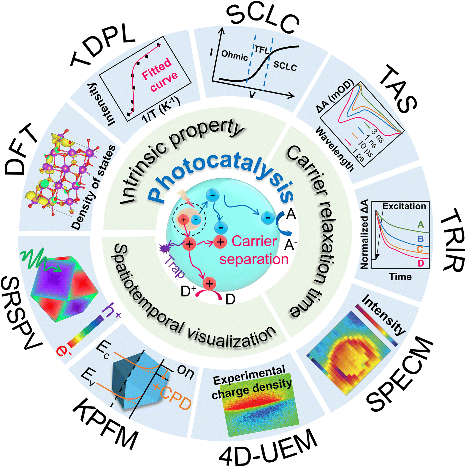 | ||
| Fig. 1 Schematic diagram for photo-related catalytic process, carrier migration, and the advanced characterizations for probing carrier transfer dynamics. D: electron donor. A: electron acceptor. TRPL: time-resolved photoluminescence. SCLC: space-charged limited current. TAS: transient absorption spectroscopy. TRIR: time-resolved infrared. SPECM: scanning photoelectrochemical microscopy. 4D-UEM: four-dimensional ultrafast electron microscopy. KPFM: kelvin probe force microscopy. SRSPV: spatiotemporally resolved surface photovoltage. DFT: density functional theory. | ||
In this review, we first introduce the fundamentals of photocatalysis, and highlights the vital role of rapid carrier transfer to achieve high-performance photo(electro)catalytic applications. We discuss the importance of the performance metrics employed to compare effectively the photodevices. Secondly, several traditional and novel characterization methods for monitoring carrier transfer dynamics in traditional semiconductors are summarized, including equipment construction, testing principles, operating procedures, and sample preparation process, followed by the specific applications and corresponding mechanism analysis. The systematic and in-depth discussion about the carrier transfer dynamics characterizations would unveil the carrier migration and recombination mechanism from various perspectives (for instance, the probability and means of recombination, carrier lifetime, semiconductors’ intrinsic properties, and the visualization of transmission processes, among others), furnishing guidance for high-performance photoactive materials design. At the last paragraph of each method, we summarized the characteristics of the technology and analyzed the limitations and challenges in practical application. Towards the end, we briefly explore the novel aspect in the realm of photoactive materials, involving plasmonic (metal) nanostructures, where carrier dynamics differ significantly from those of traditional semiconductor materials.54,55 Unlike traditional systems, plasmonic materials exhibit complex phenomena upon light excitation, including hot-carrier generation, localized heating (photothermal effects), and enhanced electromagnetic fields. These intertwined effects introduce new challenges in characterizing and understanding carrier behavior. Consequently, studying plasmonic systems requires not only the presented advanced experimental and theoretical tools, but also the development of new or combined methodologies that go beyond those typically used for conventional semiconductors. We outline the benefits and limitations associated with plasmonic metals and discuss strategies to address the intrinsic drawbacks of both semiconductors and metals. Emphasis is placed on the role of solid interfaces in optimizing charge transfer processes, facilitating the transition from single-material systems to advanced hybrid configurations. Finally, we provide our perspective on the application scenarios of the different characterization methods discussed. This includes the standardization and harmonization of metrics, as well as the future development of novel methods and technologies to advance further in the field of solar-to-fuels conversion.
2. Fundamental principles
For a typical photo-excitation catalytic process, the photoactive materials would first absorb solar light to form photo-induced electron–hole pairs. Then, the generated carriers undergo the migration and recombination in the semiconductors. Finally, the carriers reached surface to participate in the interfacial redox reactions, converting solar light to electricity for energy and environmental-related catalytic applications.2.1. Light harvesting
Light harvesting is the first step of photocatalytic processes. Light absorption ability determines the maximum solar energy conversion efficiency.56–58 Generally, only the photons with energy equal or larger than the band gap energy of the semiconductors can excite the electrons from the VB to the CB, while leaving holes in the VB. The relationship between the band gap and the sunlight wavelength (λ) can be described as: .
.
The widely utilized semiconductors, such as metal oxides, sulfides, and nitrides (including single metal and multi metals), usually exhibit band gaps ranging from 2.0 to 3.5 eV,59–61 suggesting the limited utilization of solar spectrum. To extend the light harvesting ability of the broad bandgap semiconductors, numerous efforts have been devoted. At present, various strategies including oxygen vacancy (VO),62 heteroatom doping,63 antireflective layer decoration,64 and of nano-semiconductors arrangement65 have all been verified for enhancing the light harvesting ability of semiconductors. In addition to traditional semiconductors, nanometals (Au, Ag, Al, Cu, etc.) with the nanometric size range also exhibited strong light harvesting ability, due to their unique LSPR properties.40,66,67 Under light illumination, the photon energy excites the free electrons which oscillates on the surface of the metal nanoparticles. The oscillation is greatly affected by the Coulomb force, causing the electrons to reciprocate near the equilibrium position. Once the frequency of the incident light coincides with the oscillation frequency of the free electrons, at this point, the amplitude of the electron oscillations increases significantly, creating hot carriers (electrons and holes) and electromagnetic field. By changing the size and morphology, the light absorption range of the nanometal is tunable over the entire solar spectrum.55,68
2.2. Carrier separation
After the excitation under illumination, the photo-induced carriers undergo the migration and separation processes within the photocatalysts, and are eventually transferred to the surface to take part in the redox reaction. However, the Coulomb force between the electrons in CB and the holes in VB lead to severe recombination of the carriers, even under applied bias.22,69 Also, there exists order of magnitude difference between carrier recombination and surface reaction kinetics on the time scale, contributing severe recombination of the carriers.36 In general, sluggish carrier transfer has been well-accepted as the key factor that hindered the cactalytic performance, as the photoexcited electrons tend to relax back to the valence band to recombine with holes. For addressing this issue, constructing heterostructure, including typical type-II, Z-scheme, and S-scheme,70–73 is proved as a universal and effective means. Besides, Li et al. designed a gradient Mg doping strategy into Ta3N5, to induce a gradient of the band edge energetics which greatly enhances the charge separation efficiency.74 Recently, subsurface VOs were demonstrated to inhibit the surface Fermi level pinning effect and boost the open-circuit photovoltage in metal oxide semiconductors, significantly promoting the surface carrier transfer.75 In addition, nanostructure regulation, interfacial chemical bond construction, metal–semiconductor junction, and built-in electric field strategies were developed for efficient carrier transfer.76–80For semiconductors with low dielectric constants, Coulomb interaction between electrons and holes led to the formation of a bound state system (i.e., exciton).81,82 Usually, excitons acted as the scattering center, which hindered the separation of electrons and holes. To facilitate the dissociation of excitons, strategies including heteroatom doping,83 ligand modification,84 and linear donor–acceptor construction85 were developed.
The introduction of defects in photocatalysts was inevitable since the preparation of nanomaterials often involved complex physical or chemical processes.86 In the photocatalytic process, although most defects may act as carrier scattering or recombination centers, resulting in a decrease in the separation efficiency of holes and electrons. However, some defects such as oxygen vacancies can act as trap centers, promoting the separation of photogenerated carriers by capturing electrons/holes.87,88 It is worth noting that in order to fully exploit the trapping effect of these defects, the defect concentration usually needs to be precisely regulated.
Traditional photocatalytic oxidation and reduction reactions occur simultaneously on the catalyst surface, and this spatial overlap inevitably increases the probability of surface carrier recombination. By anchoring the photoactive materials on a conductive surface, the photogenerated holes and electrons can be separated effectively in space, thanks to an applied bias driving the unwanted carriers through an external electrical circuit. Choosing n-type semiconductor as example, under illumination and applied bias, the photogenerated holes can be transferred to the catalyst surface interacting with the reactants, while the electrons are transferred to the conductive surface, driven through an external circuit, and finally reacting at a counter electrode. This process is defined as photoelectrocatalysis. Photocatalysis and photoelectrocatalysis are both based on the photoelectric effect of semiconductors, while the introduction of external circuit in photoelectrocatalysis helps the spatial separation of photocarriers. The applied bias is lower than the redox potential of the reactant, providing only a certain driving force for this carrier separation, while avoiding unwanted side reactions at the photoactive materials.
2.3. Surface reaction
When the photo-generated electrons and holes reached the semiconductors surface, they interacted with the reactants, enabling solar-to-energy conversion. However, a semiconductor surface with insufficient catalytic sites exhibits sluggish surface catalytic kinetics. Various modification strategies – such as co-catalysts decoration,89 surface defects engineering,90 and carrier transport layer loading91 – have been widely adopted to decrease the reaction energy barrier, and facilitate near unity utilization of the surface carriers.Despite significant efforts devoted to enhancing the solar light harvesting and surface catalytic kinetics, limited charge carrier transfer efficiency remains a major bottleneck hindering broader photocatalytic applicability.92–94 Thus, an in-depth understanding of the carrier transfer dynamics is necessary for the development of high-performance photocatalytic systems, opening new avenues for both fundamental research and practical applications across various scientific domains.
2.4 Performance metrics
The fundamental processes of photocatalytic and photoelectrocatalytic (PEC) technologies involve charge carrier generation, separation, and surface catalytic reactions. However, due to the integration of electrochemical methods in PEC systems, the evaluation of photocatalytic and PEC processes differs significantly, especially in terms of performance metrics. The typically reported performance metrics used in the field are discussed below. Table 1 summarizes the metrics that are widely utilized in photocatalytic and PEC processes for comparison, and the specific calculation formulas are displayed in Table 2.| Performance metrics | Photocatalysts | Photoelectrocatalysts |
|---|---|---|
| Activity | Formation rate (μmol g−1 h−1) | Photocurrent density (mA cm−2) |
| Apparent quantum yield (%) | Onset potential (mV) | |
| Turnover frequency (h−1) | Open circuit photovoltage (V) | |
| Apparent quantum efficiency (%) | Applied bias photon-to-current efficiency (%) | |
| Incident-photon-to-current conversion efficiency (%) | ||
| Solar-to-hydrogen efficiency (%) | ||
| Selectivity | Selectivity (%) | Faradaic efficiency (%) |
| Stability | Stability (h) | Stability (h) |
| Performance metrics | Calculation equation | Equation number |
|---|---|---|
| Yield | n product (μmol)/(masscatalyst (g) time (h)) | (2-1) |
| TOF | n product (mol)/(ncatalyst (mol) time (h)) | (2-2) |
| QY | (Nevent/Nabsorbed![[thin space (1/6-em)]](https://www.rsc.org/images/entities/char_2009.gif) photons) × 100% photons) × 100% |
(2-3) |
| AQY | (Nevent/Nincidentphotons) × 100% |
(2-4) |
| QE | (Nreactingelectrons/Nabsorbedphotons) × 100% |
(2-5) |
| AQE | (Nreactingelectrons/Nincidentphotons) × 100% |
(2-6) |
| EQE | (Ncollectedelectrons/Nincidentphotons) × 100% |
(2-7) |
| IQE | (Ncollectedelectrons/Nabsorbedphotons) × 100% |
(2-8) |
| EAQE | (Nreactingelectrons/Nincidentphotons) × 100% |
(2-9) |
| IAQE | (Nreactingelectrons/Nabsorbedphotons) × 100% |
(2-10) |
| EQY | (Nmoleculesproduced/Nincidentphotons) × 100% |
(2-11) |
| IQY | (Nmoleculesproduced/Nabsorbedphotons) × 100% |
(2-12) |
| ABPE | (J × (Eθ − Vbias)/P) × 100% | (2-13) |
| IPCE | (1240 × I (mA cm−2))/(Plight (mW cm−2) × λ (nm)) × 100% | (2-14) |
For power-based photocatalytic reaction, the activity is quantified by the formation rate of a product, in which the product generation amount, the catalyst usage, and the reaction time should all be taken into consideration. Thus, the yield is usually calculated using the eqn (2-1) (Table 2).
The turnover frequency (TOF) is also a key activity parameter which represents the number of reactions that occur on each active center per unit time. The most common way to calculate the TOF value is by measuring the amount of product on a unit of active center per unit time, using the eqn (2-2).
In photocatalysis, quantum efficiency metrics indicate the ratio of the number of events (e.g., involved electrons, molecules produced, etc.) to the number of photons. Typically, the quantum yield (QY) refers to the ratio of the number of events (corresponding to molecules changed, formed or destroyed) to the total number of absorbed photons at specific wavelength (eqn (2-3)).
However, for heterogeneous photocatalysis, the number of photons absorbed by the catalyst during the reaction process is difficult to determine due to light scattering and reflection, making it challenging to evaluate the QY. Thus, apparent quantum yield (AQY) has been introduced in which the absorbed photons are replaced by the incident photons. The widely-utilized equation for calculating AQY is shown as eqn (2-4).
Due to the vague definition of “events”, these metrics represent different values along the literature, with the most common one considering the events as the reacting electrons, i.e., the number of electrons required to form a molecule multiplied by the number of molecules produced (e.g., 2 × number of H2 molecules for the water reduction reaction). In some other cases, the numerator corresponds to the reactant consumption or product formation, making the comparison of original results tedious.
Over the years, the quantum efficiency (QE) and apparent quantum efficiency (AQE) have been also introduced for evaluating the efficiency of photo-induced processes including photovoltaics and photocatalysis, with the equations of (2-5) (for QE) and (2-6) (for AQE), respectively.
In recent studies, AQY and AQE are employed concurrently expressing the same values. This further shows a need for unambiguous metrics in the photocatalytic field. When considering photodevices, well-defined metrics exist within the photonic and photovoltaic communities enhancing the benchmarking of materials. The external quantum efficiency (EQE) and internal quantum efficiency (IQE) relate the number of collected photogenerated charge carriers according to the incident number of photons for the former, and the absorbed number of photons for the latter (eqn (2-7) and (2-8)).
Following this logic, we propose to redefine the existing metrics for (1) improving their clarity to avoid misusage, while leading to metric harmonization, and for (2) bridging the photocatalysis and photonic communities. As such, the external and internal apparent quantum efficiency (EAQE and IAQE) will consider the number of charge carriers effectively interacting with the molecules according to the incident (EAQE, eqn (2-9)) or absorbed photons (IAQE, eqn (2-10)).
Then, the external and internal quantum yield (EQY and IQY) will refer to the ratio of the number of chemicals photoproduced to the number of incident photons (EQY, eqn (2-11)) or absorbed photons (IQY, eqn (2-12)). Each metric corresponds to a specific criterion enabling an explicit evaluation for comparing original works.
Furthermore, a crucial consideration in photocatalysis is the balance between oxidation and reduction processes, which are inherently coupled yet distinct. A highly efficient photocatalytic system must simultaneously generate oxidized and reduced products with the highest achievable performance. This duality requires that the system effectively suppress any counter-reactions that could hinder the overall activity, such as the recombination of oxidation and reduction intermediates.
Performance metrics must account for both oxidation and reduction efficiencies, as neglecting either provides an incomplete assessment of the system's capabilities. Achieving an optimized photosystem entails not only maximizing the individual efficiencies of oxidation and reduction but also ensuring that their rates are balanced to prevent detrimental feedback loops or inefficient utilization of charge carriers.
To achieve this balance, it is essential to compare the theoretical and experimental ratios of oxidized and reduced products. The theoretical stoichiometric ratio provides a benchmark for the expected product distribution based on the reaction mechanism and the number of electrons involved. Deviations between the theoretical and experimental ratios can reveal critical insights into the system's performance, including inefficiencies such as charge carrier recombination, side reactions, or imbalances in the reaction kinetics. Understanding the underlying reasons for these deviations is vital for diagnosing bottlenecks in the system and guiding the design of improved photocatalysts.
To address these imbalances in greater depth, advanced analytical techniques capable of resolving spatial and temporal phenomena are essential. These methodologies allow researchers to establish correlations between ultrafast charge carrier dynamics, surface reaction kinetics, and product formation, offering a more comprehensive understanding of the photocatalytic process. Consequently, the performance metrics should explicitly account for contributions from both oxidation and reduction events during dual photocatalytic events (e.g., IQYH2 and IQYO2 for overall water splitting), along with a thorough comparison of theoretical and experimental product ratios. Adopting this holistic framework is pivotal for the development of next-generation photocatalytic systems optimized for efficient solar energy conversion and environmental remediation.
In PEC system, the metrics reported are quite different from those in photocatalysis. As the photoactive materials are modified on conductive substrates, the photocurrent density (per cm2) can effectively evaluate the rate of photocarrier-driven chemical reactions. Meanwhile, the onset potential, the potential at which the reaction starts to occur, can describe the reaction energy barrier, and is closely related to the energy efficiency. Under illumination, the splitted quasi-Fermi levels of electrons and holes results in the generation of photovoltage. The value of open circuit photovoltage can evaluate the driving force for carrier transport and surface chemical reactions. When studying the PEC water splitting performance of a single photoelectrode, an external power source is usually used to apply a small bias voltage. At this point, the applied bias photon-to-current efficiency (ABPE) of the photoelectrode can be calculated to evaluate the photoelectric conversion efficiency, with the equation (2-13), where J is the photocurrent density (mA cm−2), P is the light power density (mW cm−2) at specific λ, λ is the wavelength of the incident light (nm), Vbias is the bias potential (vs. RHE), and Eθ is the standard electrode potential for redox pairs (for instance, 0 V and 1.23 V vs. RHE for hydrogen and oxygen evolution by water splitting). When defining ABPE, researchers have already taken into account the impact of external bias voltage on performance. Therefore, the ABPE value is not positively correlated to the external bias voltage, but exhibits a volcano map.
Incident-photon-to-current conversion efficiency (IPCE) is defined as the ratio of the number of electrons generated in a circuit per unit time to the number of incident monochromatic photons. This is a key metric for evaluating the photoelectric conversion efficiency of optoelectronic materials at a specific wavelength. Since the PEC responses of the photoelectrode to the incident light varies at different wavelengths, measuring the IPCE is an effective means to evaluate the utilization rate of monochromatic light photons. The equations for the calculation of IPCE are shown as (2-14), in which I is the photocurrent density, Plight is the light intensity, λ is the wavelength. The IPCE is also defined as external quantum efficiency in some cases. Besides, the solar-to-hydrogen efficiency is an important index to measure the performance of solar hydrogen production technology.
Selectivity is a major concern for high value chemical fuels production. In photocatalytic process, it is generally reported as the ratio between the formation rate of major product and all products in percent, while the faradaic efficiency is widely utilized in PEC process, which describes the proportion of reacted electrons facilitating the formation of a certain product.
For both photocatalytic and PEC reaction, the stability of a catalyst is known as the longest time (h) under operating conditions where its activity does not significantly decrease. In the following, we will review the characterization methods of carrier transfer process through various aspects including time scale, spatial scale, and intrinsic characteristics etc.
In the follow up section, various techniques for measuring these metrics will be presented and discussed in relation to the type of photocatalyst, with an emphasis on the carrier transfer dynamics.
3. Characterizations of the carrier transfer dynamics
Carrier transfer from the bulk semiconductor to surface catalytic sites is key in achieving desirable photocatalytic efficiency. However, this process spans a wide spatiotemporal range from nanometres to micrometres and from femtoseconds to seconds, making it difficult to be monitored and understood. Thus, researchers have developed a series of characterization methods, attempting to analyze the carrier transfer dynamics from a more deep-going perspective. The traditional and advanced techniques for carrier transfer dynamics characterization are summarized and listed in Table 3. In brief, PL-related spectroscopy can qualitatively/quantitatively detect the radiative and non-radiative recombination processes of photo-generated carriers, and obtain intrinsic properties such as carrier lifetime and exciton binding energy to study their separation and recombination in detail. PEIS and SPECM technologies can monitor capacitance, charge transfer resistance, and surface localized redox current, to analyze the transfer rate of charge carriers in the catalyst bulk and surface. Transient photocurrent/photovoltage measures the splitting degree of the quasi-Fermi levels of electrons and holes, as well as the surface reaction rates to evaluate the carrier separation efficiency. SCLC method is available to quantify the carrier mobility and diffusion coefficient, to help understand the carrier transfer dynamics from the perspective of intrinsic properties. Besides, TAS and TRIR can study the energy relaxation process of excited states, to probe the carrier lifetime at the femtosecond time scale. 4D-UEM, KPFM, and SPRSV techniques can directly mapping the carriers’ transfer and accumulation under operation condition (illumination), based on the surface voltage differences at each facet.| Techniques | Features | Applications |
|---|---|---|
| Photoluminescence (PL) spectroscopy | Qualitative analysis methods | Qualitatively determine the radiative recombination probability of the carriers |
| Transient photocurrent/photovoltage | Qualitative analysis of surface carrier transport rate and recombination | |
| Intensity modulated photocurrent/photovoltage spectroscopy | Study trap-mediated transport behaviors and transport-limited recombination features | |
| Time-resolved PL spectroscopy | Monitor carrier relaxation process (carrier lifetime) | Calculate the intrinsic lifetime of minority carrier |
| Photoelectrochemical impedance spectroscopy | Transmission resistance of the carriers within bulk and surface region, analysis of rate-controlling steps for photocatalytic reaction | |
| Transient absorption spectroscopy | Study the relaxation process of excited states in processes of luminescence and non-radiative recombination. | |
| Time-resolved infrared spectroscopy | Trace transient changes in the IR spectrum, sensitive to free and shallow-trapped carriers, as well as the effect of charges on lattice vibrations. | |
| Scanning photoelectrochemical microscopy | Spatiotemporal resolution visualization | Monitoring/mapping the interfacial charge transfer kinetics in photo(electro)catalytic reactions under working condition |
| Four-dimensional ultrafast electron microscopy | Probe time-dependent phenomena in catalytic reactions at the nanometer scale in intrinsic and heterogeneous semiconductors | |
| Kelvin probe force microscopy | Observe localized charge separation at surfaces or interfaces of photocatalysts, providing deep insights into the photocatalytic reaction | |
| Spatiotemporally resolved surface photovoltage method | Directly map holistic charge transfer processes on the femtosecond to second timescale at the single-particle level | |
| Space-charge limited current technique | Revealing intrinsic physical property | Obtain the intrinsic properties (including carrier mobility, diffusion length, and conductivity etc.) of the semiconductors |
| Temperature dependent PL spectroscopy | Obtaining exciton binding energy of semiconductors, to determine the separation of holes and electrons | |
| Theoretical calculations | Investigate the properties of the semiconductors at the atomic/molecular level, including the electronic structure, reaction mechanism, and the carrier transfer etc. | |
Among these, PL, Transient photocurrent/photovoltage, and IMPS/IMPV are qualitative methods to reflect the rate of carrier transmission dynamics is by comparing the fluorescence intensity and relative strength of photoelectric signals. TRPL, TAS, TRIR and PEIS techniques can monitor the carrier relaxation process under illumination, to quantify the carrier lifetime of photogenerated carriers at intrinsic condition or under external bias driven. The carrier number which eventually reach the surface for catalytic reaction is highly dependent on the carrier lifetime. TDPL, SCLC, and DFT calculations are able to analyze the intrinsic physical properties of the semiconductors from the aspects of exciton binding energy, electron/hole mobility, carrier effective mass and density of states, respectively. These parameters help to essentially resolve the carrier transport dynamics inside different materials. Besides, the carrier separation dynamics can be observed in situ and visualized over SPECM, 4D-UEM, KPFM, and SRSPV methods, through potential and redox current differences. Based on the contribution features the above methods on carrier transfer dynamics, we have classified them in Table 3. Specific characterization methods, fundamentals, and application scenarios will be discussed in detail in the following sections.
3.1. Photoluminescence (PL) spectroscopy
Under the solar light illumination, electrons were excited and transmitted from the VB to the CB of the semiconductors, leaving holes in the VB. Depending on the absorbed photon energy, the photoelectrons can occupy the first (S1)/second (S2) excited singlet states (Fig. 2). Then, the photo-generated electrons and holes vibrated and relaxed in corresponding CB and VB to reach their unoccupied lowest excited states, becoming quasi equilibrium states. Except for the carriers which arrived at the surface to participate the redox reactions, most electrons transfer from S1 back to ground state (S0), recombine with holes and emit fluorescence.95 Photo-generated electrons and holes usually recombine with each other through two common manners, radiative and non-radiative. For radiative recombination, electrons in the conduction band directly fall into the valence band, recombine with holes in the valence band, and release a photon at the same time. Generally speaking, fluorescence has lower energy than the incident light, and the corresponding wavelength is longer than that of incident light.96–98 PL spectra is a commonly utilized technique to monitor the radiative recombination process of the carriers, which includes steady-state PL, time-resolved (transient) PL, and temperature-dependent PL. In non-radiative recombination processes, solar energy is dissipated through vibration relaxation, thermal release, and defect trapping without photon emission, which cannot be directly captured by PL spectra.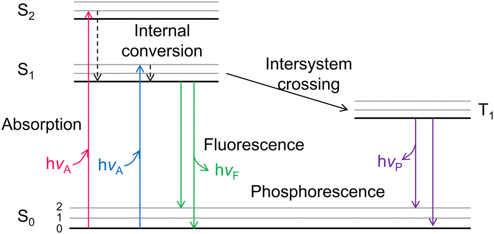 | ||
| Fig. 2 Jablonski energy band diagram. S0: ground state orbital, S1: the first excited singlet state, S2: the second excited singlet state, hvA: absorbed photon energy, hvF: energy released in the form of fluorescence. | ||
Steady-state PL spectroscopy mainly studies the fluorescence signal of photocatalysts under continuous light source irradiation. In steady-state spectra, the detection of fluorescence signal/intensity (y-axis) is a function of wavelength (x-axis). The steady-state light source is generally a xenon lamp with continuous spectral and energy output. The lower the peak intensity, the more significantly the radiative recombination of charge carriers is suppressed. To improve the photocatalytic H2 generation ability of pure g-C3N4, Yu et al.99 designed a novel graphdiyne (GD)/g-C3N4 hybrid nanocomposites (Fig. 3a). To unveil the mechanism for boosted H2 generation ability over GD/g-C3N4, PL spectra of pure g-C3N4 and GD/g-C3N4 composite were performed at room temperature and an excitation wavelength of 365 nm (Fig. 3b). It was worth note that compared to g-C3N4, the peak intensity at around 430 nm significantly decreased in GD/g-C3N4, indicating its inhibited electron–hole recombination. The formation of interfacial C–N bond during the heat treatment not only increased the electron density, but served as carrier transfer channel for fast electron transfer from g-C3N4 to GD, benefiting the carrier separation. Thus, the optimized 0.5% GD/g-C3N4 yields a maximum H2 evolution rate of 39.6 μmol h−1, 6.7 times higher than that of pure g-C3N4. The steady state PL technology was commonly used to qualitatively analyze the radiative recombination of carriers.
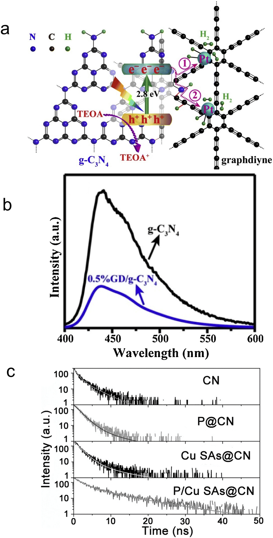 | ||
| Fig. 3 (a) Schematic diagram for photocatalytic H2 evolution on graphdiyne/g-C3N4 hybrid nanocomposite. (b) Steady-state PL spectra of the samples. Reproduced with permission.99 Copyright 2019, Elsevier B.V. (c) TRPL analysis and fitting results (λex = 320 nm). Reproduced with permission.101 Copyright 2022, Wiley-VCH. | ||
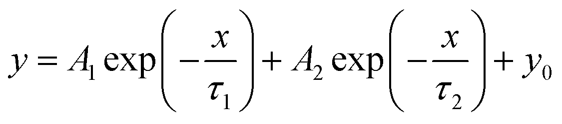
Time-resolved PL (TRPL) spectra was known as transient fluorescence analysis technique, providing in-depth information about carrier lifetime in semiconductor materials.100 When the light source stopped irradiating, the emitted fluorescence did not disappear immediately, but gradually decayed and finally vanished. In time-resolved spectra, the detected fluorescence signal/intensity (y-axis) is a function of time (x-axis). The time window can range from picoseconds (ps) to milliseconds (ms) and beyond. Usually, the fluorescence lifetime was the minority carrier lifetime (holes in n-type and electrons in p-type materials), which refers to the carriers from generation to disappearance. By irradiating the sample with pulsed monochromatic light (the wavelength of the monochromatic light is the peak wavelength in the PL spectrum), the dynamic process of the excited state radiation transition spectrum of the photocatalyst over time is obtained. The longer the fluorescence lifetime, the longer travel distances of the electron–hole pairs, and thus the higher carrier separation efficiency. The TRPL results are fitted by a binary exponential decay function model:

To achieve a superior photocatalytic C2H6 evolution rate, Mao and coworkers anchored P and Cu dual sites into graphitic carbon nitride (CN).101 To understand the highly efficient carrier transfer on the optimized P/Cu SAs@CN, TRPL spectra of the as-prepared samples were carried out (Fig. 3c). Through exponential decay function fitting, the average lifetime (τave) of CN, P@CN, Cu SAs@CN, and P/Cu SAs@CN were calculated to be 2.47, 2.56, 2.84, and 7.13 ns, respectively. The quasi-in situ XPS measurement exhibited positive shift of P 2p orbit and negative shift of Cu 2p orbit after light irradiation upon P/Cu SAs@CN, suggesting that the dopant Cu and P acted as electron and hole capture sites respectively, to achieve superior spatial separation of the carriers in CN. The carrier lifetime of the optimized P/Cu SAs@CN is 2.9 times of pure CN, triggering C2H6 product selectivity of 33% and high C2H6 evolution rate of 616.6 μmol g−1 h−1 (about 26 times higher than that of Cu SAs@CN counterpart). In addition to photocatalytic half reaction, the effective separation of photo-generated electron and holes are also key to the overall water splitting. Yang et al.102 presented an electron–hole rich dual-site nickel-based catalytic systems, which was a composite of Ni2P, NiS, and polymeric carbon–oxygen semiconductor (named Ni2P/NiS@PCOS) for robust overall water splitting. Through TRPL measurement, the average lifetime of Ni2P/NiS@PCOS was 9.74 ns, much higher than the pristine counterparts. This promoted carrier separation was ascribed to the nano-size heterojunctions between Ni2P and NiS. The optimized photocatalyst achieved superior performance of 150.7 μmol h−1 H2 and 70.2 μmol h−1 O2 per 100 mg photocatalyst, with stoichiometric 2:1 hydrogen to oxygen ratio in a neutral solution. Also, it displayed the AQE of 7% at 420 nm and high STH of 0.91%. A longer carrier lifetime indicated that the photo-generated electrons and holes require a longer time to complete the energy relaxation process. More carriers can transfer across the bulk material and reach the surface for catalytic reaction, to benefit the catalytic performance.
Due to the Coulomb interactions between the negatively charged photoelectrons and positively charged holes, they are easily attracted to each other and joined together to form excitons.103,104 Excitons were a bound state system formed by the interaction between electrons and holes. The exciton binding energy (Eb) is shown in Fig. 4a, representing the energy required for exciton dissociation to form free electrons and holes. The smaller the Eb, the larger the energy difference between electrons and holes to inhibit carrier recombination. Since the Eb of a semiconductor was closely related to the energy band structure, the exact Eb value can be directly obtained through temperature-dependent photoluminescence (TDPL) spectroscopy. When increasing temperature within PL test, the energy band structure of the semiconductor varied a lot, leading to increased Eb and quenched PL intensity. Thus, the linear relationship between the temperature and Eb can be obtained within a certain temperature range.
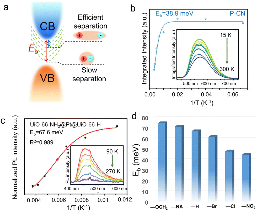 | ||
| Fig. 4 (a) Schematic illustration showing the exciton states with different Eb values of the semiconductors. (b) Integrated PL emission intensity as a function of temperature (inset: TDPL spectra) of P-2CN. Reproduced with permission.107 Copyright 2023, Wiley-VCH. (c) Integrated PL emission intensity of UiO-66-NH2@Pt@UiO-66-H as a function of reciprocal temperature (inset: temperature-dependent PL spectra from 90 to 270 K, with the excitation wavelength of 380 nm). (d) The Eb values of UiO-66-NH2@Pt@UiO-66-X with different ligand groups. (c) and (d) Reproduced with permission.84 Copyright 2023, Wiley-VCH. | ||
Owing to the low dielectric constant of organic semiconductors, the photo-exited electrons and holes were easily bound to form excitons within band gap.81,82 Generally speaking, excitons are unstable species. Excitons may have the following possible modes of action: energy transfer or energy decay. Excitons experience energy loss every time they leap or vibrate, and the process can be either radiative or non-radiative decay, which is unfavorable for photocatalytic processes that require effective carrier separation. Exciton binding energy and lifetime are the two most important parameters which controlled exciton dynamics, and it is generally believed that they are positively correlated.105,106 Therefore, it is necessary to adjust the exciton binding energy of semiconductor materials and convert it into free electrons and holes as much as possible before the exciton energy decays completely (that is, reducing the binding energy to dissociate excitons), for desirable photocatalytic application which required efficient carrier separation. Wang et al.107 rationally designed three conjugated polymers (CP) with a more delocalized electronic transmission channel and planar molecular structure, to accelerate the internal charge transfer process. TDPL technique was used to quantify the Eb values of the CPs (Fig. 4b). After fitting the data by the Arrhenius equation:
Jiang et al.84 fabricated a series of sandwich-structured metal–organic framework (MOF) composites, UiO-66-NH2@Pt@UiO-66-X (X = –H, –Br, –NA, –OCH3, –Cl, –NO2), for photocatalytic H2 production. With decreased temperature from 270 to 90 K, the PL intensities of NH2@Pt@UiO-66-X at around 460 nm increased monotonically, which can be further fitted to quantify the values of Eb (Fig. 4c). Accordingly, the calculated Eb values followed the sequence of –OCH3 (75.2 meV) > –NA (71.9 meV) > –H (67.6 meV) > –Br (62.1 meV) > –Cl (48.4 meV) > –NO2 (45.3 meV), suggesting the highest charge separation efficiency of UiO-66-NH2@Pt@UiO-66-NO2 sample (Fig. 4d). The promoted carrier separation can be ascribed to superior electron-withdrawing degree of –NO2 group. As a result, the exciton lifetime of UiO-66-NH2@Pt@UiO-66-X decreased significantly from 120 ps of –NA to 33.7 ps of the optimized —NO2. Han et al.108 developed a series of stable multifunctional lead-free halide perovskites (Cs2PtxSn1−xCl6 (0 ≤ x ≤ 1)), which showed varied photocatalytic functions by varying the amount of Pt4+ substitution. With the Pt content increased from 0 to 1, the efficient self-trapping induced enhanced radiative transition process, leading to significantly decreased Eb values from 572 to 140 mV. Pt-substitution forming Cs2PtxSn1−xCl6 solid solutions was confirmed to be an effective approach to tune the radiative recombination process.
In addition to organic semiconductors, TDPL method was also utilized for inorganic systems such as oxides and sulfides.109,110 By conducting TDPL test and fitting the relationship between characteristic peak intensity and the reciprocal of temperature, the exciton binding energies of different material systems can be obtained. The reduction of exciton binding energy can effectively regulate the lifetime of excitons and free carriers, which benefited carrier transfer dynamics and photocatalytic performance. This technology can reveal how various modification methods affect the carrier separation kinetics in low dielectric constant semiconductors from the intrinsic physical properties, thereby achieving high photo-assisted catalytic activity.
3.2. Transient absorption techniques
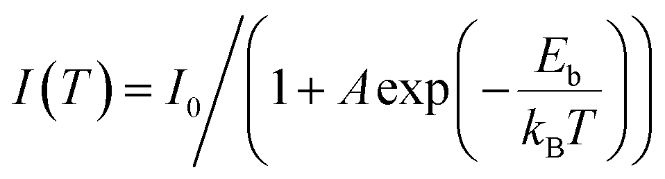
As a well-known “pump–probe” technique, transient absorption spectroscopy (TAS) was a powerful tool for studying the relaxation process of excited states in processes of luminescence and non-radiative recombination.111,112 The “pump–probe” referred to a technology that used optical pump pulses to excite the sample to the excited state, and then monitored the relaxation process of returning to the ground state using probe pulses (Fig. 5a).113,114 Like TRPL, TAS can also quantify the carrier lifetime to investigate carrier transfer dynamics, and it monitors the excited state absorption changes rather than the recombination process (for TRPL). The signal comes from the absorption or bleaching of probe light by excited state carriers. Typically, the main components of the system included a femtosecond laser amplifier with the wavelength of 800 nm, an optical parametric amplifier, an optical delay device, and the transient spectrometer to detect the signal (Fig. 5b). The pump pulse generated by optical parametric amplifier is monochromatic light in the wavelength from 240 to 2400 nm, the probe pulse is the white light at 250–850 depending on the nonlinear crystals and filters, and the data collection system will also receive the trigger signal from the 800 nm laser source. The time resolution was essentially determined by the pulse width of the laser, which ranged from hundreds of kilohertz to terahertz. So far, the shortest pulse width can even reach attoseconds. For the current utilized ultrafast fs-TAS, the abscissa was the relative value of the probe light. While, the ordinate ΔA represented the difference between the absorption spectra measured when the probe light is irradiated onto the samples with (A(λ)) and without (A0(λ)) the pump light, which reflected the change in the absorption ability of the probe light by the excited states of the sample under the pump light.50 In general, the obtained ΔA can be derived from the following four physical phenomena (Fig. 6): ground state bleaching (ΔA < 0), stimulated emission (ΔA < 0), absorption of excited states (ΔA > 0), and absorption of photoproduct (ΔA > 0). Since the TAS technique involves the data changes of both relaxation time and wavelength range, the spectra can be analyzed from two perspectives. On one hand, the TAS spectra can be acquired by detecting the light absorption of a certain transient substance. On the other hand, monitoring the changes of the transient substances at a specific wavelength can obtain the relationship between the absorbance and relaxation time. Regarding the delay time which represented the time difference between the pump pulse and probe pulse, the resolution can reach picoseconds and even femtoseconds, and the relaxation time can be obtained by fitting the curve. Fs-TAS can reveal the full lifecycle behavior of photo-generated carriers (including migration and recombination), particularly adept at analyzing ultrafast processes.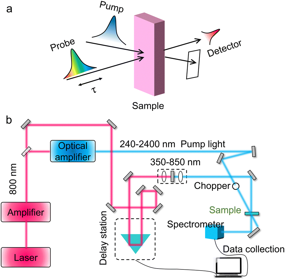 | ||
| Fig. 5 Schematic for the working principle of (a) probe–pump technique and (b) fs-TAS equipment. | ||
 | ||
| Fig. 6 Schematic diagram for different signals observed in fs-TAS method. | ||
Many research works have successfully monitored the interfacial carrier transfer dynamics in composite photocatalyts using the advanced femtosecond TAS (fs-TAS). Zhu et al.115 designed a 0D/1D heterojunctions of CdS quantum dots (QDs)/TiO2 nanotube arrays (CT) for photocatalytic dye degradation and hydrogen evolution. Compared with pure CdS QDs and TiO2 nanotube, the optimized heterojunction showed highest reduction of RhB concentration by 52% after 1 h, while the H2 evolution rate reached 46 μmol h−1. To better probe the underlying mechanism of the competition between the electron trapping, electron transfer and recombination in the composite CT sample, fs-TAS of the samples were performed (Fig. 7a). Different from the carrier transportation characteristics in traditional Type-II heterojunction, the electrons from the CB of TiO2 would recombine with the remaining holes in the VB of CdS, owing to the work function difference induced internal electric field between CdS and TiO2. The kinetics at 642 nm for the CT sample were fitted by a tri-exponential function with time constants of 1.2 ps (32%), 73.2 ps (41%) and 622.6 ps (27%). This suggested that the decoration of CdS QDs on TiO2 surface significantly accelerated the electron trapping process in the heterostructure within 1.2 ps, and prolonged the holes’ lifetimes which consumed by both shallow trapped electrons and deep trapped electrons. Through in-depth fs-TAS analysis, the essence behind the promoted photocatalytic performance over CT sample was clearly unveiled.
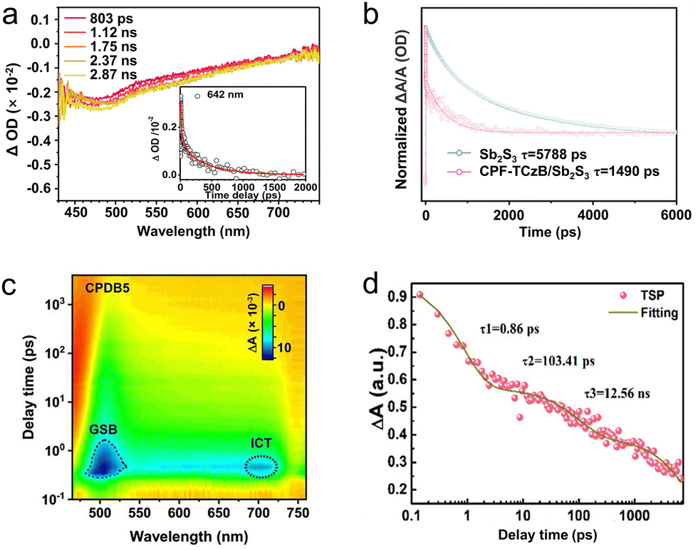 | ||
| Fig. 7 (a) Fs-TAS of CT-50 sample achieved after a 267 nm excitation in MeCN. Reproduced with permission.115 Copyright 2020, Elsevier B.V. (b) TAS kinetic traces and corresponding global fitting results of the Sb2S3 and CPF-TCzB/Sb2S3 photoanodes. Reproduced with permission.116 Copyright 2022, Wiley-VCH. (c) 2D mapping TA spectra of CPDB5 sample. Reproduced with permission.119 Copyright 2023, Wiley-VCH. (d) Time profiles of normalized transient absorption for TSP catalyst after 400 nm laser pulse irradiation. Reproduced with permission.120 Copyright 2023, Wiley-VCH. | ||
To inhibit the photocorrosion of Sb2S3 photocathode, Xu et al.116 designed a transparent Sb2S3-based photoanode, through depositing a thin conjugated polycarbazole frameworks (CPF-TCzB) layer onto the Sb2S3 film, for robust PEC H2 evolution. In addition to the traditional PL measurement, TAS was further applied to elucidate the role of the created heterojunction in manipulating charge transfer dynamics. The TAS of Sb2S3 and CPFTCzB/Sb2S3 featured a prominent photo-induced absorption peak within 450–600 nm (Fig. 7b), which typically arise from the formation of trapped holes or the hole-induced sulfur radicals in Sb2S3. Accordingly, The photo-generated holes in CPF-TCzB/Sb2S3 exhibit a strikingly shorter carrier lifetime (≈1490 ps) than those in Sb2S3 (≈5788 ps), indicating that the photo-generated holes in Sb2S3 can transiently transferred across the heterojunction, thereby significantly improving the charge separation efficiency.117,118 In addition, a broad peak between 600 and 700 nm, which was attributed to the absorption of photo-induced electrons, can be observed in the TAS of the CPF-TCzB photoanode, while not observed in that of CPF-TCzB/Sb2S3. This implied that the photo-generated electrons in the CPF-TCzB can be rapidly consumed by the holes extracted from the Sb2S3. The CPF-TCzB/Sb2S3 hybrid photoanode exhibited a superior photocurrent density of 10.1 mA cm−2 at 1.23 V vs. RHE in 1 M PBS electrolyte, with a high ABPE of 3.35% at 0.7 V vs. RHE and an excellent long-term stability for >100 h.
TAS technique was also successfully applied in probing carrier transfer in the novel S-scheme heterojunctions. Yu et al.119 constructed a series of CdS/pyrene-alt-difluorinated benzothiadiazole (PDB) S-scheme heterojunction, and unveiled the photophysical process of the structure using fs-TAS (Fig. 7c). The TAS of pure CdS indicated three electron-relaxation pathways, including diffusion over lattices, electron–hole pairs recombination, and the recombination of photo-generated electrons and trapped holes. After PDB decoration, an additional interfacial charge-transfer signal can be detected in the spectra of heterojunction, and the corresponding electron transfer lifetime was 78.6 ps. Ascribing to the accelerated interfacial charge transfer, the optimized photocatalyst exhibited higher photocatalytic H2 production rate of 7.14 mmol h−1 g−1 and 1-phenyl-1,2-ethanediol conversion efficiency of 98% than that of pure CdS (H2 evolution rate of 1.15 mmol h−1 g−1 and 1-phenyl-1,2-ethanediol conversion efficiency of 17%). To avoid futile carrier transfer routes in series S-scheme photocatalysts, Cui et al.120 proposed a twin S-scheme heterojunction system, in which the hydrogen-doped rutile TiO2 nanorods (H-TiO2) and anatase TiO2 nanoparticles (a-TiO2) were successfully self-assembled on graphitic C3N4 (CN) nanosheets. Fs-TAS was measured to investigate the transportation dynamics of twin S-scheme catalyst (donated as TSP). Compared with the pure CN, H-TiO2, and a-TiO2 counterparts (Fig. 7d), the as-prepared TSP exhibited fast trapping electrons and slow recombination rates of the photo-generated carriers. More photo-excited electrons can be captured by the trap states, contributing to the improved carrier separation and transfer efficiency. As a result, TSP exhibited the highest total τ value (5105.2 ps), indicating the longest carrier lifetime. The optimized catalyst showed an excellent photocatalytic hydrogen evolution rate of 62.37 mmol g−1 h−1, far exceeding those of the counterparts. The apparent quantum efficiency (AQE) of the system reached 45.9% at the wavelength of 365 nm and the performance can be maintained for over 20 h, ascribing to the promoted carrier separation.
In addition, the role of defects can be monitored by fs-TAS technique. During the preparation of nanomaterials, intrinsic defects are inevitably introduced. These defects can either act as recombination center or as charge trapping sites to facilitate the carrier separation, thus the characterization for unveiling the role is of great significance. Wei et al.121 well designed a VO–WO3–Pt system for photocatalytic oxygen evolution reaction. Through fs-TAS spectra, the introduction of VOs prolonged the longer lifetime components from 441.7 to 749.1 ps, revealing that the VO acted as the electron-trapping sites favored the electron–hole separation. Ruan et al.122 investigated the role of N defects in g-C3N4 for photocatalytic H2 evolution. Different from pure C3N4, the presence of N defects led to negative TA signals in the visible probe region, suggesting that the N defects introduced shallow trap sites to capture electrons, to accelerate the carrier separation. By analyzing the changes in the shape of the TAS spectra, combined with fitting the decay curve of fs-TAS spectra with appropriate model to index the lifetime component of charge trapping, the role of defects in photocatalysts can be revealed effectively.
Different from TAS technique which usually monitored the behavior of deep-trapped charges, time-resolved infrared (TRIR) spectroscopy traced transient changes in the IR spectrum, making TRIR more sensitive to free and shallow-trapped carriers.123 The configuration of the TRIR spectrometer for kinetic measurements on photocatalysts were shown in Fig. 8.124 Two external cavity tunable quantum cascade lasers (QCL) were utilized in continuous wave mode to provide monochromatic emission. The emitted IR irradiation was directed to an adjustable aperture, and then the beam was focused onto a photovoltaic mercury cadmium telluride (MCT) detector by means of three mirrors. After the signal treatment through preamp, the recorded data were merged to yield a trace from nanoseconds to hundreds of milliseconds.
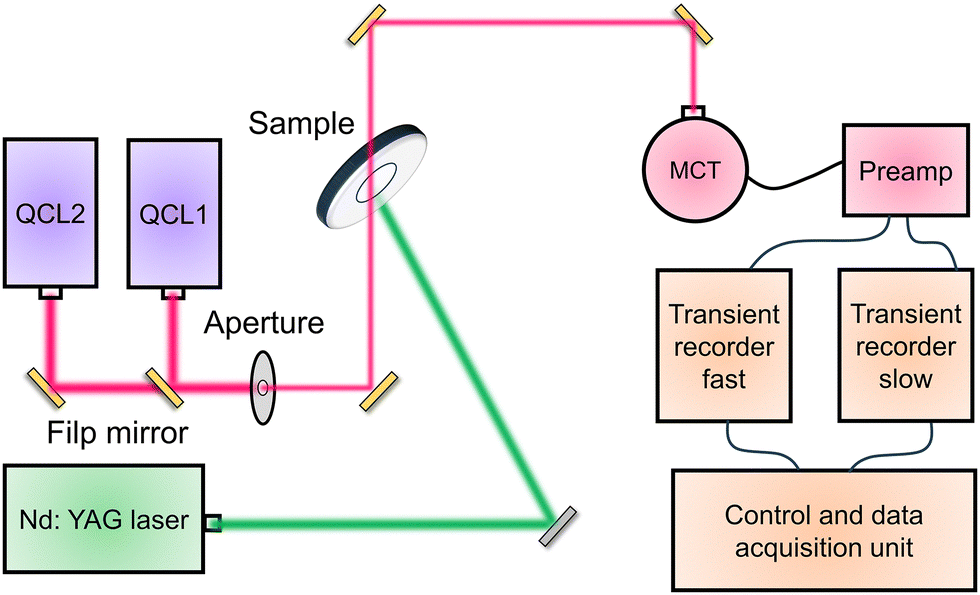 | ||
| Fig. 8 The diagram of the TRIR absorption spectrometer for kinetic measurements on photocatalysts. QCL: tunable quantum cascade lasers. MCT: mercury cadmium telluride detector. | ||
Semiconductor–nanometal structure had been recognized as efficient heterojunction to facilitate the interfacial separation of photo-generated carriers, while, the carrier transfer direction remained elusive. To directly explore the promoted photocatalytic mechanism and unveil the intrinsic properties of widely utilized TiO2/Au, Su et al.45 monitored the decay kinetics of photo-induced electrons upon UV and vis excitation by nanosecond TRIR technique, which offered observations without the influence of holes. Under UV excitation (355 nm laser), both pure TiO2 and TiO2/Au samples exhibited fast decay in 1 μs initially and then a slow decay within 250 μs. As the slow decay component corresponded to the long-lived photoelectrons, the higher normalized decay of TiO2/Au suggested promoted carrier separation. Under 532 nm irradiation (Fig. 9), the detected long-lived electrons can be due to the electron injection from the excited states of Au to the CB of TiO2. In addition to the traditional TiO2/Au structure, Wang et al. studied the dynamics of photoelectrons in Ga2O3 loaded with Cr2O3–Rh cocatalyst by TRIR.125 After recording the decay plots of the four samples (Rh/Ga2O3, pure Ga2O3, Cr2O3/Ga2O3 and Cr2O3–Rh/Ga2O3) in different atmospheres (air, water vapor,vacuum etc.), they found that only the electrons trapped by Rh particles can efficiently participate the H2 evolution reaction (HER), in which the Cr2O3 promoted the electron transfer from Ga2O3 to Rh. Based on the synergistic promotion of Cr2O3 and Rh to photo-generated electron transport, the photocatalytic HER activity of the optimized Cr2O3–Rh/Ga2O3 was 18 times higher than that of pure Ga2O3.
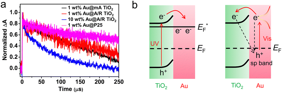 | ||
| Fig. 9 (a) Normalized decay curves of TRIR absorption at 1200 cm−1 for the photoelectrons in different Au/TiO2 photocatalysts upon the excitation wavelength of 532 nm. Reproduced with permission.45 Copyright 2019, American Chemical Society. (b) Schematic energy level diagram illustrating electron transfer and the recombination process under UV and Vis irradiation. | ||
Homojunction exhibited higher photocatalytic activity than that of pure phases, however, there existed contradictory opinions about the electron transfer direction between the two phases.126–131 To clarify the carrier migration, Li et al.132 performed the photo-induced electrons kinetics on anatase, rutile, and anatase-rutile mixed phase TiO2 under vacuum or methanol vapor using TRIR method. Through systematic investigation, they found the electrons transfer from the CB and shallow trap states of anatase to rutile within 50 ns after excitation, to prolong the carrier lifetimes and enhance the photocatalytic performance. Perovskite photocatalyts such as SrTiO3 and NaTaO3 were promising materials with the advantages of high dielectric constant, low dielectric loss, and good thermal stability,133,134 while severe carrier recombination limited their application. To address this challenge, Li et al.135 fabricated Cr-doped SrTiO3 for efficient photocatalytic H2 and O2 production. The decay of photo-generated carriers as a result of recombination and carrier reaction were traced by TRIR measurement. The time-resolved results revealed that the decay rate of photo-induced electrons with Cr3+ was slower than that with Cr6+, implying the superiority of Cr3+ for separating electrons and holes, and thus the enhanced photocatalytic H2 activity. Onish et al.136 examined the electron–hole recombination kinetics of perovskite NaTaO3 doped with Ca, Sr, Ba, and La using TRIR. Under light condition, the alkali earth elements doped NaTaO3 showed monotonous IR absorption, which was assigned to photo-excited electrons. Compared with pristine NaTaO3, the delayed times for electrons increased significantly with the order from La, Ca, Ba, to Sr, consistent with the trend for H2 production rates.
Briefly, the above discussions demonstrated the effectiveness of TRIR as a powerful technique for investigating the dynamics and behavior of photo-generated carriers in various materials and systems. This technique allowed researchers to gain insights into the fundamental processes that occur when light interacted with matter, such as charge separation, recombination, and transport on the timescale from femtoseconds to milliseconds. These were crucial for understanding and optimizing the performance of photovoltaic devices, photocatalysts, and other optoelectronic materials.137
3.3. Photoelectrochemical (PEC) methods
Through directly (in situ deposition) or indirectly (the photocatatlysts powder are prepared into slurry and performs ex situ coated) approaches, the photocatalysts can be loaded on conductive substrates, the separation process of photo-generated carriers can be monitored with the aid of electrochemical means under illumination. As PEC technique holds the similar basic principle with that of photocatalysis, it has gradually been accepted and used as an important auxiliary tool to study the carrier transport and separation under solar energy irradiation.138–140 Among various techniques, photoelectrochemical impedance spectroscopy (PEIS) is an important tool for studying carrier transfer within bulk and surface.141 The semiconductors were usually loaded on the conductive substrates such as FTO and ITO. There were various display methods for PEIS data, among which the most commonly used were the complex impedance plots (Nyquist plots) and Bode plots. The Nyquist plot consisted of the real part of the impedance as the horizontal axis and the negative imaginary part as the vertical axis, in which the circle radius can reflect the reaction resistance. For a typical Nyquist plot under illumination, two semicircles would appear in the high-frequency and low-frequency regions, respectively. The former represented the carrier transfer dynamics within the bulk semiconductor, and the latter can reflect the surface catalytic rates (Fig. 10a). Through selecting an appropriate equivalent circuit diagram to fit the Nyquist plot, the key parameters of external circuit resistance (Rs), bulk carrier transfer resistance (Rbulk), and surface carrier transfer resistance (Rct) can be obtained (Fig. 10b). The smaller the arc radius, the lower the transfer resistance of the photo-generated carriers, to achieve fast carrier separation.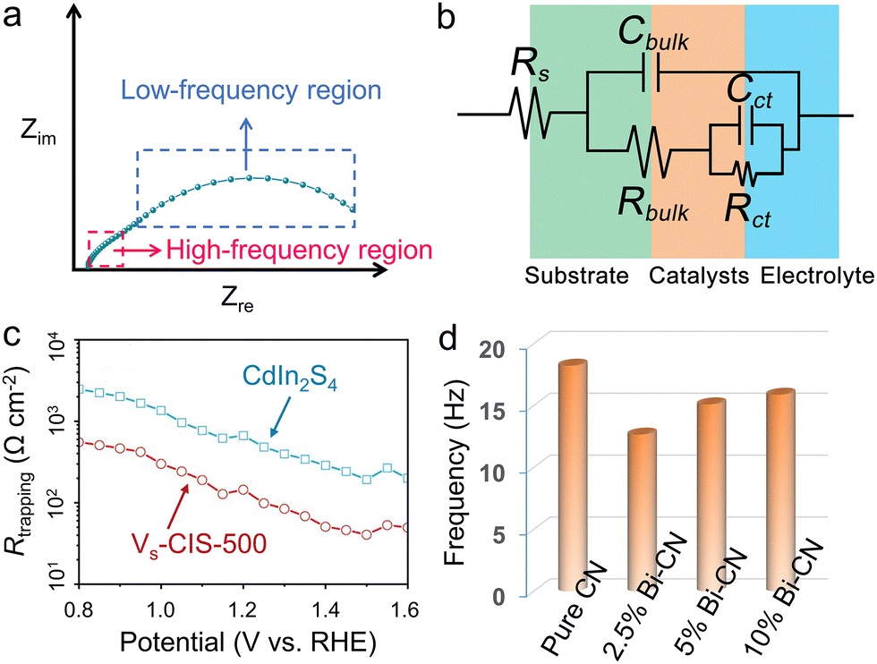 | ||
| Fig. 10 Schematic diagram for the (a) typical Nyquist plot and (b) equivalent circuit. (c) Fitted Rtrapping under different applied potentials that are extracted from the EIS results. Reproduced with permission.143 Copyright 2020, Springer Nature. (d) Bode-phase plots of the EIS spectra for pristine g-C3N4 and Bi-doped g-C3N4 hybrids. Reproduced with permission.148 Copyright 2020, Elsevier B.V. | ||
Yang and coworkers142 synthesized the first phosphorene–fullerene hybrid featuring fullerene surface bonding via P–C bonds, to boost photocatalytic HER performance. To unravel the effect of C60 decoration on the carrier separation dynamics, they performed the PEIS measurement in 0.5 M Na2SO4 solution, in which the photocatalysts were dispersed in isopropanol mixed with Nafion, and the slurry was spin-coated onto FTO glass for test. The smaller arc radius of BPNS-s-C60 hybrid than pristine BPNSs suggested a faster interfacial carrier migration of BPNS-s-C60, owing to theintramolecular charge transfer from BP to C60. Thus, the photocatalytic HER rate reached 1466 μmol h−1 g−1 on BPNS-s-C60 hybrid exhibited, 3.2 times of pure BPNSs. Intrinsic defects usually acted as trap states to capture free electrons or holes, thus to facilitate the carrier separation. Dai et al.143 employed the PEIS technique to incisively illustrate the changes of the resistances which corresponded to the charge trapping (Rtrapping) and transfer (Rct,trap) at surface states (SS) in CdIn2S4 (CIS) and CIS with sulfur vacancy (Vs-CIS) samples (Fig. 10c). By selecting appropriate physical equivalent model to fitting the Nyquist plots, the carrier transfer and carrier trapping process can be separated. The introduction of sulfur vacancies decreased the Rtrapping and Rct,trap, significantly decreased the carrier recombination. Thus, the carrier lifetime of Vs-CIS (40.67 ns) is about 2.0 times than that of pure CIS (21.78 ns). Ascribing to the sulfur vacancy, the photocurrent density of Vs-CIS (5.73 mA cm−2 at 1.23 V vs. RHE) was 6 times than that of pure CIS, with an applied bias photon-to-current efficiency (ABPE) of 2.49%.
In addition to the carrier transfer resistance, the fitted capacitance can also provide key information about the carrier transfer within bulk catalyst and catalyst/solution interface. As capacitance is a physical quantity that describes the ability of charge storage, under illumination, the fitted value of capacitance can reflect the accumulation of photo-generated carriers within different regions. Specifically, for bulk catalyst region, a decreased capacitance (Cbulk) was ideal, which implied a fast separation efficiency for the photo-generated holes and electrons in the photocatalyst.144 Under this condition, the bulk carrier recombination should be highly inhibited. While, the capacitance value at the catalyst/solution interface depended on the operation condition. Under open circuit condition, a high fitted capacitance (Cct) was desirable, which indicated that more photo-generated carriers had reached the surface to participate in the photocatalytic reaction.4 Under applied bias, a low Cct was preferable which reflected fast interaction between the surface photocarriers and reactants.
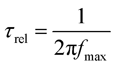
Bode plots can provide the information about the relaxation time (τrel) required for the photo-excited carriers migrating from the electrode surface to the electrolyte.145 The relaxation time was calculated from the following equation:
Besides the widely utilized PEIS technique, scanning electrochemical microscopy (SECM) has been recognized as a robust in situ tool to probe the carrier transfer kinetics at various interfaces, including solid–liquid and liquid–liquid interfaces.149,150 It was a scanning probe microscopy technique that used a nanometer or micron scale electrode as a probe. The micro-region morphology and chemical reaction information on the surface can be obtained by recording the Faraday current of oxidation or reduction reaction of molecular ions in the electrolyte solution around the probe, or other electrochemical parameters. In 2006, Wittstock et al.151 had successfully utilized SECM for investigating the dye regeneration (hole-involved process) kinetics in dye-sensitized solar cell (DSC) between I− and photo-oxidized dye molecules (Eosin Y+) adsorbed on ZnO. Then, Shen et al. extended this technique to investigate dye regeneration and the back transfer behavior (electron-involved process) at the photoanode/electrolyte interface after photoexcitation.152–154 According to the similarity of photoelectrochemistry with DSC, scanning photoelectrochemical microscopy (SPECM) may also be suitable to monitor the interfacial charge transfer kinetics in photo(electro)catalytic water splitting under working condition.
Typical SPECM device consisted the following four parts: electrochemical cell, solar light source, electrochemical workstation, and the data aquisition system (computer). Compared with traditional three-electrode system, the utilization of ultramicroelectrode (UME) or nanoelectrode as another working electrode to construct four-electrode system could scan across the sample surface to obtain surface morphological and local activity images simultaneously (Fig. 11). Under illumination, electrons and holes were generated in the photoelectrode, and reacted with the probe molecules in the electrolyte. As the faradaic current at the tip (iT) varied with the separation distance (d) between the tip and the substrate, the relationship curve can be defined as an approach curve (iTvs. d plot). The kinetics information including diffusion processes and steady-state processes would be extracted from such approach curve.
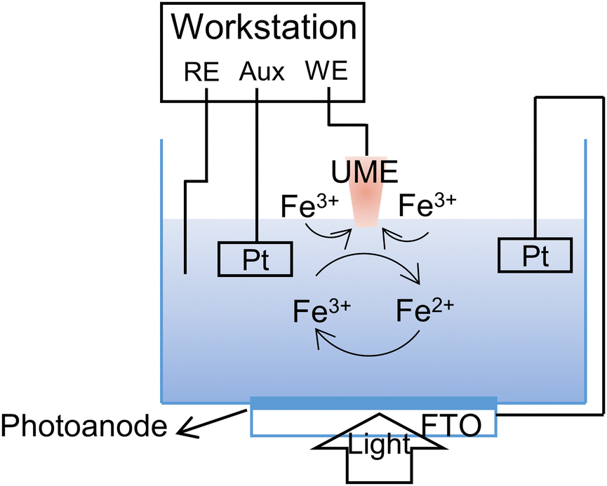 | ||
| Fig. 11 Basic principles for investigating the interfacial reaction kinetics in photoelectrochemical water splitting under the feedback mode of SPECM. | ||
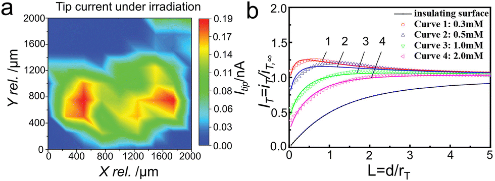
In 2016, Conzuelo and coworkers155 performed the SPECM surface scans in the analysis of a PS1/redox hydrogel spot deposited on a Si wafer (Fig. 12a). Specifically, the microelectrode tip was used both as electrochemical probe and as source for irradiation, to accomplish the local illumination of the samples. Through SPECM surface scans, they found that carrier severely recombinated when Au was used as electrode material. While, by using p-doped Si as electrode material, the emergence of short-circuiting confirmed the impeded recombination process. Wittstock's group156 studied the charge transfer kinetics and carrier recombination process of photogenerated holes in the BiVO4/NiFe-LDH system through the feedback mode of scanning electrochemical microscopy (Fig. 12b). In order to guarantee the electron transfer between substrate and Pt ultramicroelectrode to constitute a loop, the redox mediator of [Fe(CN)6]4− and [Fe(CN)6]3− (E0 = 0.45 V vs. Ag/AgCl) was selected as an excellent receptor for the photo-generated electrons and holes to investigate the kinetics for PEC water splitting. Under illumination, the ratio of rate constants for photo-generated hole (kh+) to electron (ke−) via the photocatalyst of BiVO4/NiFe-LDH reacting with the redox couple was 5 times higher than that of pure BiVO4. The results implied that the cocatalyst NiFe-LDH suppressed the electron back transfer greatly and finally reduces the surface recombination. A photocurrent density of 2 mA cm−2 at 1.23 V vs. RHE was achieved over BiVO4/NiFe-LDH, 4 times higher than that of pure BiVO4.
 | ||
| Fig. 12 (a) SECM surface scans recorded in the analysis of a PS1/redox hydrogel spot deposited on a Si wafer. Tip currents recorded under light. Reproduced with permission.155 Copyright 2017, Wiley-VCH. (b) Normalized SPECM approach curves in the feedback mode with the Pt ultramicroelectrode approaching BiVO4/NiFe-LDH film with different concentrations of the redox mediator [Fe(CN)6]3−, under illumination with a blue LED. Reproduced with permission.156 Copyright 2021, American Chemical Society. | ||
Interestingly, the investigated surface can be unbiased or decoupled from the electrochemical system, acting purely as a photocatalyst. The UME enables quantitative, spatially resolved detection of photoproducts, providing valuable insights into the solid–liquid charge transfer dynamics. To date, this remains the only technique that allows the direct detection of local photo-reacting species under operando conditions.157,158 In short, SPECM was proved to be increasingly powerful in photo- and photoelectro-catalysis, including carrier transfer kinetics quantification, intermediate species determination, and reaction active sites exploration, which can provide helpful information of the semiconductors under operating conditions at spatial and temporal scales.
Table 4 summarizes the calculated carrier lifetimes of different semiconductors (including oxides, sulfides, and organic systems etc.) through various time-resolved techniques (including TAS, TRPL, and PEIS). It is worth note that the time scale of carrier lifetime obtained by different characterization methods varies. Specifically, TAS can detect the transition routes and rates between excited state energy levels of samples in different states. One of its major features is that it can monitor the complete transition process of molecular excited states within a detectable delay time, especially femtosecond transient absorption, which provides ultrafast femtosecond and picosecond scale transition processes. Thus, the carrier time scale by TAS reaches ps or even fs level, making TAS a key tool for explaining photocatalytic phenomena and in-depth mechanisms. It can be extracted from the literatures that the photocatalytic activity of materials is often not positively correlated with the tested carrier lifetime, especially by fs-TAS and TRPL techniques which reflected the intrinsic property of the semiconductor systems. The carrier lifetimes are closely related to factors including the complexity of the material structure (single phase or composite), defect location (surface, interface, and bulk) and density, and modification methods.159–161 Therefore, it is necessary to combine the actual material system and structure to study the influence of changes in carrier lifetime on its separation efficiency and photocatalytic performance.
| Characterization methods | Material systems | Carrier lifetime | Ref. |
|---|---|---|---|
| TAS | Core–shell α/γ-Fe2O3/FCP | 50.64 ps | 164 |
| α/γ-Fe2O3 | 33.45 ps | ||
| α-Fe2O3 | 21 ps | ||
| VO–WO3–Pt | 163.6 ps | 121 | |
| VO–WO3 | 749.1 ps | ||
| WO3 | 441.7 ps | ||
| CdS@PDB | 1523.4 ps | 119 | |
| CdS | 1051.1 | ||
| SAs Pt: Fe2O3 | 486.76 ps | 92 | |
| NPs Pt/Fe2O3 | 437.28 ps | ||
| g-CN/S-20 | 565.8 ps | 165 | |
| g-CN | 129.6 ps | ||
| In2O3-cube/g-C3N4 | 192.8 ps | 166 | |
| PUCN | 163.3 ps | ||
| WO3–VO/In2S3 | 528.1 ps | 167 | |
| WO3–VO | 194.4 ps | ||
| TRPL | W18O49@CdS nanotubes | 14.25 ns | 168 |
| W18O49 | 4.81 ns | ||
| SnS2/g-C3N4 | 6.52 ns | 169 | |
| g-C3N4 | 6.01 ns | ||
| BiVO4/BiOBr | 3.39 ns | 170 | |
| BiOBR | 1.74 ns | ||
| CsPbBr1.95Cl1.05 | 3.28 ns | 171 | |
| CsPbBr1.65Cl1.35 | 1.53 ns | ||
| Cu–In–Zn–S/Ni-MOF | 59.24 ns | 172 | |
| Cu–In–Zn–S | 30.92 ns | ||
| Pt/C3Nx | 8.34 ns | 173 | |
| C3Nx | 6.58 ns | ||
| SrTiO3@2Mo2C | 3.21 ns | 174 | |
| SrTiO3 | 2.06 ns | ||
| PEIS | NCO@CC with TiO2 ETL | 3.5 ms | 175 |
| NCO@CC | 0.4 ms | ||
| α-Fe2O3/g-C3N4 | 4.2 ms | 176 | |
| α-Fe2O3 | 2.9 ms | ||
| g-C3N4 | 1.9 ms | ||
| Crystal facet-modulated BiVO4 | 40.82 ms | 177 | |
| Pure BiVO4 | 1.38 ms | ||
| Cu–N–C@SnS2 | 0.76 ms | 178 | |
| SnS2 | 0.26 ms | ||
| Fe2O3/CdS/Co–Pi | 15.7 ms | 179 | |
| Fe2O3/CdS | 9.4 ms | ||
| Fe2O3 nanorods | 4.9 ms | ||
| Fe2O3@ZIF-67 | 2.8 ms | 146 | |
| Pure Fe2O3 | 1.46 ms | ||
Fs-TAS technology can generally detect dynamic processes at higher carrier concentrations. While, for the samples with low carrier concentration, there may be significant differences between the measured and the real carrier transfer kinetics, making the TAS results less reliable. Regarding the preparation process of the sample, fs-TAS can directly be performed for thin film and solution systems, while the powder photocatalysts should be spin coated or compressed on the quartz glass. In addition, for composite systems, the obtained spectral signal is often not a single absorption signal, but rather a superposition of multiple different signals. These signals include excited state absorption (ESA), ground state bleaching (GSB), and stimulated emission (SE). Therefore, data analysis is crucial for analyzing the dynamics of carrier transport. Different from the ultrafast TAS method, since the generation of fluorescence is the radiative recombination of excited electrons and holes, the time scale for most semiconductors is at the level of nanosecond using TRPL, in which the average carrier lifetime refers to that of minority carrier.162,163 By modifying the geometric, electronic, and band structures of the materials, the carrier separation efficiency within the bulk phase can be improved, effectively avoiding energy relaxation in the form of photons and thereby enhancing photocatalytic performance. The difference between fs-TAS and TRPL in testing carrier lifetime mainly stems from the differences in the measured physical processes and the energy transfer mechanisms involved. Fs-TAS focuses on the initial relaxation process of charge carriers in the excited state, resulting in shorter lifetimes (in the picosecond range). While, TRPL measures the radiative transition process of fluorescent substances from excited state to ground state, resulting in a longer lifetime (in the nanosecond range).
For photoelectrochemical catalysis, a certain external bias is often applied to the active semiconductor photoelectrode through the electrochemical workstation, to promote the carrier transfer within the bulk phase without the occurrence of side reactions. Thus, the carrier lifetimes for most typical semiconductors obtained from Bode plots are at millisecond level. Unlike TRPL and TAS tests which reflect the semiconductors’ intrinsic property, the PEIS technique can probe the carrier transfer dynamics under operating conditions (for instance, at 1.23 V vs. RHE for water oxidation reaction and at 0 V vs. RHE for water reduction reaction). The exponentially increased carrier lifetime indicates that the external electric field plays a crucial role in enhancing the transport of bulk carriers. By anchoring photocatalysts on transparent conductive substrates and applying electricity converted from renewable energy as the driving force, the photoelectrochemical process can compensate the shortage of low carrier separation efficiency in traditional photocatalytic application, to improve the solar-to-chemical energy conversion efficiency.
3.4. Transient photocurrent/photovoltage measurements
Taking n-type semiconductors as prototype, under illumination, the quasi-Fermi level of electrons tended to move upward which close to the CBM, while the quasi-Fermi level of holes shifted downward, generating an open-circuit photovoltage (Vph, Fig. 13a).180,181 The Vph value determined the driving force for the separation of surface electrons and holes, which can reflect the carrier transfer dynamics at the surface. By measuring the open circuit potential under continuous dark and light conditions, the Vph value of the semiconductor can be obtained.182 To reduce the interfacial energy loss and increase the Vph of BiVO4, Yang et al. demonstrated the work function adjustment via Mo doping (Fig. 13b).183 The optimal Mo content of 0.1% significantly reduced the surface TS and avoid the introduction of new states, leading to improved Vph and high carrier separation efficiency. The cliff-like junction within Mo-BiVO4 and B-C3N4 constructed a correct charge transfer channel, in which holes extracted from inner Mo-BiVO4 to outer B-C3N4, while the electrons migrated to the substrate and finally collected by the counter electrode. After modifying NiFeOx cocatalysts, the photoanode achieved photocurrent density of 5.93 mA cm−2 in PPB solution, with high ABPE of 2.67% and incident-photon-to-current conversion efficiency (IPCE) of 92%, respectively. In addition to Vph, transient photocurrent measurement was also a fundamental and widely utilized method for probing carrier transfer dynamics. The photoactive materials were commonly fixed on the FTO and ITO substrate, and the output photocurrent signals were collected under light illumination and applied bias in electrolyte. The photocurrent density represents the rate at which electrons and holes in photocatalysts oxidize or reduce the active species in electrolytes. Thus, a high photocurrent density of the semiconductor indicated that more photo-carriers can quickly migrate to the catalyst surface and participate in chemical reactions, reflecting fast carrier transfer dynamics. This technique is a qualitative approach to investigate carrier transfer dynamics.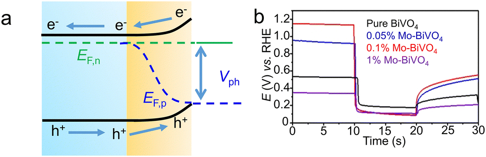 | ||
| Fig. 13 (a) Schematic diagram for the generation of Vph in typical n-type semiconductors. EF,n, quasi-Fermi level of electrons. EF,p, quasi-Fermi level of holes. (b) Vph of series BiVO4 samples after testing 30 seconds. Reproduced with permission.183 Copyright 2019, Springer Nature. | ||
Besides, intensity modulated photocurrent/photovoltage spectroscopy (IMPS/IMVS) was a spectroscopic technique that modulated the intensity of incident light and measured the resulting changes in photocurrent/photovoltage.5,184,185 Generally, the input signal contained a beam of stable background light and a beam of sinusoidally modulated light with small disturbance, while the output signal was the corresponded steady-state photocurrent/voltage with modulation.186 For example, Zhu et al.187 fabricated an oxygen-doped carbon nitride aerogel (OCNA) as the self-supported photocatalyst for efficient solar-to-hydrogen conversion. To investigate the structure–reactivity relationship, they utilized IMPS to evaluate the charge transport performance of bulk CN and series OCN samples. The transit time (τD) could be obtained by the equation of: τD = (2πfmax)−1, which represented the average time for the photo-induced electrons to reach the back substrate. fmax was the frequency corresponding to the minimum IMPS value. The τD of BCN of 22.4 ms was 10 times higher than that of OCNA (2.2 ms), demonstrating that OCNA possessed a much faster electron transfer rate and thus promoted the photocurrent density.
3.5. Space-charge limited current (SCLC) technique
When the semiconductors were excited under illumination, the photo-generated electrons and holes separated with each other and migrated from inner bulk to the surface for catalytic reaction. A key parameter that determined the carrier migration was the carrier mobility.188 As an intrinsic property of the semiconductor, it was the physical quantity that described the speed at which charge carriers moved in a semiconductor, defining as the average drift velocity of charge carriers per unit electric field strength (Fig. 14a). The carrier mobility was typically specified in unit of cm2 V−1 s−1, and its magnitude directly affects the conductivity of semiconductor materials. Thus, the value of the carrier mobility for electrons in the CB (μe) or holes in the VB (μh) was crucial to the photocatalytic performance of the materials. Since the carrier's velocity was equal to the mobility multiplied by the electric field intensity, the carrier's velocity was proportional to the mobility at the same electric field intensity. The higher the carrier mobility, the more distance it can travel within the bulk semiconductor in the same time, thus to accelerate the carrier transfer dynamics and achieve high carrier separation efficiency.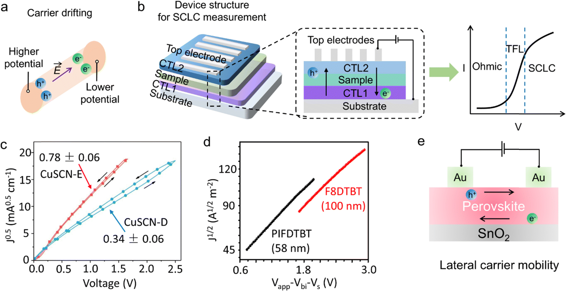 | ||
| Fig. 14 (a) Schematic diagram of drift motion of charge carriers under the driven of electric field. (b) Schematic diagram for the bulk mobility measurement based on the SCLC measurement with sandwich structure device. CTL: carrier transfer layer. TFL: trap-fill limit. (c) J0.5–V plots for CuSCN-based hole only devices.53 Copyright 2020, Springer Nature (d) the current density versus voltage characteristics of hole-only F8DTBT and PIFDTBT devices. Reproduced with permission.193 Copyright 2022, American Chemical Society. (e) Schematic illustration of device for the measurement of horizontal carrier mobility of 2D semiconductors. | ||
Accordingly, it was of great necessity to estimate the carrier mobility accurately. Among various reported approaches, the space charge-limited current (SCLC) method was one of the most common due to its apparent accessibility.189,190 The mechanism for carrier mobility measurement was as follows: in an ideal semiconductor over a particular range of applied voltage, the measured current density became limited by the space-charge formed by the charge carriers. When the speed of carrier movement slows down, the current density will reach a stable value. By measuring the current density–voltage (J–V) characteristics of the device at dark condition, the carrier mobility of semiconductor materials can be obtained by the Mott–Gurney equation of:
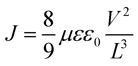
The SCLC technique was initially used for the carrier mobility calculation in the photovoltaic field. Recently, SCLC method was introduced to photocatalytic process for in-depth exploration of the carrier transfer kinetics. Similar to the solar cell, an electron/hole only device should be firstly constructed, in which the semiconductor was wrapped in a sandwich structure by the carrier transport layer (Fig. 14b).188,191,192 The construction of the device was as follows: first, the patterned ITO glass was as the transparent substrate, in which the surface impurities (organic compounds, oil film, and dust etc.) were cleaned by cleaning agents and alcohol under ultrasonic wave. Then, carrier transfer layer 1 (CTL 1), semiconductors, and carrier transfer layer 2 (CTL 2) were loaded on the ITO substrate sequentially. According to the type of the hole/electron transfer layer, the modification methods can be varied including sol–gel, sputtering, and evaporation etc. Finally, the top electrode (Ag or Al) was evaporated onto the CTL 2 through a shadow mask, to accomplish the fabrication of the device. During the measurement, bulk carrier mobility of the sample was obtained through J–V testing under the conditions of connecting the top electrode (usually Ag or Al) to the ITO substrate. For instance, Hagfeldt et al.53 presented a Cu2O photocathode for efficient solar water splitting performance, enabled by the modification of solution-processed CuSCN (electrodeposited with the aid of EDTA and DEA named CuSCN-E and CuSCN-D, respectively). To demonstrate the improved activity after CuSCN decoration, hole only devices with the structure of FTO/Au/CuSCN/MoO3/Ag were configured to determine the hole mobility of CuSCN (Fig. 14c). Au layer with the thickness of 100 nm was sputtered on top of FTO to block the electron injection under bias, while the MoO3 layer was acted as the hole transfer layer. In the trap-free SCLC regime, the current density was known to follow the Mott–Gurney law. By fitting the J–V plots, the μh of CuSCN-E and CuSCN-D were calculated to be 0.78 ± 0.06 and 0.34 ± 0.06 cm2 V−1 s−1, respectively. The excellent hole mobilities of CuSCN-E and CuSCN-D were favorable for extracting photo-excited holes in Cu2O to suppress the interfacial recombination. The band-tail states existence rendered a smooth hole transfer without overcoming the barrier (through VB), enabling fast interfacial carrier migration and superior water splitting performance. This PEC system delivered the photocurrent density of −6.4 mA cm−2 at 0 V vs. RHE, with a superior solar-to-hydrogen efficiency of 4.55%.
Li et al.194 prepared a completely [hk1] oriented Sb2S3 by sulfurizing a Ag/Sb bimetallic precursor film for photoelectrochemical water reduction. Mechanistic studies revealed that the improved carrier transport in Ag: Sb2S3, ascribing to the inhibition of the grain growth along the [hk0] direction, which contributed to a higher separation and injection efficiency of photo-generated carriers. Through configuring the Mo/Sb2S3/Au (Ti) structure for dark J–V measurement, the carrier mobility of Ag: Sb2S3 film ((6.13 ± 0.96) × 10−2 cm2 V−1 s−1) was ∼7 times higher than that of pure Sb2S3 film ((0.89 ± 0.67) × 10−2 cm2 V−1 s−1), ascribing to the Ag induced excellent intra-ribbon carrier transport of Sb2S3 film in the [hk1] orientation. As a result, a photocathode based on the [hk1]-oriented Sb2S3 film delivered a high photocurrent density of 9.4 mA cm−2 at 0 V vs. RHE and a high ABPE of 1.2% in a neutral electrolyte.
When selecting appropriate solvent (usually ethanol, ethylene glycol, isopropanol, and DMF) to configure uniformly dispersed solution, powder-based photocatalysts can also be loaded on the CTL 1 through stable spin-coating process, to construct reliable SCLC device. Chen et al.193 synthesized PIFDTBT polymer dots/g-C3N4 (CN) nanosheets for robust photocatalytic hydrogen evolution. To verify the high carrier mobility of the composite, the devices were fabricated with a ITO/PEDOT:PSS/Active layer/mMoO3/Ag structure in a glove box, in which the PIFDTBT was spin-coated onto the ITO/PEDOT:PSS substrate for SCLC measurement. Ascribing to the long effective chains and high planarity, the hole mobility of PIFDTBT reached 1.11 × 10⁻³ cm2 V−1 s−1, 6.5 times higher than that of F8DTBT counterpart (Fig. 14d). Thus, the HER performance of PIFDTBT/CN was 7.6 times higher compared to F8DTBT/CN. Likewise, Ray et al.195 reported CuS/carbon nanotubes (T-CuS) composite for photocatalytic RhB treatment, with a high degradation efficiency of 94% within 60 min. To probe the contribution of carbon nanotubes on the electron mobility, the SCLC device was fabricated with the structure of Al/CuS/ITO and Al/T-CuS/ITO. Specifically, the CuS and T-CuS were added into DMF solvent under ultra-sonication, and the well-dispersed medium was coated onto the glass substrate. The complex networks benefited the electron transfer of CuS, resulting in high electron mobility of T-CuS of 7.98 × 10⁻³ cm2 V−1 s−1, 3.4 times higher than that of pure CuS. In recent years, perovskite materials also exhibited superior photocatalytic performance. Satapathi et al.196 fabricated Cs2AgBiBr6-g-C3N4 heterojunction photocatalysts for CO2 reduction application, and utilized SCLC for electron mobility calculation. The structure of electron-only transport device was FTO/SnOTau/Perovskite/PCBM/Ag. The perovskite layer is prepared by dissolving the perovskite and its composites in DMSO at 100 °C, combined with spin-coating on FTO and annealing treatment. After C3N4 content optimization, the Cs2AgBiBr6–g-C3N4 composite exhibited a high electron mobility of 6.52 × 10⁻⁴ cm2 V−1 s−1, 27 times than that of pure Cs2AgBiBr6. Thus, a high average CO and CH4 yield of 12.14 and 8.85 μmol g−1 h−1 is achieved for Cs2AgBiBr6–g-C3N4. Besides, by connecting the two top electrodes which evaporated on the transport layer through a mask for J–V test (Fig. 14e), the carriers were forced to move laterally to acquire the horizontal carrier mobility of 2D semiconductors.197–199
In brief, SCLC method was a direct approach for obtaining the hole and electron's mobility of the semiconductors. Although this technology was currently widely used in the field of solar cells, the characterization of these intrinsic properties can help to provide in-depth evidences to illustrate the essence of the promoted carrier separation in powder-based photocatalytic process. This was exactly what traditional characterization means lacked. It should be noted that, to perform the SCLC more accurately, the sample layer in the configuration should be smooth and uniformly dispersed to guarantee the continuity of the circuit. This can be achieved by selecting proper solvent systems and finely controlling the operation and parameters of the spin-coating process.
The hole and electron mobility of typical photocatalysts (oxides, sulfides, perovskite structures, organic polymer etc.) are summarized in Table 5. In general, due to the strong binding of atomic nuclei to the holes on the VB, the effective mass of holes is much larger than that of free electrons. Thus, the hole mobility ranges from 10−4 to 10−2 cm2 V−1 s−1, which is several orders of magnitude lower than the mobility of electrons (from 10−1 to 102 cm2 V−1 s−1). The improvement of intrinsic poor hole mobility could be taken into consideration to design high-performance photocatalysts, and the well-accepted SCLC method plays the key role to evaluate the mobility regulation.
| Material systems | Carrier mobility (cm2 V−1 s−1) | Ref. |
|---|---|---|
| WO3/PEDOT:PSS | Hole: 1.35 × 10⁻³ | 200 |
| TiO2/P3HT | Hole: 3 × 10⁻⁴ | 201 |
| Al/rGO-TiO2 | Hole: 0.092 | 202 |
| Ti/CQD@α-Fe2O3 | Hole: 0.01 | 203 |
| spiro + SnS | Hole: 7.72 × 10⁻³ | 204 |
| m-CZTS | Hole: 5.5 × 10⁻³ | 205 |
| SnO2:InCl3 | Hole: 1.9 × 10⁻³ | 206 |
| ZnO | Electron: 100 | 207 |
| L15 film | Electron: 0.5 | 208 |
| PDI–PhCN | Electron: 0.212 | 209 |
| SnS2 | Electron: 0.17 | 210 |
| CsPbBr3/SrTiO3 | Electron: 518 | 211 |
3.6. Spatial resolved microscopy
In the past decades, time-resolved spectroscopy has been extensively applied to explore the carrier relaxation pathways, migration and recombination processes, and trapping behaviors, at different time scales from fs to μs. However, the laser's large penetration depth may simultaneously excite multiple carriers or defect states at different depths, resulting in complex spectral signals that were difficult to resolve. Meanwhile, it may cause thermal effects or light damage within the material, affecting the accuracy of the experimental results. Thus, the surface carrier transfer dynamics that were critical to the photocatalytic process may not be detected.Four-dimensional ultrafast electron microscopy (4D-UEM) was an advanced microscopy technology that combined ultrafast electron pulses with high-resolution imaging capabilities. It can conduct real-time, high-resolution observations of the dynamic processes of the materials in four dimensions (three dimensions plus time dimension), becoming one of the most important tools for revealing time-dependent phenomena in catalytic reactions at the femtosecond and nanometer scales (Fig. 15).212,213 In this method, a femtosecond laser pulse was used to excite the specific area of a sample, forming resolved image by detecting secondary electrons (SEs) emitted from the sample surface at different delay times. It has been reported that the observed image contrast was sensitive to the local electron/hole density change with respect to a reference image.214 Through 4D-UEM technique, the dynamics events of the observed signals can be acquired to obtain the temporal information on local charge density, which was conductive to understanding the effects of specific chemical components of catalysts on spatiotemporal information in photocatalytic reactions.
 | ||
| Fig. 15 Schematic of the experimental setup with the femtosecond laser integrated with SEM. HG: second harmonic generation. BS: beam splitter. L1: lens (12.5 cm). L2: lens (17.5 cm). | ||
In the field of photocatalysis, the ultrafast dynamical processes including carrier trapping and recombination on semiconductors surface occurred within nanometer and femtosecond scales. Mapping the surface dynamics selectivity in real time and space was an effective way to access such fundamental process to deeply unveil the migration behavior of charge carriers. Mohammed et al.215,216 established a second generation of 4D-UEM, whose spatiotemporal resolutions reached 5 nm and subpicosecond level (Fig. 16a). By utilizing 4D-UEM technique, the carrier migration, recombination, and trapping behaviors can be directly visualized. Taking silicon or CdSe single crystals as example, they found that the 515 nm optical pulse can induce the interband carrier transition within the materials, and the generated conduction band electrons were more likely to emit secondary electrons (SE), resulting in high recorded contrast due to the energy gain at the center of the excited region. In addition to CdSe, the carrier relaxation process in InGaN nanowires had also been studied by 4D-UEM. From different SEs images after excitation at 515 nm, the dark contrast can be observed at positive time delays, suggesting increased photo-generated electrons in the CB, although the scattering process still existed.
 | ||
| Fig. 16 (a) Conceptual scheme for scanning ultrafast electron microscopy (S-UEM). (b) A series of contrast images with the decay time ranging from 6.7 ps to 3.32 ns, in which the bright and dark contrasts correspond to the local density of electrons and holes respectively. Reproduced with permission.217 Copyright 2015, American Association for the Advancement of Science. | ||
In 2016, Zewail et al.217 utilized the 4D-UEM method to probe and image the carrier transfer process in p-type Si, n-type Si, and Si p–n junction. In pure n- and p-type Si samples, clear contrasts can be observed under 515 nm laser illumination. Compared with p-type Si, the contrast is relatively weak in n-type, suggesting a larger light absorption in high doping p-type semiconductor. With the decay time prolonged, the bright contrasts in both samples gradually disappeared. While, when combing the n- and p-type Si, the different contrast variation trend proved the carrier migration direction in p–n junction system (Fig. 16b). Specifically, after illumination for a short period of time (6.7 ps), the bright phenomena in both layers revealed the individual behaviors for n- and p-type silicon. With the decay time increased to 80 ps, bright and dark contrasts located above and below the layer, respectively, suggesting the directional migration and separation of electrons and holes, that is, electrons accumulated on n-type side while holes on p-type side. The brightest images for 80 ps also indicated the maximum density of excess carriers, decreased gradually and finally reached a plateau with the decay time of 3.2 ns. In a typical p–n junction composite material, the generation and transport of charge carriers can be clearly observed by 4D-UEM approach. These studies demonstrated the ability of 4D-UEM technique to unravel the spatiotemporal behavior of charge transport and recombination after excitation in intrinsic and heterogeneous semiconductors.
4D-UEM technique exhibited the potential to unveil the carrier transfer mechanism in both simple and complex structures under illumination, with ultrafast time resolution and nanometer-scale scanning capability. It can also predict the unexpected ballistic carrier velocity and the gated localization of carriers, which beyond the commonly recognized drift-diffusion model. It hold the merits of ultra-high speed imaging, high resolution, and non-invasiveness, providing a powerful tool for a deeper understanding of the internal carrier transport mechanism in semiconductors. However, the data generated by 4D-UEM technology was enormous and contained rich spatiotemporal information. Therefore, the process of data parsing and processing were relatively complex, requiring professional software and algorithm support, which demanded a high level of technical proficiency from professionals.
In recent years, the high-resolution kelvin probe force microscopy (KPFM) holds the ability to observe and measure the morphology, electrical properties, and other properties of material surfaces at the nanometer scale, providing a fresh avenue to directly image the localized carrier separation at the surface or within the interface of photocatalysts.33 In photocatalytic process, the photo-induced electrons and holes would migrate to different directions to cause the variation of the surface potential of the semiconductors, generating surface photovoltage (SPV). By detecting the capacitive electrostatic forces, the local contact potential difference (CPD) between AFM Probe and sample surface can be quantified (Fig. 17). Specifically, a microcantilever probe which highly sensitive to weak forces is used to gently contact the surface of photocatalyst samples. The potential difference between the probe and the sample surface induced the generation of electrostatic force. A lock-in amplifier was then used to detect this electrostatic force at the oscillation frequency w to obtain amplified CPD value. The electrostatic force can be precisely controlled to map and quantify the potential on the sample surface. The in depth analysis of the measured CPD data can obtain the SPV distribution and the work functions of the sample at nanometer resolution, to reveal the carrier separation, transfer, and recombination in the semiconductors.
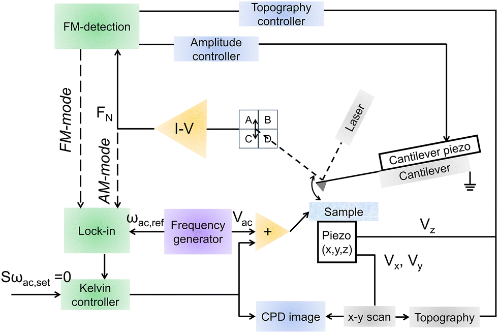 | ||
| Fig. 17 Signal detection principle for KPFM technique. | ||
Fig. 18a shows the SPV measurement with a conventional Kelvin probe on photocatalysts, which enabled the direct measurement of the light induced change of the CPD and thus the SPV of the catalyst. Li's group had made tremendous contributions in this field. For instance, they used light-irradiated KPFM to image photo-generated charge spatial distribution on an individual BiVO4 crystal under ambient conditions (Fig. 18b).218 Specifically, the CPD variation which termed SPV reflected the local charge density change on the sample surface induced by charge separation and transfer. Subsequently, they directly observed the directional separation of the electrons and holes to different specific facets on single BiVO4 particle. Under illumination, the brighter KPFM image indicated increased surface potentials, suggesting both {011} and {010} facets exhibited upward band bending in the space charge regions (SCRs). Thus, the photo-induced holes would preferentially transfer to the outer surface, while the electrons flow in the SCRs beneath the facets. After the photodeposition of MnOx and Pt cocatalyst on specific facets of BiVO4,219 the carrier transfer behavior changed a lot (Fig. 18c), and the SPV was ∼80 times higher than that of pristine BiVO4. Through SPV images, photo-generated electrons and holes were separated toward the {010} and {011} facets on the single BiVO4 particle, respectively. This confirmed that the reasonable modification of the cocatalyst benefited the formation of the additional built-in electric field, resulting in oriented charge transfer and separation. In addition, to understand the photo-induced carrier transfer feature at a homojunction interface, the surface potential distribution of anatase/rutile TiO2 composite system was imaged.220 The CPD difference between rutile and anatase suggested the carrier migration direction from anatase toward rutile, which was caused by the built-in electric field at the interface. This electric field intensity was up to 1 kV cm−1, and the SPV signal of the homojunction was 6 times higher than that of pure TiO2 (Fig. 18d), suggesting a promoted charge spatial separation in the as-prepared homojunction.
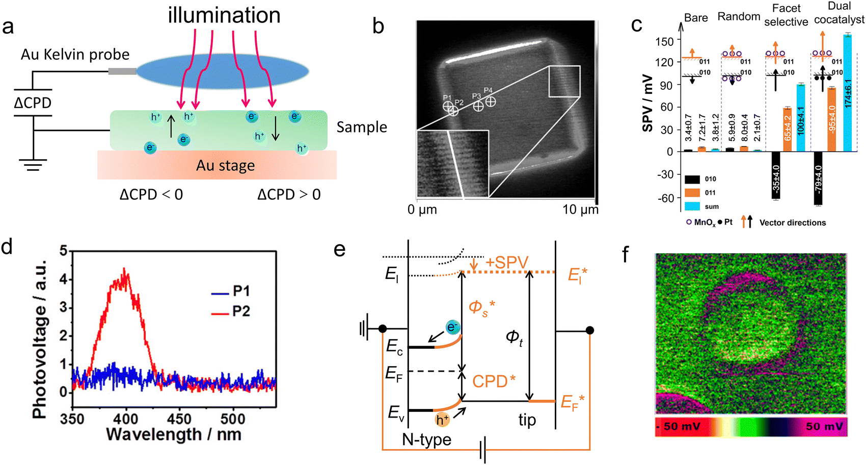 | ||
| Fig. 18 (a) Schematic diagram for the measurement of the contact potential difference in photocatalysts using KPFM technique. (b) KPFM of a single BiVO4 particle under light illumination at the wavelength of 395 nm. Reproduced with permission.218 Copyright 2015, Wiley-VCH. (c) SPV signals of {011} and {010} facets for a single BiVO4 nanoparticle with and without the decoration cocatalysts including MnOx and Pt. Reproduced with permission.219 Copyright 2017, American Chemical Society. (d) SPV spectroscopy of the TiO2 homojunction. Reproduced with permission.220 Copyright 2017, American Chemical Society. (e) Determination of the SPV by KPFM on a single photocatalyst under super-band excitation. Reproduced with permission.221 Copyright 2014, Royal Society Chemistry. (f) SPV image by subtracting the potential under dark conditions from that under 532 nm illumination. Reproduced with permission.222 Copyright 2017, American Chemical Society. | ||
Through KPFM-based SPV measurement, the holes and electrons transfer within the p–n heterojunction can also be well observed.221,223 As seen from Fig. 18e, the measured SPV can be divided into two parts, charge separation across the junction (SPVj) and the in the surface space charge region (SPVs). SPVs was positive owing to the transfer of holes to the surface, whereas the SPVj was negative and much larger than the SPVs. This implied that the p–n junction dominated the carrier transfer for efficient photocatalytic application. As a result, the measurement on the surface of the composite photocatalyst will yield a negative value, as the SPVj was greater than SPVs in most cases. Because of the short lifetime of the hot charges, inferior charge separation became the key obstacle that hindered the application of plasmon-induced chemical reaction.15,224,225 Recently, KPFM has been introduced in the nanometal–semiconductor Schottky heterojunction to provide direct information about the hot carrier accumulation location and local charge density. For typical Au/TiO2 prototype, under light illumination, the hot electrons usually migrated from the excited state of Au to the CB of TiO2, by overcoming the interfacial Schottky barrier.222 The SPV image in Fig. 18f showed the spatial distribution of hot holes in Au/TiO2, and demonstrated the holes’ accumulation in the Au/TiO2 interface. This hot charge spatial separation significantly prolonged the hot electrons’ lifetime, providing sufficient driving force for carrier transfer to the surface for chemical reactions.
In addition to the metal oxide and metal-oxide hybrid systems, the carrier transfer processes within photosensitive sulfides and carbon nitrides are accessible by KPFM. For instance, the constructed MoS2-modified CdS nanorod was reported for photocatalytic hydrogen generation, in which the effect of MoS2 on the carrier separation and overall photocatalytic performance had been thoroughly studied by KPFM.226 During the linear scanning process, no potential steps can be observed on pure CdS (whether at the tip or on the body of the nanorod). While, under the presence of tip-loaded MoS2, a significant negative surface potential of ∼16 mV emerged, which can be ascribed to the built-in electric field within the MoS2/CdS p–n junction region. The spatial separation of electrons (to the tip MoS2) and holes (to the exposed CdS surface) of CdS nanorod contributed to superior H2 production of 31.46 mmol h−1 g−1, 15 times than that of pure CdS. What's more, pure g-C3N4 (CN) always encountered sluggish carrier transfer, which lead to severe bulk recombination. To address this issue, Wu et al.227 anchored NiCo2O4 quantum dots (QDs) on the 2D C3N4 nanosheets. The surface potential changes of the composite were investigated by KPFM under both dark and light conditions. The low CPD of QDs and the high CPD of CN indicated the electric field direction from QDs to CN, and the electric field can be calculated by the surface potential differences between CN and QDs (ΔCPD). This high interfacial electric field (1.56 × 10⁴ V cm−1) induced fast carrier separation, leading to the H2 production rate of 0.36 mmol h−1 g−1 (10 times higher than that of pure CN).
Due to the high sensitivity and spatial resolution, the KPFM-based SPV measurement was a powerful tool for probing the surface potential, as well as the charge separation and distribution on individual nanocrystals or interfaces of the photocatalysts. Through the measured ΔCPD and the calculated electric field strength, the magnitude of the driving force for carrier transfer can be evaluated and quantified. However, under aqueous solution environment, it was difficult to implement KPFM because of the directional migration of free ions under AC voltage. Meanwhile, the tested samples must exhibit good conductivity and to be modified on a substrate, thus the contribution of charge transfer between sample and the substrate to the SPV signals should be further considered. Besides, KPFM technology mainly measured surface potential, which made it difficult to clearly display the distribution and dynamic process of charge carriers inside the material. Especially in complex multilayer structures or nanoscale materials, KPFM may not accurately reflect the true distribution and transport of charge carriers.
At present, the steady-state charge distribution on single photocatalyst particles has been reported which realized by microscopic techniques,228,229 and the charge transfer dynamics have been revealed by several time-resolved spectroscopy.230,231 Meanwhile, researchers have verified the transport characteristics of carriers on different crystal planes, through the indirectly approach by depositing metal nanoparticles (e.g. Pt, Au, Ag) and CoOx cocatalysts on the electron and hole-enriched facets of the single crystal, respectively.232–235 However, the direct observation of the charge separation dynamics at spatiotemporal scale in single photocatalyst particles still lacked, which hindered the in-depth understanding of the charge separation mechanism and the development of high-performance photocatalytic systems.236
Thus, for the first time, Fan and Li52 performed spatiotemporally resolved surface photovoltage (SRSPV) measurement on Cu2O single crystal photocatalyst, to monitor and map the charge transfer processes on the femtosecond to second timescale (Fig. 19). A nanosized conducting tip was utilized to measure the local SPV by extracting the changes in photo-induced surface potential, and an external lock-in amplifier was chosen to improve sensitivity. The SPV was proportional to the separated charge density and separation length, in which the signs of SPV represented the carrier transfer direction. Thus, the SRSPV signals became a robust tool to interpret the nanoscale carrier transfer process.
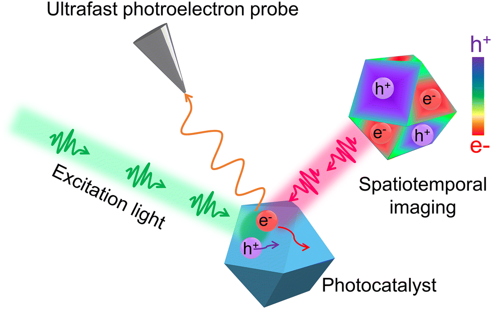 | ||
| Fig. 19 Schematic representation of proposed imaging techniques that enable spatiotemporal and operando imaging of charge-separation processes in photocatalysts. | ||
They first optimized the charge separation behavior of Cu2O particles through facet and defect engineering.237–240 The surface charge distributions on the Cu2O nanoparticles with different morphologies were mapped using SRSPV. They found that the photo-generated electrons were transferred to the catalytic surface through inter-facet hot electron transfer at the sub ps timescale, while photo-generated holes were transferred to a spatially separated surface and stabilized through selective trapping on a ms timescale. Fig. 20a quantitatively compared the SPV distributions across the {111} and {001} facets of single E-Cu2O, EH-Cu2O and H-Cu2O photocatalysts. Specifically, the photo-generated electrons tend to accumulated on the {001} facet of Cu2O nanocube (dark red region), rather than on the {111} facet of Cu2O octahedron. For truncated octahedral Cu2O, the color difference in different facets demonstrated the anisotropic charge transfer feature (electrons and holes migrate to different direction) of single Cu2O particle under illumination. With increased Cu vacancies (Vcu), the SPV of the inclined planes gradually became positive, and reached maximum for all the facets under extreme incorporation of VCu. Based on the observed anisotropic charge transfer feature, they selectively deposited Au on the {001} facet of Cu2O by photoreduction approach. SRSPV images showed that the electron transfer to the {001} facets and hole transfer to the {111} facets were enhanced after Au deposition, with the enhancement amplitude of nearly 50%. Finally, they built the relationship between the driving force of anisotropic charge transfer219 and the photocatalytic hydrogen (H2) generation performance (Fig. 20b), in which the H2 evolution rate was positively related to the anisotropic charge transfer driving force (Fig. 20c). As a result, the EH-Cu2O/Au photocatalyst exhibited a superior H2 evolution rate of ∼50 μmol h−1 g−1, about 1.56, 5, and 6.25 times higher than that of EH-Cu2O, H-Cu2O, and E-Cu2O samples. This study of spatiotemporally tracking the charge transfer process established an experimental paradigm for revealing the complex mechanisms in photocatalysis.
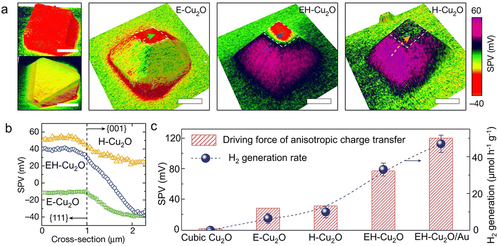 | ||
| Fig. 20 (a) SPVM images of truncated octahedral Cu2O particles without (E-Cu2O), with moderate (EH-Cu2O), and with extreme incorporation of (H-Cu2O) defects. (b) SPV distributions across the {111} and {001} facets of the three particles. (c) Driving forces of the anisotropic charge transfer and rates of photocatalytic H2 generation obtained for different Cu2O photocatalytic systems. Reproduced with permission.52 Copyright 2022, Springer Nature. | ||
In brief, spatial resolved microscopy can direct observe the carrier separation process under illumination, through monitoring the surface potential difference caused by directional migration of holes and electrons. This provided experimental evidences for some previously speculated mechanisms, to guide the optimization of the carrier separation process. Since the SRSPV technique can explore the carrier transfer on single nano crystals, it was crucial to obtain highly dispersed catalyst suspensions during sample preparation. Meanwhile, due to the extreme sensitivity of carrier transport to temperature, electric field, magnetic field, etc., real-time monitoring of laboratory environmental parameters was highly required. 4D-UEM, KPFM, and SRSPV techniques are powerful tools for in situ monitor the photo-generated carrier separation dynamics. The visualization of carrier separation process provides guidance for the scientific community to understand the carrier transport behavior more deeply, which benefits the development of high-performance semiconductor catalysts.
3.7. Density functional theory
Beyond the experimental characterizations, density functional theory (DFT) calculation method was also a powerful tool to investigate the properties of the semiconductors at the atomic/molecular level. Since the carrier transfer process was highly dependent on the electronic structure of the semiconductors, DFT method can help to analyze key information including band structure, density of states, and electron cloud distribution of semiconductor materials, which are crucial for understanding the transport mechanism of charge carriers.241,242 Early in 1927, Thomas and Fermi proposed the Thomas-Fermi model based on the assumption of a uniform electron gas in an ideal state, which firstly introduced the concept of density functional and became the prototype of DFT methods. However, this model does not consider the interaction between electrons. With continuous development of technology, DFT has undergone significant evolution and improvement. Scientists have developed methods including local density approximation (LDA), generalized gradient approximation (GGA), and Perdew–Burke–Ernzerhof (PBE), etc., continuously improving the accuracy and precision, gradually approaching the actual reaction environment. Among them, the GGA and PBE functional were widely adopted, because the former considered the gradient changes in electron density, while the later had the advantages of streamlined settings, high computational efficiency, and low cost.243,244 At present, the DFT calculations became an important tool for analyzing the electronic structure of single phase materials and interfacial electron transfer of composite photocatalysts, providing theoretical support beyond experiments for the study of carrier transport dynamics. For band gap structure, the change of VB and CB width (the more delocalized, the faster the carrier transfer), CBM and VBM position, and the emergence of mid-gap states (some of them as electron or holes’ trapping, benefiting carrier separation) can jointly influence the carrier transfer dynamics. For single phase system, intrinsic properties (mobility, diffusion length, effective mass, conductivity, etc.) which influence the carrier migration and separation can be calculated by DFT, while can hardly be obtained by experiments.30,245 For composite photocatalysts, the interfacial charge transfer, the built-in electric field intensity, and the energy band bending degree within space charge region can be quantified, to help understanding the boosted carrier transfer under illumination and identify heterojunction types, etc.246,247The differentiated performance of the photocatalysts with different exposed crystal planes were usually explained as the contribution of facet effects (for instance, surface energy, active sites, etc.). However, the differences in the carrier transport dynamics on various crystal planes had been rarely studied. In 2018, Li et al.248 successfully fabricated WO3 nanosheets and nanowires with dominant exposed facets of {001} and {110}, respectively. Through GGA calculation (Fig. 21a), the effective mass and the mobility of carriers were obtained. The lower hole effective mass on {110} (0.94m0, m0 represented the free electron mass) than on {001} (1.28m0) led to higher hole mobility of 4.92 cm2 V−1 s−1 on {110} facet, 1.56 times higher than that on {001} facet (3.14 cm2 V−1 s−1). In addition, the calculated hole diffusion length on {110} was 74.8 nm, 1.4 times larger than that on {001} (53.4 nm), which reduced the probability of bulk recombination. These results suggested that the photo-generated holes can transfer along the {110} plane of WO3 faster than that along {001}. Thus, the better hole transport behavior on {110} triggered high photocatalytic oxidation activity of WO3 nanowires, whose benzyl alcohol oxidation activity was 2.46 times as high as that of WO3 nanosheets.
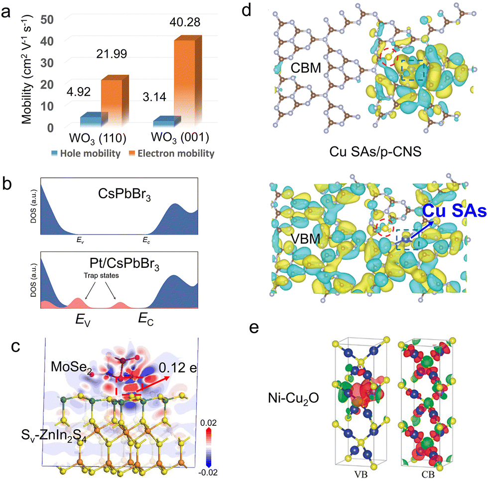 | ||
| Fig. 21 (a) Calculated hole mobility of the two WO3 samples. Reproduced with permission.248 Copyright 2018, American Chemical Society. (b) DFT calculation of the density of states (DOS) for a pure CsPbBr3 nanocrystal with a clean band gap and a Pt-SA/CsPbBr3 nanocrystal with midgap states. Reproduced with permission.249 Copyright 2021, American Chemical Society. (c) The side view of charge density difference of Sv-ZnIn2S4/MoSe2 heterostructure. Reproduced with permission.250 Copyright 2021, Springer Nature. (d) The isosurface plots of the wave function |Ψ|2 of CBM (left) and VBM (right) over the Cu SAs/p-CNS sample. The cyan and yellow areas represent electron depletion and accumulation, respectively. Red circles are the S sites and blue squares are Cu sites. Reproduced with permission.252 Copyright 2021, Wiley-VCH. (e) The difference charge density of Ni–Cu2O at VB and CB. Reproduced with permission.253 Copyright 2020, Wiley-VCH. | ||
Lead halide perovskite nanocrystals (CsPbX3 NCs) have been regarded as promising materials in photocatalysis, and the combination of metal single atoms with CsPbX3 NCs may be a practical way in exploring perovskite-based catalysts. Herein, Cao et al.249 designed a Pt single atoms-deposited CsPbBr3 NCs (Pt-SA/CsPbBr3) through a photo-assisted method, in which the Pt single atoms were anchored through the bridging of Pt–O and Pt–Br bonds on partially oxidized CsPbBr3 NCs surface. Through DFT calculation (using PBE functional), the density of state (DOS) of Pt atoms in Pt-SA/CsPbBr3 was systematically investigated. For pure CsPbBr3 NCs, no impurity levels can be observed within the band gap. While, the decoration of Pt single atoms caused the formation of trap states near the VBM and within the band gap (Fig. 21b), resulting in fast carrier separation. Thus, the optimized Pt-SA/CsPbBr3 photocatalyst exhibited high activity in photocatalytic propyne semi-hydrogenation (90.0 h−1 of turnover frequency and 86.6% of propylene selectivity).
Construction of Z-scheme heterostructure can promote the carrier separation without reducing the redox ability of holes and electrons in the composite system, to realize efficient photocatalytic application. However, the conscious modulation of the charge transfer direction was still challenging. Li et al.250 rationally fabricated Z-scheme Sv-ZnIn2S4/MoSe2 photocatalyst by a facile hydrothermal method, with abundant interfacial Mo–S bonds and internal electric field, to achieve robust photocatalytic hydrogen evolution. According to the Population analysis and Hirshfeld analysis results, the transferred charge of 0.12e between MoSe2 and Sv-ZnIn2S4 directly demonstrated the intense bond effect of Mo atom in MoSe2 and unsaturated coordinated S atom in ZnIn2S4. This bond effect was also verified by the localized distribution of the electron cloud density between Mo and S atoms (Fig. 21c). Under light irradiation, the Mo–S bond acted as an atomic level interface bridge to promote the migration of photo excited charge carriers between Sv-ZIS and MoSe2, thereby significantly accelerating Z-type charge transfer. Due to the synergistic effect of Mo–S bond, interfacial electric field, and S vacancy, the photocatalyst exhibited a high AQY of 76.48% at 420 nm. The photocatalytic hydrogen evolution rate reached 63.21 mmol g−1 h−1, which was about 18.8-fold of pristine ZIS counterpart.
The effect of element doping-induced electronic structure regulation on carrier transfer dynamics was probed by Yang et al. using DFT calculation, in which the GGA was selected for the exchange–correlation potential.251 Compared with the pristine ZnIn2S4 (ZIS), N-doped ZnIn2S4 (N-ZIS) had a slightly wider band gap, and the N element acted as the electron acceptor to induce the formation of band tail states near the VBM, causing upward shift of the VB spectrum. These states near the VBM could endow N-ZIS with metallic conductive character to inhibit the recombination of photo-excited electrons and holes. At present, the application of polymetric carbon nitride (p-CN) in photocatalysis was restricted by the low carrier separation efficiency. To address this issue, Wang and Mao252 introduced the Cu–N4 and C–S–C active sites on the surface of p-CN (Cu SAs/p-CNS), to simultaneously promote the transfer of photo-generated electrons and holes. The successful decoration of Cu–N4 and C–S–C sites on p-CN was confirmed by AC HAADF-STEM and XAS measurements. DFT calculations suggested that, during photocatalytic reaction, the isolated Cu–N4 sites and S atoms acted as electron acceptors and donors, respectively, in which the photo-induced electrons were captured by Cu sites to react with adsorbed oxygen, and the holes could react with HMF, synergistically facilitated the separation of photo-generated carriers (Fig. 21d). As a result, for the photocatalytic oxidation of 5-hydroxymethylfurfural (HMF) to 2,5-diformylfuran (DFF), the optimized Cu SAs/p-CNS catalyst exhibited a high HMF conversion efficiency of 77.1%, much higher than those of p-CN (3.7%), p-CNS (13.9%), and Cu SAs/p-CN (46.8%). While, the DFF selectivity of 85.6% was 10.9, 5.5, and 2.0 times higher than the counterparts.
Cu2O was a typical photoelectrocatalyst for sustainable hydrogen production, while the fast charge recombination hindered its further development. Hu et al.253 reported the Ni2+ doping into Cu2O lattice (Ni–Cu2O) by a simple hydrothermal method. The photocurrent density of the optimized Ni–Cu2O reached 0.83 mA cm−2, 1.34 times higher than that of pure Cu2O. The DOS was first calculated to understand the carrier transfer characteristics (using PBE functional). Relative to pure Cu2O, the introduction of Ni induced strong hybridization between Cu 3d and O 2p orbits, and the generation of impurity levels narrowed the band gap. From difference charge density results, the charges accumulation around the Ni sites in Ni–Cu2O implied the role of Ni dopants as an electron acceptor to trap electrons from Cu and O (Fig. 21e). The charge density in CB increased significantly after Ni doping, further suggesting the effective charge separation in Ni–Cu2O.
To promote the HER and OER performance separately over SrTiO3: Al photocatalysts, Domen et al.238 selectively deposited Rh/Cr2O3 and CoOOH on different facets based on anisotropic charge transport. By simulating the photocarrier distributions in SrTiO3: Al particles, the oriental transfer of electrons to Rh/Cr2O3 on {100} facets and holes to CoOOH on {110} facets are revealed. Thus, the AQE of overall water splitting reached as high as 96% between 350–360 nm region, and the activity can be maintained at 94% at least 12.5 h. In addition to overall water splitting, the integration of HER with oxidative organic synthesis is a promising way for the production of high-value chemicals. To overcome the sluggish bulk carrier transfer, Xiong et al.254 induced a full-space electric field via charge polarization engineering on a Mo cluster-decorated Zn2In2S5 (Mo-ZIS) photocatalyst. Through DFT calculations, the oriented migration of photo-electrons from [Zn–S] to [In–S] and finally to Mo sites was revealed, due to the cascade of bulk electric field and local surface electric field. Thus, the carrier lifetime extended from 0.39 (pure ZIS) to 0.76 ns, and the reduced carrier transfer resistance cooperatively demonstrated the fast carrier transfer dynamics over Mo-ZIS. Superior H2 and benzaldehyde production rates of 34.35 and 45.31 mmol gcat−1 h−1 were obtained, outperforming pristine ZIS by 3.8- and 4.1-fold, respectively.
DFT calculations can not only serve as auxiliary means to explain various phenomena in the experimental process, but also design various novel structures and predict the carrier transfer kinetics of photocatalysts under intrinsic and operating conditions, guiding the design of high-performance catalysts. In addition, theoretical calculations were not limited by sample morphology, particle size, phase, and conductivity, which were strictly required in various experimental characterization methods. Besides numerous advantages, the approximate processing of DFT calculation process was prone to introduce errors. Meanwhile, for composite photocatalysts, an excessive number of atoms may lead to time-consuming calculations and the risk of program crashes. Besides, during the process of model construction, it is strongly recommended that all researchers perform detailed characterizations to obtain the fine structure of the material (for example, the number and method of doping atoms, the coordination number of each atom, the arrangement of atoms at heterogeneous interfaces, the concentration and types of vacancies, and so on), to ensure the accuracy of the computational model. Otherwise the DFT calculation results may not in consistent with the experimental data. Therefore, when performing DFT calculations, it was necessary to comprehensively consider the factors such as actual reaction environment and the number of atoms in the material system, choosing the most suitable method and the most accurate models to avoid calculation errors.
3.8. Real-time time-dependent DFT
Traditional DFT calculations can only obtain the intrinsic electronic structure of materials in an ideal vacuum environment. As the photocatalytic process involves the generation of photo-generated charge carriers and surface chemical reactions under illumination, revealing the behavior of the photocatalysts under operating conditions can provide a more intuitive understanding of the carrier transfer characteristics. Time-dependent DFT (TDDFT) is developed based on DFT and is used to describe the behavior of electronic systems over time.255,256 It is particularly suitable for calculating excited state energy, describing electronic absorption spectra, and other properties of excited state molecules. Real-time TDDFT (rt-TDPL) is a real-time solution method for TDDFT that can simulate the dynamic characteristics of structures in excited states. By using rt-TDDFT calculation, the distribution and relaxation process of photo-generated carriers at different energy levels can be analyzed. This helps to understand carrier transfer dynamics in materials and eventually relax to the ground state.At present, rt-TDDFT was gradually utilized to accurately guide carrier separation efficiency regulation, for developing high-performance photocatalysts. Based on the rt-TDDFT, Dai et al.257 proposed that one-dimensional Janus MoSSe nanotube (A-NT) was a promising photocatalyst with high catalytic efficiency. The large electric dipole moment in A-NT induced significant interfacial built-in electric field between the inner and outer surface. To probe the effect of built-in electric field on the carrier separation, they utilized rt-TDPL to predict the timescale of the electron–hole recombination. Surprisingly, the recombination time for an electron–hole pair was up to 33 ns, two orders of magnitude longer than that of pure MoSSe monolayer and MoS2 monolayer (Fig. 22a). Ren et al.258 employed rt-TDDFT to assess carrier separation at the orbital level in ZnIn2S4 (ZIS). Series experiment measurements (PL, TRPL. Photocurrent, and PEIS) demonstrated that the N doping with the amount of 0.5% (N-ZIS) exhibited a high carrier transfer dynamics than that of pure ZIS. Then, the rt-TDDFT was used to simulate the carrier transfer under illumination (Fig. 22b). The N-ZIS suffered a stronger electron loss in VBM and accumulation in CBM, indicating enhanced electron transition between VBM and CBM, and thus the better carrier separation efficiency in N-ZIS. Besides, rt-DFT have been demonstrated as a robust tool to probe the photo-induced carrier transfer dynamics of organic semiconductors and hybrid heterojunction etc.259,260 The unique structure of 0D/2D heterojunction enabled quantum dots to be uniformly dispersed on two-dimensional nanosheets, forming tight interface contacts. Su and coworkers261 proposed a novel Au9(PH3)8/MoS2 photocatalyst as the prototype for developing robust 0D/2D heterojunction. Through rt-TDDFT calculation, they found an ultrafast electron transfer from Au9(PH3)8 to MoS2 within 20 fs, whereas the hole transferred from MoS2 to Au9(PH3)8 within 680 fs. As the electron–hole recombination required a relatively long time of 205 ns, the fast interfacial carrier transfer could enable superior photocatalytic performance.
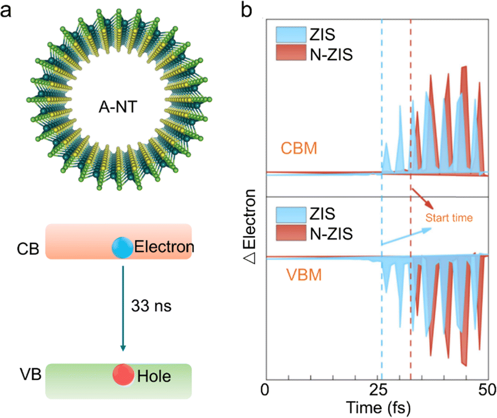 | ||
| Fig. 22 (a) Predicted atomic structure and recombination time for an electron–hole pair in MoSSe nanotube photocatalyst. Reproduced with permission.257 Copyright 2019, Royal Society Chemistry. (b) Electron occupation number of VBM and CBM under external field (to simulate photo-illumination) obtained by rt-TDDFT in ZIS and N-ZIS samples. Reproduced with permission.258 Copyright 2024, Elsevier B.V. | ||
RT-TDDFT is capable of handling time-dependent external field responses (illumination for photocatalysis), allowing it to calculate excited states and dynamic properties, which is not possible with traditional ground state DFT. Due to the real-time simulation feature, it is very useful for studying dynamic processes such as photoexcitation process, which helps to design and optimize experimental conditions. While, factors such as the influence of external fields, the size or complexity of the system, etc. can cause the calculation results to fail to converge, reducing the stability and accuracy of the results. Also, for large systems or long-term scales, significant amounts of computational resources are still required, which may limit the practicality of rt-TDDFT. In addition, non-adiabatic approximation may become a challenge when dealing with strong electronic correlations or rapidly changing external fields. This may unable to accurately describe the electron dynamics behavior in these situations. In the future research, when analyzing the carrier separation process of photocatalysts in different systems, in addition to using DFT to study the intrinsic properties of materials, rt-TDDFT technology can also be combined to further analyze the migration and transport dynamics of electrons and holes under illumination, providing valuable insights into the photocarrier dynamics.
4. Dynamic of plasmonic photo-generated carriers in catalysis
While heterogeneous photocatalysis is traditionally associated with the semiconductors (oxides, sulfides, selenides, nitrides, perovskites, etc.) – as shown in the previous sections – in recent years, the emergence of plasmonic catalysis expanded the toolbox of materials for photocatalysis to include also metallic nanostructures.38–40 Traditionally, nano-metals were deposited onto conventional semiconductors as co-catalysts to enhance carrier migration and separation. In 1996, YoKo et al.262 demonstrated that depositing Au and Ag nanoparticles onto TiO2 enabled the composite system to exhibit photoactivity under visible light. This finding revealed that nano-metals not only functioned as co-catalysts but also generated charge carriers under solar irradiation, namely plasmonic metals, overcoming the ultraviolet-only sensitivity of pure TiO2. Furthermore, charge carriers photogenerated in plasmonic metals exhibit highly energetic characteristic, enabling novel applications that leverage both their access to high energy states and the photothermal effect arising from their relaxation pathways. This breakthrough spurred extensive research into the application of nano-metals in energy and environmental photocatalysis, highlighting their potential advantages, especially in hybrid configurations. The complex role of interfaces has emerged as a pivotal factor in facilitating charge transfer, marking a significant step toward the development of advanced hybrid architectures.In plasmonic photocatalysts, localized surface plasmon resonances (LSPRs) – i.e., the collective oscillation of free electrons within the metal upon excitation with the incident radiation – enable to deposit the energy of the incoming photon into the kinetic energy of the electrons in the material.41 After LSPR excitation, plasmons decay, initially producing highly energetic charge carriers (i.e., hot carriers) that later thermalize with the phonons of the metal, leading to temperature increase.42 However, both, the plasmonic hot carriers (PHCs) and the photogenerated heat, can contribute to catalysis, either via non-thermal and/or thermal effects (Fig. 23a).42,263 Moreover, the oscillating character of the plasmon also promotes highly confined AC electric fields on the surface of the metal. Such electric field confinement can also boost chemical reactivity, constituting a third channel – besides hot-carriers and heat – to promote a catalytic reaction.15 Thus, compared with traditional semiconductors, the carrier separation in nano-metal photocatalysts highly differs, in which the same characterization may yield vastly different results, and the discussion and analysis about the carrier transfer dynamics in plasmonic photocatalysts are of great significance and importance.
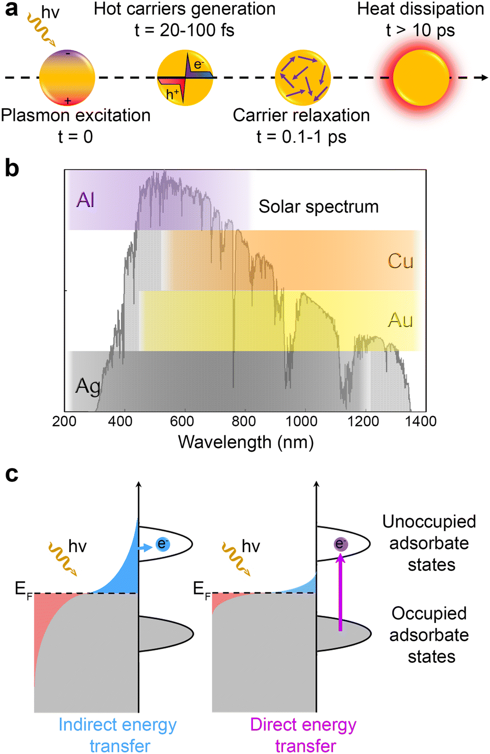 | ||
| Fig. 23 (a) Schematic of the relevant ultrafast and fast time scales of different steps involved in the internal relaxation of a collective plasmonic mode in a nanocrystal after a pulsed excitation. The initial out-of-equilibrium carrier distribution excited by the plasmon thermalizes in the scale of ∼100 fs, to then share their energy with the lattice and ultimately with its environment as heat. Reproduced with permission.42 Copyright 2020, American Chemical Society. (b) Representation of the optical region accessible through various sizes and shapes for plasmonic nano-metals (Al, Ag, Au and Cu) with the solar spectrum overlayed. (c) Schematics depicting the indirect (left) and direct (right) energy transfer mechanisms. The hot electrons are generated from plasmon relaxation, which can transfer to the metal-adsorbate states at the interface if they possess sufficient energy. Otherwise, the direct excitation of charge carriers from the adsorbate–metal states at the interface occurs during plasmon decay. Reproduced with permission.264 Copyright 2018, Springer Nature Limited. | ||
The light harvesting properties of plasmonic structures are tuned by their composition, size and shape, enabling interaction with the entire solar spectrum (Fig. 23b).265–267 Extensive reviews, focusing specifically on PHCs, delve into the associated phenomena and the remarkable ability of PHCs to drive unexpected chemical reactions.224,264,268,269 Interestingly, PHCs are generated through a surface-mediated mechanism, which localizes them at the interface of the metal and its surrounding, making them available for catalytic events.270 Such events were evidenced by microscopy techniques (e.g., SEM and TEM). It showed the evolution in morphology of the structure by following a visible chemical formation (e.g., polymerization) through sequence of images under different irradiation time.271,272 This revealed the significance of unveiling the reactivity of PHCs and the spatial location of the reactive sites related to the transfer of PHCs.
4.1. Hot-carrier transfer dynamics in plasmonic photocatalysts
By contrast to the charge carriers generated from semiconductor excitation, the PHCs are highly energetic, and consequently with smaller lifetime (tens of fs to ps, compared to the ns timescale for most semiconductors). This sets a big challenge to the mechanistic understanding in plasmonic catalysis due to the complexity of the system – many effects taking place at the same time – and the very short timescales of such processes.273 Nonetheless, intensive research efforts were performed to decipher the PHC generation, transport and utilization according to the metallic environment, e.g., adsorbates (i.e., molecules), metals and semiconductors. Critically, the previously introduced techniques to elucidate charge transfer dynamics in semiconductor apply to the mechanism of PHC transfer in metallic nanostructures. However, the localized and ultrafast properties of PHCs demanded continuous technical development of experimental setup and theoretical models to effectively answer the requirements of PHC catalysis, as evidenced by Table 6 showing a variety of carrier lifetime for PHC (from 2 fs to 2 ns for Au).274 Following, we discuss the plasmon energy transfer (PET) dynamic focusing on specific environments and their relevance for photocatalysis.| Metal | Method | Carrier lifetime | λ exc (nm) | Ref. |
|---|---|---|---|---|
| Au | TRPL | 2–20 fs | 780 | 280 |
| ≤50 fs | 410 | 281 | ||
| 0.3–3 ps | 400–6000 | 282 | ||
| ≤0.5 ps | 470 | 283 | ||
| ∼1 ps | 800 | 283 | ||
| <2.4 ps | 780 | 280 | ||
| 0.8–2 ns | 780 | 284 | ||
| TAS | 0.3 ps | 780 | 285 | |
| 3.7 ± 0.1 ps | 430 | 286 | ||
| 6.5 ps | 265 | 287 | ||
| 9 ps | 500 | 288 | ||
| Theoretical | 0.5 ps | 289 | ||
| 8 fs | 290 | |||
| Ag | TAS | 40 ± 7 fs | 610 | 291 |
| <1 ps | 400 | 292 | ||
| Theoretical | 10 fs | 293 | ||
| 1 ps | 294 | |||
| 2 ps | 294 | |||
| Cu | TR-2PP | 20–30 fs | 400 | 295 |
| TAS | 0.8–0.9 ps | 550–600 | 296 | |
| 0.7–1.3 ps | 550–570 | 296 | ||
To occur, plasmonic photocatalysis requires the plasmon energy to transfer from the metal to the adsorbed molecules. The molecules, once adsorbed, show hybridized orbitals with energies according to the metal–molecule interfacial state. The PET can take place directly and indirectly.264 The former occurs via the direct PET to the interfacial states of the metal–adsorbate (Fig. 23c). The latter takes place thanks to the generation of PHCs, which transfer from the metal to unoccupied states (i.e., orbitals) at the molecule (Fig. 23c). Boerigter et al.275 evidenced the direct transfer through significant adsorbate excitation occurring at light energy (1.6 eV) specific to the metal–adsorbate interfacial states despite a higher HOMO–LUMO energy gap of the molecule (1.86 eV). Whereas, photons of higher energy (2.33 eV) showed lower efficiency. Christopher et al. demonstrated the ability of PHCs from Ag nanostructures to oxidize molecules under visible light via kinetic isotope experiment and confirmed by DFT.276,277 A 4-fold rate enhancement was observed for the ethylene epoxidation under visible light compared to the dark conditions. They suggested that the antibonding orbitals of oxygen were populated by PHCs, which enhanced the O2 dissociation rate. Robatjazi et al. observed large photocurrents derived from the injection of plasmonic hot electrons from Au nanostructures to water molecules, driving the H2 production.278 Later, Yan et al., via time dependent DFT, suggested that the PHC energy and the unoccupied adsorbate energy level can be aligned by adjusting the nanostructure geometry and the incident light source.279 They illustrated the processes occurring under 10 fs involved during plasmon-induced water splitting at the atomic scale. These selected examples emphasize on the consequence of proper plasmonic nanostructure design to enhance the affinity with the adsorbates and the related catalytic efficiency.
4.2. Hot-carrier transfer dynamics in hybrid plasmonic photocatalysts
While plasmonic metals are recognized as great light harvesters, their catalytic efficiency is rather low in comparison with other metals (e.g., Pt, Pd, Ru). To solve this drawback, plasmonic nanostructures are combined with metals to enhance their catalytic efficiency. Typically, a plasmonic nanostructure is decorated with catalytic metals to transport the short-lived PHCs to the catalytic reactive sites, enhancing the catalytic efficiency of the overall system.297 This metal–metal structure can take different shapes (e.g., core–shell, antenna-reactor, core–satellite, metamaterial) impacting the generation of PHCs and their subsequent transfer to efficiently react at the metal–adsorbate reactive site.225 For instance, the ammonia decomposition, which usually requires high temperature and pressure, was observed on Cu–Ru antenna reactor at 27 °C under visible light excitation.298The photocatalyst efficiency was one order of magnitude higher than under dark conditions and external heating corresponding to the surface temperature measured under light excitation. The PHCs generated in the Cu plasmonic structure were identified as critical, by influencing the energetics of adsorbed nitrogen, to drive effectively the catalytic process at the Ru active sites. Using pump–probe measurements, Bykov et al. showed that, in Au–Pt heterostructure, the plasmonic hot electron transfer is enhanced by the presence of Pt.297 The relaxation of photoexcited hot–electron gas is accelerated in the presence of Pt, because of the enhancement in hot electron transfer through Au–Pt interface. They demonstrated that this effect can be controlled quantitatively by investigating various Pt concentration. Furthermore, they evidenced, thanks to electron or hole scavenger molecules, that the surrounding media influence was affecting the hot electron transfer, confirming the significance of the surrounding on the PHC transfer dynamic. Interestingly, the utilization of PHCs and electric field enhancement to localize the co-catalyst formation at the most reactive sites of the plasmonic nanostructure (i.e., hot spots) can be achieved to boost the subsequent photocatalytic activity.299,300 This metal–metal configuration is of particular interest to transfer more efficiently the PHCs to the adsorbates, despite their short lifetime, and to enhance the catalytic activity and selectivity of the photodevice, e.g., electric field enhancement.15,301
Another solution to enhance the PHC short lifetime consists in contacting the plasmonic nanostructure with a semiconductor creating a Schottky barrier, thus preventing the hot carriers to recombine after overcoming this energetic barrier. Accordingly, the lifetime of PHCs increases significantly, thus enhancing the quantum efficiency of the device (Table 7 and Fig. 24). As for the metal–adsorbate scenario, indirect and direct transfer can occur at the metal–semiconductor interface.317
| Method | Material systems | Carrier lifetime | λ exc (nm) | Ref. |
|---|---|---|---|---|
| TRPL | Ni/MCS-s | 704 ps | 300 | 302 |
| CdSe/ZnS/Au | ∼1 ns | 525 | 303 | |
| Cu–Ni/CdS | 1.79 ns | 304 | ||
| Ag/C3Nx | 7.86 ns | 325 | 173 | |
| Ag–Pt/C3Nx | 11.04 ns | 325 | 173 | |
| TAS | Au/TiO2 | 0.63 ps | 500 | 288 |
| 1.2 ps | 325 | 305 | ||
| 1.5 ns | 550 | 306 | ||
| 2.3 ns | 530 | 307 | ||
| 9.6 ns | 530 | 307 | ||
| Ag/TiO2 | 180 μs | 510 | 308 | |
| 0.5 s | 355 | 308 | ||
| Au/TiO2/W18O49 | 0.28 ps | 500 | 288 | |
| Au@CoTPyP | 3.2 ± 0.1 ps | 430 | 286 | |
| Ag–pABA–TiO2/Ru | 19 ps | 405 | 309 | |
| Ag–pABA–TiO2 | 34 ps | 405 | 309 | |
| Au/CeO2/RGO | 2.8 ± 1.4 ns | 265 | 286 | |
| Au/CeO2 | 3.5 ± 1.7 ns | 265 | 287 | |
| CuS/CdS | 9.2 μs | 1200 | 310 | |
| Au/Cu7S4 | 160 μs | 532 | 311 | |
| Au/CdS | 0.6 ± 0.1 ps | 600 | 312 | |
| 1–2 ps to 15.6 ps | 595 | 313 | ||
| 1050 ps | 650 | 314 | ||
| Au/Al2O3/Au | ∼45 fs | 1250 | 315 | |
| Au/CdSe | 1.45 ± 0.15 ps | 595 | 316 | |
| Au/CsPbBr3 | 2.6 ps | 600 | 312 | |
| Au/CdS/CsPbBr3 | 3.3 ns | 600 | 312 | |
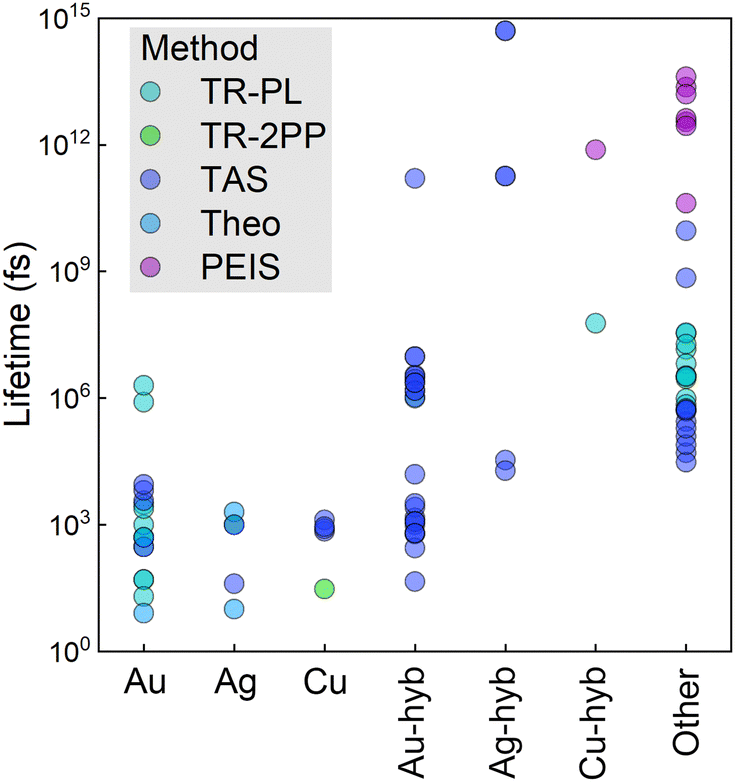 | ||
| Fig. 24 Charge carrier lifetime (fs) for plasmonic metals (Au, Ag, or Cu) and hybrid structures. (Other represents materials without plasmonic components.) Data extracted from Tables 4, 6 and 7. | ||
Understanding the PHC transfer efficiency between two interfaces is critical to enhance the charge carrier separation from the plasmonic system. Table 8 highlights different transfer efficiency according to the PHC and the metal–semiconductor interface. Roughening the semiconductor surface or embedding the metallic nanostructure in the semiconductor can enhance the charge transfer efficiency.318,319 Interestingly, the type of semiconductor (i.e., n- or p-type), which influences the band bending once contacted with the metal, enables to filter specifically the PHC of interest (i.e., hot electron or hot hole). DuChene et al. showed that the plasmonic hot holes can be transferred from Au through p-GaN.320 The separation of PHCs, thanks to the metal–semiconductor Schottky junction, enhanced the CO2 reduction at the Au NPs.
Similarly, the use of n-TiO2 enables the collection of hot electrons. For example, as detailed in Section 3.6, the photoactive sites for water oxidation at Au/TiO2 were identified at the interface of Au and TiO2 by KPFM measurements and verified by DFT calculations (Fig. 19f).222 Recently, the Au/TiO2 interfacial states were determined as critical for the charge transfer dynamic accordingly to the concentration of VOs in TiO2. As evidenced from the SPECM photoactivity (ΔI) maps, Au nanoparticles onto pristine TiO2 showed the highest ΔI at the wavelength where mostly PHCs were generated.321 However, Au nanoparticles on reduced TiO2 presented negligible ΔI to none in similar conditions. Furthermore, the ΔI from reduced TiO2 excited under blue light (455 nm) was significantly higher than the pristine one. As such, those defect sites were suggested as pathways for electrons to leak from TiO2 into the Au nanoparticles, thus quenching the plasmonic activity of the hot holes.321 Due to the sensitivity of the SPECM technique, the obtained electrochemical signal allows to identify if a thermal effect contributes to the photocatalytic reaction (Fig. 25a).322 However, uncertainties remain on the influence of plasmonic heating at the local scale, even under low power regime.323 Further, SPECM has been demonstrated as a powerful technique to locally quantify the charge transfer efficiency in hybrid nanostructures. This efficiency depends on the incident wavelength and the energy distribution of hot carriers, related to the molecules at the solid–liquid interface.324
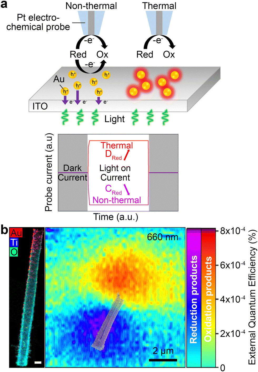 | ||
| Fig. 25 (a) Schematics of the proposed mechanisms for the photo-oxidation reaction implying (i) hot-hole generation at Au surface and (ii) thermal-induced shift in the equilibrium potential of the redox molecules. Reproduced with permission.322 Copyright 2018, American Chemical Society. (b) Left panel – Elemental mapping for the Au (red), Ti (blue) and O (green) elements of a single TiO2 nanotube decorated with Au nanoparticles similar to the nanotube studied in right panel. Right panel – External quantum efficiency map of a single nanostructure (overlayed) obtained for light excitation at 660 nm using 4.7 μW power. The scalebar in the left panel corresponds to 200 nm. Reproduced with permission.329 Copyright 2023, American Chemical Society. | ||
As such, quantum efficiency map can be obtained. At a single nanostructure, e.g., gradient of Au nanoparticles deposited on a TiO2 nanotube, a clear spatial distinction between the reduction and oxidation products was observed (Fig. 25b).329 It has been proposed that the oxidizing products were associated with the presence of hot holes at the Au–liquid interface. Simultaneously, the hot electrons ballistically diffuse into the TiO2 nanostructure to reduce molecules at the TiO2–liquid interface. Thus, the separation of hot carriers at the interface of Au/TiO2 was confirmed and spatially resolved under working conditions.329 These results were in good agreement with previous works done by TAS measurements, which evidenced the lifetime increase of the PHCs due to the charge separation at the Au/TiO2 interface (Fig. 9a).45 Through TAS measurements, Li. et al. showed the contribution of direct and indirect PET in a Ag–CuO2 core–shell nanostructure excited under visible light.330 This finding, which can be extended to other metal–semiconductor nanostructures, demonstrated the intricate contribution of both mechanisms occurring simultaneously under the light excitation. Harutyunyan et al. showed by pump–probe reflection measurements and DFT calculations that the geometry of the hot spots can control the ultrafast response of the excited metal–semiconductor interface, with the semiconductor acting as a spacer between metals.315 The intensity of this ultrafast response was directly related to the plasmonic hot electrons and the semiconductor thickness. Using semiconductor with lower Schottky barrier (e.g., TiO2 instead of Al2O3), a significant bleached component was observed, related to the injection of hot electrons into the semiconductor. Additionally, Marimuthu et al. evidenced the possibility to utilize Cu plasmonic nanostructure to switch the semiconductor shell (Cu2O) oxidation states under light excitation.331 The authors suggested that the PHCs generated at the Cu core under light excitation drive the Cu2O shell reduction to metallic Cu. They proposed that this process can take place because of the PET and the nature of the orbital interaction with the metal LSPR. PHCs can be generated in semiconductor due to the spatial confinement (e.g., 0D nanostructures like QDs).332 Indeed, the control of doping density in QDs directly influences the LSPR frequency enable its dynamic tuning. This shows the significance of spatially and temporally comprehending the dynamics of charge carriers and simultaneous energy transfer under working conditions to improve the design of future generations of photodevices.
4.3. Efficiency of hybrid plasmonic photocatalysts
The dynamics of photogenerated charge carriers directly influence the efficiency of photocatalytic devices. From photon absorption to the catalytic reaction, each step can either enhance or hinder the device photoactivity. In hybrid nanostructures, the complexity of the material multiplies with the number of interfaces. Typically, the most efficient photodevices combine a light harvesting unit (e.g., plasmonic nanostructure), a charge carrier separator (e.g., semiconductor), and a catalytic element (Fig. 26).333 The total efficiency (ηT) of the device depends on the efficiency of each step: absorption (ηA), charge carrier generation (ηeh), transfer to the reactive site (ηet and ηht), and catalytic reactivity (ηRed and ηOx). This highlights the significant role of carrier dynamics on the device efficiency (ηeh, ηet and ηht). As previously evidenced from Mubeen et al., the design of an autonomous photodevice with this type of architecture achieved an overall water splitting (solar-to-hydrogen) efficiency of ∼0.1% thanks to the hot electron filtering induced by charge separation at the metal–semiconductor interface and the presence of co-catalysts enhancing the efficiency at the photodevice–adsorbate interface.334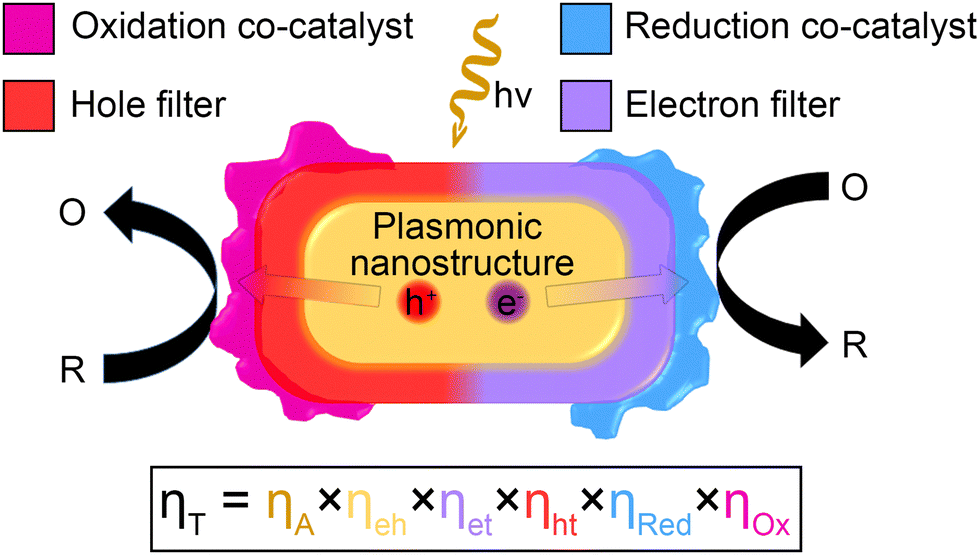 | ||
| Fig. 26 Schematic of the principal processes that contribute to the overall efficiency of a plasmonic artificial photosynthetic devicer. The total efficiency (ηT) is a contribution of the absorption efficiency (ηA), the efficiency of imparting the plasmon's energy to hot electrons and hot holes (ηeh), the efficiencies of transporting these species across boundaries to appropriate reduction and oxidation catalysts (ηet, ηht), and the efficiencies of the reduction and oxidation reactions (ηRed, ηOx). Thus, the overall efficiency can be calculated as: ηT = ηAηehηetηhtηRedηOx. Reproduced with permission.333 Copyright 2015, Springer Nature Limited. | ||
Tables 9 and 10 present recent outcomes from the literature for the photocatalytic chemical production using hybrid materials. Table 9 focuses on the H2 production, while Table 10 highlights different chemical production with hybrid photomaterials (e.g., overall water splitting (OWS), CO2 reduction, N2 reduction, etc.). These tables consider the photocatalyst performance according to the increase number of interfaces, highlighting the effect of fabrication steps on the chemical production. Fig. 27 summarizes the results from Table 9, showing the formation rate of H2 according to the EAQE for hybrid structures with and without plasmonic nanoparticles (PNPs).
| Photocatalyst | Light source | Reaction | Quantum efficiency | Formation rate (μmol g−1 h−1) | Ref. |
|---|---|---|---|---|---|
| Pt-tip-AuNR | Light source (460 < λ < 820 nm) | H2O reduction (20% CH3OH) | IQE ∼ 1% EAQE ∼ 0.68%@920 nm | ∼1950 | 338 |
| Pt-cov-AuNR | IQE ∼ 0.4% EAQE ∼ 0.27%@850 nm | ∼886 | 338 | ||
| Pt-cov-AuNS | IQE ∼ 0.15% | ∼443 | 338 | ||
| Cu–Ni/CdS | 300 W Xe lamp (≥420 nm) | H2O reduction (Na2S/Na2SO3) | EAQE 21.5%@400 nm & 12.1%@520 nm | 28190 |
304 |
| Cu/CdS | 10570 |
304 | |||
| Ni/CdS | 3510 | 304 | |||
| CdS | 320 | 304 | |||
| SiO2@CdS | LED light (λ ≥ 400 nm, 0.198 mW cm−2) | H2O reduction (Na2S/Na2SO3) | 500 | 335 | |
| Au@SiO2@CdS | 10720 |
335 | |||
| Ag@SiO2@CdS | EAQE 0.13%@470 nm | 37530 |
335 | ||
| Ag@SiO2@CdS–Au | EAQE 0.33%@470 nm | 130000 |
335 | ||
| Zn1.3Cu98.7 | Solar simulator (788 mW cm−2) | H2O reduction (CH3OH) | EAQE 6.8%@570 nm | 328000 |
339 |
| Ag–Pt/C3Nx | 300 W Xe lamp (≥420 nm) (265 mW cm−2) | H2O reduction (TEOA) | EAQE 3.3%@420 nm | 1250 | 173 |
| Pt/C3Nx | 740 | 173 | |||
| Ag/C3Nx | 35 | 173 | |||
| Ag–Au–TiO2 | 1 sun condition (100 mW cm−2) | H2O reduction (25% CH3OH) | EAQE 3.3% (370 to 650 nm) | 718 | 340 |
| Au–TiO2 | 366 | 340 | |||
| Ag–TiO2 | 355 | 340 | |||
| TiN/Pt | Monochromatic light | NH3BH3 reduction | EAQE 120%@700 nm | 341 | |
| ZnIn2S4 | Under visible light (≥420 nm) | H2O reduction (Na2S/Na2SO3) | EAQE 0.62% | 421 | 342 |
| Au/ZnIn2S4 | EAQE 2.38% | 1596 | 342 | ||
| Au@Pt/ZnIn2S4 | EAQE 6.23% | 4174 | 342 | ||
| Ag–pABA–TiO2/Ru | H2O reduction MB oxidation | QY 20% | 309 | ||
| Ag@CoFe2O4/g-C3N4 | H2O reduction (TEOA) | EAQE 16.47%@420 nm | 385600 |
343 | |
| CoFe2O4/g-C3N4 | EAQE 5.49%@420 nm | 108656 |
343 | ||
| Ag@CoFe2O4 | 2400 | 343 | |||
| Au@NiS@CNT | Xe-300 W lamp (700 nm > λ > 400 nm) | H2O reduction (TEOA) | EAQE 8.1%, EAQEMAX 15.8%@520 nm | 18500 |
344 |
| NiS@CNT | 4900 | 344 | |||
| Cu7S4 | AM 1.5 G irradiation (100 mW cm−2) | H2O reduction (5 v% CH3OH/15 wt% glucose) | EAQE 3%@400 nm | 25.1 | 311 |
| Au/Cu7S4 | EAQE 9.4%@500 nm and 7.3%@2200 nm | 211 | 311 | ||
| Au/CuSe/Pt | 300 W Xe lamp (λ > 420 nm) | H2O reduction (Na2S/Na2SO3) | EAQE 0.55%@600 nm | 4200 | 345 |
| Au/CuSe | 539 | 345 | |||
| Pt/CuSe | 431 | 345 | |||
| Au + CuSe | 117 | 345 | |||
| CuSe | 96 | 345 | |||
| Ni/MCS-s | Xe-300 W lamp (λ > 420 nm) | H2O reduction (with 3.5 wt% NaCl) | EAQE 60.4%@420 nm | 121500 (164000) |
302 |
| Pt/MCS-s | 46600 (32400) |
302 | |||
| NiS/MCS-s | (103000) |
302 | |||
| NiOH/MCS-s | (87600) |
302 | |||
| NiO/MCS-s | (82500) |
302 | |||
| MCS-s | 11800 (2400) |
302 | |||
| CdS | Visible light illumination (λ = 400–700 nm) | H2O reduction (Na2S/Na2SO3) | EAQE 2% | 314 | |
| Au/CdS | EAQE 4.8% | 314 | |||
| Au/CdS + Rh/Rh2S3 co-cat | EAQE 8.2%@320 nm – 6.2%@420 nm | 13710 |
314 | ||
| Au/g-C3N4 | Visible light (λ > 420 nm) | H2O reduction (TEOA) | EAQE 0.1%@520 nm | 540 | 346 |
| Au@CdS/Au | Visible light (λ > 400 nm) | H2O reduction (Na2S/Na2SO3) | EAQE 2.3%@450 nm | 147570 |
347 |
| Au/KCNx | Visible light (λ > 420 nm) | H2O reduction (TEOA) | EAQE 12.8%@420 nm | 8850 | 348 |
| Au/g-C3N4 | 85 | 348 | |||
| PV-PtDPA-AuNRs/CZS | Visible light (λ > 420 nm) | H2O reduction (TEOA) | EAQE 2.5%@λ > 520 nm | 587 | 349 |
| CdS & L-Cys/CdS | 300 W Xe lamp | H2O reduction (20% EtOH) | EAQE 9.14 & 14.79% | 7200 & 12390 |
350 |
| Ag/CdS | EAQE 19.18% | 16560 |
350 | ||
| Ag/L-Cys/CdS | EAQE 27.87%@450 nm 9.0 mW cm−2 | 29710 |
350 | ||
| Photocatalyst | Light source | Reaction | Products | Quantum efficiency | Formation rate (μmol g−1 h−1) | Ref. |
|---|---|---|---|---|---|---|
| a Overall water splitting. b Value obtained under bias. c Calculated on the mass of noble metal. | ||||||
| Ag@CoFe2O4/g-C3N4 | Xe-300 W lamp (λ > 420 nm–0.45 W cm−2) | OWSa | H2 and O2 | EAQE 3.35%@420 nm | 67000 and 37200 |
343 |
| Au/SrTiO3/TiO2 | AM1.5 lamp (λ > 400 nm) | OWS (KOH) | H2 and O2 | IPCE 17% EAQE 3.5% | 38 and 18 (μmol cm−2h−1)b | 351 |
| Au/CdS | LED light (640 nm–3.4 mW cm−2) | OWS | H2 and O2 | EAQE 0.24%@640 nm | ∼80 and 40 | 352 |
| C/Ag/Ag3PW12O40 | Xe-300 W lamp (λ > 420 nm) | OWS | H2 and O2 | EAQE 4.9%@480 nm | 8 and 4 | 353 |
| AgPd/g-C3N4 | Xe-300 W lamp (λ > 400 nm) | HCOOH dehydrogenation | H2 | AQE 27.8%@400 nm | 2316000 |
354 |
| Au–TiO2–Pt | Green LED light (∼550 nm) | H2O oxidation (K2Cr2O7) | O2 and Cr3+ | EAQE 1%@550 nm | 156 and 16 | 355 |
| Au/CdSe–Cu2O | 300 W Xe lamp (λ > 420 nm) | CO2 reduction (H2O with CH3CN and TEOA) | CO and CH4 | EQE 0.4%@420 nmb | 254 and 123 | 356 |
| Au–Cu2O | 31.6 and 13.5 | 356 | ||||
| CdSe–Cu2O | 41.7 and 23.2 | 356 | ||||
| Cu2O | 16.4 and 9.1 | 356 | ||||
| Ag@TiO2 | AM 1.5G 300 W lamp | CO2 reduction | CH4 | 4.93 | 357 | |
| TiO2 | 1.3 | 357 | ||||
| BiVO4–Au–Cu2O | Xe-300 W lamp (λ > 420 nm) | CO2 reduction | CH4 and CO | EAQE 0.44%@500 nm | 3.15 and 2.08 | 358 |
| Cu2O | 0.03 and 0.02 | 358 | ||||
| Ag/Ag2SO3 | 500-W Xe lamp (>400 nm) 10.75 mW cm−2 | CO2 reduction | CH4 and CO | EAQE 0.126%@∼450 nm | 3 and 1.23 | 359 |
| ZnO/Ag/CeO2 | 300 W xenon lamp | CO2 reduction (NaHCO3) | CO and CH4 | EAQE 4.47%@420 nm | 75.5 and 4.02 | 360 |
| ZnO | 1.32 and 0.07 | 360 | ||||
| CeO2 | 5.26 and 0.29 | 360 | ||||
| Au@ZIF-67 | Solar simulator (150 mW cm−2) | CO2 reduction | CH3OH and EtOH | EAQE 6.4%@420 nm | 2500 and 500 | 361 |
| Au–TiO2 | λ exc 625 & 700 nm | C6H5CH2OH oxidation | Benzaldehydes | EAQE 7.2 & 4.2% | 362 | |
| Ag superlattice/GG | LED light 100 W (400 nm–750 nm, 277 mW cm−2) | N2 reduction | NH3 | EAQE ∼0.1%@600 nm | 101c | 363 |
| Au–Ru | Xe-300 W lamp (λ > 420 nm) | N2 reduction | NH3 | 25000b |
364 | |
| Au@UiO66 | Xe-300 W lamp (>400 nm, 100 mW cm−2) | N2 reduction | NH4+ | AQE 1.54%@520 nm | 18900c |
365 |
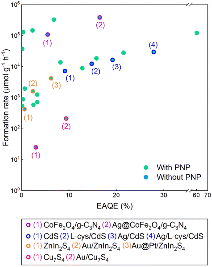 | ||
| Fig. 27 Formation rate of H2versus the external apparent quantum efficiency (selected at the wavelength corresponding to the highest efficiency) for water reduction for the different structures with and without plasmonic nanoparticles (PNPs). Each outer circle color corresponds to one reference showing the photocatalytic performance evolution through additional units composing the photodevice. | ||
The EAQE evaluates the number of electrons reacting with the molecules to successfully produce the chemical of interest (e.g., H2 here) considered as the apparent electron quantity photogenerated relative to the incident number of photons. As shown by the outer circle colour code in Fig. 27, a clear correlation appears: an increase in EAQE results in a higher formation rate. However, the varied results suggest that EAQE alone provides limited information for comparing the formation rate of H2 from different photodevices. As an example, an EAQE of 0.33% can lead to a H2 formation rate of 130 mmol g−1 h−1 on Ag@SiO2@CdS–Au while another device, Ni/Mn0.3Cd0.7Sx, with an EAQE of 60.4%, can have a very similar or even lower H2 formation rate: 121.5 mmol g−1 h−1.302,335 The EAQE encompasses all steps (ηT) at a specific photon energy in one metric, making it difficult to identify which part of the photocatalyst design needs improvement. Depending of the photon energy, the EAQE varies significantly, while the formation rate is usually recorded over a spectral window (Table 9), explaining further our observation.
Photocatalytic processes are highly dependent of the material ability to absorb photons (ηA). By considering the material as perfect absorber, the efficiency of the photogenerated carriers becomes independent of the absorption step, evaluating the carriers’ effectiveness from generation to extraction. Thus, giving a refined picture of the photocarriers fate. The IAQE displays exactly this information. By comparing EAQE and IAQE at selected wavelengths, the complexity behind an obtained formation rate becomes clearer. Yu et al.336 showed an optimal H2 formation rate of 70 mmol g−1 h−1 with InP/ZnS-S QDs under 1 sun illumination. They systematically investigated the formation rate under different light sources, and provided the EAQE and IAQE (namely AQY and IQY in ref 336) for distinct wavelengths. At 410 nm, the EAQE and IAQE were 11.2 and 24.5%, respectively. For 525 nm, a lower EAQE of 8.89% and a higher IAQE of 31% were recorded. The EAQE was 0.29% at 590 nm, while the IAQE corresponded to 12.7%, based on the obtained absorbance and EAQE.
Considering plasmonic photocatalysts, it has been shown that for gold, the IAQE is directly linked to the size of the nanoparticles, the photocatalytic reaction, the incident wavelength and the power density. Votkina et al. reported the systematic evaluation of the IAQE (namely IQE in ref. 337) according to the size of spherical Au nanoparticles (Fig. 28a). They demonstrated an evident decrease in the IAQE as the size of the nanoparticles increased, linking this to the PHCs mean free path (few nanometers).323 This was highlighted for different type of reactions (e.g., reduction, oxidation and homolysis), showing similar trend independently of the chemical reaction (related to ηRed and ηOx).
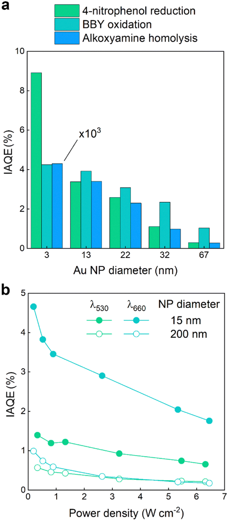 | ||
| Fig. 28 (a) Internal quantum efficiency function of the diameter of Au nanoparticles for the 4-nitrophenol reduction, Bismark brown oxidation, and alkoxyamine homolysis. The IQE values for the alkoxyamine homolysis are multiplied by 103. Reproduced with permission.337 Copyright 2024, Royal Society Chemistry. (b) Internal quantum efficiency function of the power density of the incident light according to the incident light wavelength and the diameter of the Au nanoparticles deposited on TiO2 thin film. Reproduced with permission.323 Copyright 2024, American Chemical Society. | ||
Furthermore, Henrotte et al. studied the significance of the nanoparticles size according to the photon energy and the number of photons. They reported the IAQE (namely IQE in ref. 323) decrease following the size and the number of photons (Fig. 28b). The former confirming the previous observations from Votkina et al., and the latter linking the IAQE decrease to the reaction rate limitation according to the mass transport of molecules to the reactive sites. Moreover, the type of generated carriers (PHCs versus d-holes) influenced significantly the IAQE, as evidenced by the different photon energy investigated (λexc 660 nm versus 530 nm). Noticeably, the EAQE (namely EQE in ref. 323) displayed similar values on both nanostructures, indicating the importance of focusing on distinct parameters when comparing performances.
By measuring different metrics, a refined understanding of the material intrinsic limitations can be achieved. This highlights the significance of well-defined metrics to effectively compare the photodevices and provide insightful information. Particularly when considering carrier transfer dynamics, which consists in challenging measurements, as shown in the previous sections. As such, systematic studies should be addressed to effectively compare the formation rate and the quantum efficiencies corresponding to incident and absorbed photons.
5. Summary and outlook
In this review, we conclude the significance of carrier transfer dynamics investigation in photocatalysis, and summarize the direct and indirect characterization approaches. Although numerous efforts have been devoted, there are still much challenges for the future development in this field. Therefore, we briefly discuss the research prospects and challenges below:(1) Targeted control of the properties of holes or electrons based on the intrinsic characteristics of semiconductors. At present, the improved catalytic activities by various strategies are generally attributed to the rapid electron and hole separation. However, the intrinsic properties of holes and electrons vary in different types of semiconductors. In general, compared with free electrons with fast transmission rate, the holes in VB exhibit lower mobility due to the strong binding force from atomic nuclei. Under this condition, further improving the electron transfer rate does not significantly improve the separation efficiency of charge carriers, but should be targeted to regulate the nature of the hole.
(2) Determine the types of impurity energy levels introduced by various defects. Introducing impurity states can induce trapping centers within the band gap of semiconductors. Whether the trapping effect is beneficial for secondary excitation or leads to severe recombination requires further in-depth research using the specific characterization approaches. In n-type semiconductors, non-metallic vacancies with low content can benefits the secondary excitation through trapping electrons. However, excessive amount could lead to obvious mid-gap states appears near the intrinsic Fermi level, acting as the carrier recombination center to deteriorate the performance. Thus, accurately locating the position of impurity energy levels with advanced characterization methods is essential, but there are still technical bottlenecks that require further in-depth research.
(3) Reducing interferences in the characterization process and improve accuracy. For instance, PEIS measurements require that the photoactive materials anchored on conductive FTO or ITO glass. However, the loading method of semiconductors has significant impacts on the test results, especially through non in situ methods. Due to the artificial errors, poor electrode uniformity can lead to misjudgment of carrier transport dynamics. For SCLC measurement, all the layers in the device should be smooth to avoid the interfacial defects and short circuit. However, the fabrication methods of different layers vary, which lead to inevitable poor contact between each layer. This may affect the accuracy of the calculated carrier mobility. Therefore, it is necessary to first optimize the film quality of photocatalysts on the surface of conductive substrates under different solvent systems. Meanwhile, during the testing process, multiple repeated tests should be conducted on different areas and the average value was taken to eliminate errors caused by insufficient dispersion and artificial error.
(4) Collaborative characterizations to deeply unveil the carrier transfer dynamics. In the future research of photocatalysis, the commonly utilized PL, TRPL, and PEIS techniques etc. cannot fully satisfy the in-depth exploration and the mechanism analyzation. The collaborative characterization using multiple quantitative and visual experiments is becoming increasingly necessary. Also, DFT calculations can provide the information beyond experiments, such as charge distribution, accumulation regions and energy levels of electrons and holes.
(5) Providing clear experimental details is needed to benchmark the various photodevices according to distinct metrics. This requires great efforts from the whole community to systematically make available all information related to the investigated photosystem. Moreover, harmonizing the metrics along the solar-to-energy field is a key task to clarify the appraisal of photodevices. For example, AQY and AQE are inconsistent metrics typically utilized. To do so, we summarize all the key metrics in Table 11. We include also the type of information reported and the techniques that can be used to evaluate and measure them. We expect that this table help in guiding future works in photocatalysis.
| Metric | Description | Possible methods |
|---|---|---|
| Carrier lifetime (τ) | Average time photogenerated electron or hole exist before recombination | TRPL, TAS, TRIR, transient photocurrent/photovoltage |
| Carrier mobility (μ) | Ability of charge carriers to move along a material | TOF, SCLC |
| Carrier diffusion length (L) | Average distance carriers travel before recombination | Optical pump–probe, TRPL with spatial resolution, 4D-UEM |
| Recombination rate (k) | Rate at which photogenerated carriers recombine | TRPL, TAS, IMPS |
| Charge separation efficiency (CSE) | Efficiency with which photogenerated electrons and holes are separated and utilized in photoreactions | PEIS, IMPS, SPECM, spatiotemporally resolved surface photovoltage method |
| Density of states (DOS) | Energy levels within the bandgap where charge carriers can be trapped | KPFM, DFT |
| EQE | Ratio of charge carriers collected to incident photons | PEIS, IMPS, SPECM |
| IQE | Ratio of charge carriers collected to absorbed photons | Similar to EQE combined with optical measurements (e.g., DRS) |
| EAQE | Ratio of charge carriers participating in the photocatalytic reaction to incident photons | PEIS, IMPS, SPECM |
| IAQE | Ratio of the number of charge carriers participating in the photocatalytic reaction to absorbed photons | Similar to EAQE combined with optical measurements (e.g., DRS) |
| EQY | Ratio of photocatalytic products formed to incident photons | SPECM, GC, MS, TRIR |
| IQY | Ratio of photocatalytic products formed to absorbed photons | Similar to EQY combined with optical measurements (e.g., DRS) |
(6) Reduce the errors in the DFT calculation process and comprehensively consider the actual reaction conditions as much as possible, making DFT a powerful tool for analyzing the carrier transport process in photocatalysts. At present, the DFT calculation are mostly operated in vacuum condition, and the property of the materials differ from that under photocatalytic reaction. For solid–liquid reaction system, solvent effect should be taken into account to simulate the actual environment. Meanwhile, the precise atomic and electronic structure of the photocatalysts (whether single phase or composite) should be analysed in detail, to ensure the accuracy of the constructed model. In future exploration, the development of multi-scale simulation methods can help to improve the accuracy for actual photocatalytic reaction environment, to screen out the photocatalytic materials with fast carrier transport characteristics. While, how to balance computational accuracy, cost, and efficiency is a key concern for researchers and also the program developers.
(7) For plasmonic catalysts, technical limitations impede the effective correlation between pulsed and continuous wave excitation, a challenge we deem critical to surmount. Further, the complexity of recent photodevices increases drastically with multi-layers of materials. Thus, an in-depth understanding of interfacial states and the related charge transfer dynamic of plasmonic carriers becomes necessary to effectively enhance their quantum efficiency for photocatalysis.
All in all, characterizing the dynamics of carrier transfer at both the temporal and spatial scales can provide theoretical guidance for the development of new and efficient photocatalysts. This will undoubtedly assist the green transformation of solar energy into chemical energy, aligning with the principles of sustainable development.
Data availability
No primary research results, software or code have been included and no new data were generated or analysed as part of this review.Conflicts of interest
There are no conflicts to declare.Acknowledgements
We gratefully thank the Foundation for Innovative Research Groups of the National Natural Science Foundation of China (No. 52121004), the National Natural Science Foundation of China (Grant No. 22002189, 22376222, 52372253 and 52202125), the National Key Research and Development Program of China (Grant No. 2024YFC3712104), Science and Technology Innovation Program of Hunan Province (Grant No. 2023RC1012), Central South University Research Programme of Advanced Interdisciplinary Studies (Grant No. 2023QYJC012), and Central South University Innovation-Driven Research Programme (Grant No. 2023CXQD042). We acknowledge funding and support from the Deutsche Forschungsgemeinschaft (DFG, German Research Foundation) under Germany's Excellence Strategy – EXC 2089/1 – 390776260, the Bavarian program Solar Technologies Go Hybrid (SolTech), the Center for NanoScience (CeNS) and the European Commission through the ERC SURFLIGHT. We acknowledge the support of the Czech Science Foundation (GACR) through the award no. 22-26416S.Notes and references
- J. Fu, K. Jiang, X. Qiu, J. Yu and M. Liu, Mater. Today, 2020, 32, 222–243 CrossRef CAS.
- J. Lv, J. Xie, A. G. A. Mohamed, X. Zhang and Y. Wang, Chem. Soc. Rev., 2022, 51, 1511–1528 RSC.
- X.-Q. Wang, Q. Chen, Y.-J. Zhou, H.-M. Li, J.-W. Fu and M. Liu, Adv. Sens. Energy Mater., 2022, 1, 100023 CrossRef.
- J. Wang, L. Jiang, F. Liu, M. Jia, M. Liu, J. Li and Y. Lai, Chem. Eng. J., 2021, 407, 127195 CrossRef CAS.
- W. Yang, R. R. Prabhakar, J. Tan, S. D. Tilley and J. Moon, Chem. Soc. Rev., 2019, 48, 4979–5015 RSC.
- S. Wang, G. Liu and L. Wang, Chem. Rev., 2019, 119, 5192–5247 CrossRef CAS PubMed.
- P. M. Ismail, S. Ali, S. Ali, J. Li, M. Liu, D. Yan, F. Raziq, F. Wahid, G. Li, S. Yuan, X. Wu, J. Yi, J. S. Chen, Q. Wang, L. Zhong, Y. Yang, P. Xia and L. Qiao, Adv. Mater., 2023, 35, 2303047 CrossRef CAS PubMed.
- A. Fujishima and K. Honda, Nature, 1972, 238, 37–38 CrossRef CAS PubMed.
- L. Zhang, J. Zhang, H. Yu and J. Yu, Adv. Mater., 2022, 34, 2107668 CrossRef CAS PubMed.
- J. Wang, S. Liu, T. Liu, J. Wang, F. Liu, M. Jia, J. Li, Y. Lai, Y. Zhao, L. Jiang, Y. Li and T. Zhai, Adv. Funct. Mater., 2023, 33, 2302809 Search PubMed.
- K. Yan, P. Karthick Kannan, D. Doonyapisut, K. Wu, C. H. Chung and J. Zhang, Adv. Funct. Mater., 2020, 31, 2008227 CrossRef.
- Z. Li and M. Zhu, Chem. Commun., 2020, 56, 14541–14552 RSC.
- J. Fu, S. Wang, Z. Wang, K. Liu, H. Li, H. Liu, J. Hu, X. Xu, H. Li and M. Liu, Front. Phys., 2020, 15, 33201 Search PubMed.
- X. Wang, Q. Chen, Y. Zhou, Y. Tan, Y. Wang, H. Li, Y. Chen, M. Sayed, R. A. Geioushy, N. K. Allam, J. Fu, Y. Sun and M. Liu, Nano Res., 2024, 17, 1101–1106 CrossRef CAS.
- M. Herran, S. Juergensen, M. Kessens, D. Hoeing, A. Köppen, A. Sousa-Castillo, W. J. Parak, H. Lange, S. Reich, F. Schulz and E. Cortés, Nat. Catal., 2023, 6, 1205–1214 CrossRef CAS.
- R. Shah, S. Ali, F. Raziq, S. Ali, P. M. Ismail, S. Shah, R. Iqbal, X. Wu, W. He, X. Zu, A. Zada, Adnan, F. Mabood, A. Vinu, S. H. Jhung, J. Yi and L. Qiao, Coord. Chem. Rev., 2023, 477, 214968 CrossRef CAS.
- X. Sheng, T. Xu and X. Feng, Adv. Mater., 2019, 31, 1805132 CrossRef PubMed.
- Y. Wang, W. Tian, C. Chen, W. Xu and L. Li, Adv. Funct. Mater., 2019, 29, 1809036 CrossRef.
- J. Fu, K. Liu, K. Jiang, H. Li, P. An, W. Li, N. Zhang, H. Li, X. Xu, H. Zhou, D. Tang, X. Wang, X. Qiu and M. Liu, Adv. Sci., 2019, 6, 1900796 CrossRef CAS PubMed.
- J.-B. Pan, B.-H. Wang, S. Shen, L. Chen and S.-F. Yin, Angew. Chem., Int. Ed., 2023, 62, e202307246 CrossRef CAS PubMed.
- Z. Wu, X. Liu, H. Li, Z. Sun, M. Cao, Z. Li, C. Fang, J. Zhou, C. Cao, J. Dong, S. Zhao and Z. Chen, Nat. Commun., 2023, 14, 2574 CrossRef CAS PubMed.
- J. Low, J. Yu, M. Jaroniec, S. Wageh and A. A. Al-Ghamdi, Adv. Mater., 2017, 29, 1601694 CrossRef PubMed.
- J. H. Kim and J. S. Lee, Adv. Mater., 2019, 31, e1806938 CrossRef PubMed.
- S. Li, W. Xu, L. Meng, W. Tian and L. Li, Small Sci., 2022, 2, 2100112 CrossRef CAS PubMed.
- Z. Wang and L. Wang, Chin. J. Catal., 2018, 39, 369–378 CrossRef CAS.
- R. Yanagi, T. Zhao, D. Solanki, Z. Pan and S. Hu, ACS Energy Lett., 2022, 7, 432–452 CrossRef CAS.
- S. Ali, G. Yasin, R. Iqbal, X. Huang, J. Su, S. Ibraheem, Z. Zhang, X. Wu, F. Wahid, P. M. Ismail, L. Qiao and H. Xu, Mol. Catal., 2022, 524, 112285 CrossRef CAS.
- A. Hagen, M. Steiner, M. B. Raschke, C. Lienau, T. Hertel, H. Qian, A. J. Meixner and A. Hartschuh, Phys. Rev. Lett., 2005, 95, 197401 CrossRef PubMed.
- O. P. Dimitriev, Chem. Rev., 2022, 122, 8487–8593 CrossRef CAS PubMed.
- J. Xue, M. Fujitsuka, T. Tachikawa, J. Bao and T. Majima, J. Am. Chem. Soc., 2024, 146, 8787–8799 CrossRef CAS PubMed.
- S. Corby, R. R. Rao, L. Steier and J. R. Durrant, Nat. Rev. Mater., 2021, 6, 1136–1155 CrossRef CAS.
- L. Qiao, W.-H. Fang, R. Long and O. V. Prezhdo, Angew. Chem., Int. Ed., 2020, 59, 4684–4690 CrossRef CAS PubMed.
- R. Chen, F. Fan, T. Dittrich and C. Li, Chem. Soc. Rev., 2018, 47, 8238–8262 RSC.
- M. Ebihara, T. Ikeda, S. Okunaka, H. Tokudome, K. Domen and K. Katayama, Nat. Commun., 2021, 12, 3716 CrossRef CAS PubMed.
- R. Marschall, Adv. Funct. Mater., 2014, 24, 2421–2440 CrossRef CAS.
- F. Chen, T. Ma, T. Zhang, Y. Zhang and H. Huang, Adv. Mater., 2021, 33, 2005256 CrossRef CAS PubMed.
- M. Xia, X. Zhao, Y. Zhang, W. Pan and D. Y. C. Leung, J. Mater. Chem. A, 2022, 10, 25380–25405 RSC.
- P. Christopher, H. Xin and S. Linic, Nat. Chem., 2011, 3, 467–472 CrossRef CAS PubMed.
- E. Cortés, R. Grzeschik, S. A. Maier and S. Schlücker, Nat. Rev. Chem., 2022, 6, 259–274 CrossRef PubMed.
- S. Li, P. Miao, Y. Zhang, J. Wu, B. Zhang, Y. Du, X. Han, J. Sun and P. Xu, Adv. Mater., 2021, 33, 2000086 CrossRef CAS PubMed.
- J. B. Khurgin, Nat. Nanotechnol., 2015, 10, 2–6 CrossRef CAS PubMed.
- E. Cortés, L. V. Besteiro, A. Alabastri, A. Baldi, G. Tagliabue, A. Demetriadou and P. Narang, ACS Nano, 2020, 14, 16202–16219 CrossRef PubMed.
- H. Yang, Y. Liu, Y. Ding, F. Li, L. Wang, B. Cai, F. Zhang, T. Liu, G. Boschloo, E. M. J. Johansson and L. Sun, Nat. Commun., 2023, 14, 5486 CrossRef CAS PubMed.
- T. Liu, W. Li, D. Z. Wang, T. Luo, M. Fei, D. Shin, M. M. Waegele and D. Wang, Angew. Chem., Int. Ed., 2023, 62, e202307909 CrossRef CAS PubMed.
- X. Dai, Z. Jiao, Z. Ma, K. Liu, C. Wang and H. Su, J. Phys. Chem. C, 2019, 123, 20325–20332 CrossRef CAS.
- J. Estrada-Pomares, S. Ramos-Terrón, G. Lasarte-Aragonés, R. Lucena, S. Cárdenas, D. Rodríguez-Padrón, R. Luque and G. de Miguel, J. Mater. Chem. A, 2022, 10, 11298–11305 RSC.
- F. Raziq, K. Khan, S. Ali, S. Ali, H. Xu, I. Ali, A. Zada, P. Muhammad Ismail, A. Ali, H. Khan, X. Wu, Q. Kong, M. Zahoor, H. Xiao, X. Zu, S. Li and L. Qiao, Chem. Eng. J., 2022, 446, 137161 CrossRef CAS.
- G. Žerjav, J. Zavašnik, J. Kovač and A. Pintar, Appl. Surf. Sci., 2021, 543, 148799 CrossRef.
- W. Liao, W. Chen, S. Lu, S. Zhu, Y. Xia, L. Qi, M.-Q. Yang and S. Liang, ACS Appl. Mater. Interfaces, 2021, 13, 38239–38247 CrossRef CAS PubMed.
- J. Zhang, B. Zhu, L. Zhang and J. Yu, Chem. Commun., 2023, 59, 688–699 RSC.
- A. Dey, F. A. Rahimi, S. Barman, A. Hazra and T. K. Maji, J. Mater. Chem. A, 2023, 11, 13615–13622 RSC.
- R. Chen, Z. Ren, Y. Liang, G. Zhang, T. Dittrich, R. Liu, Y. Liu, Y. Zhao, S. Pang, H. An, C. Ni, P. Zhou, K. Han, F. Fan and C. Li, Nature, 2022, 610, 296–301 CrossRef CAS PubMed.
- L. Pan, Y. Liu, L. Yao, R. Dan, K. Sivula, M. Grätzel and A. Hagfeldt, Nat. Commun., 2020, 11, 318 CrossRef CAS PubMed.
- Y. Wy, H. Jung, J. W. Hong and S. W. Han, Acc. Chem. Res., 2022, 55, 831–843 CrossRef CAS PubMed.
- J. Li, Z. Lou and B. Li, J. Mater. Chem. A, 2021, 9, 18818–18835 RSC.
- M. Xiao, B. Luo, S. Wang and L. Wang, J. Energy Chem., 2018, 27, 1111–1123 CrossRef.
- A. Kudo and Y. Miseki, Chem. Soc. Rev., 2009, 38, 253–278 RSC.
- Q. Guo, C. Zhou, Z. Ma and X. Yang, Adv. Mater., 2019, 31, 1901997 CrossRef CAS PubMed.
- R. Woods-Robinson, Y. Han, H. Zhang, T. Ablekim, I. Khan, K. A. Persson and A. Zakutayev, Chem. Rev., 2020, 120, 4007–4055 CrossRef CAS PubMed.
- W. Yu, J. Zhang and T. Peng, Appl. Catal., B, 2016, 181, 220–227 CrossRef CAS.
- P. Lianos, Appl. Catal., B, 2017, 210, 235–254 CrossRef CAS.
- G. Ou, Y. Xu, B. Wen, R. Lin, B. Ge, Y. Tang, Y. Liang, C. Yang, K. Huang, D. Zu, R. Yu, W. Chen, J. Li, H. Wu, L.-M. Liu and Y. Li, Nat. Commun., 2018, 9, 1302 CrossRef PubMed.
- M. Zhang, J. Wang, H. Xue, J. Zhang, S. Peng, X. Han, Y. Deng and W. Hu, Angew. Chem., Int. Ed., 2020, 59, 18463–18467 CrossRef CAS PubMed.
- A. Ghobadi, T. G. Ulusoy Ghobadi, F. Karadas and E. Ozbay, Adv. Opt. Mater., 2019, 7, 1900028 CrossRef.
- L. Tian, Q. Xin, C. Zhao, G. Xie, M. Z. Akram, W. Wang, R. Ma, X. Jia, B. Guo and J. R. Gong, Small, 2021, 17, 2006530 CrossRef CAS PubMed.
- M. Sayed, J. Yu, G. Liu and M. Jaroniec, Chem. Rev., 2022, 122, 10484–10537 CrossRef CAS PubMed.
- S. Ezendam, M. Herran, L. Nan, C. Gruber, Y. Kang, F. Gröbmeyer, R. Lin, J. Gargiulo, A. Sousa-Castillo and E. Cortés, ACS Energy Lett., 2022, 7, 778–815 CrossRef CAS PubMed.
- M. Fang, X. Tan, Z. Liu, B. Hu and X. Wang, Research, 2021 Search PubMed.
- J. Fu, Q. Xu, J. Low, C. Jiang and J. Yu, Appl. Catal., B, 2019, 243, 556–565 CrossRef CAS.
- C. Wang, C. You, K. Rong, C. Shen, F. Yang and S. Li, Acta Phys. -Chim. Sin., 2024, 40, 2307045 CrossRef.
- L. Xiao, W. Ren, S. Shen, M. Chen, R. Liao, Y. Zhou and X. Li, Acta Phys. -Chim. Sin., 2024, 40, 2308036 CrossRef.
- X. Li, C. Garlisi, Q. Guan, S. Anwer, K. Al-Ali, G. Palmisano and L. Zheng, Mater. Today, 2021, 47, 75–107 CrossRef CAS.
- J. Abdul Nasir, A. Munir, N. Ahmad, T. U. Haq, Z. Khan and Z. Rehman, Adv. Mater., 2021, 33, 2105195 CrossRef CAS PubMed.
- Y. Xiao, C. Feng, J. Fu, F. Wang, C. Li, V. F. Kunzelmann, C.-M. Jiang, M. Nakabayashi, N. Shibata, I. D. Sharp, K. Domen and Y. Li, Nat. Catal., 2020, 3, 932–940 CrossRef CAS.
- J. Wang, G. Ni, W. Liao, K. Liu, J. Chen, F. Liu, Z. Zhang, M. Jia, J. Li, J. Fu, E. Pensa, L. Jiang, Z. Bian, E. Cortes and M. Liu, Angew. Chem., Int. Ed., 2023, 62, e202217026 CrossRef CAS PubMed.
- D. Xiang, Z. Liu, M. Wu, H. Liu, X. Zhang, Z. Wang, Z. L. Wang and L. Li, Small, 2020, 16, 1907603 CrossRef CAS PubMed.
- W. Lei, Y. Yu, H. Zhang, Q. Jia and S. Zhang, Mater. Today, 2022, 52, 133–160 CrossRef CAS.
- D. Jiang, Z. Liu, L. Fu and H. Yang, ACS Appl. Mater. Interfaces, 2020, 12, 9872–9880 CrossRef CAS PubMed.
- T. Han, X. Cao, K. Sun, Q. Peng, C. Ye, A. Huang, W.-C. Cheong, Z. Chen, R. Lin, D. Zhao, X. Tan, Z. Zhuang, C. Chen, D. Wang and Y. Li, Nat. Commun., 2021, 12, 4952 CrossRef CAS PubMed.
- G. Chen, H. Li, Y. Zhou, C. Cai, K. Liu, J. Hu, H. Li, J. Fu and M. Liu, Nanoscale, 2021, 13, 13604–13609 RSC.
- S. Torabi, F. Jahani, I. Van Severen, C. Kanimozhi, S. Patil, R. W. A. Havenith, R. C. Chiechi, L. Lutsen, D. J. M. Vanderzande, T. J. Cleij, J. C. Hummelen and L. J. A. Koster, Adv. Funct. Mater., 2015, 25, 150–157 CrossRef CAS.
- M. B. Price, P. A. Hume, A. Ilina, I. Wagner, R. R. Tamming, K. E. Thorn, W. Jiao, A. Goldingay, P. J. Conaghan, G. Lakhwani, N. J. L. K. Davis, Y. Wang, P. Xue, H. Lu, K. Chen, X. Zhan and J. M. Hodgkiss, Nat. Commun., 2022, 13, 2827 CrossRef CAS PubMed.
- L. Wang, Y. Kong, Y. Fang, P. Cai, W. Lin and X. Wang, Adv. Funct. Mater., 2022, 32, 2208101 CrossRef CAS.
- S. Wang, Z. Ai, X. Niu, W. Yang, R. Kang, Z. Lin, A. Waseem, L. Jiao and H.-L. Jiang, Adv. Mater., 2023, 35, 2302512 CrossRef CAS PubMed.
- Z.-A. Lan, G. Zhang, X. Chen, Y. Zhang, K. A. I. Zhang and X. Wang, Angew. Chem., Int. Ed., 2019, 58, 10236–10240 CrossRef CAS PubMed.
- B. Xiao, T. Lv, J. Zhao, Q. Rong, H. Zhang, H. Wei, J. He, J. Zhang, Y. Zhang, Y. Peng and Q. Liu, ACS Catal., 2021, 11, 13255–13265 CrossRef CAS.
- W. Zhou and H. Fu, Inorg. Chem. Front., 2018, 5, 1240–1254 RSC.
- Y. Xu, H. Li, B. Sun, P. Qiao, L. Ren, G. Tian, B. Jiang, K. Pan and W. Zhou, Chem. Eng. J., 2020, 379, 122295 CrossRef CAS.
- Z. Wang, Y. Luo, T. Hisatomi, J. J. M. Vequizo, S. Suzuki, S. Chen, M. Nakabayashi, L. Lin, Z. Pan, N. Kariya, A. Yamakata, N. Shibata, T. Takata, K. Teshima and K. Domen, Nat. Commun., 2021, 12, 1005 CrossRef CAS PubMed.
- J. Xiong, J. Di, J. Xia, W. Zhu and H. Li, Adv. Funct. Mater., 2018, 28, 1801983 CrossRef.
- X. Zhang, P. Zhai, Y. Zhang, Y. Wu, C. Wang, L. Ran, J. Gao, Z. Li, B. Zhang, Z. Fan, L. Sun and J. Hou, J. Am. Chem. Soc., 2021, 143, 20657–20669 CrossRef CAS PubMed.
- R. T. Gao, J. Zhang, T. Nakajima, J. He, X. Liu, X. Zhang, L. Wang and L. Wu, Nat. Commun., 2023, 14, 2640 CrossRef CAS PubMed.
- C. Ding, J. Shi, Z. Wang and C. Li, ACS Catal., 2016, 7, 675–688 CrossRef.
- F. Li, L. Cheng, J. Fan and Q. Xiang, J. Mater. Chem. A, 2021, 9, 23765–23782 RSC.
- T. Kirchartz, J. A. Márquez, M. Stolterfoht and T. Unold, Adv. Energy Mater., 2020, 10, 1904134 CrossRef CAS.
- T. Tachikawa and T. Majima, Chem. Soc. Rev., 2010, 39, 4802–4819 RSC.
- X. Ning and G. Lu, Nanoscale, 2020, 12, 1213–1223 RSC.
- J. Fu, Z. Fan, M. Nakabayashi, H. Ju, N. Pastukhova, Y. Xiao, C. Feng, N. Shibata, K. Domen and Y. Li, Nat. Commun., 2022, 13, 729 CrossRef CAS PubMed.
- Q. Xu, B. Zhu, B. Cheng, J. Yu, M. Zhou and W. Ho, Appl. Catal., B, 2019, 255, 117770 CrossRef CAS.
- A. A. B. Baloch, F. H. Alharbi, G. Grancini, M. I. Hossain, M. K. Nazeeruddin and N. Tabet, J. Phys. Chem. C, 2018, 122, 26805–26815 CrossRef CAS.
- G. Wang, Z. Chen, T. Wang, D. Wang and J. Mao, Angew. Chem., Int. Ed., 2022, 61, e202210789 CrossRef CAS PubMed.
- X. Yan, M. Xia, H. Liu, B. Zhang, C. Chang, L. Wang and G. Yang, Nat. Commun., 2023, 14, 1741 CrossRef CAS PubMed.
- Y.-C. Chang, S.-Y. Shiau and M. Combescot, Phys. Rev. B, 2018, 98, 235203 CrossRef CAS.
- E. V. Shornikova, D. R. Yakovlev, N. A. Gippius, G. Qiang, B. Dubertret, A. H. Khan, A. Di Giacomo, I. Moreels and M. Bayer, Nano Lett., 2021, 21, 10525–10531 CrossRef CAS PubMed.
- W. Zhang, Z. Deng, J. Deng, C.-T. Au, Y. Liao, H. Yang and Q. Liu, J. Mater. Chem. A, 2022, 10, 22419–22427 RSC.
- H. Wang, S. Jin, X. Zhang and Y. Xie, Angew. Chem., Int. Ed., 2020, 59, 22828–22839 CrossRef CAS PubMed.
- X. Chi, Z.-A. Lan, Q. Chen, X. Zhang, X. Chen, G. Zhang and X. Wang, Angew. Chem., Int. Ed., 2023, 62, e202303785 CrossRef CAS PubMed.
- H. Yin, J. Chen, P. Guan, D. Zheng, Q. Kong, S. Yang, P. Zhou, B. Yang, T. Pullerits and K. Han, Angew. Chem., Int. Ed., 2021, 60, 22693–22699 CrossRef CAS PubMed.
- S. Karmakar, S. Biswas and P. Kumbhakar, Appl. Surf. Sci., 2018, 455, 379–391 CrossRef CAS.
- J. Zhou, J. Zhang, J. Zhao, H. Wang and R. Liu, J. Mater. Chem. A, 2021, 9, 16522–16531 RSC.
- J. Zhang, L. Wang, C. Jiang, B. Cheng, T. Chen and J. Yu, Adv. Sci., 2021, 8, 2102648 CrossRef CAS PubMed.
- T. Goswami, H. Bhatt, D. K. Yadav and H. N. Ghosh, Phys. Chem. Chem. Phys., 2022, 24, 19121–19143 RSC.
- J. Ma, T. J. Miao and J. Tang, Chem. Soc. Rev., 2022, 51, 5777–5794 RSC.
- T. J. Miao and J. Tang, J. Chem. Phys., 2020, 152, 194201 CrossRef CAS PubMed.
- Z. Yan, W. Wang, L. Du, J. Zhu, D. L. Phillips and J. Xu, Appl. Catal., B, 2020, 275, 119151 CrossRef CAS.
- L. Wang, W. Lian, B. Liu, H. Lv, Y. Zhang, X. Wu, T. Wang, J. Gong, T. Chen and H. Xu, Adv. Mater., 2022, 34, 2200723 CrossRef CAS PubMed.
- J. A. Christians and P. V. Kamat, ACS Nano, 2013, 7, 7967–7974 CrossRef CAS PubMed.
- R. Tang, X. Wang, W. Lian, J. Huang, Q. Wei, M. Huang, Y. Yin, C. Jiang, S. Yang, G. Xing, S. Chen, C. Zhu, X. Hao, M. A. Green and T. Chen, Nat. Energy, 2020, 5, 587–595 CrossRef CAS.
- C. Cheng, J. Zhang, B. Zhu, G. Liang, L. Zhang and J. Yu, Angew. Chem., Int. Ed., 2023, 62, e202218688 CrossRef CAS PubMed.
- X. Ruan, C. Huang, H. Cheng, Z. Zhang, Y. Cui, Z. Li, T. Xie, K. Ba, H. Zhang, L. Zhang, X. Zhao, J. Leng, S. Jin, W. Zhang, W. Zheng, S. K. Ravi, Z. Jiang, X. Cui and J. Yu, Adv. Mater., 2023, 35, 2209141 CrossRef CAS PubMed.
- Z. Wei, W. Wang, W. Li, X. Bai, J. Zhao, E. C. M. Tse, D. L. Phillips and Y. Zhu, Angew. Chem., Int. Ed., 2021, 60, 8236–8242 CrossRef CAS PubMed.
- Q. Ruan, T. Miao, H. Wang and J. Tang, J. Am. Chem. Soc., 2020, 142, 2795–2802 CrossRef CAS PubMed.
- D. Grinberg and Y. Paz, Curr. Opin. Green Sustainable Chem., 2023, 41, 100768 CrossRef CAS.
- B.-J. Schultz, H. Mohrmann, V. A. Lorenz-Fonfria and J. Heberle, Spectrochim. Acta, Part A, 2018, 188, 666–674 CrossRef CAS PubMed.
- Q. Ding, T. Chen, Z. Li, Z. Feng and X. Wang, Chin. J. Catal., 2021, 42, 808–816 CrossRef CAS.
- J. Zhang, Q. Xu, Z. Feng, M. Li and C. Li, Angew. Chem., Int. Ed., 2008, 47, 1766–1769 CrossRef CAS PubMed.
- T. Ohno, K. Tokieda, S. Higashida and M. Matsumura, Appl. Catal., A, 2003, 244, 383–391 CrossRef CAS.
- D. C. Hurum, K. A. Gray, T. Rajh and M. C. Thurnauer, J. Phys. Chem. B, 2005, 109, 977–980 CrossRef CAS PubMed.
- T. Kawahara, Y. Konishi, H. Tada, N. Tohge, J. Nishii and S. Ito, Angew. Chem., Int. Ed., 2002, 41, 2811–2813 CrossRef CAS PubMed.
- H. Nakajima, T. Mori, Q. Shen and T. Toyoda, Chem. Phys. Lett., 2005, 409, 81–84 CrossRef CAS.
- K. Komaguchi, H. Nakano, A. Araki and Y. Harima, Chem. Phys. Lett., 2006, 428, 338–342 CrossRef CAS.
- X. Wang and C. Li, J. Phys. Chem. C, 2018, 122, 21083–21096 CrossRef CAS.
- K. Yu, C. Zhang, Y. Chang, Y. Feng, Z. Yang, T. Yang, L.-L. Lou and S. Liu, Appl. Catal., B, 2017, 200, 514–520 CrossRef CAS.
- S. Ouyang, H. Tong, N. Umezawa, J. Cao, P. Li, Y. Bi, Y. Zhang and J. Ye, J. Am. Chem. Soc., 2012, 134, 1974–1977 CrossRef CAS PubMed.
- S. Shen, Y. Jia, F. Fan, Z. Feng and C. Li, Chin. J. Catal., 2013, 34, 2036–2040 CrossRef CAS.
- M. Maruyama, A. Iwase, H. Kato, A. Kudo and H. Onishi, J. Phys. Chem. C, 2009, 113, 13918–13923 Search PubMed.
- A. Vlček, Jr., H. Kvapilová, M. Towrie and S. Záliš, Acc. Chem. Res., 2015, 48, 868–876 CrossRef PubMed.
- H. Wu, H. L. Tan, C. Y. Toe, J. Scott, L. Wang, R. Amal and Y. H. Ng, Adv. Mater., 2020, 32, 1904717 CrossRef CAS PubMed.
- F. Di Franco, A. Zaffora and M. Santamaria, in Materials Science in Photocatalysis, ed. E. I. García-López and L. Palmisano, Elsevier, 2021, pp. 115–123 DOI:10.1016/B978-0-12-821859-4.00005-2.
- C. Kranz and M. Wächtler, Chem. Soc. Rev., 2021, 50, 1407–1437 RSC.
- J. Xiao, L. Fan, Z. Huang, J. Zhong, F. Zhao, K. Xu, S.-F. Zhou and G. Zhan, Chin. J. Catal., 2020, 41, 1761–1771 CrossRef CAS.
- H. Zhang, Y. Li, S. Liu, Z. Xu, Z. Liu, C. Gao, G. Zhang, Q. Fu, P. Du, J. Jiang, J. Zhu, Y. Xiong, G.-W. Wang and S. Yang, Angew. Chem., Int. Ed., 2024, 63, e202407551 CrossRef CAS PubMed.
- H. Wang, Y. Xia, H. Li, X. Wang, Y. Yu, X. Jiao and D. Chen, Nat. Commun., 2020, 11, 3078 CrossRef CAS PubMed.
- G. Liu, J. Shi, F. Zhang, Z. Chen, J. Han, C. Ding, S. Chen, Z. Wang, H. Han and C. Li, Angew. Chem., Int. Ed., 2014, 53, 7295–7299 CrossRef CAS PubMed.
- S.-F. Hung, F.-X. Xiao, Y.-Y. Hsu, N.-T. Suen, H.-B. Yang, H. M. Chen and B. Liu, Adv. Energy Mater., 2016, 6, 1501339 CrossRef.
- W. Li, K. Wang, X. Yang, F. Zhan, Y. Wang, M. Liu, X. Qiu, J. Li, J. Zhan, Q. Li and Y. Liu, Chem. Eng. J., 2020, 379, 122256 CrossRef CAS.
- C. Zha, L. Shen, X. Zhang, Y. Wang, B. A. Korgel, A. Gupta and N. Bao, ACS Appl. Mater. Interfaces, 2014, 6, 122–129 CrossRef CAS PubMed.
- W. M. A. El Rouby, A. E. A. Aboubakr, M. D. Khan, A. A. Farghali, P. Millet and N. Revaprasadu, Sol. Energy, 2020, 211, 478–487 CrossRef CAS.
- H. Bülter, F. Peters, J. Schwenzel and G. Wittstock, Angew. Chem., Int. Ed., 2014, 53, 10531–10535 CrossRef PubMed.
- F. Li and P. R. Unwin, J. Phys. Chem. C, 2015, 119, 4031–4043 CrossRef CAS.
- Y. Shen, K. Nonomura, D. Schlettwein, C. Zhao and G. Wittstock, Chem. – Eur. J., 2006, 12, 5832–5839 CrossRef CAS PubMed.
- J. Lu, B. Zhang, H. Yuan, X. Xu, K. Cao, J. Cui, S. Liu, Y. Shen, Y. Cheng, J. Xu and M. Wang, J. Phys. Chem. C, 2014, 118, 14739–14748 CrossRef CAS.
- J. Lu, B. Zhang, S. Liu, H. Li, H. Yuan, Y. Shen, J. Xu, Y. Cheng and M. Wang, Phys. Chem. Chem. Phys., 2014, 16, 24755–24762 RSC.
- G. Alemu, J. Li, J. Cui, X. Xu, B. Zhang, K. Cao, Y. Shen, Y. Cheng and M. Wang, J. Mater. Chem. A, 2015, 3, 9216–9222 RSC.
- F. Zhao, N. Plumeré, M. M. Nowaczyk, A. Ruff, W. Schuhmann and F. Conzuelo, Small, 2017, 13, 1604093 CrossRef PubMed.
- Z. Yu, Q. Huang, X. Jiang, X. Lv, X. Xiao, M. Wang, Y. Shen and G. Wittstock, Anal. Chem., 2021, 93, 12221–12229 CrossRef CAS PubMed.
- G. Askarova, M. Hesari, K. Barman and M. V. Mirkin, ACS Appl. Mater. Interfaces, 2023, 15, 47168–47176 CrossRef CAS PubMed.
- G. Askarova, C. Xiao, K. Barman, X. Wang, L. Zhang, F. E. Osterloh and M. V. Mirkin, J. Am. Chem. Soc., 2023, 145, 6526–6534 CrossRef CAS PubMed.
- J. Choi, W. Jung, S. Gonzalez-Carrero, J. R. Durrant, H. Cha and T. Park, Energy Environ. Sci., 2024, 17, 7999–8018 RSC.
- L. Hao, R. Shen, C. Huang, Z. Liang, N. Li, P. Zhang, X. Li, C. Qin and X. Li, Appl. Catal., B, 2023, 330, 122581 CrossRef CAS.
- W. Wang, Y. Tao, J. Fan, Z. Yan, H. Shang, D. L. Phillips, M. Chen and G. Li, Adv. Funct. Mater., 2022, 32, 2201357 CrossRef CAS.
- C. J. Hages, A. Redinger, S. Levcenko, H. Hempel, M. J. Koeper, R. Agrawal, D. Greiner, C. A. Kaufmann and T. Unold, Adv. Energy Mater., 2017, 7, 1700167 CrossRef.
- E. Gutierrez-Partida, H. Hempel, S. Caicedo-Dávila, M. Raoufi, F. Peña-Camargo, M. Grischek, R. Gunder, J. Diekmann, P. Caprioglio, K. O. Brinkmann, H. Köbler, S. Albrecht, T. Riedl, A. Abate, D. Abou-Ras, T. Unold, D. Neher and M. Stolterfoht, ACS Energy Lett., 2021, 6, 1045–1054 CrossRef CAS.
- Y. Li, Y. Chen, Q. Wu, R. Zhang, M. Li, Y. Lin, D. Wang and T. Xie, Catal. Sci. Technol., 2022, 12, 250–258 RSC.
- Y. Chen, Y. Cheng, Y. Liu, Y. Wang, Y. Qu, D. Jiang, Z. Qin and Y. Yuan, Appl. Catal., B, 2024, 342, 123453 CrossRef CAS.
- W. Wang, X. Bai, Q. Ci, L. Du, X. Ren and D. L. Phillips, Adv. Funct. Mater., 2021, 31, 2103978 CrossRef CAS.
- D. Zu, Y. Ying, Q. Wei, P. Xiong, M. S. Ahmed, Z. Lin, M. M.-J. Li, M. Li, Z. Xu, G. Chen, L. Bai, S. She, Y. H. Tsang and H. Huang, Angew. Chem., Int. Ed., 2024, n/a, e202405756 Search PubMed.
- Y. Yang, M. Qiu, F. Chen, Q. Qi, G. Yan, L. Liu and Y. Liu, Appl. Surf. Sci., 2021, 541, 148415 CrossRef CAS.
- R. Zhang, L. Bi, D. Wang, Y. Lin, X. Zou, T. Xie and Z. Li, J. Colloid Interface Sci., 2020, 578, 431–440 CrossRef CAS PubMed.
- C. Liu, S. Mao, M. Shi, X. Hong, D. Wang, F. Wang, M. Xia and Q. Chen, Chem. Eng. J., 2022, 449, 137757 CrossRef CAS.
- M. Knezevic, V.-D. Quach, I. Lampre, M. Erard, P. Pernot, D. Berardan, C. Colbeau-Justin and M. N. Ghazzal, J. Mater. Chem. A, 2023, 11, 6226–6236 RSC.
- B. Deng, Q. Chen, Y. Liu, A. Ullah Khan, D. Zhang, T. Jiang, X. Wang, N. Liu, H. Li and B. Mao, J. Colloid Interface Sci., 2024, 662, 1016–1025 CrossRef CAS PubMed.
- P. Dong, C. Meng, Y. Yan, B. Zhang, W. Wang, X. Xi and J. Zhang, Int. J. Hydrogen Energy, 2023, 48, 18670–18684 CrossRef CAS.
- X. Yue, S. Yi, R. Wang, Z. Zhang and S. Qiu, Nano Energy, 2018, 47, 463–473 CrossRef CAS.
- H. Anwer, H. Lee, H.-R. Kim, H.-K. Kim and J.-W. Park, Appl. Catal., B, 2020, 265, 118564 CrossRef CAS.
- L. Zhang, X. Zhang, C. Wei, F. Wang, H. Wang and Z. Bian, Chem. Eng. J., 2022, 435, 134873 CrossRef CAS.
- C.-C. Lai, J.-W. Chen, J.-C. Chang, C.-Y. Kuo, Y.-C. Liu, J.-C. Yang, Y.-T. Hsieh, S.-W. Tseng and Y.-C. Pu, ACS Appl. Mater. Interfaces, 2022, 14, 24919–24928 CrossRef CAS PubMed.
- C. Zhang, M. Wang, K. Gao, H. Zhu, J. Ma, X. Fang, X. Wang and Y. Ding, Small, 2023, 19, 2205706 CrossRef CAS PubMed.
- P. Kuang, L. Zhang, B. Cheng and J. Yu, Appl. Catal., B, 2017, 218, 570–580 CrossRef CAS.
- C. Li, Z. Luo, T. Wang and J. Gong, Adv. Mater., 2018, 30, 1707502 CrossRef PubMed.
- Y. Kuang, T. Yamada and K. Domen, Joule, 2017, 1, 290–305 CrossRef CAS.
- H. Song, X. Meng, Z.-J. Wang, H. Liu and J. Ye, Joule, 2019, 3, 1606–1636 CrossRef CAS.
- K. H. Ye, H. Li, D. Huang, S. Xiao, W. Qiu, M. Li, Y. Hu, W. Mai, H. Ji and S. Yang, Nat. Commun., 2019, 10, 3687 CrossRef PubMed.
- R.-C. Lu, K. Zhang, X.-H. Liu, Q.-Y. Chen and Y.-H. Wang, Appl. Surf. Sci., 2022, 585, 152742 CrossRef CAS.
- W. Qiu, Y. Zhang, Y. Liu, X. Yin, X. Yang, K. Wang, L. Chen, Q. Wang, W. Li and J. Li, Electrochim. Acta, 2021, 399, 139428 CrossRef CAS.
- M. Antuch, P. Millet, A. Iwase and A. Kudo, Appl. Catal., B, 2018, 237, 401–408 CrossRef CAS.
- W. Jiang, Q. Ruan, J. Xie, X. Chen, Y. Zhu and J. Tang, Appl. Catal., B, 2018, 236, 428–435 CrossRef CAS.
- K. Sivula, ACS Energy Lett., 2022, 7, 2102–2104 CrossRef CAS.
- V. M. Le Corre, E. A. Duijnstee, O. El Tambouli, J. M. Ball, H. J. Snaith, J. Lim and L. J. A. Koster, ACS Energy Lett., 2021, 6, 1087–1094 CrossRef CAS PubMed.
- E. A. Duijnstee, J. M. Ball, V. M. Le Corre, L. J. A. Koster, H. J. Snaith and J. Lim, ACS Energy Lett., 2020, 5, 376–384 CrossRef CAS.
- J. Y. Park, G. Park, S. Y. Bae, H. J. Kim, D. H. Lee, S. Ko, S.-K. Kim, G. Lee, H. R. You, H. Choi, J.-S. Yu, Y. Kim and J. Choi, ACS Appl. Energy Mater., 2023, 6, 3872–3880 CrossRef CAS.
- J. Wang, K. Liu, W. Liao, Y. Kang, H. Xiao, Y. Chen, Q. Wang, T. Luo, J. Chen, H. Li, T.-S. Chan, S. Chen, E. Pensa, L. Chai, F. Liu, L. Jiang, C. Liu, J. Fu, E. Cortés and M. Liu, Nat. Catal., 2025, 8, 229–238 CrossRef CAS.
- W. Zhou, T. Jia, D. Zhang, Z. Zheng, W. Hong and X. Chen, Appl. Catal., B, 2019, 259, 118067 CrossRef CAS.
- M. Yang, Z. Fan, J. Du, R. Li, D. Liu, B. Zhang, K. Feng, C. Feng and Y. Li, ACS Catal., 2022, 12, 8175–8184 CrossRef CAS.
- M. Das, D. Das, S. Sil and P. P. Ray, Nanoscale Adv., 2023, 5, 3655–3663 RSC.
- S. Purohit, S. Singh, K. L. Yadav, K. K. Pant and S. Satapathi, ACS Appl. Energy Mater., 2023, 6, 5580–5587 Search PubMed.
- T. Huang, Z. Zhu, C. Zhao, W. Kong, X. Chen, R. Li, Z. Yu, Z. Shi, D. Li, B. Yang and W. Yu, J. Mater. Chem. A, 2022, 10, 21044–21052 RSC.
- N. K. Tailor, Yukta, R. Ranjan, S. Ranjan, T. Sharma, A. Singh, A. Garg, K. S. Nalwa, R. K. Gupta and S. Satapathi, J. Mater. Chem. A, 2021, 9, 21551–21575 RSC.
- L. Lee, J. Baek, K. S. Park, Y.-E. Lee, N. K. Shrestha and M. M. Sung, Nat. Commun., 2017, 8, 15882 CrossRef CAS PubMed.
- H. Yi, D. Wang, L. Duan, F. Haque, C. Xu, Y. Zhang, G. Conibeer and A. Uddin, Electrochim. Acta, 2019, 319, 349–358 CrossRef CAS.
- K. Prashanthan, T. Thivakarasarma, P. Ravirajan, M. Planells, N. Robertson and J. Nelson, J. Mater. Chem. C, 2017, 5, 11758–11762 RSC.
- M. Das, J. Datta, S. Sil, A. Dey, R. Jana, S. Halder and P. P. Ray, Mater. Sci. Semicond. Process., 2018, 82, 104–111 CrossRef CAS.
- O. Moradlou, Z. Rabiei, A. Banazadeh, J. Warzywoda and M. Zirak, Appl. Catal., B, 2018, 227, 178–189 Search PubMed.
- X. Zheng, H. Wang, F. Ye, C. Chen, W. Ke, W. Zhang, C. He, Y. Tai and G. Fang, J. Energy Chem., 2022, 68, 637–645 CrossRef CAS.
- Y. Cao, W. Li, Z. Liu, Z. Zhao, Z. Xiao, W. Zi and N. Cheng, J. Mater. Chem. A, 2020, 8, 12080–12088 RSC.
- X. Guo, J. Du, Z. Lin, J. Su, L. Feng, J. Zhang, Y. Hao and J. Chang, Chem. Eng. J., 2021, 407, 127997 CrossRef CAS.
- M. Caglar and S. Ruzgar, J. Alloys Compd., 2015, 644, 101–105 CrossRef CAS.
- H. Sun, B. Liu, Y. Ma, J.-W. Lee, J. Yang, J. Wang, Y. Li, B. Li, K. Feng, Y. Shi, B. Zhang, D. Han, H. Meng, L. Niu, B. J. Kim, Q. Zheng and X. Guo, Adv. Mater., 2021, 33, 2102635 CrossRef CAS PubMed.
- W. Yan, Z. He, J. Jiang, D. Lu, Y. Gong, W. Yang, R. Xia, W. Huang and H. Xin, J. Mater. Chem. C, 2020, 8, 14773–14781 RSC.
- W. Chu, X. Li, S. Li, J. Hou, Q. Jiang and J. Yang, ACS Appl. Energy Mater., 2019, 2, 382–388 CrossRef CAS.
- J. Chen, D. J. Morrow, Y. Fu, W. Zheng, Y. Zhao, L. Dang, M. J. Stolt, D. D. Kohler, X. Wang, K. J. Czech, M. P. Hautzinger, S. Shen, L. Guo, A. Pan, J. C. Wright and S. Jin, J. Am. Chem. Soc., 2017, 139, 13525–13532 CrossRef CAS PubMed.
- G. M. Vanacore, A. W. P. Fitzpatrick and A. H. Zewail, Nano Today, 2016, 11, 228–249 CrossRef CAS.
- G. Centi and J. Čejka, ChemSusChem, 2019, 12, 621–632 CrossRef CAS PubMed.
- Y. Gao, W. Nie, X. Wang, F. Fan and C. Li, Chem. Commun., 2020, 56, 1007–1021 RSC.
- J. Sun, V. A. Melnikov, J. I. Khan and O. F. Mohammed, J. Phys. Chem. Lett., 2015, 6, 3884–3890 CrossRef CAS PubMed.
- J. Sun, A. Adhikari, B. S. Shaheen, H. Yang and O. F. Mohammed, J. Phys. Chem. Lett., 2016, 7, 985–994 CrossRef CAS PubMed.
- E. Najafi, T. D. Scarborough, J. Tang and A. Zewail, Science, 2015, 347, 164–167 CrossRef CAS PubMed.
- J. Zhu, F. Fan, R. Chen, H. An, Z. Feng and C. Li, Angew. Chem., Int. Ed., 2015, 54, 9111–9114 CrossRef CAS PubMed.
- J. Zhu, S. Pang, T. Dittrich, Y. Gao, W. Nie, J. Cui, R. Chen, H. An, F. Fan and C. Li, Nano Lett., 2017, 17, 6735–6741 CrossRef CAS PubMed.
- Y. Gao, J. Zhu, H. An, P. Yan, B. Huang, R. Chen, F. Fan and C. Li, J. Phys. Chem. Lett., 2017, 8, 1419–1423 CrossRef CAS PubMed.
- H. Wang, L. Zhang, Z. Chen, J. Hu, S. Li, Z. Wang, J. Liu and X. Wang, Chem. Soc. Rev., 2014, 43, 5234–5244 RSC.
- S. Wang, Y. Gao, S. Miao, T. Liu, L. Mu, R. Li, F. Fan and C. Li, J. Am. Chem. Soc., 2017, 139, 11771–11778 CrossRef CAS PubMed.
- S. J. A. Moniz, S. A. Shevlin, D. J. Martin, Z.-X. Guo and J. Tang, Energy Environ. Sci., 2015, 8, 731–759 RSC.
- Y. Zhang, S. He, W. Guo, Y. Hu, J. Huang, J. R. Mulcahy and W. D. Wei, Chem. Rev., 2018, 118, 2927–2954 CrossRef CAS PubMed.
- J. Gargiulo, M. Herran, I. L. Violi, A. Sousa-Castillo, L. P. Martinez, S. Ezendam, M. Barella, H. Giesler, R. Grzeschik, S. Schlücker, S. A. Maier, F. D. Stefani and E. Cortés, Nat. Commun., 2023, 14, 3813 CrossRef CAS PubMed.
- X. Lu, W. Chen, Y. Yao, X. Wen, J. N. Hart, C. Tsounis, C. Ying Toe, J. Scott and Y. H. Ng, Chem. Eng. J., 2021, 420, 127709 CrossRef CAS.
- S. Yang, K. Wang, Z. Wu and Y. Wu, J. Mater. Sci. Technol., 2024, 200, 253–264 CrossRef CAS.
- J. B. Sambur, T.-Y. Chen, E. Choudhary, G. Chen, E. J. Nissen, E. M. Thomas, N. Zou and P. Chen, Nature, 2016, 530, 77–80 CrossRef CAS PubMed.
- R. Chen, S. Pang, H. An, J. Zhu, S. Ye, Y. Gao, F. Fan and C. Li, Nat. Energy, 2018, 3, 655–663 CrossRef CAS.
- Y. Yang, J. Gu, J. L. Young, E. M. Miller, J. A. Turner, N. R. Neale and M. C. Beard, Science, 2015, 350, 1061–1065 CrossRef CAS PubMed.
- S. Selim, E. Pastor, M. García-Tecedor, M. R. Morris, L. Francàs, M. Sachs, B. Moss, S. Corby, C. A. Mesa, S. Gimenez, A. Kafizas, A. A. Bakulin and J. R. Durrant, J. Am. Chem. Soc., 2019, 141, 18791–18798 CrossRef CAS PubMed.
- X. Li, S. Anwer, Q. Guan, D. H. Anjum, G. Palmisano and L. Zheng, Adv. Sci., 2022, 9, 2200346 CrossRef CAS PubMed.
- Y. Li, D. Liao, T. Li, W. Zhong, X. Wang, X. Hong and H. Yu, J. Colloid Interface Sci., 2020, 570, 232–241 CrossRef CAS PubMed.
- B. S. Gu, S. Dutta, Y.-R. Hong, O. F. Ngome Okello, H. Im, S. Ahn, S.-Y. Choi, J. Woo Han, S. Ryu and I. S. Lee, Angew. Chem., Int. Ed., 2023, 62, e202307816 CrossRef PubMed.
- X. Zhu, A. Yamamoto, S. Imai, A. Tanaka, H. Kominami and H. Yoshida, Appl. Catal., B, 2020, 274, 119085 CrossRef CAS.
- R. Chen, F. Fan and C. Li, Angew. Chem., Int. Ed., 2022, 61, e202117567 CrossRef CAS PubMed.
- Y. A. Wu, I. McNulty, C. Liu, K. C. Lau, Q. Liu, A. P. Paulikas, C.-J. Sun, Z. Cai, J. R. Guest, Y. Ren, V. Stamenkovic, L. A. Curtiss, Y. Liu and T. Rajh, Nat. Energy, 2019, 4, 957–968 CrossRef CAS.
- T. Takata, J. Jiang, Y. Sakata, M. Nakabayashi, N. Shibata, V. Nandal, K. Seki, T. Hisatomi and K. Domen, Nature, 2020, 581, 411–414 CrossRef CAS PubMed.
- X. Mao and P. Chen, Nat. Mater., 2022, 21, 331–337 CrossRef CAS PubMed.
- S. Selcuk and A. Selloni, Nat. Mater., 2016, 15, 1107–1112 CrossRef CAS PubMed.
- F. Raziq, A. Aligayev, H. Shen, S. Ali, R. Shah, S. Ali, S. H. Bakhtiar, A. Ali, N. Zarshad, A. Zada, X. Xia, X. Zu, M. Khan, X. Wu, Q. Kong, C. Liu and L. Qiao, Adv. Sci., 2022, 9, 2102530 CrossRef CAS PubMed.
- S. Ali, S. Ali, P. M. Ismail, H. Shen, A. Zada, A. Ali, I. Ahmad, R. Shah, I. Khan, J. Chen, C. Cui, X. Wu, Q. Kong, J. Yi, X. Zu, H. Xiao, F. Raziq and L. Qiao, Appl. Catal., B, 2022, 307, 121149 CrossRef CAS.
- G.-H. Han, S.-H. Lee, S.-Y. Hwang and K.-Y. Lee, Adv. Energy Mater., 2021, 11, 2003121 CrossRef CAS.
- J. Sauer, J. Catal., 2024, 433, 115482 CrossRef CAS.
- W.-K. Wang, J.-J. Chen, Z.-Z. Lou, S. Kim, M. Fujitsuka, H.-Q. Yu and T. Majima, Proc. Natl. Acad. Sci. U. S. A., 2019, 116, 18827–18833 CrossRef CAS PubMed.
- M. Li, Y. Gong, Y. Wang and T. He, Phys. Chem. Chem. Phys., 2022, 24, 19659–19672 RSC.
- A. Wang, M. Du, J. Ni, D. Liu, Y. Pan, X. Liang, D. Liu, J. Ma, J. Wang and W. Wang, Nat. Commun., 2023, 14, 6733 CrossRef CAS PubMed.
- R. Lin, J. Wan, Y. Xiong, K. Wu, W. C. Cheong, G. Zhou, D. Wang, Q. Peng, C. Chen and Y. Li, J. Am. Chem. Soc., 2018, 140, 9078–9082 CrossRef CAS PubMed.
- H. Hu, W. Guan, Y. Xu, X. Wang, L. Wu, M. Chen, Q. Zhong, Y. Xu, Y. Li, T.-K. Sham, X. Zhang, L. Wang, M. Cao and Q. Zhang, ACS Nano, 2021, 15, 13129–13139 CrossRef CAS PubMed.
- X. Wang, X. Wang, J. Huang, S. Li, A. Meng and Z. Li, Nat. Commun., 2021, 12, 4112 CrossRef CAS PubMed.
- C. Du, B. Yan, Z. Lin and G. Yang, J. Mater. Chem. A, 2020, 8, 207–217 RSC.
- G. Wang, R. Huang, J. Zhang, J. Mao, D. Wang and Y. Li, Adv. Mater., 2021, 33, 2105904 CrossRef CAS PubMed.
- M. Zhang, J. Wang, H. Xue, J. Zhang, S. Peng, X. Han, Y. Deng and W. Hu, Angew. Chem., Int. Ed., 2020, 59, 18463–18467 CrossRef CAS PubMed.
- J. Wan, Y. Wang, J. Liu, R. Song, L. Liu, Y. Li, J. Li, J. Low, F. Fu and Y. Xiong, Adv. Mater., 2024, 36, 2405060 CrossRef CAS PubMed.
- C. J. Herring and M. M. Montemore, ACS Nanosci. Au, 2023, 3, 269–279 CrossRef CAS PubMed.
- D. Li, R. Li, F. Zeng, W. Yan, M. Deng and S. Cai, Appl. Surf. Sci., 2023, 614, 156104 CrossRef CAS.
- S. Zhang, H. Jin, C. Long, T. Wang, R. Peng, B. Huang and Y. Dai, J. Mater. Chem. A, 2019, 7, 7885–7890 RSC.
- J. Ren, X. Yang, Z. Niu, J. Wang, J. Han, J. Wang and Y. Zhen, Chem. Eng. J., 2024, 497, 155014 CrossRef CAS.
- Q. Pan, M. Abdellah, Y. Cao, W. Lin, Y. Liu, J. Meng, Q. Zhou, Q. Zhao, X. Yan, Z. Li, H. Cui, H. Cao, W. Fang, D. A. Tanner, M. Abdel-Hafiez, Y. Zhou, T. Pullerits, S. E. Canton, H. Xu and K. Zheng, Nat. Commun., 2022, 13, 845 CrossRef CAS PubMed.
- X.-Y. Xie, X.-Y. Liu, W.-H. Fang and G. Cui, J. Mater. Chem. A, 2022, 10, 24529–24537 RSC.
- X. Yu, Y. Su, W.-W. Xu and J. Zhao, J. Phys. Chem. Lett., 2021, 12, 2312–2319 CrossRef CAS PubMed.
- G. Zhao, H. Kozuka and T. Yoko, Thin Solid Films, 1996, 277, 147–154 CrossRef CAS.
- P. K. Jain, J. Phys. Chem. C, 2019, 123, 24347–24351 CrossRef CAS.
- U. Aslam, V. G. Rao, S. Chavez and S. Linic, Nat. Catal., 2018, 1, 656–665 CrossRef.
- C. Clavero, Nat. Photonics, 2014, 8, 95–103 CrossRef CAS.
- M. Rycenga, C. M. Cobley, J. Zeng, W. Li, C. H. Moran, Q. Zhang, D. Qin and Y. Xia, Chem. Rev., 2011, 111, 3669–3712 CrossRef CAS PubMed.
- Y. Xia, Y. Xiong, B. Lim and S. E. Skrabalak, Angew. Chem., Int. Ed., 2009, 48, 60–103 CrossRef CAS PubMed.
- Z. Zhang, C. Zhang, H. Zheng and H. Xu, Acc. Chem. Res., 2019, 52, 2506–2515 CrossRef CAS PubMed.
- C. Zhang, F. Jia, Z. Li, X. Huang and G. Lu, Nano Res., 2020, 13, 3183–3197 CrossRef.
- J. B. Khurgin, Nanophotonics, 2020, 9, 453–471 CrossRef CAS.
- K. Sytwu, M. Vadai, F. Hayee, D. K. Angell, A. Dai, J. Dixon and J. A. Dionne, Science, 2021, 371, 280–283 CrossRef CAS PubMed.
- E. Cortés, W. Xie, J. Cambiasso, A. S. Jermyn, R. Sundararaman, P. Narang, S. Schlücker and S. A. Maier, Nat. Commun., 2017, 8, 14880 CrossRef PubMed.
- A. Stefancu, N. J. Halas, P. Nordlander and E. Cortes, Nat. Phys., 2024, 20, 1065–1077 Search PubMed.
- A. Schirato, M. Maiuri, G. Cerullo and G. Della Valle, Nanophotonics, 2023, 12, 1–28 Search PubMed.
- C. Boerigter, R. Campana, M. Morabito and S. Linic, Nat. Commun., 2016, 7, 10545 Search PubMed.
- S. Mukherjee, L. Zhou, A. M. Goodman, N. Large, C. Ayala-Orozco, Y. Zhang, P. Nordlander and N. J. Halas, J. Am. Chem. Soc., 2014, 136, 64–67 CrossRef CAS PubMed.
- P. Christopher, H. Xin, A. Marimuthu and S. Linic, Nat. Mater., 2012, 11, 1044–1050 CrossRef CAS PubMed.
- H. Robatjazi, S. M. Bahauddin, C. Doiron and I. Thomann, Nano Lett., 2015, 15, 6155–6161 CrossRef CAS PubMed.
- L. Yan, F. Wang and S. Meng, ACS Nano, 2016, 10, 5452–5458 CrossRef CAS PubMed.
- M. R. Beversluis, A. Bouhelier and L. Novotny, Phys. Rev. B: Condens. Matter Mater. Phys., 2003, 68, 115433 CrossRef.
- O. P. Varnavski, M. B. Mohamed, M. A. El-Sayed and T. Goodson, J. Phys. Chem. B, 2003, 107, 3101–3104 CrossRef CAS.
- Y.-N. Hwang, D. H. Jeong, H. J. Shin, D. Kim, S. C. Jeoung, S. H. Han, J.-S. Lee and G. Cho, J. Phys. Chem. B, 2002, 106, 7581–7584 CrossRef CAS.
- E. Sakat, I. Bargigia, M. Celebrano, A. Cattoni, S. Collin, D. Brida, M. Finazzi, C. D’Andrea and P. Biagioni, ACS Photonics, 2016, 3, 1489–1493 CrossRef CAS.
- K. Imura, T. Nagahara and H. Okamoto, J. Phys. Chem. B, 2005, 109, 13214–13220 CrossRef CAS PubMed.
- M. Zavelani-Rossi, D. Polli, S. Kochtcheev, A.-L. Baudrion, J. Béal, V. Kumar, E. Molotokaite, M. Marangoni, S. Longhi, G. Cerullo, P.-M. Adam and G. Della Valle, ACS Photonics, 2015, 2, 521–529 CrossRef CAS.
- H. Sheng, J. Wang, J. Huang, Z. Li, G. Ren, L. Zhang, L. Yu, M. Zhao, X. Li, G. Li, N. Wang, C. Shen and G. Lu, Nat. Commun., 2023, 14, 1528 CrossRef CAS PubMed.
- S. Ghosh, B. Pham, M. Madhu and B. Kohler, J. Phys. Chem. C, 2023, 127, 21593–21602 CrossRef CAS.
- X. Jiang, J. Huang, Z. Bi, W. Ni, G. Gurzadyan, Y. Zhu and Z. Zhang, Adv. Mater., 2022, 34, 2109330 CrossRef CAS PubMed.
- C. K. Sun, F. Vallée, L. H. Acioli, E. P. Ippen and J. G. Fujimoto, Phys. Rev. B: Condens. Matter Mater. Phys., 1994, 50, 15337–15348 CrossRef CAS PubMed.
- T. Klar, M. Perner, S. Grosse, G. von Plessen, W. Spirkl and J. Feldmann, Phys. Rev. Lett., 1998, 80, 4249–4252 CrossRef CAS.
- D. Steinmüller-Nethl, R. A. Höpfel, E. Gornik, A. Leitner and F. R. Aussenegg, Phys. Rev. Lett., 1992, 68, 389–392 CrossRef PubMed.
- J. Lehmann, M. Merschdorf, W. Pfeiffer, A. Thon, S. Voll and G. Gerber, Phys. Rev. Lett., 2000, 85, 2921–2924 CrossRef CAS PubMed.
- B. Lambrecht, A. Leitner and F. R. Aussenegg, Appl. Phys. B, 1997, 64, 269–272 CrossRef.
- J. G. Liu, H. Zhang, S. Link and P. Nordlander, ACS Photonics, 2018, 5, 2584–2595 CrossRef CAS.
- H. Petek, H. Nagano, M. J. Weida and S. Ogawa, Chem. Phys., 2000, 251, 71–86 CrossRef CAS.
- J. Y. Bigot, J. Y. Merle, O. Cregut and A. Daunois, Phys. Rev. Lett., 1995, 75, 4702–4705 CrossRef CAS PubMed.
- A. Y. Bykov, D. J. Roth, G. Sartorello, J. U. Salmón-Gamboa and A. V. Zayats, Nanophotonics, 2021, 10, 2929–2938 CrossRef CAS.
- L. Zhou, D. F. Swearer, C. Zhang, H. Robatjazi, H. Zhao, L. Henderson, L. Dong, P. Christopher, E. A. Carter, P. Nordlander and N. J. Halas, Science, 2018, 362, 69–72 CrossRef CAS PubMed.
- J. W. Hong, D. H. Wi, S.-U. Lee and S. W. Han, J. Am. Chem. Soc., 2016, 138, 15766–15773 CrossRef CAS PubMed.
- R. Yalavarthi, O. Henrotte, Š. Kment and A. Naldoni, J. Chem. Phys., 2022, 157, 114706 CrossRef CAS PubMed.
- J. Quiroz, E. C. M. Barbosa, T. P. Araujo, J. L. Fiorio, Y.-C. Wang, Y.-C. Zou, T. Mou, T. V. Alves, D. C. de Oliveira, B. Wang, S. J. Haigh, L. M. Rossi and P. H. C. Camargo, Nano Lett., 2018, 18, 7289–7297 CrossRef CAS PubMed.
- C. Cheng, J. Zhang, R. Zeng, F. Xing and C. Huang, Appl. Catal., B, 2022, 310, 121321 CrossRef CAS.
- D. Ratchford, F. Shafiei, S. Kim, S. K. Gray and X. Li, Nano Lett., 2011, 11, 1049–1054 CrossRef CAS PubMed.
- Q. Zeng, Y. Bao, S. Ning, Q. Yu, Y. Wei and D. Zeng, J. Mater. Chem. A, 2024, 12, 17286–17294 RSC.
- D. C. Ratchford, A. D. Dunkelberger, I. Vurgaftman, J. C. Owrutsky and P. E. Pehrsson, Nano Lett., 2017, 17, 6047–6055 CrossRef CAS PubMed.
- L. Du, A. Furube, K. Yamamoto, K. Hara, R. Katoh and M. Tachiya, J. Phys. Chem. C, 2009, 113, 6454–6462 CrossRef CAS.
- Z. Bian, T. Tachikawa, P. Zhang, M. Fujitsuka and T. Majima, J. Am. Chem. Soc., 2014, 136, 458–465 CrossRef CAS PubMed.
- L. Collado, A. Reynal, F. Fresno, M. Barawi, C. Escudero, V. Perez-Dieste, J. M. Coronado, D. P. Serrano, J. R. Durrant and V. A. de la Peña O’Shea, Nat. Commun., 2018, 9, 4986 CrossRef PubMed.
- M. V. Pavliuk, A. B. Fernandes, M. Abdellah, D. L. A. Fernandes, C. O. Machado, I. Rocha, Y. Hattori, C. Paun, E. L. Bastos and J. Sá, Sci. Rep., 2017, 7, 8670 CrossRef PubMed.
- Z. Lian, M. Sakamoto, H. Matsunaga, J. J. M. Vequizo, A. Yamakata, M. Haruta, H. Kurata, W. Ota, T. Sato and T. Teranishi, Nat. Commun., 2018, 9, 2314 CrossRef PubMed.
- C.-W. Tsao, S. Narra, J.-C. Kao, Y.-C. Lin, C.-Y. Chen, Y.-C. Chin, Z.-J. Huang, W.-H. Huang, C.-C. Huang, C.-W. Luo, J.-P. Chou, S. Ogata, M. Sone, M. H. Huang, T.-F. M. Chang, Y.-C. Lo, Y.-G. Lin, E. W.-G. Diau and Y.-J. Hsu, Nat. Commun., 2024, 15, 413 CrossRef CAS PubMed.
- X. Wan, Y. Pan, Y. Xu, J. Liu, H. Chen, R. Pan, Y. Zhao, P. Su, Y. Li, X. Zhang, S. Zhang, H. Li, D. Su, Y. Weng and J. Zhang, Adv. Mater., 2023, 35, 2207555 CrossRef CAS PubMed.
- Y. Liu, Q. Chen, D. A. Cullen, Z. Xie and T. Lian, Nano Lett., 2020, 20, 4322–4329 CrossRef CAS PubMed.
- Y.-A. Chen, Y. Nakayasu, Y.-C. Lin, J.-C. Kao, K.-C. Hsiao, Q.-T. Le, K.-D. Chang, M.-C. Wu, J.-P. Chou, C.-W. Pao, T.-F. M. Chang, M. Sone, C.-Y. Chen, Y.-C. Lo, Y.-G. Lin, A. Yamakata and Y.-J. Hsu, Adv. Funct. Mater., 2024, n/a, 2402392 CrossRef.
- H. Harutyunyan, A. B. F. Martinson, D. Rosenmann, L. K. Khorashad, L. V. Besteiro, A. O. Govorov and G. P. Wiederrecht, Nat. Nanotechnol., 2015, 10, 770–774 CrossRef CAS PubMed.
- K. Wu, J. Chen, J. R. McBride and T. Lian, Science, 2015, 349, 632–635 CrossRef CAS PubMed.
- P. V. Kumar, T. P. Rossi, D. Marti-Dafcik, D. Reichmuth, M. Kuisma, P. Erhart, M. J. Puska and D. J. Norris, ACS Nano, 2019, 13, 3188–3195 CrossRef CAS PubMed.
- M. Grajower, U. Levy and J. B. Khurgin, ACS Photonics, 2018, 5, 4030–4036 CrossRef CAS.
- C. Ng, P. Zeng, J. A. Lloyd, D. Chakraborty, A. Roberts, T. A. Smith, U. Bach, J. E. Sader, T. J. Davis and D. E. Gómez, ACS Appl. Nano Mater., 2019, 2, 1164–1169 CrossRef CAS.
- J. S. DuChene, G. Tagliabue, A. J. Welch, W.-H. Cheng and H. A. Atwater, Nano Lett., 2018, 18, 2545–2550 CrossRef CAS PubMed.
- O. Henrotte, Š. Kment and A. Naldoni, J. Phys. Chem. C, 2023, 127, 15861–15870 CrossRef CAS PubMed.
- Y. Yu, V. Sundaresan and K. A. Willets, J. Phys. Chem. C, 2018, 122, 5040–5048 CrossRef CAS.
- O. Henrotte, Š. Kment and A. Naldoni, Nano Lett., 2024, 24, 8851–8858 CrossRef CAS PubMed.
- Y. Yu, K. D. Wijesekara, X. Xi and K. A. Willets, ACS Nano, 2019, 13, 3629–3637 CrossRef CAS PubMed.
- T. Vo and W.-S. Chang, J. Phys. Chem. C, 2024, 128, 321–329 CrossRef CAS.
- A. Furube, L. Du, K. Hara, R. Katoh and M. Tachiya, J. Am. Chem. Soc., 2007, 129, 14852–14853 CrossRef CAS PubMed.
- X. Huang, H. Li, C. Zhang, S. Tan, Z. Chen, L. Chen, Z. Lu, X. Wang and M. Xiao, Nat. Commun., 2019, 10, 1163 CrossRef PubMed.
- G. Tagliabue, J. S. DuChene, M. Abdellah, A. Habib, D. J. Gosztola, Y. Hattori, W.-H. Cheng, K. Zheng, S. E. Canton, R. Sundararaman, J. Sá and H. A. Atwater, Nat. Mater., 2020, 19, 1312–1318 CrossRef CAS PubMed.
- O. Henrotte, E. Y. Santiago, A. Movsesyan, L. Mascaretti, M. Afshar, A. Minguzzi, A. Vertova, Z. M. Wang, R. Zbořil, Š. Kment, A. O. Govorov and A. Naldoni, ACS Nano, 2023, 17, 11427–11438 CrossRef CAS PubMed.
- J. Li, S. K. Cushing, J. Bright, F. Meng, T. R. Senty, P. Zheng, A. D. Bristow and N. Wu, ACS Catal., 2013, 3, 47–51 CrossRef CAS.
- A. Marimuthu, J. Zhang and S. Linic, Science, 2013, 339, 1590–1593 CrossRef CAS PubMed.
- J. M. Luther, P. K. Jain, T. Ewers and A. P. Alivisatos, Nat. Mater., 2011, 10, 361–366 CrossRef CAS PubMed.
- M. Moskovits, Nat. Nanotechnol., 2015, 10, 6–8 CrossRef CAS PubMed.
- S. Mubeen, J. Lee, N. Singh, S. Krämer, G. D. Stucky and M. Moskovits, Nat. Nanotechnol., 2013, 8, 247–251 CrossRef CAS PubMed.
- H. Ren, J.-L. Yang, W.-M. Yang, H.-L. Zhong, J.-S. Lin, P. M. Radjenovic, L. Sun, H. Zhang, J. Xu, Z.-Q. Tian and J.-F. Li, ACS Mater. Lett., 2021, 3, 69–76 CrossRef CAS.
- S. Yu, X.-B. Fan, X. Wang, J. Li, Q. Zhang, A. Xia, S. Wei, L.-Z. Wu, Y. Zhou and G. R. Patzke, Nat. Commun., 2018, 9, 4009 CrossRef PubMed.
- D. Votkina, A. Trelin, V. Semin, O. Lyutakov, V. Svorcik, P. Petunin, G. Audran, S. R. A. Marque, O. Guselnikova and P. Postnikov, Catal. Sci. Technol., 2024, 14, 3707–3718 RSC.
- Z. Zheng, T. Tachikawa and T. Majima, J. Am. Chem. Soc., 2014, 136, 6870–6873 CrossRef CAS PubMed.
- S. Luo, H. Lin, Q. Wang, X. Ren, D. Hernández-Pinilla, T. Nagao, Y. Xie, G. Yang, S. Li, H. Song, M. Oshikiri and J. Ye, J. Am. Chem. Soc., 2021, 143, 12145–12153 CrossRef CAS PubMed.
- K. K. Patra and C. S. Gopinath, ChemCatChem, 2016, 8, 3294–3311 CrossRef CAS.
- S. Rej, L. Mascaretti, E. Y. Santiago, O. Tomanec, Š. Kment, Z. Wang, R. Zbořil, P. Fornasiero, A. O. Govorov and A. Naldoni, ACS Catal., 2020, 10, 5261–5271 CrossRef CAS.
- H. An, Z. Lv, K. Zhang, C. Deng, H. Wang, Z. Xu, M. Wang and Z. Yin, Appl. Surf. Sci., 2021, 536, 147934 CrossRef CAS.
- S. Bellamkonda, C. Chakma, S. Guru, B. Neppolian and G. R. Rao, Int. J. Hydrogen Energy, 2022, 47, 18708–18724 CrossRef CAS.
- K.-C. Hung, Y.-H. Lai and T.-W. Lin, Catal. Sci. Technol., 2016, 6, 4020–4026 RSC.
- L. Ma, D.-J. Yang, X.-P. Song, H.-X. Li, S.-J. Ding, L. Xiong, P.-L. Qin and X.-B. Chen, Solar RRL, 2020, 4, 1900376 CrossRef CAS.
- Y. Guo, H. Jia, J. Yang, H. Yin, Z. Yang, J. Wang and B. Yang, Phys. Chem. Chem. Phys., 2018, 20, 22296–22307 RSC.
- J.-L. Yang, W.-M. Yang, J.-S. Lin, J. Xu, Z.-L. Yang, H. Zhang and J.-F. Li, J. Phys. Chem. C, 2021, 125, 25455–25461 CrossRef CAS.
- L. Chen, X. Liu, D. Wang, Y. Xia, G. Yan, X. Huang and X. Wang, Dalton Trans., 2023, 52, 2845–2852 RSC.
- J. Fang, H. Wei, Y. Chen, B. Dai, Y. Ni, J. Kou, C. Lu and Z. Xu, Small, 2023, 19, 2207467 CrossRef CAS PubMed.
- Q. Gai, S. Ren, X. Zheng, W. Liu and Q. Dong, Appl. Surf. Sci., 2022, 579, 151838 CrossRef CAS.
- T.-T. Wang, C.-L. Chiang, S. Narra, J.-L. Lin, S.-W. Chien, J.-C. Yu, E. W.-G. Diau, Y.-G. Lin and M. C. Lin, J. Phys. Chem. C, 2021, 125, 24340–24349 CrossRef CAS.
- S.-i Naya, T. Kume, R. Akashi, M. Fujishima and H. Tada, J. Am. Chem. Soc., 2018, 140, 1251–1254 CrossRef CAS PubMed.
- J. Liu, H. Zhang, D. Tang, X. Zhang, L. Yan, Y. Han, H. Huang, Y. Liu and Z. Kang, ChemCatChem, 2014, 6, 2634–2641 CrossRef CAS.
- C. Wan, L. Zhou, L. Sun, L. Xu, D.-G. Cheng, F. Chen, X. Zhan and Y. Yang, Chem. Eng. J., 2020, 396, 125229 CrossRef CAS.
- A. Tanaka, K. Nakanishi, R. Hamada, K. Hashimoto and H. Kominami, ACS Catal., 2013, 3, 1886–1891 CrossRef CAS.
- H. Wang, H. Rong, D. Wang, X. Li, E. Zhang, X. Wan, B. Bai, M. Xu, J. Liu, J. Liu, W. Chen and J. Zhang, Small, 2020, 16, 2000426 CrossRef CAS PubMed.
- D. Hong, L.-M. Lyu, K. Koga, Y. Shimoyama and Y. Kon, ACS Sustainable Chem. Eng., 2019, 7, 18955–18964 CrossRef CAS.
- C. Zhou, S. Wang, Z. Zhao, Z. Shi, S. Yan and Z. Zou, Adv. Funct. Mater., 2018, 28, 1801214 CrossRef.
- D. Wang, Y. Yu, Z. Zhang, H. Fang, J. Chen, Z. He and S. Song, Environ. Sci. Pollut. Res., 2016, 23, 18369–18378 CrossRef CAS PubMed.
- S. A. Mahyoub, A. Hezam, F. A. Qaraah, K. Namratha, M. B. Nayan, Q. A. Drmosh, D. Ponnamma and K. Byrappa, ACS Appl. Energy Mater., 2021, 4, 3544–3554 CrossRef CAS.
- J. Becerra, D.-T. Nguyen, V.-N. Gopalakrishnan and T.-O. Do, ACS Appl. Energy Mater., 2020, 3, 7659–7665 CrossRef CAS.
- A. Tanaka, K. Hashimoto and H. Kominami, Chem. Commun., 2017, 53, 4759–4762 RSC.
- S. K. Boong, C. Chong, J. Zhang, T. Raja Mogan, Y. Ni, H. Li and H. K. Lee, Nano Energy, 2024, 128, 109922 CrossRef CAS.
- H. Yin, J. Hu, C. Fang, Y. Wang, L. Ma, N. Zhang, S. Zhang, R. Jiang and J. Wang, Nano Res., 2023, 16, 360–370 CrossRef CAS.
- L.-W. Chen, Y.-C. Hao, Y. Guo, Q. Zhang, J. Li, W.-Y. Gao, L. Ren, X. Su, L. Hu, N. Zhang, S. Li, X. Feng, L. Gu, Y.-W. Zhang, A.-X. Yin and B. Wang, J. Am. Chem. Soc., 2021, 143, 5727–5736 CrossRef CAS PubMed.
| This journal is © The Royal Society of Chemistry 2025 |