
 Open Access Article
 This Open Access Article is licensed under a Creative Commons Attribution-Non Commercial 3.0 Unported Licence
Cu-based S-scheme photocatalysts
Mahmoud
Sayed
 ad,
Kezhen
Qi
b,
Xinhe
Wu
*a,
Liuyang
Zhang
a,
Hermenegildo
García
*c and
Jiaguo
Yu
*a
ad,
Kezhen
Qi
b,
Xinhe
Wu
*a,
Liuyang
Zhang
a,
Hermenegildo
García
*c and
Jiaguo
Yu
*a
aLaboratory of Solar Fuel, Faculty of Materials Science and Chemistry, China University of Geosciences, 68 Jincheng Road, Wuhan 430078, P. R. China. E-mail: wuxinhe@hbnu.edu.cn; yujiaguo93@cug.edu.cn
bCollege of Pharmacy, Dali University, Dali 671003, P. R. China
cDepartment of Chemistry, Universitat Politècnica de València, 46022 Valencia, Spain. E-mail: hgarcia@qim.upv.es
dChemistry department, Faculty of Science, Fayoum University, Fayoum 63514, Egypt
First published on 2nd April 2025
Abstract
S-scheme heterojunctions have become a hot topic in photocatalysis. Copper (Cu) compounds are a versatile family of photocatalytic materials, including oxides (CuO, Cu2O), binary oxides (CuBi2O4, CuFe2O4), sulfides (CuxS, (1 ≤ x ≤ 2)), selenides (CuSe), phosphides (Cu3P), metal organic frameworks (MOFs), etc. These materials are characterized by narrow bandgaps, large absorption coefficients, and suitable band positions. To further increase the efficiency of photoinduced charge separation, Cu-based photocatalytic materials are widely integrated into S-scheme heterojunctions and exploited for the hydrogen evolution reaction (HER), CO2 reduction, H2O2 generation, N2 fixation, and pollutant degradation. This review comprehensively discusses recent progress in Cu-based S-scheme heterojunctions, and highlights their considerable potential for targeted applications in sustainable energy conversion, environmental remediation, and beyond. The fundamentals of S-scheme charge transfer, the design principles and verification tools are summarized. Then, the review describes the Cu-based photocatalytic materials, categorized according to their chemical composition, and their integration in S-scheme heterojunctions for photocatalytic applications. In particular, the implications of the S-scheme charge transfer mechanism on promoting the catalytic activity of selected systems are analyzed. Finally, current limitations and outlooks are provided to motivate future studies on developing novel and advanced Cu-based S-scheme photocatalysts with high performance and studying the underlying photocatalytic mechanisms.
 Mahmoud Sayed | Mahmoud Sayed received his BSc (2012) and MSc (2017) in chemistry from Fayoum University, Egypt, and PhD from Wuhan University of Technology, China, under the supervision of Prof. Jiaguo Yu. Currently, he is a postdoctoral fellow in Prof. Jiaguo Yu’ group at the Laboratory of Solar Fuel, China University of Geosciences, Wuhan, China. His research interest focuses on the design and integration of photocatalytic materials in energy conversion and environmental applications. |
 Kezhen Qi | Kezhen Qi received his BS and MS degrees in physics from Shenyang Normal University and his PhD in material physics and chemistry in 2013 from Nankai University. During 2014–2015, he worked as a postdoc in Prof. Wojciech Macyk's group, at Jagiellonian University, Poland. Now, he works at Dali University as a professor and his research interests include the synthesis of nanomaterials, and their applications in environmental chemistry and energy conversion, with a particular focus on photocatalysis. |
 Xinhe Wu | Xinhe Wu received his BS and MS degrees in chemistry from the Hubei Normal University and Wuhan University of Technology, respectively, and his PhD degree in materials science and engineering in 2021 from Wuhan University of Technology. In 2021, he became a lecturer at the Hubei Normal University. In 2023, he became an associate professor at the Hubei Normal University. Furthermore, he was selected into the Chutian Scholars Talent Program of Hubei Province. His scientific interests include semiconductor photocatalysis such as photocatalytic hydrogen and hydrogen peroxide production, CO2 reduction to hydrocarbon fuels, and antibiotics degradation. |
 Liuyang Zhang | Liuyang Zhang received her Bachelor of Science degree (2012) from Shanghai Jiao Tong University. Subsequently, she received her PhD degree in materials science and engineering from the National University of Singapore (NUS) in 2016. She worked as a research fellow at NUS before joining the State Key Laboratory of Advanced Technology for Materials Synthesis and Processing at Wuhan University of Technology as an associate professor in August 2017. She has been a professor at the China University of Geosciences since November 2021. Her main research background lies in the areas of photocatalysis and electrochemical energy storage. |
 Hermenegildo García | Prof. H. Garcia is a Professor at the Technical University of Valencia and a member of the Institute of Chemical Technology of the Spanish National Research Council. He has published over 900 research articles and has a personal H-index of 136 (Google Scholar) and 122 (Web of Science) with over 70 |
 Jiaguo Yu | Prof. Jiaguo Yu received his BS and MS in chemistry from the Central China Normal University and Xi'an Jiaotong University, respectively, and PhD in materials science from the Wuhan University of Technology (WUT). His research interests include semiconductor photocatalysis, photocatalytic hydrogen production, CO2 reduction, perovskite solar cells, and electrocatalysis. He is a Foreign Member of Academia Europaea (2020) and a Foreign Fellow of the European Academy of Sciences (2020). He obtained the 35th Khwarizmi International Award (2022). His name was also on the list of Highly Cited Researchers from Clarivate Analytics (previously Thomson Reuters) in chemistry, materials science, and engineering from 2014–2023. |
1. Introduction
Photocatalysis has emerged as a green technology for sustainable energy conversion and environmental remediation applications. Its unique feature of converting inexhaustible solar energy into chemical fuels in a renewable and readily applicable manner endows photocatalysis with considerable potential for green energy production in this era. It also provides a straightforward approach for effective environmental pollutant mineralization.1,2 Different photocatalytic materials, such as TiO2, ZnO, Cu2O, g-C3N4, CdS, and MOFs, have been tested for a wide range of applications including pollutant degradation, H2 evolution, CO2 reduction, H2O2 production, and organic transformations.3–6 However, the efficiency of a single photocatalytic material is still limited by the high electron–hole recombination rate, diminished light absorption ability, and the absence of a driving force for preferential charge mobility and transport (Fig. 1). To resolve these challenges, it is reasonable to introduce photo-based processes that occur when incident light impinges the catalyst surface. After the semiconductor is irradiated with light, the light portion has a shorter wavelength than the material absorption onset can be absorbed. The absorbed light can induce electronic excitation from the valence band (VB) to the conduction band (CB) (path 1 in Fig. 1a). This electron promotion leaves behind a hole in the VB. Due to the strong Coulombic attraction between the photogenerated geminal electron and hole, the majority of these charge carriers tend to recombine. Alternatively, they can also annihilate after random diffusion within the bulk of the photocatalyst (path 2 in Fig. 1a). For a single photocatalytic component, there is almost no driving force to steer the charge transfer to the catalyst surface. If the charge carriers reach the surface, they can undergo recombination at surface defects and/or impurities acting as recombination centers (path 3 in Fig. 1a). The electrons and holes that still survived at the surface can participate in reduction and oxidation reactions, respectively (path 4 in Fig. 1a). The CB and VB energy levels determine the reduction and oxidation potential of photogenerated electrons and holes within a semiconductor, respectively. Meanwhile, the successful separation of these electron–hole pairs largely determines the likelihood of their participation in useful redox reactions at the photocatalyst surface.7 Limitations of single-component photocatalysts are depicted in Fig. 1b.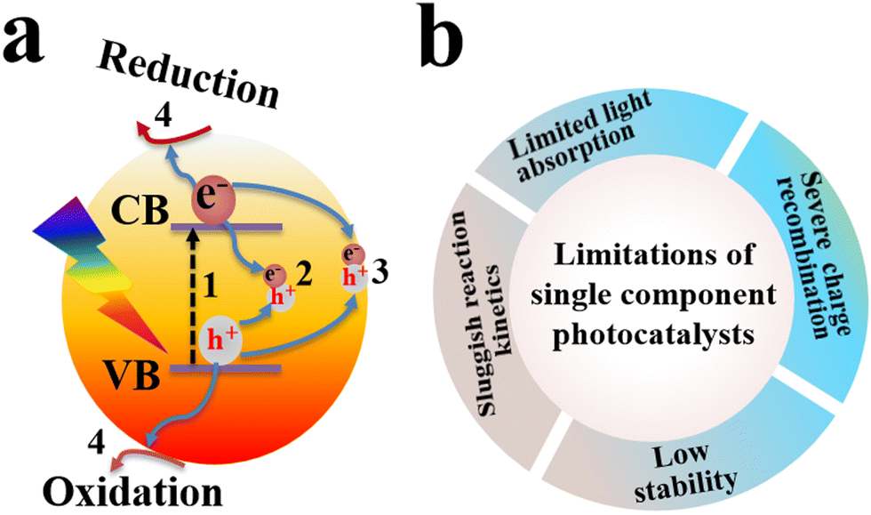 | ||
| Fig. 1 (a) Schematic illustration of photo-based processes that occur after light absorption by a semiconductor. Paths 1–4 represent electron excitation from the VB to the CB leaving behind a hole at the VB, electron–hole recombination within the bulk, electron–hole recombination at the surface, and consumption of separated electrons and holes in the surface reactions, respectively. (b) Limitations of single component photocatalysts. | ||
2. Development of S-scheme photocatalytic mechanisms
Despite the great improvements achieved so far, single-component photocatalysts demonstrate limited photocatalytic activity.8–11 Joining two different semiconductors forming a heterojunction has attracted wide attention from the scientific community due to its potential to diminish charge recombination and steer charge carrier transfer and accumulation at disparate positions for effective consumption for surface redox reactions.12 Various heterojunction configurations, including type-II heterojunctions, and Z- and S-scheme mechanisms, have been employed and developed to mitigate the recombination issue of photogenerated charge carriers in a single photocatalyst and enhance charge separation.11,13,14The charge transfer route of a typical type-II heterojunction is depicted in Fig. 2. After semiconductor 1 (S1) and semiconductor 2 (S2) are excited by light, they generate electrons and holes in their respective CB and VB. Due to the difference in the positions of the CB and VB of S1 and S2, electrons will spontaneously flow from the S2 CB with a higher energy to the S1 CB with a lower energy. Meanwhile, holes will transfer conversely from the S1 VB to the S2 VB (Fig. 2a). Theoretically, these charge transfers can achieve charge separation; however, type-II heterojunctions face thermodynamic, kinetic, and energetic challenges. From a thermodynamic viewpoint, charge migration in type-II heterojunctions results in an unfavorable energy waste because electrons and holes with higher reduction and oxidation potentials are transferred to new positions with lower potentials, respectively, reducing their redox abilities. Moreover, from a kinetic point of view, the strong Coulombic repulsion arising between electrons (in S1 and those transferred from S2) and holes (in S2 and those transferred from S1) should disfavor the transfer and accumulation of a charge carrier onto a disparate semiconductor, which hampers the efficiency of photocatalytic reactions.8 Even more, this transfer is associated with partial energy loss after photogenerated electrons and holes transition from higher to lower energy positions.8–10
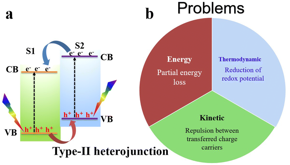 | ||
| Fig. 2 (a) Schematic illustration of the charge transfer route in type-II heterojunctions. CB, VB, S1, and S2 correspond to the conduction band, valence band, semiconductor 1, and semiconductor 2, respectively. (b) Illustration of the limitations of type-II heterojunctions. | ||
Inspired by the natural photosynthesis process, Z-scheme charge transfer modes were also proposed. The traditional Z-scheme, proposed by Bard in 1979,15 involves a liquid-phase redox mediator (e.g., Fe3+/Fe2+), mediating charge transfer and maintaining photogenerated electrons and holes with high redox potential (Fig. 3a, left). Consequently, charge carriers with strong redox abilities are preserved. However, conceptually, this mechanism has several inconsistencies that make its validity doubtful.16 First, the actual charge separation pathway is opposite to the proposed one. Photogenerated electrons at the CB of S2 tend to be transferred to recombine with holes at the VB of S1. Thus, the resulting electrons and holes after charge migration in the heterojunction have the lowest redox potential (Fig. 3a, right). Secondly, the Brownian motion of photocatalyst particles causes continuous movement (Fig. 3b, left), so the distance between S1 and S2 successively changed making charge migration aleatory. Furthermore, the thermal motion of the ionic mediator leads to its random diffusion to other areas, which cannot ensure the position of ions between S1 and S2 (Fig. 3b, middle). Furthermore, most photocatalytic reactions are performed under continuous stirring to ensure disorder in the system. Of note, the Z-scheme system is not in stillness, but in a moving state. These factors make the traditional Z-scheme mechanism problematic and correspond to an inaccurate description of the photocatalytic mechanism (Fig. 3b, right).17
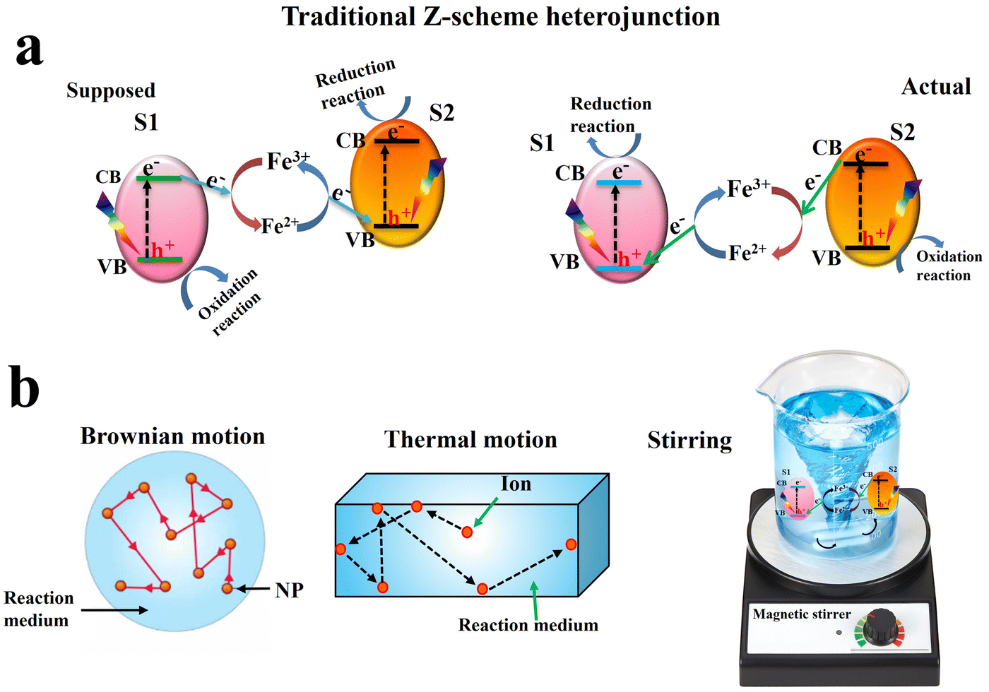 | ||
| Fig. 3 Schematic illustration of the charge transfer route (a) and corresponding problems (b) in traditional Z-scheme heterojunction. | ||
To expand the scope of traditional Z-scheme configurations, the second generation of Z-scheme systems i.e. an all-solid-state Z-scheme, was developed in 2006 by Tada and coworkers.18 In this mechanism, a solid conductor (such as noble metal nanoparticles (Au, Ag), graphene (G), and graphene oxide (GO), etc.) is used as an electron mediator (Fig. 4a, left). Although it has broadened applicability, the all-solid-state Z-scheme mechanism is also wrong from different viewpoints.8,10,16,17 (1) The actual charge transfer direction is still the same as that in traditional Z-schemes. In other words, photogenerated electrons at the CB of S2 should migrate to recombine with holes at the VB of S1. Thus, charge carriers with lower redox potentials are retained (Fig. 4b, right). (2) Since the Fermi level (EF) of most solid conductors is usually lower than that of S1 and S2 (Fig. 4b left), electrons from S1 and S2 will transfer to the conductor after they come into close contact until Fermi levels are aligned. Consequently, a Schottky junction (ΦS) between the solid mediator and S1 or S2 will be formed. Unfortunately, this Schottky junction prevents the continuous transfer of photogenerated electrons from S1 to the mediator and finally to S2 (Fig. 4b right). (3) From a preparation viewpoint, it is challenging to precisely allocate the solid mediator just between the two photocatalysts ca. S1 and S2. Instead, the solid conductor should be randomly deposited over the external surface (Fig. 4c). For these reasons, it is concluded that the assumption of the all-solid-state Z-scheme mechanism raises serious conceptual concerns.16,19
 | ||
| Fig. 4 Schematic illustration of the charge transfer route and corresponding problems in all-solid-state Z-scheme heterojunction systems. (a) Proposed (left) and most probable (right) charge transfer pathway; (b) schematic diagram showing the Schottky junction formation between semiconductors and the solid conductor, before contact (left, EF referring to the Fermi level) and under light (right, Φ refers to the Schottky junction); and (c) an illustration displaying the random distribution of the solid conductor over the external surface of heterojunction components highlighting that only a few of these nanoparticles (NPs) are located properly between S1 and S2 semiconductors. | ||
To tackle the problems of type-II heterojunctions, the third generation of Z-scheme systems, namely the direct Z-scheme mechanism, was first proposed in 2013 by Yu and colleagues.20 For the direct Z-scheme mechanism, no electron mediator is required and S1 and S2 come into close contact. However, since 2019, it has been found that its first and second generations are regarded as problematic and incomplete.16,17,19 Therefore, in 2019, Yu's group again proposed the concept of the Step-scheme (S-scheme) mechanism to describe the charge transfer process over the WO3/g-C3N4 photocatalyst.21
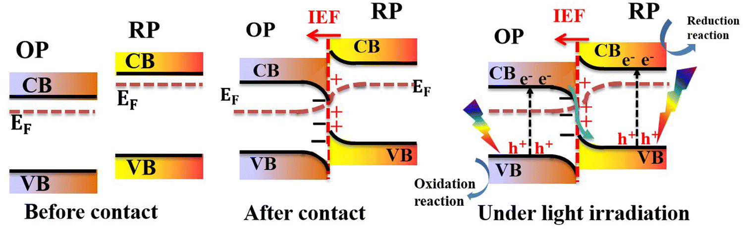
In a typical S-scheme heterojunction system, two semiconductors (namely the reduction photocatalyst (RP) and oxidation photocatalyst (OP)) with staggered band positions come into contact with each other (Fig. 5, left).7,22–24 The RP should possess a higher CB position and Fermi level, while the OP has a relatively lower CB and Fermi level. When both components come into contact, the difference in their work functions culminates in an interfacial electron transfer from the RP to OP. This electron redistribution leads to band bending. Concurrently, the interface region from the RP sides becomes positively charged. Contrarily, the interface region from the OP side becomes negatively charged (Fig. 5, center). Under these circumstances, an internal built-in electric field (IEF) is established at the interface, whose direction points from the RP to OP. Upon light irradiation, electrons are excited from the VB to the CB of each respective photocatalyst. The IEF drives photogenerated electrons from the OP to recombine with holes in the VB of the RP. Meanwhile, useful photogenerated electrons and holes at the RP CB and OP VB with the highest reduction and oxidation potentials are maintained to trigger redox reactions, respectively (Fig. 5, right). The IEF provides a driving force for carrier transfer and separation, thus, regulating their behavior and kinetics. The S-scheme charge transfer mechanism not only realizes charge separation and transfer over the entire system but also suppresses charge recombination within the OP or RP itself thus maintaining their potential for effective redox reactions.7,8,25–28
 | ||
| Fig. 5 Schematic illustration of the charge transfer mechanism in S-scheme heterojunctions. | ||
From the viewpoints of explaining the enhanced photocatalytic activity, maintaining high redox ability of photogenerated charges, and fostering spatial separation of charge carriers and alleviating their detrimental recombination, the S-scheme mechanism presents an adequate conceptual framework for achieving these pursuits. Additionally, S-scheme heterojunction photocatalytic systems have been proven to have promising potential for offsetting the limitation of single component photocatalysts regarding: (i) the severe recombination of photogenerated electron–hole pairs due to the strong Coulombic attraction acting between them. (ii) The limited light absorption and failure to fully utilize the wide spectrum of the solar irradiation. And (iii) the weak redox potential due to limited bandgap size.
In view of the previous considerations, it appears clear that the emergence of S-scheme heterojunctions represents a step forward to a better understanding of charge carrier migration in heterojunctions. The historical development of different concepts of heterojunction photocatalysts is presented in Fig. 6a. Since the foundation of the S-scheme charge transfer concept in 2019, several thousands of research studies have been devoted to the construction and application of S-scheme heterojunctions in the field of photocatalysis.28–30Fig. 6b shows the number of publications on the topic of S-scheme heterojunctions according to the Web of Science database.
 | ||
| Fig. 6 (a) Historical development of concepts to explain heterojunction photocatalysts since the first report on photoelectrocatalytic water splitting by Honda and Fujishima. (b) Number of publications retrieved using the keywords “photocata* and S-scheme” or “photocata* and step-scheme” or “photocata* and s-type” in blue bars and “CuO* and S-scheme” or “Cu2O* and S-scheme” or “CuWO4* and S-scheme” or “CuBi2O4* and S-scheme” or “CuFe2O4* and S-scheme” and so on presented in green bars. The results were obtained from a Web of Science Core Collection search on December 11, 2024. | ||
3. Copper-based photocatalysts in S-scheme heterojunctions
TiO2, ZnO, and g-C3N4 photocatalysts are extensively researched as useful components for S-scheme construction.31,32 In this vein, copper (Cu) is a versatile transition metal with excellent electrical and thermal properties.33,34 With multiple oxidation states and suitable abundance in the Earth's crust, Cu is found in many formulations including pure metallic Cu, oxides (CuO and Cu2O), sulfides (CuxS, (1≤ x ≤ 2)), selenides (CuSe), and basic carbonate (Cu2CO3(OH)2), among others. Of the different oxidation states, Cu(I) and Cu(II) are the most commonly found, showing diverse activity in many catalytic applications.35,36 Regarding photocatalytic applications, Cu-based semiconducting materials are characterized by narrow bandgaps, allowing them to absorb in the visible light region of the solar spectrum with a large absorption coefficient (∼105 cm−1) and suitable band positions.37,38Fig. 7 depicts the bandgap and band positions of the most studied Cu-based photocatalytic materials, along with the benchmark TiO2 and ZnO for comparison. The redox potentials of the most common photocatalytic reactions have also been indicated. Additionally, Table 1 summarizes some of the optical and electronic properties of Cu-based photocatalytic materials discussed in this review.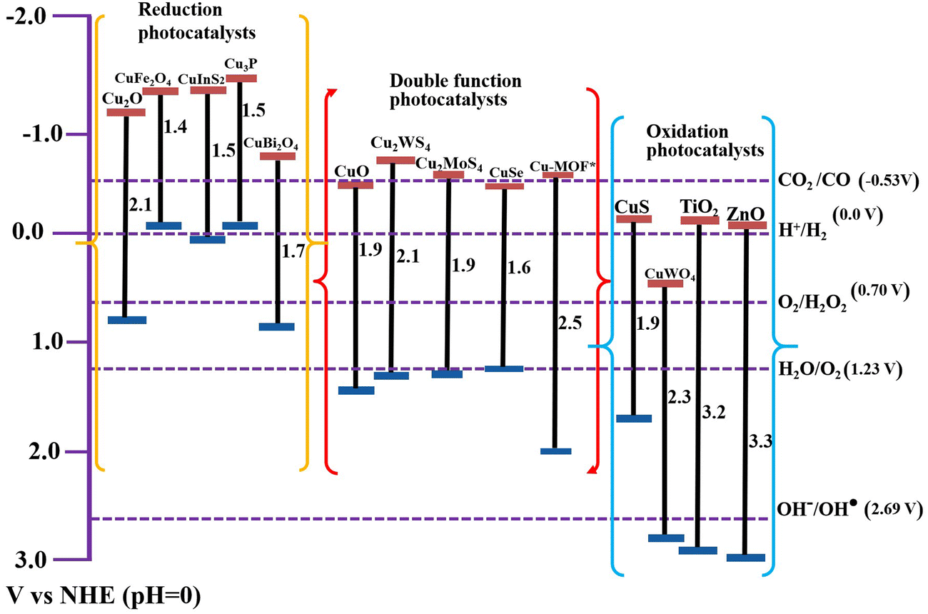 | ||
| Fig. 7 Bandgaps and band positions of the Cu-based photocatalytic materials discussed in this review (as reported in the corresponding references). Benchmark TiO2 and ZnO photocatalysts are provided for comparison. * Cu-MOF refers to the Cu-BTC MOF.39 | ||
| Cu-based photocatalyst | Semiconductor type | Bandgap (eV) | CB position (V vs. NHE, pH = 0) | Work function (eV) |
|---|---|---|---|---|
| Cu2O | p | 2.0–2.2 | −1.2 | 4.9 |
| CuO | p | 1.5–1.9 | −0.4 | 5.5 |
| CuBi2O4 | p | 1.8 | −0.8 | 4.8 |
| CuFe2O4 | p | 1.4 | −1.3 | 5.4 |
| CuWO4 | n | 2.3 | +0.4 | 5.2 |
| CuS | p | 1.9–2.1 | −0.3 | 6.5 |
| CuInS2 | p | 1.5–1.8 | −1.4 | 4.2 |
| Cu2WS4 | n | 2.1 | −0.8 | 5.1 |
| CuSe | p | 1.3–1.6 | −0.4 | 5.1 |
| Cu3P | p | 1.5 | −1.6 | 4.7 |
| Cu-MOF | n | 2.5 | −0.6 | 5.2 |
Due to the aforementioned merits and considering the affordable cost of Cu, Cu-based materials are widely exploited as photocatalytic scaffolds in different applications such as HERs,33,46,47 CO2 reduction,48–50 H2O2 generation,51,52 and pollutant degradation.53–55 In particular, due to their upgraded activity, improved stability, and selectivity, Cu-based S-scheme heterojunction photocatalytic systems are among the preferred materials within the realm of photocatalytic applications. Therefore, their integration into S-scheme heterojunctions has been continuously growing in recent years (Fig. 6b).
Cu-based photocatalytic materials can be categorized as either RPs or OPs according to their electronic structure. However, many members of the family possess suitable band structures to accomplish dual functionality i.e. RP or OP, depending on the accompanying counterpart. Fig. 7 categorizes Cu-based photocatalytic materials on this basis. As can be seen, Cu-based photocatalytic scaffolds present diverse entities whether as RPs or OPs. Yet, all of them exhibit narrow bandgap characteristics. Consequently, these materials represent a variety of choices for constructing efficient S-scheme photocatalytic systems for specific purposes.
Excellent reviews have been devoted to highlighting the synthesis, modification, and integration of Cu-based scaffolds in photocatalytic applications. For instance, Gawande and Goswam comprehensively reviewed the synthesis and modifications of Cu NPs and related nanomaterials and their manipulation in catalysis.35 The recent advances in Cu-based nanocomposite photocatalytic materials for CO2 conversion into solar fuels have also been reviewed.38 Recently, general aspects regarding the synthesis, modifications, and applications of Cu-based photocatalysts have been summarized.33,37 However, a thorough review of recent advances regarding Cu-based S-scheme photocatalytic systems is still missing. Here, we comprehensively discuss up-to-date progress in Cu-based materials including oxides (Cu2O and CuO), binary oxides (CuBi2O4, CuFe2O4 and CuWO4), chalcogenides (CuS, CuSe and Cu-based binary sulfides), Cu–phosphides (Cu3P) and Cu-MOFs, among others, forming part of S-scheme heterojunction photocatalytic systems. As a hot topic in the realm of photocatalysis, design principles and verification approaches for S-scheme heterojunctions will be presented. The synthetic strategies and brief descriptions of characterization data for relevant examples of the aforementioned Cu-based photocatalytic materials will be introduced. Current gaps and future research opportunities will also be provided. We aim to provide a detailed overview of the Cu-based materials that have so far been integrated in S-scheme photocatalytic systems to show the progress in the field to a broad community belonging to different disciplines such as chemical engineering, organic and inorganic chemistry, materials science and solar energy utilization, among others.
4. Design of copper-based S-scheme photocatalysts
In general, a typical S-scheme heterojunction system contains two photocatalytic scaffolds with suitable band structures and close interfacial contact, allowing charge migration following the S-scheme configuration driven by the built-in IEF. Different combinations of OPs and RPs with distinct p- and n-type semiconducting characteristics can fulfill the requisites of S-scheme heterojunction configurations. Generally, four combinations of n- and p-type semiconductors can be integrated to establish S-scheme configurations. These include n–n, p–p, n–p, and p–n heterojunctions. This fact offers multiple choices for constructing S-scheme systems yet all these combinations follow the same charge transfer mechanism. Fig. 8 shows various combinations of n- and p-type semiconductor photocatalysts to construct S-scheme heterojunctions.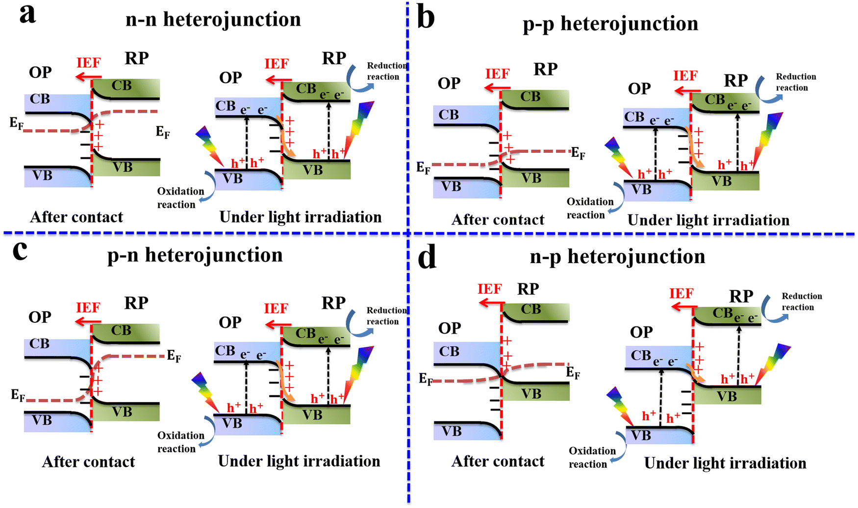 | ||
| Fig. 8 Four types of S-scheme heterojunctions formed between: (a) n–n OP and RP, (b) p–p OP and RP, (c) p–n OP and RP, and (d) n–p OP and RP. In these combinations, electrons are transferred from the RP to the OP after contact. However, after irradiating the system with light, photogenerated electrons are transferred in the opposite direction under the IEF′s driving force. | ||
Consistently in this review, the OP is written first, followed by the RP. For example, in the CuO/In2O3 S-scheme heterojunction, CuO acts as the OP, while In2O3 serves as the RP. Generally, the classification of photocatalytic components in S-scheme heterojunctions into OP and RP relies mainly on their Fermi levels and VB and CB positions. A photocatalyst with a higher Fermi level and CB in the junction will act as the RP where reduction reactions occur. Meanwhile, the other photocatalyst with lower Fermi levels, CB, and VB energy values will be the OP, where oxidation reactions take place. From thermodynamic and kinetic viewpoints, it is desirable to effectively accomplish photocatalytic reactions through S-scheme heterojunctions in which RP and OP possess suitable CB and VB positions i.e. more negative and more positive, respectively. Therefore, photogenerated electrons and holes located at the RP CB and OP VB, respectively, have adequate potential to trigger redox reactions with suitable yields and fast rates.
Table 1 summarizes the semiconducting type, bandgap, CB position, and work function of most Cu-based photocatalysts discussed in this review. Cu-based photocatalytic materials provide versatile choices for designing S-scheme heterojunctions for different target applications. In this context, some Cu photocatalysts can be exclusively RP or OP. Meanwhile, there are still photocatalysts with suitable band positions that exhibit dual functionality depending on the other component in contact.
Beyond the typical requirements to construct S-scheme heterojunctions, the stability of individual components should be considered for effective and practical applications. For instance, Cu2O and CdS are sensitive to surface corrosion by photogenerated holes. Therefore, their integration as a OP in S-scheme heterojunctions is unfavorable from a stability standpoint.
5. Characterization of S-scheme photocatalysts
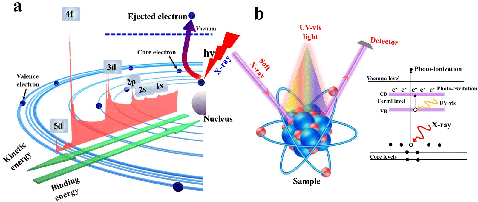
Since the S-scheme charge transfer mechanism describes the process of electron transfer and separation among two combined semiconductors with staggered band positions i.e. OP and RP,10,25,56 diverse tools can be deployed to interpret the existence of such charge movement and space separation. The most adopted approaches so far are ex situ/in situ irradiated X-ray photoelectron spectroscopy (ISIXPS), surface potential measurement, and DFT calculations.7,28 Recently, femtosecond transient absorption spectroscopy (fs-TAS) has emerged as a powerful tool to study the charge transfer dynamics in heterojunction photocatalysts.57 The next sections aim to shed light on these tools, explaining how to confirm the occurrence of S-scheme charge transfer action.5.1. Ex situ/in situ irradiated X-ray photoelectron spectroscopy (ISIXPS)
XPS has been widely utilized to analyze the composition of a material as well as the chemical state of elements. In principle, it is a surface-specific spectroscopic technique based mainly on light–matter interactions. When an X-ray photon with energy higher than the sample ionization impinges into the sample surface (Fig. 9a), it induces the ejection of a core electron with a kinetic energy that is determined by the electron binding energy (BE) of the ejected electron and photon energy (eqn (1)):| Ekinetic = hν − Ebinding | (1) |
 | ||
| Fig. 9 (a) Schematic illustration of the XPS working principle. (b) Illustration of ISIXPS measurements. | ||
The electron BE value is determined by the interplay between two forces i.e. the Coulombic attraction between the nucleus and electrons and Coulombic repulsion among the electrons themselves. Therefore, any change in the element's electronic density and/or valence state will imply a corresponding change in its BE, known as a chemical shift. For a specific element, if the electron density over it increases, its electronic BE decreases. Contrarily, if the electron density decreases, its BE increases.
Within a heterojunction, charge transfer from one semiconductor to another induces an electron density difference with respect to both components individually, which can be probed directly from the change in BE values (ex situ XPS). A positive change in the BE of an element within a given semiconductor implies that electrons move from this semiconductor to the other, and vice versa. In addition, ISIXPS is used to probe the change in BE of constituent elements under the influence of irradiation light compared to in the dark (Fig. 9b). When the heterojunction is irradiated by UV-vis light during XPS measurement, valence electrons are excited from the VB to CB (photo-excitation, Fig. 9b). Photoexcited electrons are distributed across the interface of the heterojunction. Electron migration from one component to the other culminates in electron density depletion and accumulation regions, respectively. This charge gradient will induce BE shifts upon illumination compared to under dark conditions. This measurement can provide direct experimental evidence for the charge transfer within the heterojunction during the photocatalytic reaction. Under these circumstances, BEs of constituent elements that belong to regions of electron deficiency will be shifted to higher values and vice versa. For example, ZnO and CuInS2 can form an S-scheme heterojunction, with the band diagram presented in Fig. 10a.52 Taking into account the higher position of the Fermi level (EF) of CuInS2 compared with that of ZnO, electrons are expected to move from the higher EF to lower EFi.e. from the CuInS2 side to the ZnO side until equilibrium is reached.
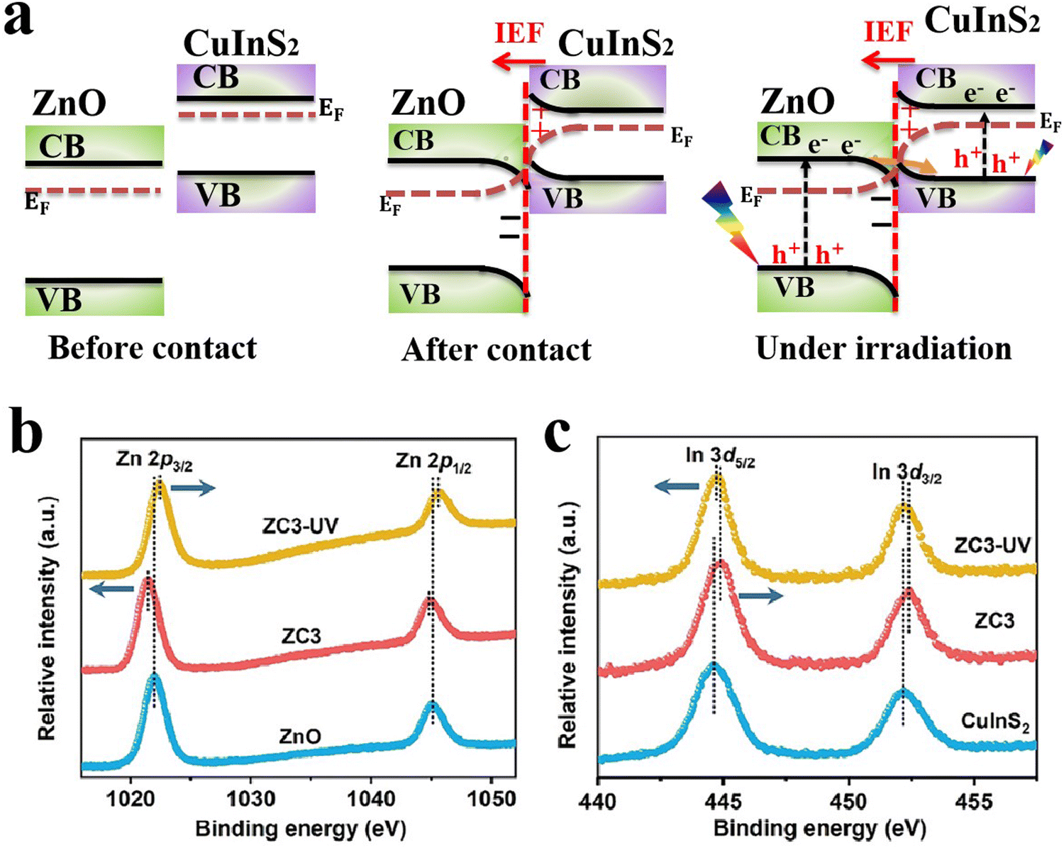 | ||
| Fig. 10 (a) Schematic representation of the band structure of ZnO and CuInS2 and the interfacial electron transfer between them both after contact and under light exposure. Ex situ and ISIXPS spectra of (b) Zn 2p and (c) In 3d recorded for ZnO, CuInS2, and the ZnO/CuInS2 composite in the dark and under UV irradiation. (b) and (c) were reproduced with permission.52 Copyright 2024, Wiley-VCH. | ||
Such electron redistribution will indeed induce a change in the electron density of the elements involved in the process, resulting in a decrease and increase in the electron density over CuInS2 and ZnO, respectively. Thus, the BE of constituent elements will change accordingly. As shown in Fig. 10b and c, the BEs of Zn 2p are shifted toward lower values after contacting CuInS2 compared to pristine ZnO (bottom and middle charts of Fig. 10b). In contrast, the BEs of In 3d are relocated to higher values (bottom and middle plots in Fig. 10c).52 These shifts in BE values confirm that electrons migrate from CuInS2 toward ZnO during hybridization. Under light irradiation, ZnO and CuInS2 will be respectively excited. The photogenerated electrons will transfer in the opposite direction, i.e. from ZnO to CuInS2 under the influence of the IEF (Fig. 10a), resulting in a different electron density change and hence a chemical shift over each component (Fig. 10c). The combined results confirmed that charge is transferred within the ZnO/CuInS2 heterostructure according to the S-scheme mechanism, with electrons moving from the RP (CuInS2) to OP (ZnO) after contact. Meanwhile, photogenerated electrons migrate in the opposite direction under light excitation. The ISIXPS technique has been extensively employed to verify the occurrence of a charge transfer according to the S-scheme configuration in heterojunction photocatalysts.
5.2. Surface potential
Kelvin probe force microscopy (KPFM) is a tool that enables imaging of the surface potential on a broad range of materials at the nanometer scale. It can measure the contact surface potential of the sample (work function) by monitoring the contact potential difference (CPD) between the atomic force microscopy (AFM) tip and the sample (Fig. 11). The CPD between the tip and sample is defined as:58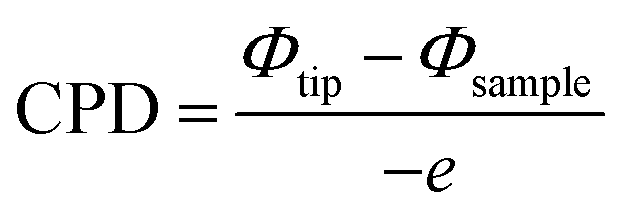 | (2) |
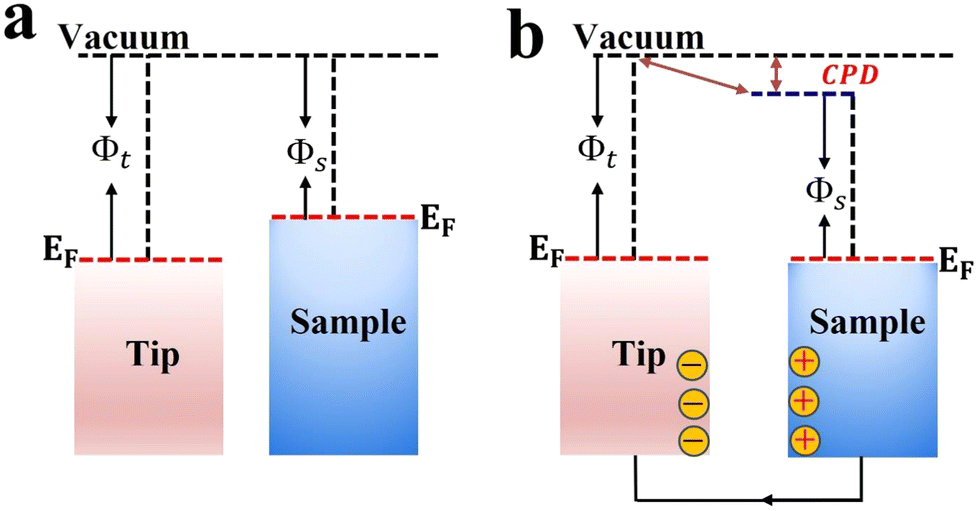 | ||
| Fig. 11 Schematic illustration of the KPFM working principle before (a) and after (b) electrical contact. | ||
For heterojunction systems where charges are distributed between individual components after coming into contact, KPFM can be used to map the potential difference over the composite sample under dark and light conditions. By comparing the CPD of pure components with that of the composite sample in the dark and upon illumination, the redistribution of electron density can be probed. For example, the charge transfer dynamic was investigated over pyrene-alt-dibenzothiophene S,S-dioxide (P16PySO)/WO3 S-scheme heterojunctions using KPFM imaging (Fig. 12).59 The three-dimensional surface potential imaging shows the composite heterojunction (PW10) under dark and light conditions (Fig. 12a). Components A and B in Fig. 12a represent P16PySO and WO3, respectively. Under light, the CPD of WO3 (point B) was significantly increased by 17 mV compared to that in the dark (Fig. 12b). This finding implies that photogenerated electrons migrate from WO3 to P16PySO driven by the built-in IEF in accordance with the S-scheme charge transfer configuration. Given that the work functions of P16PySO and WO3 were calculated to be 4.46 and 4.75 eV, respectively, the charge transfer pathway over the P16PySO/WO3 S-scheme heterojunction can be drawn as in Fig. 12c. In this regard, WO3 and P16PySO serve as the OP and RP in the PW composite.
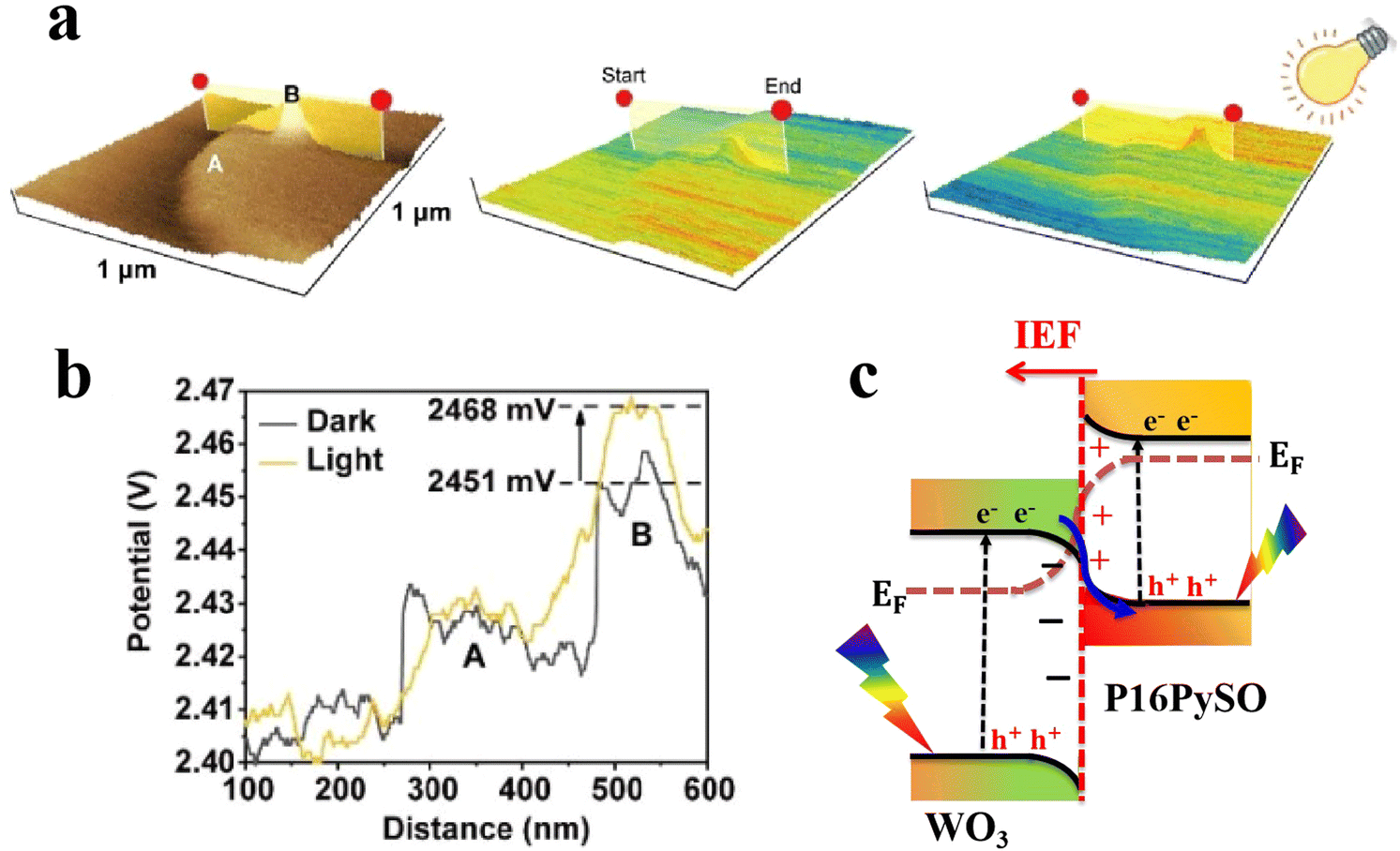 | ||
| Fig. 12 (a) Atomic force microscopic image of PW10 (left), and the 3D KPFM surface potential distribution for PW10 under dark (middle) and light (right) conditions. (b) Corresponding line-scanning of CPD for PW10 in the dark and under light.59 Reproduced with permission. Copyright 2023, American Chemical Society. (c) Band structure and proposed charge transfer pathway over the P16PySO/WO3 S-scheme heterojunction. | ||
Generally, CPD is a suitable technique to predict charge movement between semiconducting components in S-scheme heterojunction photocatalysts.
5.3. Density functional theory (DFT) simulations
The charge density is a core quantity in DFT calculations and it can be utilized for different aspects of materials science from bonding to determining charge transfer between specific atoms.60 In photocatalytic heterojunctions, DFT simulations have been extensively utilized to elucidate the charge density difference across the heterojunction interface. The results predict the differential electrostatic potential along a perpendicular plane to the heterojunction surface based on charge distribution between the components across the interface. In this vein, charge will flow from a material with a lower work function to another with a higher work function. As an example, the charge density difference across the CuFe2O4/ZnIn2S4 interface heterojunction has been simulated (Fig. 13). The work functions of CuFe2O4 (Φ = 5.36) and ZnIn2S4 (Φ = 6.74) were calculated based on DFT principles. Fig. 13a depicts band structures for both components. After contact, due to the difference in the Fermi levels, electrons are transferred from CuFe2O4 to ZnIn2S4. As a result, electron depletion (cyan area) and accumulation (yellow area) regions are found on CuFe2O4 and ZnIn2S4 sides, respectively (Fig. 13b). The Bader charge analysis results (Fig. 13c) indicated the transfer of 0.75e− per molecule from CuFe2O4 to ZnIn2S4 through the interface, further demonstrating the unique charge transfer mechanism.61 Validation of DFT theoretical calculations with experimental data has confirmed DFT as a powerful tool for predicting the charge distribution across the heterojunction interface. Besides, the assignment of active sites and determination of reaction mechanisms and kinetics have become feasible theoretical tasks.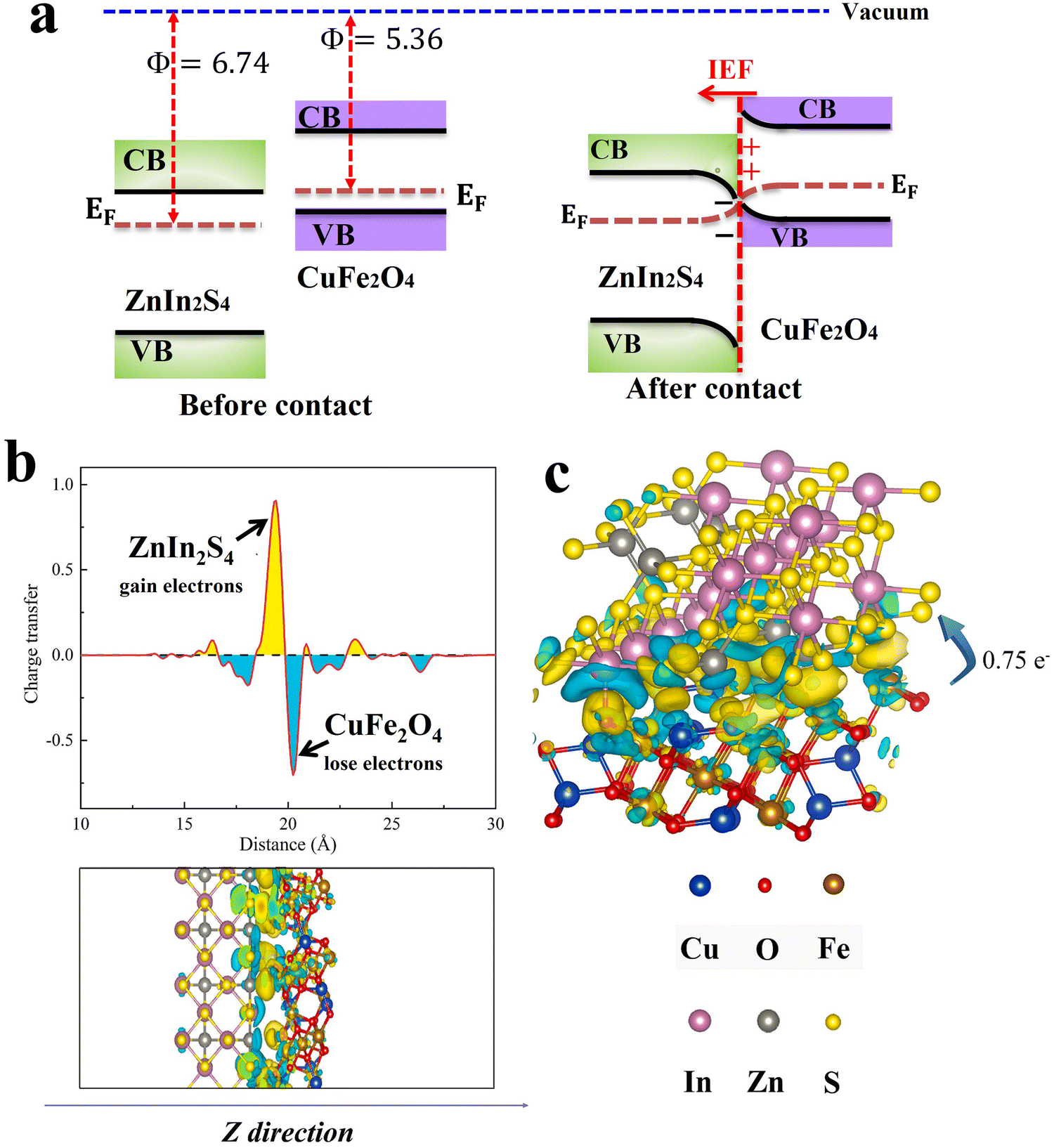 | ||
| Fig. 13 (a) Schematic illustration of band structure and charge transfer between CuFe2O4 and ZnIn2S4. (b) The plane average charge density difference and Z-direction differential charge density map. (c) The differential charge density map, where the yellow and cyan electron clouds represent enhanced and depleted electron density with respect to the individual components. Reproduced with permission.61 Copyright 2024. Elsevier. | ||
5.4. Femtosecond transient absorption spectroscopy (fs-TAS)
Fs-TAS is a powerful technique for monitoring the dynamics of photogenerated electrons and holes in heterojunction photocatalysts.57 The time-resolved spectroscopic technique is adopted to explore the relaxation pathways of excitons on a picosecond-to-femtosecond time scale and measure the lifetime of photogenerated electrons and/or holes after their generation. A typical fs-TAS spectrophotometer consists of four main parts ca. a laser source, optical parametric amplifier (OPA), delay system, and detector (Fig. 14). In detail, a conventional femtosecond Ti–sapphire laser source produces laser pulses of 800 nm. This main beam is split into two beams viz. a pump beam and a probe beam. The pump beam is converted into shorter wavelengths (320–700 nm) by the OPA and passes through a computerized optical chopper before exciting the target sample. The probe beam is delayed by a computer-controlled delay system and then focused on a sapphire crystal to generate a white light continuum that hits the sample cell. After passing through the sample, the transmitted white light beam is collected on the detector, while the pump beam is blocked. The pump beam reaches the sample first, causing the excitation of electrons from the ground state to the excited state. After being delayed, the probe white-light beam reaches the samples after a specific delay time with respect to the pump. Ground state and excitons (instantaneously generated by the pump pulse) can absorb some wavelengths of the probe pulse. The differential transient absorption (ΔA) spectra of the sample are obtained by measuring the absorption caused by the probe pulse with and without pump pulse excitation, respectively. By changing the delay time, the number of excited states will also change, and so will ΔA. Therefore, the lifetime of charge carriers can be obtained by fitting the transient signal decay to first order or other kinetics equations.57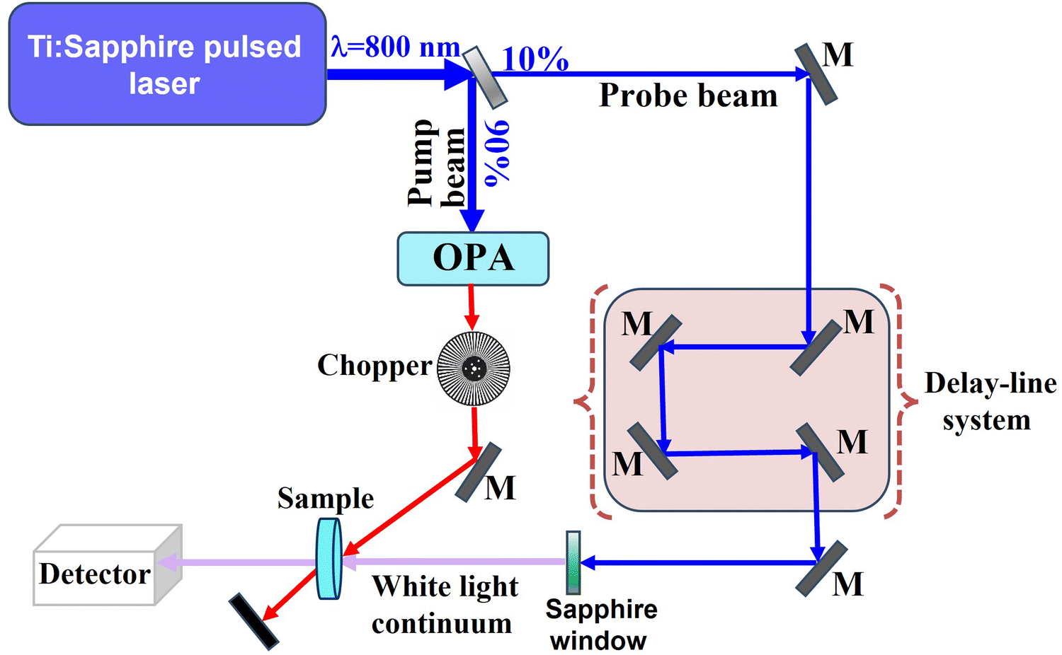 | ||
| Fig. 14 Schematic layout of the fs-TAS apparatus setup. M: mirror; OPA: optical parametric amplifier. | ||
For photocatalytic heterojunctions, the process of electron transfer across the interface can be supported by two features from fs-TAS analysis in comparison to the individual components. Firstly, a new relaxation pathway with an ultrafast lifetime exists within the spectrum of the heterojunction that is absent in the spectra of the pure components.62 Secondly, the lifetime of a specific charge carrier becomes longer after integrating within a heterojunction system. Observation of these two features implies that the target exciton is effectively separated across the interface, thereby providing spectroscopic evidence in support of the charge transfer step.63
For example, the electron transfer process in the TiO2/Bi2O3 heterojunction system was investigated by fs-TAS measurements performed on TiO2 (TO) and TiO2/Bi2O3 (TBO40, 40 represents the wt% of Bi2O3).62Fig. 15a and b depict the ground state bleaching (GSB) peak at λ ∼ 395 nm and the excited state absorption (ESA) peak at λ ∼ 425–550 nm in both TO and TBO40. The authors also recorded the fs-TAS spectra of TO with an electron scavenger (AgNO3) to resolve the contributions from both excitons. According to the fitting results of GSB recovery kinetics (Fig. 15c), the τave values of holes increase from 148.5 ps for TO–AgNO3 to 232.5 ps for TBO40. The longer lifetime of photogenerated holes on the composite TBO40 than that in pure TO – even with an electron scavenger – implies the occurrence of an efficient electron transfer from TO (as OP) to BO (as RP) through an interfacial electron transfer from the CB of TiO2 to the VB of Bi2O3 according to an S-scheme mechanism (Fig. 15d). The emergence of new relaxation pathways was also reported for the In2O3/Nb2O5 heterojunction.64 Generally, fs-TAS is a direct approach to probe the charge dynamics in S-scheme heterojunction photocatalysts. The emergence of a new relaxation pathway or the prolongation of the average lifetime of excitons is directly related to their possible separation and transfer across the interface.
 | ||
| Fig. 15 fs-TAS of TiO2 (TO, a) and TiO2/Bi2O3-40 (TBO40, b) recorded with 340 nm excitation. (c) Corresponding fit of the transient absorption kinetics for TO-AgNO3 and TBO40 monitoring at 395 nm within a time window of 100 ps. Reproduced with permission.62 Copyright 2022, Wiley-VCH. (d) Schematic illustration of S-scheme charge transfer within the TBO40. | ||
6. Construction of Cu-based S-scheme photocatalysts
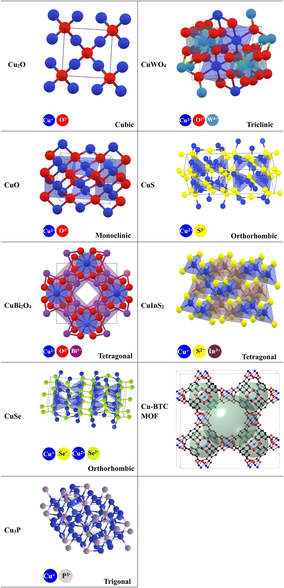
Various Cu-based photocatalytic materials described in the literature within the last four years as forming S-scheme heterojunctions will be thoroughly discussed, including Cu–oxides, Cu–binary oxides, Cu–chalcogenides, Cu–phosphides, and Cu–MOFs. These compounds possess fascinating structural, optical, and electronic properties. Additionally, they showed promising photocatalytic activity. The crystal structures of these compounds are given in Table 2.
|
6.1. Cu-based oxides
This group includes Cu2O, CuO, and Cu-based binary oxides. The next sections will discuss their integration into S-scheme heterojunctions with different photocatalytic scaffolds.| S-scheme heterojunction | Application | Efficiency | Ref. |
|---|---|---|---|
| CuO/Cu2O | CO2 reduction | CO yield = 22.14 μmol g−1 h−1 | 65 |
| CuO/Cu2O | Methyl orange (MO) degradation and Cr(VI) reduction | Degradation = 96 and 81.8% for MO (20 min) and Cr(VI) (40 min), respectively | 66 |
| TiO2/Cu2O | 4-CP degradation | 100% degradation in 40 min | 67 |
| TiO2/Cu2O | H2 evolution | Evolution rate = 13![[thin space (1/6-em)]](https://www.rsc.org/images/entities/char_2009.gif) 521.9 μmol g−1 h−1 521.9 μmol g−1 h−1 |
68 |
| ZnO/Cu2O | H2 evolution | Evolution rate = 209 μmol g−1 h−1 | 69 |
| ZnO/Cu2O | Doxycycline hydrochloride (DCHCl) degradation and Cr(VI) reduction | Degradation = 92.9 and 88.9% for DCHCl and Cr(VI) in 90 min, respectively | 70 |
| WO3/Cu2O | Carbamazepine (CBZ) degradation and nitrobenzene (NB) reduction | 94% CBZ degradation in 60 min and 88% photoreduction of NB into aniline was achieved in 150 min | 71 |
| WO3/Cu2O | Degradation of levofloxacin (LVX) | 97.9% LVX degradation in 80 min | 72 |
| WO3/Cu2O | CO2 photoreduction | CH4 yield of 1.87 mmol g−1 within 18 h | 73 |
| W18O49/Cu2O | N2 fixation | NH3 yield of 252.4 μmol g−1 h−1 | 74 |
| Cu2O/CeO2 | H2 evolution | ∼100 μmol/5 h | 75 |
| CeO2/Cu2O | VOC degradation | Toluene, xylene and formaldehyde completely degraded in 70, 50 and 6 min, respectively | 76 |
| Fe2O3/Cu2O | Benzyl amine (BA) oxidative coupling | Yield = 69.3%, after 6 h | 77 |
| Ag2O/Cu2O | E. coli disinfection | 100% inactivation in 75 min | 78 |
| BiVO4/Cu2O | H2O2 generation | H2O2 yield of 112 μmol L−1 h−1 | 79 |
| Bi2WO6/Cu2O | Water oxidation | O2 yield of 50 μmol L−1 within 3 h | 80 |
| BiOBr/Cu2O | CO2 reduction | CH4 yield = 22.78 μmol g−1 within 4 h | 81 |
| BiOBr/Cu2O | Methylene blue (MB), rhodamine B (RhB), Congo red (CR), methyl viologen (MV) and tetracycline (TC) degradation | Degradation for RhB = 82.33%, CR = 94.57%, MV = 85.88% and TC = 99.59% | 82 |
| BiOBr/Cu2O | TC degradation and Cr(VI) reduction | Degradation = 80.17 and 80.71% for TC and Cr(VI) within 100 min, respectively | 83 |
| BiOI/Cu2O | CO2 photoreduction | CO and CH4 yields = 53.03 and 30.75 μmol m−2, respectively, after 11 h | 84 |
| Cu2O/Mn-doped CdS | H2 evolution | 66.3 mmol g−1 h−1 | 85 |
| Cu2O/CdS | H2 evolution | 12366 μmol h−1 g−1 |
86 |
| ReS2/Cu2O | CO2 photoreduction | CO yield of 14.3 μmol g−1 within 3 h | 87 |
| Cu2O/g-C3N4 | TC degradation and Cr(VI) reduction | TC degradation = 95.1% and Cr(VI) reduction = 77.7% within 120 min | 88 |
| Cu2O/g-C3N4 | CO2 photoreduction | CO and CH4 yield of 10.8 and 3.1 μmol g−1 h−1, respectively | 89 |
| Cu2O/g-C3N4 | H2 evolution and oxytetracycline hydrochloride (OTH) degradation | OTH removal of 94.8% after 120 min. H2 evolution rate = 552.6 μmol g−1 h−1 | 90 |
| g-C3N4/Cu2O | CO2 photoreduction and H2O2 generation | CO and H2O2 yield = 14.6 and 34.0 μmol mg−1 within 2 h | 91 |
| Cu2O/CQDs | TC degradation | TC degradation = 92.49% within 100 min | 92 |
6.1.1.1. Cu2O/metal oxide S-scheme heterojunctions. Cu2O can be combined with a wide range of metal oxides, such as CuO,65,66 TiO2,67,68 ZnO,69,70 WO3,71,72 W18O49,74 Fe2O377 and CeO2,75,76 to form desirable S-scheme heterojunctions. For instance, when Cu2O is combined with Ti3+-doped TiO2, a robust structure with improved activity and stability is obtained.67 The Cu2O/TiO2 S-scheme photocatalyst showed almost 100% degradation of 4-chlorophenol (4-CP) in 40 minutes, with a reaction rate ca. 510 times that of pristine Cu2O and TiO2. The improved activity and stability were attributed to enhanced charge separation thanks to the S-scheme configuration that promotes interfacial charge transfer at the interface. Table 3 summarizes most reported S-scheme heterojunctions involving Cu2O as a photocatalytic component for different applications.
The process of charge separation can be further strengthened after compositing the S-scheme system with cocatalysts or conductive additives such as carbonaceous materials (graphene,78 carbon quantum dots (CQDs), N-doped carbon (NC)68,70), metallic species66,73,93 and MXenes.86 For example, Huang et al.,68 found that the introduction of an NC-layer not only adjusted the Fermi level of TiO2, thus switching the interfacial charge transfer pathway from a p–n to S-scheme heterojunction, but also provided an accessible channel for effective charge separation and transfer. Additionally, metallic Ni was photodeposited over the TiO2–NC–Cu2O composite to serve as an electron sink. The highest photocatalytic H2 evolution rate of 13522 μmol g−1 h−1 was attained for the composite sample containing the optimum percentage of NC and Ni, ca. 664 times higher than that of pure Cu2O. The TiO2–NC–Cu2O–Ni S-scheme system exhibited poor stability, with ∼15% activity loss after 5 cycling tests. The authors employed ISIXPS to confirm the S-scheme charge transfer mechanism. Distinct peak shifts were observed for both Ti 2p and Cu 2p core levels in high-resolution XPS (Fig. 16a and b). Following a typical S-scheme charge transfer mechanism, charges are distributed at the interface after contact and hence an IEF is generated at the interface (Fig. 16c). Under light irradiation, photogenerated electrons at the TiO2 CB are transferred driven by the built-in IEF, to recombine with photogenerated holes at the Cu2O VB. Such charge transfer under illumination imparts corresponding shifts in Ti 2p and Cu 2p XPS peaks to higher and lower binding energies, respectively (Fig. 16a and b). Meanwhile, electrons at the Cu2O CB and holes at the TiO2 VB are maintained being responsible for reduction and oxidation reactions, respectively. Ni metallic species act as reservoirs to accumulate electrons from the Cu2O CB to boost the hydrogen evolution reaction.68 A similar function as an electron accumulation center was reported for Ag NPs deposited over a Cu2O/CuO S-scheme heterojunction during methyl orange (MO) dye degradation and Cr(VI) reduction.66
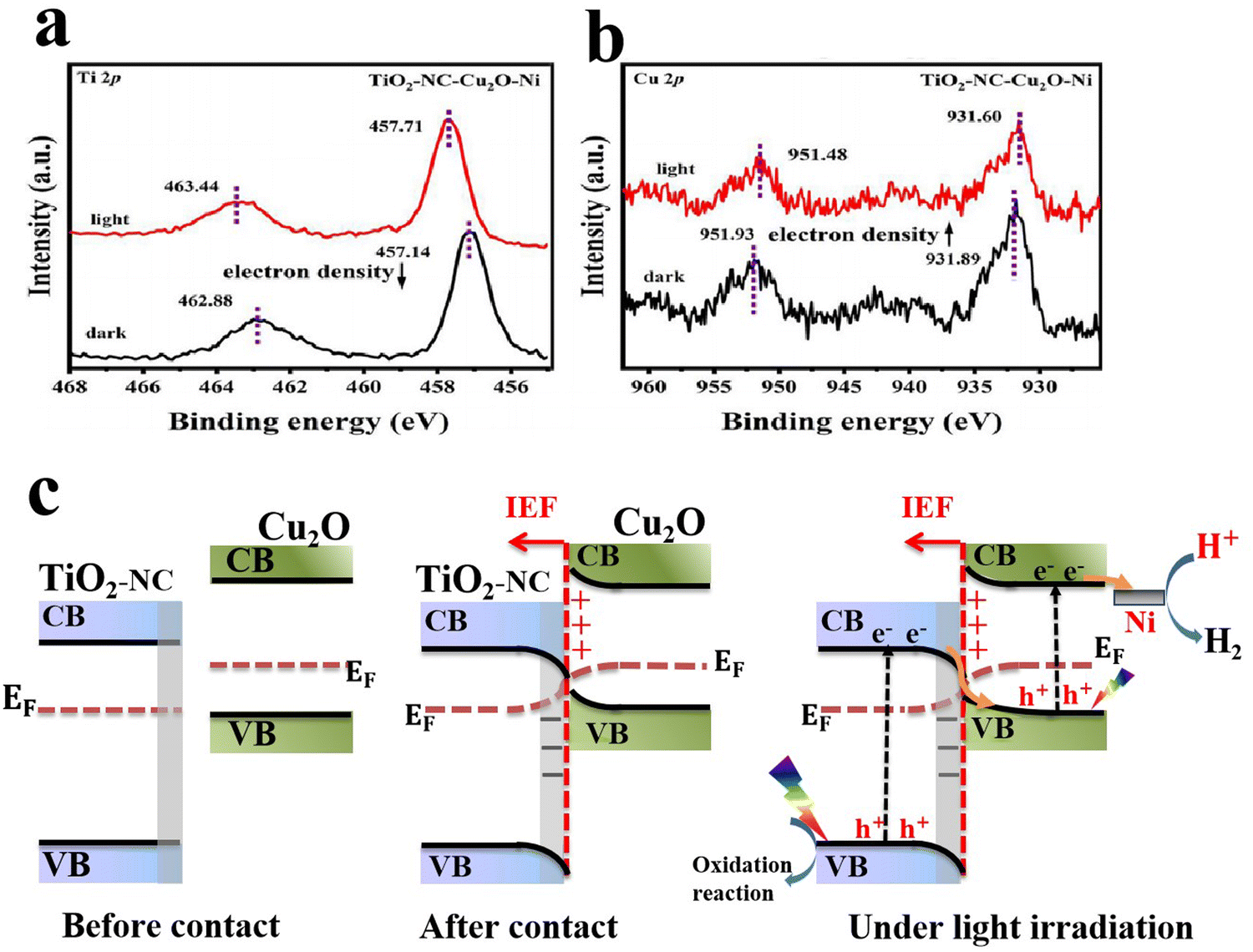 | ||
| Fig. 16 (a) ISIXPS spectra of (c) Ti 2p and (b) Cu 2p for the TiO2-NC-3%Cu2O-3%Ni catalyst in the dark as well as under 365 nm light irradiation. Reproduced with permission.68 Copyright 2024, Elsevier. (c) Schematic representation of interfacial electron transfer and migration over TiO2-NC and Cu2O before contact (left), after contact (middle), and under light irradiation (right). | ||
In light of these studies, conductive cocatalysts with excellent charge transfer ability and minimal photogenerated electron–hole pair recombination were found to dramatically enhance the charge separation over S-scheme heterojunctions, boosting further the photocatalytic activity. On the other hand, establishing a strong interaction and mixing electronic states of individual components greatly improves charge carrier migration and their subsequent separation.
In particular, forming a continuous interface through a chemical bond dangling between the two components creates an accessible channel for barrier-less charge transfer.94 In this vein, interfacial Cu(II)–O–Cu(I) bonding bridges are formed at the interface of Cu2O and CuO, providing appropriate channels for photogenerated carrier transfer from CuO to Cu2O in an S-scheme pathway.65 The Cu(II)–O–Cu(I) bridge channels were constructed via an in situ reduction strategy. In this approach, preformed CuO nanosheets are partially reduced in a controllable manner by ascorbic acid and transformed into Cu2O entities. Such interfacial bonding not only improves the thermodynamics of the CO2-to-CO conversion process but also accelerates the reaction kinetics by altering the rate-determining step through modulation of the d-band center of the Cu(I) sites.
Favored by these interfacial bridges and the S-scheme mechanism, the optimized CuO/Cu2O exhibited improved CO2 photoreduction to CO with a conversion rate of 22.14 μmol g−1 h−1, which is 43.5 and 15.4 times higher than that of pristine CuO and Cu2O, respectively.66
It seems that the in situ reduction strategy has promising potential for establishing strong interaction and electronic state mixing at the interface of individual components. Inspired by this technique, Cui and coworkers74 deposited ultrafine Cu2O NPs over different morphologies of W18O49 and used the composite photocatalysts for N2 photoreduction. Cu2O–W18O49 with ultrathin nanowire morphology exhibited the best NH3 production rate of 252.4 μmol g−1 h−1, which is 11.8 times higher than that of the pristine W18O49. The strong interface bonding with abundant oxygen vacancies promotes the chemisorption and activation of N2 molecules. Besides this attribute, the S-scheme heterojunction enhances the IEF and improves the separation and transfer of the photogenerated carriers, which were considered responsible for the observed activity enhancement.
It is clear that the integration of Cu2O with metal oxide photocatalysts to construct S-scheme heterojunction photocatalysts not only promotes the charge separation at the interface and constrains the electron/hole pair recombination, but also boosts the reaction efficiency by maintaining useful charge carriers with maximum potential to trigger redox reactions and also alleviates the photo-corrosion issue of Cu2O. In light of these studies, Cu2O was chosen as the RP in the S-scheme heterojunction to avoid the accumulation of photogenerated holes within its VB, thus circumventing the photo-corrosion issue. Further loading of conductive cocatalysts and tailoring the interface with interfacial bonding has considerable potential to foster the charges’ transfer and quench their recombination, thus enhancing the overall photocatalytic efficiency.
6.1.1.2. Cu2O/binary metal oxide S-scheme heterojunctions. Similar to metal oxides, Cu2O can form S-heterojunctions with a wide range of binary metal oxides such as BiVO4,79 Bi2WO6,80 and MgFe2O4,95etc. For instance, Huang et al., synthesized single-crystal BiVO4 with exposed (010) facets to achieve directional charge transfer and minimize bulk charge recombination. Subsequently, Cu2O nanoparticles were grown by photodeposition technique along the (010) plane of BiVO4 to construct an S-scheme heterojunction photocatalyst (Fig. 17a–c). MnOOH was loaded on the BiVO4 (110) surface as a cocatalyst.79 The best photocatalyst MnOOH/BiVO4/Cu2O exhibited the maximum H2O2 production performance of 112 μmol L−1, ca. 3.5 times higher than that of BiVO4/Cu2O. However, the activity declined by 20% after the fifth recycling test. Since the work function of Cu2O is smaller than that of BiVO4, electrons flow from Cu2O to BiVO4 at the interface after contact. Therefore, an IEF is established at the interface, in the direction from Cu2O to BiVO4 (Fig. 17d). Under light irradiation, photogenerated electrons and holes from BiVO4 move selectively toward the (010) and (110) facets, respectively. The transferred electrons recombine with holes from Cu2O. Meanwhile, photogenerated electrons at the Cu2O CB and holes from BiVO4 at the (110) facets effectively drive the overall H2O2 generation (Fig. 17d).
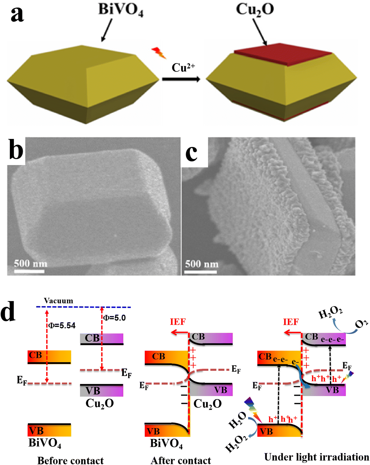 | ||
| Fig. 17 (a) Scheme illustrating the preparation of the BiVO4/Cu2O S-scheme heterojunction. FESEM images of (b) BiVO4 with exposed {010} and {110} facets and (c) BiVO4/Cu2O, where Cu2O is grown selectively over the {010} facets. Reproduced with permission.79 Copyright 2024, Royal Society of Chemistry. (d) Schematic illustration of the charge transfer mechanism over the BiVO4/Cu2O photocatalyst. | ||
Delicate control over structural features such as facets, edges, and defects could open new pathways for further thwarting the unwanted charge carrier recombination. It is believed that these features could help establish a localized built-in electric field that boosts the charge separation process according to the S-scheme migration pathway. Careful consideration should be given to the stability issue of Cu2O-based S-scheme photocatalysts.
6.1.1.3. Cu2O/bismuth oxyhalide S-scheme heterojunctions. Bismuth-based oxyhalides [BiOmXn] (X = F, Cl, Br, and I) represent a versatile category of layered structural materials with unique crystal and electronic structures, and exhibit interesting photocatalytic activity and stability. The layered crystal structure endows them with minimized electron–hole recombination and compositional flexibilities for bandgap tuning.96 All these merits grant bismuth-based oxyhalide materials widespread usage in photocatalytic applications such as pollutant remediation, H2 evolution, CO2 reduction, and N2 fixation.97–99 In this regard, Cu2O has been used to construct S-scheme heterojunctions with different varieties of BiOX including BiOBr,81,82,100 BiOCl83 and BiOI.84
BiOX possesses a variable bandgap of ∼3.3 eV for BiOCl, 2.7 eV for BiOBr, and 1.8 eV for BiOI.98 Due to the anisotropic structural, optical, and electrical properties of BiOX materials, their semiconducting nature is dramatically affected by the composition, preparation method, starting precursor, and doping level. Therefore, they can exhibit p- or n-type semiconducting properties.96,98,101–106 Cu2O can form S-scheme heterojunctions with BiOX photocatalysts regardless of their semiconducting nature, provided that the conditions for an S-scheme configuration are met, as shown in Fig. 8. For instance, Yan et al.,81 fabricated BiOBr/Cu2O using a hydrothermal method for CO2 photoreduction. The prepared composite samples showed moderate activity for CH4 production with a selectivity of about 51%, while pure components produced CO only. The S-scheme configuration promotes the photogenerated electron–hole separation, thus accumulating photogenerated electrons at the Cu2O CB to trigger CO2 reduction to CH4 (8e− per CH4 molecule).
In another study, Gao and coworkers reported the fabrication and manipulation of BiOBr/Cu2O S-scheme photocatalysts for various organic dye degradation processes.82 BiOBr nanosheets (NSs) were prepared using hydrothermal synthesis. Afterward, Cu2O NPs were in situ generated over BiOBr NSs using typical alkali deposition followed by a reduction step. The composite photocatalyst, under the S-scheme mechanism operation, afforded high degradation efficiency for all targeted pollutants. Under light, photogenerated electrons in the BiOBr CB migrate to recombine with holes in the Cu2O VB. Meanwhile, holes with a strong oxidation ability are located in the more positive position i.e. the VB of BiOBr, and are used directly to degrade organic contaminants or produce ˙OH from water oxidation. On the other hand, the electrons at the more negative position i.e. the CB of Cu2O are consumed partially for O2 reduction to H2O2 (Fig. 18a). Under these circumstances, Cu(I) plays an additional role in activating the conversion of produced H2O2 into ˙OH, via a Fenton-like process (Fig. 18a). Then, a portion of the photogenerated electrons at the Cu2O CB are used to partially restore the initial Cu(I) species to sustain the S-scheme photocatalytic action. However, a 40% decrease in activity was observed after the fourth cycle of the recycling tests (Fig. 18b). When glucose was introduced into the system as a reducing agent, the activity was promoted from 60% to 90% (Fig. 18b). These results indicated that the photoreduction (without glucose) is not adequate to fully restore Cu(I). These findings highlight the role of Cu(I) species in activating a Fenton-like process and the possibility of integrating light-switching ionizable cocatalysts during photocatalytic processes. Further attempts to fully restore the Cu(I) species with the aid of the photogenerated charge carriers after a successful photocatalytic reaction without the need for external chemical reducing or oxidizing agents are highly encouraged. The effectiveness of Cu2O/BiOX S-scheme photocatalysts has been again testified for the tetracycline degradation over BiOCl/Cu2O.83
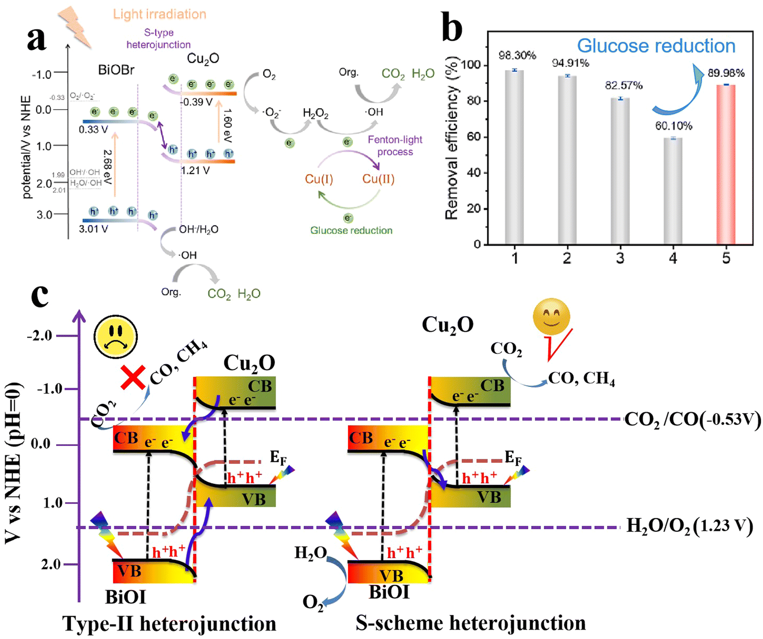 | ||
| Fig. 18 (a) Schematic illustration of the synergism between a S-scheme heterojunction and a Fenton-like reaction over a Cu2O/BiOBr photocatalyst. (b) The photocatalytic degradation efficiency of Cu2O/BiOBr for MB decolorization after four cycles and glucose reduction. Reproduced with permission.82 Copyright 2023, Elsevier. (c) Comparison of type II heterojunctions (left) and the S-scheme mode (right) of photogenerated electron–hole migration in BiOI/Cu2O composites. | ||
Apart from particulate photocatalysts, Wang and coworkers synthesized polyhedral Cu2O-modified BiOI NS thin film S-scheme photocatalysts over a fluorine-doped tin oxide substrate via a stepwise electrodeposition technique and the supported Cu2O/BiOI thin film used for CO2 photoreduction.84
The photocatalyst with optimal Cu2O loading (BiOI/Cu2O-1500, where 1500 refers to the electrodeposition cycles) exhibited improved CO2 reduction ability, producing CO and CH4 as the final reduction products, while oxygen was detected as an oxidation product. It was concluded that the S-scheme heterojunction formed at the BiOI/Cu2O interface imparted the prepared catalyst with improved charge separation and photogenerated carriers with strong redox ability, which collaboratively led to enhanced photocatalytic performance. Specifically, the bandgaps (Eg) of the BiOI and Cu2O samples were estimated to be 1.8 and 2.0 eV, respectively. The VB values of BiOI and Cu2O were estimated to be 1.9 and 0.8 eV. Then, the CB positions of BiOI and Cu2O were determined to be 0.1 and −1.2 V, respectively. Upon visible-light irradiation, according to the charge transfer principles of the S-scheme configuration, photogenerated electrons in the CB of BiOI will migrate under the influence of the IEF to recombine with holes within the Cu2O VB.84 Simultaneously, the accumulated electrons at the CB of Cu2O with the reduction potential (−1.2 V vs. NHE), greater than the standard redox potential E° of CO2/CO (−0.5 V vs. NHE) and E° of CO2/CH4 (−0.24 V vs. NHE), drive these half-reactions at varying rates (Fig. 18c). Meanwhile, O2 production occurs via photogenerated holes at the VB edge of BiOI (1.9 V vs. NHE) as its oxidation potential exceeds the standard redox potential for H2O oxidation (O2/H2O = 1.23 V vs. NHE) (Fig. 18c-right). These results cannot be explained by a type-II heterojunction mechanism, as photogenerated electrons and holes would accumulate in the CB and VB of BiOI and Cu2O, respectively, with reduction and oxidation potentials insufficient to achieve the targeted reactions (Fig. 18c-left).
6.1.1.4. Cu2O/metal sulfide S-scheme heterojunctions. Metal sulfide (MS) photocatalysts have received enormous research interest due to their suitable band structure and promising photocatalytic performance. Compared to metal oxides, MS generally possesses a narrower bandgap and considerable visible light absorption ability.107 CdS, MoS2, Ag2S, and Bi2S3 are among the most studied MS photocatalytic materials. However, the severe charge recombination and pronounced photo-corrosion hinder the efficiency of MS when used as a single-component photocatalyst, particularly CdS. Recently, transition-metal-substituted CdS solid solutions (MxCd1−xS) have been developed to enhance the photocatalytic performance of CdS, while diminishing the use of highly toxic Cd2+.85,94 Theoretically, the doped transition metal ions can induce spin–orbit coupling and hybridization with the electronic states of CdS, thereby shifting the CB position to more negative values, which favors reduction reactions such as H2 evolution and CO2 reduction. When combined with a suitable alternative to construct an S-scheme heterojunction, the resulting composite shows prospective catalytic efficiency. Based on these attributes, Fan et al.,85 deposited Mn-doped CdS onto Cu2O truncated octahedra via hydrothermal synthesis targeting photocatalytic H2 evolution. The S-scheme Mn-doped CdS/Cu2O photocatalyst exhibited outstanding H2 evolution activity that is 3.4 and 55.3 times that of Mn-CdS and Cu2O, respectively, and excellent stability during cycling. Upon Mn-doping, the CB of CdS shifted to a higher position, thereby promoting the H2 evolution reaction, particularly after constructing the S-scheme heterojunction with Cu2O.
MXenes have emerged as a rising star in the 2D materials arena and received considerable interest due to their unique physicochemical properties. In photocatalysis, MXene's excellent electrical conductivity and light absorption ability enable fast photogenerated charge carrier transfer and enhance photocatalytic conversion efficiency.108,109 When combined in an S-scheme heterojunction system, MXene can provide alternative charge transfer channels and abundant active sites, which are collectively essential for accelerating the photocatalytic reaction kinetics.86,110,111 Benefiting from these features, an S-scheme heterojunction system combining CdS and Ti3C2 MXene and coupled with Cu2O was constructed for photocatalytic H2 evolution reaction.86 The synthesis route starts by CdS epitaxial and uniform growth on both surfaces of Ti3C2 MXene, followed by anchoring of NC–Cu2O (Cu2O@NC) (Fig. 19a). The synergistic effect of MXene and NC nanoparticles as conductive materials and cocatalysts endowed the MX–CdS–Cu2O@NC structure with enhanced light absorption within the entire UV-vis range (Fig. 19b), thus powering their potential for efficient H2 evolution. With these merits, the photocatalytic hydrogen evolution rate of the optimized 4%MX–CdS–7%Cu2O@NC composite reached a maximum of 12366 μmol h−1 g−1, which is 7.4 times higher than that of pure CdS (Fig. 19c). The composite showed an 18.1% decrease in the H2 evolution rate after six cycling tests compared to the initial rate (Fig. 19d). This decline in activity was mainly attributed to the photo-corrosion of Cu2O and CdS. In this composite, Cu2O and CdS were employed as OP and RP, respectively. Following the S-scheme configuration and under the IEF driving force, the photogenerated electrons from the Cu2O CB recombine with holes at the CdS VB. Simultaneously, photogenerated electrons with the strongest reduction potential were utilized to trigger H2 evolution efficiently. Meanwhile, photogenerated holes remaining at the Cu2O VB participate in the oxidation reaction (Fig. 19e). These studies illustrate the potential of metal sulfides to construct effective S-scheme heterojunctions with Cu2O. Integrating Cu2O as the OP indeed raises its inherent photo-corrosion issue. Tailoring the surface of Cu2O with an appropriate oxidation cocatalyst could alleviate the accumulation of photogenerated holes within the Cu2O VB, thus improving its stability.
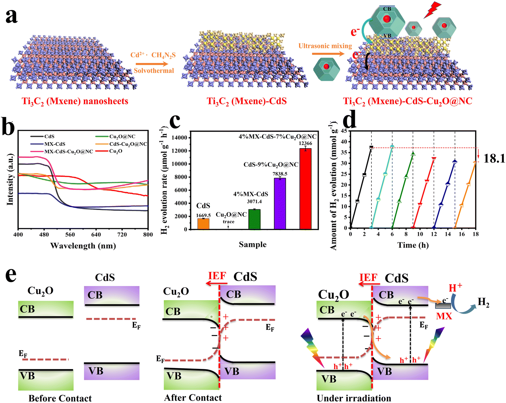 | ||
| Fig. 19 (a) Schematic diagram showing the fabrication of MX–CdS–Cu2O@NC composites; (b) UV-vis absorption spectra of different photocatalytic samples based on CdS and Cu2O; (c) hydrogen evolution of CdS, Cu2O, 4%MXCdS, CdS–9%Cu2O@NC and 4%MX–CdS–7%Cu2O@NC; (d) photocatalytic hydrogen evolution upon reuse of 4%MX–CdS–7%Cu2O@NC. Reproduced with permission.86 Copyright 2023, Elsevier. (e) Schematic illustration of interfacial electron transfer at the interface between Cu2O/CdS S-scheme heterojunctions. | ||
Rhenium disulfide (ReS2) is a direct band gap semiconductor with excellent optical properties and has also been used to develop S-scheme photocatalytic systems with Cu2O.112 Cu2O was derived from Cu foam by a thermal oxidation step followed by drop casting of previously prepared ReS2. The resulting ReS2@Cu2O S-scheme photocatalyst exhibited improved CO2 reduction activity with a CO yield of 14.3 μmol g−1 under visible light irradiation and good stability. The obtained ReS2 displayed an n-type semiconducting nature with a narrow bandgap of 1.55 eV and CB position at −0.22 V (vs. NHE). Meanwhile, Cu2O with a bandgap of 1.8 eV and VB at 1.11 V (vs. NHE) showed p-type semiconducting characteristics. This combination realized an S-scheme configuration where ReS2 and Cu2O served as the OP and RP, respectively. The established IEF and the resulting S-scheme charge transfer pathway not only promoted the separation of the photogenerated charges but also enriched electrons with high reducing abilities in the Cu2O CB, facilitating favorable CO2 reduction and CO formation. Despite the improved performance, the scarcity and high cost of Re limit its wide integration for practical applications.
6.1.1.5. Cu2O/carbon-based material S-scheme heterojunctions. Carbon-based photocatalytic and/or cocatalytic materials are among the most sustainable alternatives from the wise use of resources and economical viewpoints. With an exceptionally low bandgap, broad visible light absorption, easy functionalization, and low charge recombination, they can be developed as efficient substitutes for noble metal-based catalysts for photocatalytic applications.113–115 Graphitic carbon nitride (g-C3N4), graphene, CQDs, and amorphous carbon are the most popular materials currently applied within the catalysis-related research arena. In this section, recent research on S-scheme heterojunctions composed of Cu2O and the aforementioned carbon-based materials will be discussed.
6.1.1.5.1. Cu2O/g-C3N4 S-scheme heterojunctions. g-C3N4 as a metal-free semiconductor with visible light response, suitable band structure and abundant availability, has drawn broad attention in photocatalysis, especially for solar energy conversion and environmental remediation.116–118 Due to its remarkable features, g-C3N4 has been extensively used to date to construct S-scheme heterojunctions with organic and inorganic semiconductors.119 Regarding Cu2O, multiple studies have examined the potential of Cu2O/g-C3N4 S-scheme photocatalysts in different applications.120–123 The Zhao group fabricated a Cu2O/g-C3N4 S-scheme heterojunction as a photocatalyst for degradation of a broad range of emerging pollutants in water, including TC, hexavalent Cr salt reduction, and H2 evolution.121 Cu2O octahedra were grown on g-C3N4 sheets via the well-adopted wet chemical reduction approach (Fig. 20a). The TC degradation efficiency of the optimized Cu2O/g-C3N4 S-scheme heterojunction reached ∼100% after 120 min (Fig. 20b). The authors determined the bandgap of the as-obtained Cu2O and g-C3N4 to be 2.0 and 2.8 eV, respectively. Additionally, the VB edge of g-C3N4 and Cu2O was determined to be 1.7 eV and 1.9 eV vs. NHE, respectively. Therefore, the CB positions of g-C3N4 and Cu2O should be located at −1.1 eV and −0.1 eV vs. NHE, respectively. The free radical scavenging results showed that the dominant active species during TC degradation is the superoxide radicals ˙O2−, yet photogenerated holes h+ and hydroxyl radicals ˙OH both contribute to the overall efficiency, but to a lesser extent. Based on these analyses and taking into account that the standard redox potential of O2/˙O2− (−0.3 eV vs. NHE, the main active species for TC degradation), the photogenerated electrons on the Cu2O CB are not capable of producing ˙O2−. Therefore, the type-II charge transfer mechanism cannot be used to explain the enhanced performance of the system (Fig. 20c, left). In this vein, the S-scheme mechanism can easily rationalize the experimental results (Fig. 20c, right). Under these circumstances, Cu2O and g-C3N4 acted as the OP and RP, respectively. Photogenerated electrons at the g-C3N4 CB will be used up to accomplish H2 evolution or Cr(VI) reduction, while the resultant holes at the Cu2O VB will trigger TC degradation.121
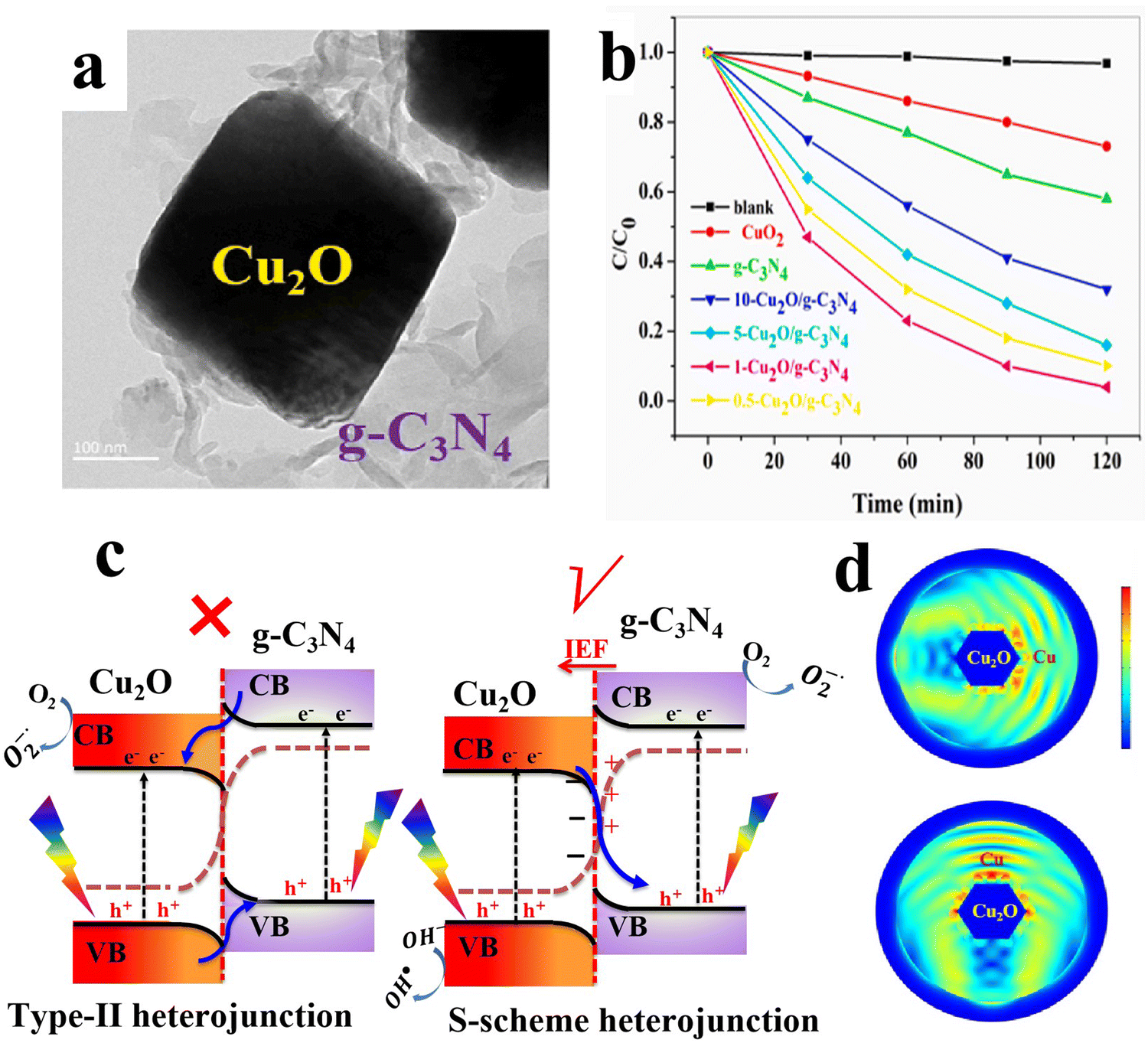 | ||
| Fig. 20 (a) TEM of Cu2O/g-C3N4; (b) photocatalytic activity of different prepared samples for TC degradation. Reproduced with permission.121 Copyright 2022, Elsevier. (c) The proposed type-II staggered band alignment (left) and S-scheme mechanism over the Cu2O/g-C3N4 heterojunction photocatalyst (right). (d) Finite-difference time-domain simulation of the two-dimension cross-section of the Cu2O@Cu structure. The light is irradiated from the side (upper) and top (lower) of the section, respectively. Reproduced with permission.120 Copyright 2022, Elsevier. | ||
When Cu plasmonic NPs were in situ generated over Cu2O octahedron by controlled chemical reduction with NaBH4, the catalytic activity was further improved.120 The obtained g-C3N4/Cu2O@Cu plasmonic S-scheme heterojunction displayed the highest CO and CH4 generation rate, which is about 13.5 and 15.5 times higher than that of pristine Cu2O, respectively. It is argued that the localized surface plasmon resonance (LSPR) of Cu NPs not only enhances light absorption by the composite but also promotes the generation and separation rate of photogenerated electron–hole pairs. Plasmonic Cu NPs can act as hotspots to maximize the intensity of the local electric field, thus enhancing the generation ability of electron–hole pairs nearby (Fig. 20d). Similar functionality attributes and plasmonic-based enhancements were reported for Au NPs anchored on the g-C3N4/Cu2O S-scheme heterojunction employed for H2 evolution and OTH degradation.90
It is worth mentioning that changing the preparation method can significantly alter the structural, optical, and electronic properties of a given semiconductor. Wei et al.,91 fabricated a g-C3N4/Cu2O–Pd S-scheme heterojunction using the well-documented in situ deposition method. However, the g-C3N4 was obtained by double calcination of a mixed melamine–urea precursor. The obtained heterostructure showed outstanding activity for H2O oxidation to H2O2 and CO2 reduction to CO. Unlike previous studies that focused on g-C3N4/Cu2O S-scheme photocatalysts, the obtained g-C3N4 had a CB position relatively lower than pristine Cu2O. Therefore, in this g-C3N4/Cu2O junction, g-C3N4 served as the OP, while Cu2O with a higher CB position functioned as the RP. This configuration synergistically promoted directional photogenerated charge separation and improved Cu2O stability, as it prevents the accumulation of holes at the Cu2O VB. After four consecutive uses, the g-C3N4/Cu2O–Pd heterojunction showed a stable photocatalytic activity, suggesting its stability and reusability. Future studies should carefully consider the stability issue of Cu2O by deliberately designing and integrating Cu2O as the RP in combination with a suitable OP, to ensure adequate protection after the transfer of photogenerated holes from the Cu2O VB during S-scheme charge separation.
6.1.1.5.2. Cu2O/CQD S-scheme heterojunctions. Due to their diverse physicochemical properties and favorable attributes, CQDs and their derived hybrids have shown promising prospects in the energy conversion and storage fields.124 Occasionally, carbon-based materials can be derived from bio-waste, thereby implementing a sustainable process while valorizing useless wastes. Derived from corn stover by a hydrothermal alkali treatment, CQDs were obtained and combined with Cu2O dodecahedrons.92 The prepared CQD/Cu2O S-scheme photocatalyst afforded enhanced TC degradation activity and outstanding stability during the cycling test. The incorporation of CQDs enhanced both the visible light absorption and the separation of electron–hole pairs. The stability of Cu2O as the OP remains debatable. In this regard, it is proposed that carbonaceous materials can provide local protection against oxidation of Cu2O,125 if photogenerated charge carriers transfer efficiently within the S-scheme heterojunction systems. However, experimental evidence is needed to support Cu2O stability, there being still significant room for exploration regarding the integration of Cu2O with C-based materials to construct efficient S-scheme photocatalysts.
6.1.1.6. Cu2O/MOF and Cu2O/MOF derivative S-scheme heterojunctions. MOFs are a class of crystalline porous materials composed of organic ligands coordinated to metal centers.126,127 Due to their extremely large surface area, high and tailored porosity, and tunable optical and electronic characteristics, MOFs are extensively studied as photo- and/or co-catalytic scaffolds.128–130 Combining MOFs with suitable semiconducting materials can result in MOF-based S-scheme heterojunctions in which the advantages of MOFs are maintained and photogenerated charge carriers undergo migration according to the S-scheme mechanism.130,131 Cu2O has been combined with various MOFs and their derivatives and tested for pollutant degradation,132,133 H2 evolution,134 CO2 reduction135,136 and organic synthesis.137
Multiple compositions with various optical and electronic properties could be attained by design. For instance, MOFs with desirable electronic features (lowest unoccupied molecular orbital (LUMO) and highest occupied molecular orbitals (HOMO)) and organic linkers with different functionalities can be combined with Cu2O to construct S-scheme heterojunctions with adequate activity, selectivity, and pronounced stability during targeted photocatalytic reactions. Moreover, MOFs can grow on different shapes of Cu2O with different exposed facets, thereby dramatically altering the optical and electronic properties.132
Controlled calcination of Cu-based MOFs can be used to prepare different heterojunctions according to the temperature and the calcination environment.134,137 For example, Cu2O@NC yolk–shell cuboctahedrons were synthesized via the calcination of Cu-BTC MOF (HKUST; btc = benzene-1,3,5-tricarboxylate) at 300 °C for 30 min under an Ar atmosphere. The prepared Cu2O@NC hollow structures showed great potential for the cross-dehydrogenative coupling (C–C bond formation) reaction of tetrahydroisoquinoline and indole. The improved activity was attributed to the prolonged lifetime of photogenerated charge carriers after separation at the interface, to multiple reflections of light by the yolk–shell hollow structure favoring light absorption, and improved stability upon heterojunction formation.137 Alternately, P-doped carbon/Cu2O heterostructures could be obtained by the calcination of triphenylphosphine-modified Cu-BTC MOFs.134
When the Cu2O structure is immersed in a solution containing BTC ligand, spontaneous in situ etching of Cu2O and coordination of Cu ions with BTC organic linkers results in the spontaneous appearance of an HKUST MOF shell, forming core–shell Cu2O@HKUST.136,138 The formation of HKUST MOF shell over the Cu2O core not only suppressed the water-induced corrosion of Cu2O during CO2 photoreduction or TC degradation reactions but also facilitated photogenerated charges separation and reactant uptake. This resulted in nanocomposites with improved activity and stability for selective photocatalytic CO2 reduction into CH4 and TC degradation.136,138
These studies highlight the diverse opportunities for designing S-scheme heterojunctions from Cu2O@MOFs and/or their derivatives. The composition, morphology, optical, and electronic properties of the targeted composites can be deliberately tuned based on the unique flexibility and vast functionalities offered by MOFs. Importantly, Cu2O@MOF core–shell or yolk–shell structures have proven profound long-term stability under operating conditions and thus can overcome the corrosion issue of Cu2O photocatalysts. Despite these merits, research studies on Cu2O@MOF S-scheme photocatalytic systems are still scarce.
6.1.1.7. Other Cu2O-based S-scheme heterojunctions. Apart from the well-known photocatalytic materials applied so far to construct heterojunctions, Cu2O can form S-scheme photocatalysts with alternative materials such as multicomponent hydroxides,139 Cu4(SO4)(OH)6140 and CsPbBr3 perovskite nanocrystals.141 Perovskite nanocrystals and layered double hydroxides (LDHs) are versatile families of inorganic materials with exceptional optoelectronic properties, customizable composition, and diverse catalytic functionalities. Owing to these merits, they have garnered significant research interest for their manipulation in photocatalytic applications.142–144 Combining the unique advantages of perovskite nanocrystals or LDH materials with tailored composition and optoelectronic features with Cu2O can result in efficient S-scheme heterojunctions with desirable activity, selectivity, and stability.
| S-scheme heterojunction | Application | Efficiency | Ref. |
|---|---|---|---|
| ZnO/CuO | MB dye degradation | ∼100% degradation in 10 min | 150 |
| ZnO/CuO | Rhodamine 6G (R6G) | ∼85% degradation in 5 h | 149 |
| ZnO/CuO | H2 evolution | The H2 evolution rate of 4655 μmol g−1 h−1 | 151 |
| ZnO/CuO | H2 evolution | The H2 evolution rate of 37.2 mmol g−1 h−1 | 152 |
| ZnO/CuO | Hg(II) reduction | 100% photoreduction within 60 min | 153 |
| CuO/In2O3 | CO2 reduction | CH4 and CO yields of 190.32 μmol g−1 h−1 and 500.46 μmol g−1 h−1, respectively | 147 |
| TiO2/CuO | Degradation of acid red 8 dye (AR8) | ∼90% degradation in 50 min | 146 |
| CeO2/CuO | Atrazine (AT) degradation | 100% degradation within 50 min | 154 |
| CuO/CdO | Levofloxacin (LVF) degradation | 96.11% degradation of LVF after 30 min | 155 |
| WO3/CuO | Cr(VI) reduction | 100% Cr(VI) reduction after 30 min | 156 |
| BiVO4/CuO | NOR degradation | 95.1% degradation of NOR after 60 min | 148 |
| CuO/ZnFe2O4 | MG degradation | 95% degradation of MG in 90 min | 157 |
| CuO/CuBi2O4 | CO2 reduction | CO and CH4 yields within 9 h of 1599.1 and 5.1 μmol m−2, respectively | 158 |
| CuO/ZnIn2S4 | CO2 reduction | CO yield = 6.9 μmol g−1 h−1 | 159 |
| CH4 yield = 54.4 μmol g−1 h−1 | |||
| CuO/Bi2S3 | CO2 reduction | CH3OH and HCOOH yields of 423.5 and 17.5 μmol g−1 h−1, respectively | 160 |
| CuO/g-C3N4 | TC degradation | 95% degradation of TC in 2 h | 161 |
| CuO/g-C3N4 | Xanthate degradation | 83.2% degradation of xanthate in 1 h | 162 |
| CuO/g-C3N4 | H2 evolution | 3848 μmol g−1 in 8 h | 163 |
| InP/CuO | CIP degradation | 81.7% degradation of CIP after 15 min | 164 |
6.1.2.1. CuO/metal oxide S-scheme heterojunctions. Different metal oxide photocatalysts have been combined so far with CuO to construct S-scheme heterojunctions including Cu2O,165,166 TiO2,146 ZnO,149–153,167 WO3,156 CdO,155 NiO,168 In2O3,147 ZrO2169 and CeO2.154 In this regard, CuO-based S-scheme heterojunctions with metal oxides were fabricated based on different approaches including the sol–gel technique followed by calcination in air,153,154,169 MOFs-derived method,147,150 and solid-state mixing.146 Of them, the MOF-based approach shows particular promise as the obtained photocatalysts may partially retain the precursor porosity, inheriting them with abundant active sites, higher light absorption, minimized charge carrier recombination, and feasible mass and/or charge transfer.150
In this vein, a CuO/ZnO S-scheme heterojunction was directly formed by calcination of Cu-rich ZIF-8. HRTEM and XRD results confirmed the formation of the CuO phase alongside the wurtzite phase ZnO. The nanocomposite with optimum CuO loading exhibited fast degradation kinetics for different targeted pollutants including MB and RhB dyes, bisphenol A (BPA), and TC in the presence of peroxymonosulfate (PMS).150 The excellent activity was primarily attributed to the enhanced visible light absorption and the synergistic role of Cu and Zn species for PMS adsorption and activation. After light illumination, photogenerated electrons and holes at the CuO CB and ZnO VB, respectively, were maintained to trigger the redox generation of active species. Cu2+/Cu+ pairs play a key role as ionizable cocatalysts during free radical formation.
In a recent study, a MOF-on-MOF interfacial engineering strategy was adopted to fabricate an In2O3 nanosheet-wrapped CuO core–shell structure (CuO@In2O3) S-scheme heterojunction for efficient photocatalytic CO2 reduction (Fig. 21).147 Cu-HKUST MOFs with octahedral morphology were first fabricated. Then, In-MOF nanosheets were grown at the outer surfaces of Cu-MOF octahedrons (Fig. 21a and b). Upon calcination in an air atmosphere, the MOF-on-MOF structure transformed into a CuO@In2O3 core–shell composite with an almost identical shape to the original precursor (Fig. 21b). The CuO@In2O3 heterostructure was proven to have excellent CO2 reduction activity ca. CH4 and CO yields of 190.32 μmol g−1 h−1 and 500.46 μmol g−1 h−1, almost 2.1 and 10.3 times and 2.4 and 7.9 times higher than that of pristine CuO and In2O3, respectively (Fig. 21c). The bandgap and VB position values of CuO and In2O3 were calculated to be 1.98 and 2.86 eV, and 1.62 and 1.22 eV, respectively. Based on this analysis, the authors proposed the charge separation mechanism as displayed in Fig. 21d. In2O3 is an n-type semiconductor with a Fermi level and CB position higher than those of the p-type CuO. Therefore, CuO and In2O3 functioned as the OP and RP in this configuration. Under light irradiation, electrons with lesser reduction potential at the CuO CB recombine with holes of lower oxidation potential at the In2O3 VB, while photogenerated electrons and holes with the highest reduction and oxidation power are maintained preferentially at the In2O3 CB and CuO VB, respectively.
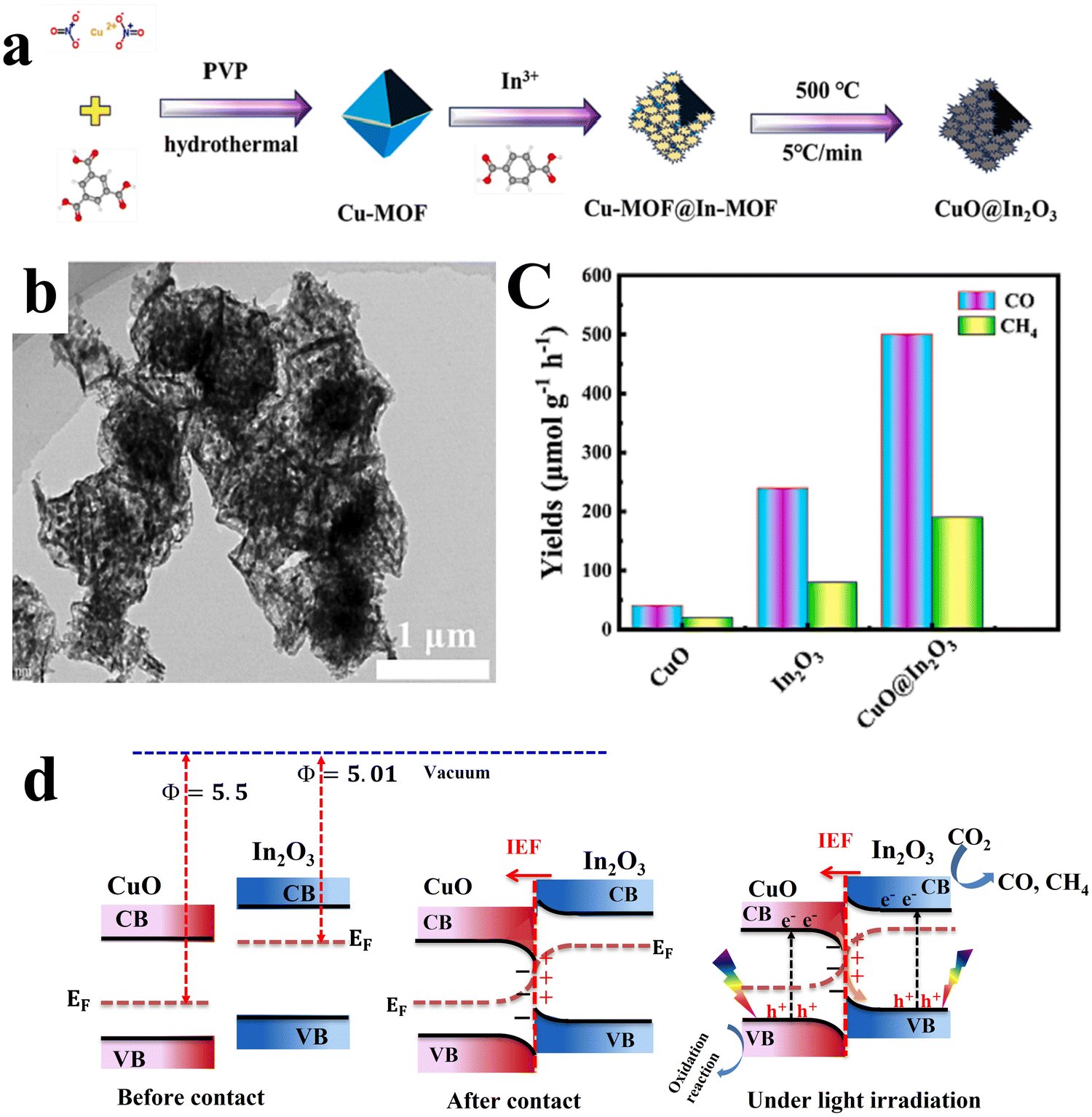 | ||
| Fig. 21 (a) Schematic of the synthesis of CuO@In2O3 composites; (b) TEM images of CuO@In2O3 composites; (c) production rates of CO and CH4 production over the studied photocatalysts. Reproduced with permission.147 Copyright 2023, Elsevier. (d) Schematic layout of the band structure of the CuO/In2O3 S-scheme heterojunction and proposed charge transfer dynamics and reaction mechanism. | ||
This S-scheme charge transfer mechanism, along with the enhanced light absorption, improved CO2 adsorption, and the large density of exposed active sites of the nanocomposites compared to the pristine components, were all responsible for the activity enhancement. These studies exemplify the effectiveness of the MOF-based strategy for customizable CuO-based S-scheme heterojunctions with desirable features and excellent performance.
As mentioned before, conductive materials, metallic species, and other co-catalytic scaffolds are widely integrated within S-scheme heterojunctions to boost the charge transfer process and enhance the overall activity. For example, when plasmonic Ag NPs are deposited over the ZnO/CuO system using DC magnetron sputtering, the photocatalytic degradation activity for rhodamine 6G (R6G) was drastically enhanced.149 CuO and ZnO are typical p- and n-type semiconductors, respectively, with staggered band positions that can form an S-scheme configuration with ZnO as the OP and CuO as the RP. Hot electrons are generated within Ag NPs due to LSPR excitation. Under these conditions, a double built-in electric field was established at the Ag–ZnO and ZnO–CuO interfaces. The double field prevents the recombination of electrons from Ag and the CuO CB with the holes in the VB of ZnO that are proposed to be responsible for the observed photocatalytic activity. Thus, full use of photogenerated electrons at Ag and CuO became possible, favoring improved activity. Similarly, Au NPs can also be used to enhance the visible light absorption of the CuO–ZnO S-scheme hybrid due to its LSPR band at about 560 nm.151
The integration of an S-scheme heterojunction with plasmonic metal NPs is a valid approach to satisfactorily promote the overall performance of the system. Notably, non-noble plasmonic metals are promising alternatives due to their earth abundance, tunable features, and feasible manipulation of their LSPR response beyond the visible range.50,170
In addition to metallic species, non-metallic entities offer substantial potential for catalytic applications. In this regard and due to the excellent electrical conductivity of graphene, it is extensively employed as a support/cocatalyst in photocatalytic and electrocatalytic applications.171 When ZnO and CuO were anchored on graphene, the system displayed the highest H2 production rate of 37.2 mmol g−1 h−1, which was 3.3 times higher than pristine CuO/ZnO alone.152 In this configuration, graphene further boosted the S-scheme charge transfer owing to its unique electrical conductivity favoring the transport of photoexcited electrons between the semiconductors.
Other carbon-based scaffolds such as carbon nanotubes (CNTs) and CQDs can exhibit similar functions. Recently, graphdiyne (GDY), a rising star of 2D carbon allotropes, has demonstrated excellent charge carrier transfer efficiency and high conductivity.172 These features make GDY a leading candidate in photo- and electro-catalytic applications.173,174 Future studies are encouraged to elaborate on the role of GDY as a cocatalyst in combination with Cu-based S-scheme photocatalytic systems. Carbon-based materials can be used as active cocatalysts to boost the S-scheme charge migration and separation, improving activity and/or modifying the selectivity of the photocatalytic reaction.
The studies discussed in this section provide a clear picture of CuO/metal oxide-based S-scheme photocatalysts. CuO-based S-scheme systems with metal oxide semiconductors showed improved activity and better stability over their Cu2O-based counterparts.146,154 In conclusion, CuO can serve as the RP or OP in S-scheme systems due to its suitable band positions and good stability. Partial reduction of Cu(II) to Cu(I) during the photocatalytic process can enhance the efficiency as the redox pair can act as an ionizable cocatalyst. Careful consideration is needed during bandgap measurements, Fermi level analysis, and band position determination to allow appropriate justification of the S-scheme heterojunction configuration.
6.1.2.2. CuO/binary metal oxide S-scheme heterojunctions. CuO has considerable potential in pollutant degradation through Fenton-like and PMS-based advanced oxidation processes. In this vein, Cu2+/Cu+ redox pairs act as active sites for the activation and generation of reactive species by swinging between the two redox states while transferring one electron to H2O2 or PMS.175,176 The initial Cu2+ can be restored during the reaction course by the photogenerated hole to sustain the activity of the photocatalyst. It is found that the Cu+/Cu2+ redox pair acts as an activator in Fenton-like pollutant degradation processes. Its role has also been proposed in other redox reactions such as CO2 reduction and H2O2 generation.
Since CuO activity is limited by the recombination rate of photogenerated electron–hole pairs, it is highly desirable to integrate CuO in S-scheme systems to mitigate the limitation derived from this favorable charge recombination and promote the photocatalytic degradation activity of the system.148,157 Bismuth vanadate (BiVO4) is an example of a binary metal oxide with high oxidation potential, thus acting as the OP in S-scheme photocatalytic systems. With the potential to tailor the exposed facets, surface homojunction formation between {010} and {110} planes of BiVO4 is possible. Typically, when BiVO4 is excited with suitable light, electrons are transferred to the {010} facets and holes are accumulated on the {110} facets.177,178 In this regard, when CuO is deposited over the {010} facets of BiVO4, an S-scheme heterojunction is established at the interface (Fig. 22a, b and e), both BiVO4 facets drive electrons to CuO, thereby accelerating the Cu2+/Cu+ cycle and enabling efficient PMS activation, all of which contribute to system activity, stability, and durability (Fig. 22c and d).148 Photogenerated holes that accumulated at the {110} facets would be consumed for PMS activation as well (Fig. 22e). Inspired by this synergism of charge separation, the CuO/BiVO4 S-scheme photocatalysts exhibited excellent norfloxacin (NOR) degradation efficiency of 95.1% within 60 min in the presence of PMS (Fig. 22c), which was 3.65 and 2.45 times that of CuO and BiVO4, and pronounced stability over four recycling cycles (Fig. 22d).
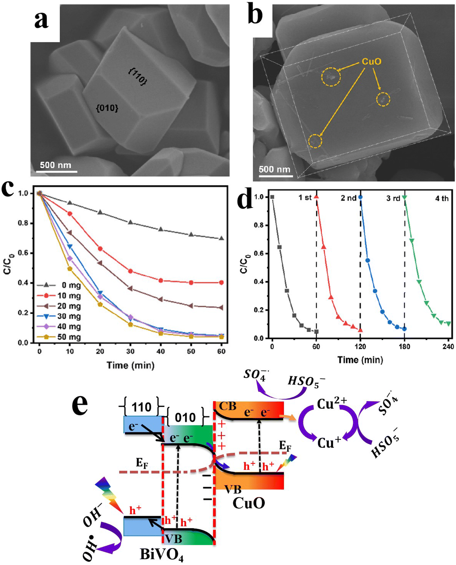 | ||
| Fig. 22 FESEM images of (a) BiVO4 and (b) CuO/BiVO4 samples, highlighting the location of CuO NPs. (c) Photocatalytic degradation efficiency of CuO/BiVO4 for the NOR solution at different PMS doses and (d) the recyclability of the CuO/BiVO4 photocatalyst. Reproduced with permission.148 Copyright 2024, Elsevier. (e) Proposed mechanism of NOR degradation over the CuO/BiVO4/PMS system. | ||
ZnFe2O4 and CuBi2O4 are among the binary metal oxides that have been reported forming S-scheme photocatalytic systems with CuO.157,158 Of these, ZnFe2O4 and CuO were uniformly immobilized on the surface of 2D BiOBr nanoplates to build a dual S-scheme configuration, which not only steered the charge migration to desirable positions, but also endowed the system with ultimate robustness.157 Significantly, the ternary S-scheme heterojunctions attained optimum photocatalytic malachite green (MG) degradation efficiency of 95% in 90 min and ca. 6.57, 3.78, and 4.31 times faster reaction kinetics compared to BiOBr, ZnFe2O4, and CuO, respectively. Despite the potential of the resultant S-scheme photocatalysts after the combination of binary metal oxides with CuO, the number of studies in this area remains limited.
6.1.2.3. CuO/metal sulfide S-scheme heterojunctions. Metal sulfides (MS) have attracted attention as suitable semiconductors to form S-scheme heterojunctions with CuO due to their excellent visible light absorption capability and high reduction potential.179–181 After being integrated into an S-scheme system, the activity and selectivity of the resulting CuO heterojunctions were optimized, and the stability issue of MS was effectively addressed. MS functions as a RP when integrated with CuO in an S-scheme configuration, thus photogenerated holes on their VBs are recombined with photogenerated electrons from CuO under the influence of IEF. In light of these peculiar enhancements, the CuO@ZnIn2S4 heterojunction was constructed by a hydrothermal method and applied for CO2 photoreduction.159 Ag NPs were introduced onto CuO@ZnIn2S4 by photodeposition. The heterostructure components interact strongly, and an interfacial Cu–S bond was formed at the interface, as evidenced by the XPS results of the S 2p spectrum (Fig. 23a). Upon this strong interaction and the formation of a new charge transfer channel, i.e., Cu–S bonds, the charges were redistributed at the interface, and electrons moved from ZnIn2S4 to CuO. This charge transfer induced a partial reduction of Cu(II) in CuO to Cu(I) after combination with ZnIn2S4 (Fig. 23b). The reduction extent further increased after the deposition of plasmonic Ag NPs, as Ag possesses a higher Fermi energy level, and electrons can flow from Ag to CuO to form a metal/semiconductor junction. The charge distribution and transfer at the interface were further confirmed through charge density difference calculations using DFT theoretical simulations (Fig. 23c). After combining ZnIn2S4 and CuO, regions of charge depletion and accumulation were formed at ZnIn2S4 and CuO, respectively, indicating electron transfer from ZnIn2S4 to CuO (Fig. 23d). Under light irradiation, the charge transfer direction reversed and photogenerated electrons at the CuO CB moved to recombine with holes on the ZnIn2S4 VB. Meanwhile, electrons and holes with the highest redox potential at ZnIn2S4 and CuO, respectively, are maintained to initiate CO2 reduction and oxidation reactions (Fig. 23e). The remarkable catalytic activity and selectivity observed for CO2 reduction were assigned to three factors: (i) the S-scheme charge transfer mechanism operating for CuO@ZnIn2S4, driving the charge separation at the interface, (ii) the emergence of Cu–S covalent bonds that open an additional channel for accelerated charge carrier migration, and (iii) Ag NPs exploited its LSPR effect and enhanced the product selectivity by controlling the reaction intermediate.159
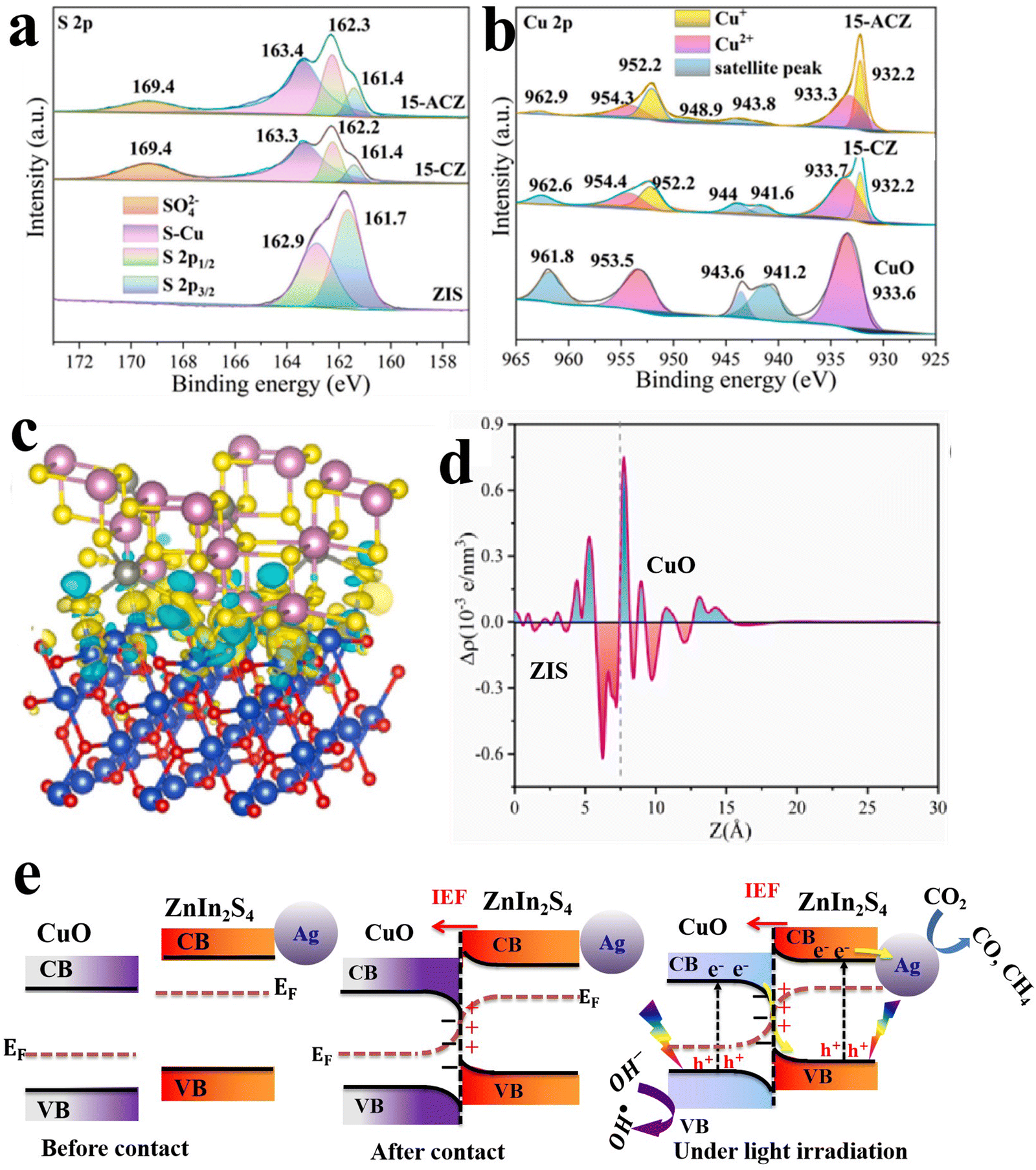 | ||
| Fig. 23 High-resolution XPS core levels of (a) S 2p and (b) Cu 2p; the simulated charge density difference (c) and planar average charge difference density (d) over the ZIS/CuO composite. Reproduced with permission.159 Copyright 2023, Elsevier. (e) Charge transfer mechanism and CO2 reduction over the Ag/CuO@ZnIn2S4 S-scheme photocatalytic system. | ||
In other example, reduced graphene oxide (r-GO) was used as a cocatalyst of the CuO/Bi2S3 S-scheme photocatalyst. The synthesized nanocomposite exhibited the maximum CO2 reduction activity with a methanol yield of 423.52 μmol g−1 h−1 and the selectivity approached 99%.160 These studies provide a useful approach to constructing S-scheme heterojunction systems based on CuO/MS in combination with effective cocatalysts for tuning product selectivity, promoting catalytic activity, and enhancing the stability of the system. CdS, stoichiometric ZnCdS, and other MS are plausible alternatives for future studies.
6.1.2.4. CuO/g-C3N4 S-scheme heterojunction. CuO in combination with g-C3N4 can form an S-scheme heterojunction in which CuO and g-C3N4 will function as the OP and RP, respectively. In a recent study, Wang and her group developed a fascinating strategy to extract Cu ions from solid wastes using an acid-leaching approach.161 After being extracted, Cu ions were mixed with a definite amount of melamine and cyanuric acid as g-C3N4 precursors, and the final macromolecular polymer was subjected to calcination in air at 550 °C to yield CuO/g-C3N4 nanocomposites. When tested for TC photocatalytic degradation, the CuO/C3N4 S-scheme heterojunction exhibited 95% degradation efficiency after 2 h with ca. 45% mineralization. After the S-scheme charge transfer mechanism came into action, photogenerated electrons and holes with the strongest reduction and oxidation potentials were preserved at C3N4 and CuO, respectively, retaining the outstanding redox ability of the CuO/C3N4 nanocomposite for the effective generation of active species.161
The photocatalytic efficacy of the CuO/g-C3N4 S-scheme nanocomposite obtained via hydrothermal growth of CuO over g-C3N4 was also tested for degradation of xanthate.162 Compared with pure g-C3N4, the photocatalytic degradation performance of the composite photocatalyst improved by a factor of 5.2. Thurga et al.,163 tested the H2 evolution activity of the CuO/g-C3N4 system during formaldehyde photoreforming. The authors measured the bandgap energies of CuO and exfoliated g–C3N4 to be 1.85 and 2.85 eV, respectively. The CB and VB positions were calculated to be −0.98 and −0.77 eV for g–C3N4, and +1.87 eV and +1.08 eV for CuO, respectively. The Mott–Schottky (M–S) analysis revealed n- and p-type semiconducting characteristics of g-C3N4 and CuO, respectively. Based on these results, the photocatalytic mechanism and charge transfer process were proposed. Upon contact, electrons will move from exfoliated g-C3N4 toward CuO due to Fermi level differences until equilibrium is achieved. Consequently, an IEF at the interface could promote the migration of charge carriers and limit their recombination. Upon light irradiation, the S-scheme mechanism governs the charge transfer such that photogenerated holes and electrons are maintained at the CB and VB of g-C3N4 and CuO, triggering H2 reduction and formaldehyde oxidation, respectively. This charge carrier separation granted the nanocomposite with improved H2 evolution activity ca. 7 and 13 times higher than that of exfoliated g-C3N4 and CuO, respectively.
In these studies, the nanocomposite showed good cycling stability, manifesting the robustness of CuO/g-C3N4 S-scheme heterojunctions during photocatalytic applications. Other carbon-based materials in combination with CuO to construct S-scheme photocatalytic systems have not yet been reported.
6.1.2.5. Other CuO-based S-scheme heterojunctions. Many innovative S-scheme heterojunctions based on CuO can be constructed by leveraging its adequate band positions. Metal chalcogenides, bismuth oxyhalides, polymers, MOFs, and covalent organic frameworks (COFs) are among the various photocatalytic scaffolds that can be integrated with CuO to form prospective S-scheme heterojunctions. An attempt was made by Parsaei, Rashid, and coworkers to deliberately construct InP/CuO–C cubic heterostructures derived from an In/Cu bimetallic MOF followed by calcination and phosphitization steps (Fig. 24a).164 The InP/CuO nanocomposite retained the cubic morphology of pristine In/Cu-MOFs, yet with pronounced porosity (Fig. 24b and c). The photocatalytic activity of the obtained catalyst was investigated for degradation of ciprofloxacin (CIP) antibiotic in a microfluidic photoreactor (Fig. 24a). Different parameters affecting the catalyst performance such as catalyst dose and CIP concentration were studied. The CIP photodegradation efficiency increased from 48.0 to 64.9% as the amount of InP/CuO–C rose from 1.0 to 2.0 mg. However, further increasing the catalyst loading to 3.0 mg resulted in a decline in the photodegradation efficiency to 52.4% (Fig. 24d). In contrast, the photodegradation efficiency gradually decreased with increasing CIP concentration due to the blocking of the catalyst confined active sites after the adsorption of CIP from the solution thus preventing the adsorption of more CIP molecules (Fig. 24e).
 | ||
| Fig. 24 (a) Schematic illustration of InP/CuO–C fabrication from the In/Cu-MOF precursor and CIP photodegradation in a spiral microfluidic photoreactor; FESEM (b) and TEM (c) images of the InP/CuO–C sample. Photodegradation efficiency of CIP over InP/CuO–C at different InP/CuO–C dosages (d), and different CIP concentrations (e). Reproduced with permission.164 Copyright 2023, Elsevier. | ||
Regarding the charge transfer pathway and reaction mechanism, the work functions of CuO and InP were found to be 5.5 and 4.6 eV, respectively, implying charge transfer from InP into CuO after contact to equilibrate Fermi levels between them and confirming the formation of an IEF. Upon exposure to light, electrons in the CuO CB will recombine with holes in the InP VB. This scenario lays the foundation for a possible S-scheme charge transfer pathway. Meanwhile, photogenerated charge carriers with stronger redox capacities were retained to trigger the formation of reactive species or used directly to activate CIP degradation.
| S-scheme heterojunction | Application | Efficiency | Ref. |
|---|---|---|---|
| TiO2 spindle/CBO | TC degradation | Degradation of 82% in 60 min | 190 |
| Fe2O3/CBO | 4-NP and RhB degradation | Degradation of 90.6 and 95.8% for 4-NP and RhB after 50 and 40 min, respectively | 191 |
| CeO2−x/CBO | Toluene degradation | Degradation of 100% in 120 min | 192 |
| WO3/CBO | TC degradation | Degradation of 70% in 120 min | 193 |
| Bi2S3/CBO | MB and MO degradation | Degradation of 98.8 and 99.2% for MB and MO after 80 min, respectively | 194 |
| BiOBr/CBO | TC degradation | Degradation of 90.3% in 35 min | 176 |
| BiOCl/CBO | Diclofenac (DCF) degradation | Degradation of 90% in 60 min | 195 |
| Bi4O5I2/CBO | E. coli and S. aureus deactivation | Inactivation of 100% E. coli in 20 min and S. aureus in 40 min | 196 |
| (BiO)2CO3/CBO | RhB and MO degradation | Degradation of 97.8 and 98.3% of RhB and MO within 70 min | 197 |
| WO3/CBO | CO2 reduction | CO and CH4 yields of 980.4 and 63.7 μmol m−2, respectively, after 7 h | 198 |
| Na-P25/CBO | H2 generation | H2 yield of 2695.7 μmol g−1 h−1 | 196 |
| MnO2/CFO | MB degradation | Degradation of 92.5% in 240 min | 199 |
| ZnIn2S4/CFO | CIP degradation | Degradation of ∼100% in 60 min | 200 |
| CWO/Bi12O17Cl2 | TC degradation | Degradation of 94.7% in 30 min | 188 |
6.1.3.1. CuBi2O4. Dibismuth copper oxide (CuBi2O4, CBO) is a p-type semiconductor with a narrow bandgap (1.5–1.8 eV), thus exhibiting light absorptivity in the whole visible region. It possesses a sufficiently negative CB to trigger most photocatalytic reduction reactions of current interest. The spinel structure of CBO renders it with exceptional stability thus avoiding photo-corrosion occurring in single Cu or Bi oxides.191,192,195,201 Owing to these ample features, CBO has been widely integrated into S-scheme photocatalysts in combination with metal oxides,190–193,197,198,201–208 bismuth oxyhalides,176,195,196 and metal sulfides.194 Most of these studies employed the one-step approach to prepare CBO, in which Bi3+ and Cu2+ are allowed to react with a suitable base (usually NaOH) under hydrothermal conditions. The obtained 1D CBO microrods can be introduced as a substrate during the solvothermal growth of another component. Alternatively, it can be fed into the spraying mixture to be loaded over the target fiber or semiconductor thin film.193
Generally, CBO-based S-scheme heterojunction photocatalysts have been used for environmental remediation applications including organic pollutant degradation, bacteria inactivation, and Cr(VI) reduction. In these systems, CBO functions as a potent RP, where photogenerated electrons with the highest reduction potential reside in its highly negative CB. For example, the degradation efficiency of the Fe2O3/CBO S-scheme heterojunction photocatalyst for 4-nitrophenol (4-NP) and RhB reached 90.6% and 95.8% after 50 and 40 min, respectively, of visible light irradiation.191 Interestingly, a mixed solution of 4-NP and RhB pollutants was mostly decomposed after 120 min of natural sunlight irradiation. The ESR and XPS results manifested that an S-scheme charge transfer mechanism was implemented at the interface in such a way that electrons with the highest reduction potential accumulate in the CBO CB to activate O2 reduction into ˙O2−. Meanwhile, photogenerated holes at the Fe2O3 VB were either used directly for pollutant degradation or to oxidize hydroxide ions into hydroxyl radicals. Photogenerated holes, ˙O2− and ˙OH, were found to be the main reactive species responsible for the degradation of 4-NP and RhB.
Borjigin et al.192 fabricated an oxygen vacancy (OV)-rich CeO2/CBO S-scheme system for photocatalytic oxidation of gaseous toluene. CeO2−x nanoplates were grown over CBO nanorods using a solvothermal approach. High-resolution TEM images showed the CeO2−x surface with numerous distinct lattice disorders (OV). The existence of OV was also confirmed via a distinctive EPR signal at g = 2.003 (Fig. 25a). Noteworthy, the OV-signal in the composite sample persists even after five reuses, indicating the excellent stability of OV in the composite material, which contributed to sustaining the activity of the prepared catalyst. To investigate the strong electronic interaction between CBO and CeO2−x in the composite sample, the authors performed DFT simulations.
 | ||
| Fig. 25 (a) EPR spectra of pure CeO2−x, CBO, and fresh and used CeO2/CBO with optimal CBO loading (CC15) sample; (b) the electron density differences transection map and planar-averaged electron density difference, Δρ along the Z-axis for CeO2−x/CBO, where the red and blue regions correspond to the electron depletion and enrichment region, respectively. Toluene degradation (c) and CO2 yield (d) as a function of irradiation time over the as-prepared catalysts. Reproduced with permission.192 Copyright 2024, Elsevier. | ||
The results depict the electron density difference at the interface where electron depletion (negative values of Δρ) and enrichment (positive values of Δρ) regions appear at the CBO and CeO2−x sides, respectively, indicating electron transfer from CBO to CeO2−x across the heterojunction interface (Fig. 25b). Such electron transfer after compositing is responsible for the formation of an IEF, thus driving S-scheme electron transfer under light irradiation. Supported by the OV and the S-scheme mechanism, the optimum CBO/CeO2−x composite showed upgraded toluene degradation of 100% after 120 min together with TOC removal of ∼90% (Fig. 25c and d). Interestingly, the CBO/CeO2−x catalyst retained its excellent degradation activity even after 32 recycling tests.
In another study, the Cu2+/Cu+ redox cycle was found to effectively sustain the PMS activation of the CBO/BiOBr S-scheme photocatalyst during TC degradation in a Fenton-like process.176 Compared with bare CBO and BiOBr, the CBO/BiOBr S-scheme photocatalyst degraded 90.3% of TC within 35 min, with the reaction rate increased by 8.4 and 3.3 times, respectively. The S-scheme-induced accumulated electrons at the CBO CB can efficiently sustain the Cu2+/Cu+ redox cycle, thus maintaining the activity of the CBO/BiOBr nanocomposite. These studies ultimately illustrate the effectiveness of CBO-based S-scheme heterojunctions for environmental remediation. Besides the S-scheme heterojunction enhancing the charge separation and maintaining the highest redox potential during the degradation process, additional contributors can introduce more functionalities and improve the activity and stability of the system. Loading cocatalysts, defect engineering, and incorporating redox pairs are promising strategies to achieve these goals.194
Apart from pollutant degradation, CBO-based S-scheme photocatalytic systems have also been tested for other energy-related applications such as H2 evolution202 and CO2 reduction.198,203 For instance, Shi et al.198 showed that the CO2 reduction activity is strongly correlated to the heterojunction formation between WO3 and CBO. Bare WO3 and CBO exhibited almost no valuable product upon visible light illumination. However, CO and CH4 were detected as major products after the construction of the WO3/CBO S-scheme junction, and the product yield increased gradually with CBO content. The optimal yields of CO and CH4 after 7 h irradiation were 980.4 and 63.7 μmol m−2, respectively, attained for WO3/CBO-4 (4 is the number of spraying cycles for introducing CBO). The authors confirmed the establishment of an S-scheme charge transfer mechanism through different data, such as time-resolved photoluminescence (TRPL), ISIXPS, and catalytic activity measurements under various light conditions.
In these studies, it was argued that the accumulated electrons in the CBO CB, after being separated following an S-scheme trend, are used to accomplish CO2 reduction or H2 evolution. Meanwhile, holes in the VB of the OP were consumed for oxidation reactions. In general, CBO is an outstanding RP alternative. Its S-scheme materials exhibited superior activity in various photocatalytic applications with notable stability.
6.1.3.2. CuFe2O4. Copper ferrite (CuFe2O4, CFO) with a spinel structure and p-type semiconducting nature possesses excellent visible absorption and carrier mobility. These merits render CFO double functionality in S-scheme heterojunctions as a reducing photocatalyst and Fenton activating agent during pollutant degradation. In particular, the CFO role in environmental remediation includes activating the Fe3+/Fe2+ and Cu2+/Cu+ redox pairs, which can enhance the generation of free radicals and active species responsible for the catalytic activity of the system. In this context, CFO was coupled with MnO2 and ZnIn2S4 to construct S-scheme heterojunctions for MB degradation and a self-Fenton system for CIP mineralization, respectively.199,200 The construction of a S-scheme heterojunction between CFO and ZnIn2S4 was supported through different means including ISIXPS, ESR, activity measurements, and DFT simulations.200 All methods confirmed charge transfer from CFO to ZnIn2S4 after contact. The authors measured the generated H2O2 in the system and found that CFO/ZnIn2S4 (1
:5) (1:5, representing the weight ratio of CFO to ZnIn2S4) afforded the maximum yield of 2545.4 μmol g−1 h−1, which was 3.9 and 19.3 times higher compared to CFO and ZnIn2S4. The in situ generated H2O2 was effectively used to produce reactive species efficient for the degradation of numerous organic pollutants, including CIP, sulfamethoxazole, and amoxicillin, with excellent activity and stability. Notably, Fe2+ and Cu+ in CFO/ZnIn2S4 were the main active sites to activate H2O2 to generate ˙OH. The photogenerated electrons accumulated in the CB of CFO, following the S-scheme charge separation pathway, could reduce Fe3+ and Cu2+ to maintain the cycling of Fe3+/Fe2+ and Cu2+/Cu+ pairs. This sustained the continuous generation of active Fe2+ and Cu+ species for further CIP degradation. This study provides comprehensive insights into the integration and manipulation of CFO-based S-scheme heterojunction photocatalysts. Despite the promising potential of CFO as an RP, its integration into S-scheme systems remains limited.
6.1.3.3. CuWO4. Copper tungstate (CuWO4, CWO) is a promising n-type semiconductor with a narrow bandgap of ∼2.2–2.4 eV, highly positive VB position and adequate chemical stability.182,188 Therefore, CWO is widely employed as an OP. Except for integration with Bi12O17Cl2 to construct an S-scheme system for TC degradation, no research studies have been conducted to explore the potential of CWO in the corresponding S-scheme systems. A CWO/Bi12O17Cl2 S-scheme heterojunction with rich OV was obtained using a simple precipitation method.188 CWO NPs were attached to Bi12O17Cl2 NSs with strong interaction between CWO and Bi12O17Cl2 as revealed from HRTEM images and XPS data. Due to the contribution of several factors, including enhanced light absorption, reduced electron–hole recombination, and longer photogenerated electron lifetime, the optimal CWO/Bi12O17Cl2 exhibited the highest activity. In the S-scheme configuration, the photogenerated electrons and holes were retained in the CB of Bi12O17Cl2 and the VB of CWO, respectively, contributing effectively to the production of reactive species.
6.2. Cu-based chalcogenides
Copper-based chalcogenide materials are chemical compounds composed of Cu (whether solely or encompassing additional transition metal, main-group metal or semi-metal ions) are bonded to one or more chalcogenide elements (S, Se, or Te). Cu chalcogenides are a versatile class of interesting materials with structural and compositional flexibility, several types of crystal structures, semiconducting nature with often a p-type entity and prominent optical features including small bandgap, high absorption coefficient and highly negative CB position, thus fitting well as the RP in S-scheme heterojunctions.209–213 The family includes copper sulfides (CuxS, (1 ≤ x ≤ 2)), copper-based binary sulfides (e.g.: CuInS2, Cu2WS4, Cu2MoS4, Cu3SnS4), and copper selenides (CuSe). This section will provide a detailed overview of copper-based chalcogenide photocatalytic materials, particularly sulfides and selenides, their optical and electronic properties, and possible integration in S-scheme heterojunctions. Table 6 summarizes S-scheme heterojunctions based on Cu-containing chalcogenides for different photocatalytic applications.| S-scheme heterojunction | Application | Efficiency | Ref. |
|---|---|---|---|
| Ga2S3/CuS | CO2 reduction | CH4 yield of 18.8 μmol g−1 h−1 | 214 |
| CuS/ZnIn2S4 | H2 generation | H2 yield of 4653.43 μmol h−1 g−1 | 215 |
| CuS/ZnIn2S4 | CO2 reduction | CH4 and CO yields of 4.8 and 55.3 μmol g−1 h−1, respectively | 216 |
| CuS/SnIn4S8 | H2 generation | H2 yield of 6235.72 μmol g−1 h−1 | 217 |
| CuS/CdZnS | H2 generation | H2 yield of 5904 μmol g−1 h−1 | 218 |
| CuS/Mn0.5Cd0.5S | H2 generation | H2 yield of 40.6 mmol h−1 g−1 | 219 |
| CuS/Mn0.3Cd0.7S | H2 generation | H2 yield of 42.43 mmol g−1 h−1 | 220 |
| CuS/ZnCoS2 | H2 generation | H2 yield of 6167 μmol g−1 within 3 h | 221 |
| CuS/Bi5O7I | E. coli disinfection | Complete inactivation in 180 min | 222 |
| CuS/Cu-BDC MOF | H2 generation | H2 yield of 9343 μmol g−1 h−1 | 223 |
| CuS/g-C3N4 | TC degradation | Degradation of 95% after 40 min | 224 |
| WO3/CuInS2 | TCH degradation | Complete degradation in 6 h | 225 |
| SnNb2O6/CuInS2 | Cr(VI) reduction | Degradation of 97.6% after 90 min | 226 |
| UiO-66 MOF/CuInS2 | N2 fixation and O2 reduction | NH3 and H2O2 yields of 398 and 4073 μmol g−1 h−1, respectively | 51 |
| Zn0.5Cd0.5S/CuInS2 | H2 generation | H2 yield of 7.73 mmol g−1 h−1 | 227 |
| ZnIn2S4/CuInS2 | TC degradation and Cr(VI) reduction | Degradation of 90.1 and 98.7% for TC (120 min) and Cr(VI) (60 min) | 228 |
| g-C3N4/CuInS2 | O2 reduction | H2O2 yield of 1247.6 μmol g−1 h−1 | 229 |
| Cu2WS4/CdS | H2 generation | H2 yield of 6017 μmol g−1 h−1 | 230 |
| MoS2/Cu2WS4 | BP-1 degradation and Cr(VI) reduction | Degradation of 89.1 and 98.7% for Cr(VI) and BP-1, respectively, in 90 min | 231 |
| Cu2MoS4/Cd0.9In0.1Se | H2 generation | H2 yield of 6358.42 μmol g−1 h−1 | 232 |
| BiOBr/Cu3SnS4 | CIP degradation | Degradation of 93% after 180 min | 233 |
| CuSe/PANI | MB degradation | Degradation of 100% after 45 min | 234 |
| TiO2/Cu3P | H2 generation | H2 yield of 5.83 mmol g−1 h−1 | 235 |
| BiOCl/Cu3P | TC degradation | Degradation of 86% after 6 min | 236 |
| ZnWO4/Cu-MOF | TC degradation | Degradation of 98% after 60 min | 45 |
| In-MOF@Cu-MOF | Cr(VI) reduction | Reduction of 98% after 60 min | 237 |
| Cu-MOF/CuInS2 | H2 generation | H2 yield of 1013.35 μmol g−1 h−1 | 238 |
| Cu-MOF/Mn0.05Cd0.95S | H2 generation | H2 yield of 547.5 μmol after 5 h | 239 |
| Cu-MOF/Cd0.5Zn0.5S | H2 generation | H2 yield of 18986 μmol g−1 h−1 |
240 |
| CeO2/Cu-TCPP MOF | CO2 reduction | CO and CH4 yield of 57.41 and 3.46 μmol g−1 h−1, respectively | 241 |
| Cu-MOF/COF | H2 generation | H2 yield of 15.3 mmol g−1 h−1 | 242 |
To ameliorate the performance of pristine CuS during CO2 photoreduction, improve CO2 adsorption and activation, and enhance the product selectivity, Ga2S3 (GS) was coupled to CuS to build an S-scheme heterojunction using a two-step hydrothermal synthesis.214 The 30-GS/CuS (with 30% wt of GS) S-scheme photocatalyst afforded after 4 hours irradiation of CH4 yielded 75.2 μmol g−1, markedly surpassing that of GS (3.4 μmol g−1) and CuS (3.7 μmol g−1). In addition, the GS/CuS S-scheme photocatalyst showed no notable decline in activity after five consecutive cycles to check the catalytic stability. Based on bandgap and band energy levels, KPFM measurements, and DFT calculations, the authors were able to assign GS and CuS as the OP and RP, respectively, and propose a plausible charge transfer direction following the S-scheme mechanism. After constructing the S-scheme heterojunction between CuS and GS, the IEF at the interface caused a shift in the d-band center towards the Fermi level, which not only accounts for favorable adsorption and subsequent activation of CO2 molecules, but also a higher selectivity toward CH4. This study sheds light on the underlying mechanism behind the activity and selectivity enhancement caused by a typical S-scheme heterojunction.
On the one hand, hollow morphological structures impart some advantages to photocatalytic materials including large specific surface area, enhanced light absorption due to light reflection within the hollow cavities, reduced mass, shorter charge diffusion lengths, and high density of active sites on both sides of the shells.215,251 All these merits endowed hollow photocatalysts with special attention in environmental remediation and energy conversion and storage applications.252–255 On the other hand, photothermal catalysis is an innovative approach that combines photochemical and thermocatalytic processes offering promising potential to maximize solar energy utilization. During the process, the required thermal and chemical energy is provided by incident light that impinges the catalyst. When a photothermal catalyst absorbs photons, it converts solar energy into two essential components, hot energetic carriers and localized thermal energy. Both are used to trigger target reactions in a highly efficient and selective manner. In particular, photothermal catalysts can efficiently utilize NIR, which accounts for more than half of the sunlight energy, thus realizing the full-solar-spectrum utilization. Photothermal catalysis may exhibit ample advantages of high conversion efficiencies without additional energy inputs, reducing reaction barriers, and increasing reaction selectivity.256–258
To combine the benefits of photothermal catalysis and hollow morphology, Wang et al.,215 constructed Cu2−xS hollow nanoboxes using a hard template approach. Then, ZnIn2S4 NSs were grown on the outer surface of Cu2−xS hollow nanoboxes using a hydrothermal process (Fig. 26a). The perfect cubic and hollow morphology was observed via SEM and TEM imaging (Fig. 26b–g). An IR camera was used to detect the photocatalyst surface temperature change as a function of irradiation time. Starting with a temperature of 15 °C, Cu2−xS@ZnIn2S4 had the highest temperature rising trend within 120 s, reaching ca. 52.4 °C (Fig. 26h), owing to the thermal heating by LSPR decay and multiple reflections of light inside the hollow nanoboxes. The photothermal effect results from the strong UV-vis-NIR light absorption of the photothermal catalyst. The obtained core–shell Cu2−xS@ZnIn2S4 catalyst exhibited excellent performance for H2 production with a rate of ca. 4653.43 μmol h−1 g−1, which is 137.6 and 13.8 times higher than pure Cu2−xS and ZnIn2S4, respectively, and adequate stability.215 Both the activity and stability enhancements are rational consequences of the synergistic action of the thermal effect and S-scheme charge transfer mechanism.
 | ||
| Fig. 26 (a) Scheme illustrating the preparation processes of Cu2−xS@ZnIn2S4 core–shell hollow nanoboxes. FESEM images of Cu2O nanoboxes (b), Cu2−xS hollow nanoboxes (c), and Cu2−xS@ZnIn2S4 core–shell hollow nanoboxes (d). TEM images of Cu2−xS (e) and Cu2−xS@ZnIn2S4 (f) and (g); (h) the images of the vertical view of Cu2−xS@ZnIn2S4 powders under 300 W Xe lamp illumination for different times recorded on an IR thermal camera. Reproduced with permission.215 Copyright 2022, Wiley-VCH. | ||
When Au NPs are inserted into the interfaces of CuS@ZnIn2S4 nanoboxes, the recombination of useless charges under the influence of the S-scheme charge transfer mechanism is promoted through the CuS → Au → ZnIn2S4 pathway, thus enabling a more thorough separation of useful ones for CO2 reduction and H2O oxidation. Upon LSPR excitation, they can generate hot electrons and holes followed by respective injection into ZnIn2S4 and CuS, thus maximizing redox reaction efficiency.216 To further optimize the surface reaction kinetics, the authors anchored Fe(OH)x and Ti3C2 MXene inside and outside of Cu2xS@Au@ZnIn2S4 nanoboxes, as oxidation and reduction cocatalysts, respectively. The spatially separated cocatalysts not only maximize the separation of useful photogenerated electron–hole pairs, but also enrich the reactive sites for the selective conversion of CO2-to-CH4.
It is worth mentioning that the photothermal effect can induce several positive effects during the water-splitting reaction. These effects include: (i) elevated temperature, even to convert liquid water into vapor with a lower adsorption energy barrier; (ii) the raised temperature at the close vicinity of the active site will provide energy to overcome the activation barrier for adsorption and reaction of involved intermediates, and (iii) enhanced separation efficiency of photogenerated carriers by increasing their mobility.259 All these factors are in favor of accelerating the kinetics of the H2 evolution reaction. Inspired by these attributes, Sun and coworkers217 integrated CuS hierarchical spheres with SnIn4S8 to construct an S-scheme photothermal catalyst applied for H2 production via a low-temperature wet chemical synthesis. The photocatalytic activity was tested under different light wavelength zones of UV-vis and UV-vis-NIR, to analyze the NIR-induced thermal contribution to the overall activity. Fig. 27a depicts the average H2 evolution rate over different catalysts under both conditions. Obviously, the composite samples showed outstanding H2 evolution activity under UV-vis-NIR irradiation, almost three times higher than that under UV-vis only. This finding ultimately confirms the favorable role of the photothermal effect in promoting the efficiency of H2 evolution reactions (Fig. 27b). Such a peculiar effect deserves significant research attention in the near future, particularly in the field of environmental remediation.
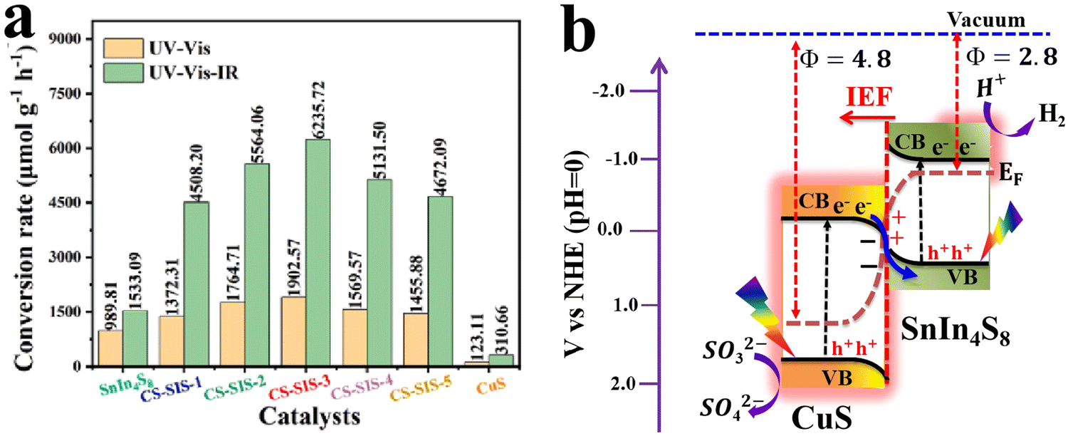 | ||
| Fig. 27 (a) Average photocatalytic H2 production over different CuS catalysts under UV-vis and UV-vis-IR illumination. Reproduced with permission.217 Copyright 2024, Elsevier. (b) Illustration of the charge transfer mechanism over the CuS/SnIn4S8 S-scheme heterojunction. The red glow shows the photothermal effect due to LSPR on CuS. | ||
Apart from sulfide-based photocatalytic materials, CuS is also integrated with metal oxides,260–262 bismuth oxyiodide,222 g-C3N4224 and MOFs223 to construct S-scheme heterojunctions. Due to nonstoichiometric Cu2−xS being a degenerately self-doped p-type semiconductor, it displays a composition-dependent LSPR covering a very broad range from NIR to mid-IR.263 Consequently, its light-harvesting ability can be tailored to cover the entire range of the solar spectrum and develop a full-spectrum-based photocatalyst. In this context, multiple S-scheme photocatalysts based on Cu2−xS have been reported as absorbing the entire UV-vis-NIR light to enhance their photocatalytic activity.
For example, roxbyite (Cu1.8S, CS) with nanoplate (np) and snowflake (sf) morphologies were prepared under solvothermal conditions by varying the sulfur source and subsequently used as the substrate and copper source for the in situ growth of Cu-BDC-NH2 MOF to construct CS/Cu-MOF (CSM) S-scheme heterojunctions.223 The in situ growth synthesis allows for strong bonding and intimate interfacial contact between CS and the Cu MOF that promotes efficient intergranular charge migration separation. The obtained nanocomposite exhibited strong light absorption over the entire solar spectrum benefitting from the unique LSPR of CuS and the distinct absorption features of the Cu-MOF. Therefore, the optimal CSM (sf) hybrid displayed an improved photocatalytic activity with H2 evolution rate of 9343 μmol g−1 h−1 and O2 reduction rate of 2339 μmol g−1 h−1, 14–20 times greater than the pure components. The full spectrum-response property of CuS-based S-scheme systems was also reported for heterojunctions with g-C3N4,224 g-C3N4/Bi2S3250 and VO2.262 Since CuS was used as the OP in most of these studies, the stability is again an important concern with possible activity decline over long-term usage due to surface oxidation and/or photo-corrosion by accumulated photogenerated holes unless a suitable oxidation cocatalyst is attached to boost the on-time photogenerated hole consumption.
6.2.2.1. CuInS2. CuInS2 (CIS) has a narrow direct band gap of ∼1.5 eV, ultrahigh absorption coefficient (1 × 105 cm−1), and negative CB position (∼−0.5 to −1.4 V vs. NHE),265,266 making it an appropriate choice as a RP in S-scheme photocatalysts. Therefore, CIS has been extensively studied in S-scheme configurations with TiO2,267 WO3,225 SnNb2O6,226 Bi2MoO6,268 g-C3N4,229,269,270 Zr-MOF,51 Zn0.5Cd0.5S,227 and ZnIn2S4.228 Composites of CIS are prepared either by the in situ growth approach over the target support or by mixing CIS with the other component in an appropriate solvent followed by evaporating such solvent. For instance, when copper sulfate pentahydrate, indium chloride tetrahydrate, and thiourea (representing CIS precursors) were mixed with a certain amount of WO3 nanosheets and the mixture was transferred to a Teflon-lined autoclave and kept at 433 K for 24 h to allow in situ growth of CIS NSs, a 2D/2D interfacial contact heterojunction was constructed.225 WO3 exhibited a distinct band edge at ∼490 nm, while CIS showed its strong light absorption feature throughout the entire wavelength range. Accordingly, the light-harvesting ability of CIS/WO3 nanocomposites was drastically improved in the visible region compared to that of pure WO3 (Fig. 28a). The catalytic activity of the prepared samples was investigated for degradation of tetracycline hydrochloride (TCH) in a Fenton-like process. CIS/WO3 with an optimum amount of WO3 degraded TCH completely in 6 h (Fig. 28b) and the photocatalyst retains its initial activity even after five successive recycling tests (Fig. 28c). Experimental measurements show that the VB and CB potentials of the n-type WO3 are 2.69 and 0.1 V, while those of the CIS are 1.03 and −0.46 V, respectively, all against RHE. Fig. 28d presents the band structure of the CIS/WO3 nanocomposite. Based on these findings, it is reasonable to conclude that the observed activity cannot be explained in terms of the type-II heterojunction charge transfer mechanism. Instead, the S-scheme configuration rationalizes that the photogenerated electrons and holes responsible for TCH degradation reside on the CIS CB and WO3 VB, respectively.225
 | ||
| Fig. 28 (a) UV-vis DRS profiles of CIS, WO3, and CIS/WO3 hybrid heterostructures with different WO3 contents. (b) Photocatalytic activity of WO3, CIS, and the CIS/WO3 (300 wt%, representing the content of WO3 in the composite) hybrid heterostructure during the photo-Fenton degradation of TCH. (c) Recycling test of the CIS/WO3 composite sample. Reproduced with permission.225 Copyright 2023, Elsevier. (d) Schematic representation of the band structure and charge transfer migration over the CIS/WO3 S-scheme heterojunction. | ||
Importantly, the removal of organic pollutants through oxidative degradation can be combined simultaneously with suitable reduction reactions to make full use of photogenerated electron–hole pairs in both processes of the overall redox reaction. For example, the oxidation of organic pollutants can be accomplished in line with the reduction of Cr(VI) to the less toxic Cr(III). Under these circumstances, the organic pollutant serves as a sacrificial agent to scavenge photogenerated holes, while separated electrons are used to trigger Cr(VI) reduction. Liu and coworkers found that the Cr(VI) reduction efficiency over SnNb2O6/CuInS2 S-scheme heterojunctions was greatly enhanced after introducing TCH as a target organic pollutant and hole scavenger.226 The apparent rate constants for Cr(VI) reduction and TCH oxidation in a mixed pollutant system were increased by 3.74 and 1.58 times, respectively, compared to the mono-pollutant system. This finding indicates that organic pollutants can act as electron donors to consume photoinduced holes and enable more photoexcited electrons to be consumed for photoreduction reactions. The ability of an organic material to support the bi-directional promotion effect is inversely related to its ionization potential (IP), such that pollutants with lower IP indeed have higher electron-donating abilities. Thus, these electron donors possess a higher potential to promote the reduction of the electron acceptor pollutant through the operation of the S-scheme charge migration mechanism.
Alternately, it has been proven that defect engineering is a highly effective approach for enriching surface active sites, enhancing light absorption, and boosting the separation of photogenerated charge carriers.271–273 For example, sulfur vacancy (SV), which is a conventional defect unveiled by metal sulfides, was found to play a role as an active center for promoting reactant adsorption and activation.51,274 When the CIS photocatalyst was allowed to grow over UiO-66-NH2 (UiO-66) using a low-temperature deposition technique, SV was generated in the crystal lattice of CIS. Fig. 29a illustrates the preparation protocol for the UiO-66/CIS composite. The existence of SV was assured by ESR measurements, where a sharp signal at g = 2.004 was attributed to SV. The emergence of SV after the growth of CIS over UiO-66 MOF not only accounts for the improved light absorption and quenched fluorescence, but also for enriching active sites available for adsorption and activation of O2 and N2 gaseous molecules during their respective reduction. Therefore, the optimal UiO-66/CIS20 photocatalyst exhibited notable reduction performances for N2 and O2 with yields of 398 and 4073 μmol g−1 h−1, respectively, 6–20 times higher than those of pure components (Fig. 29b and c). The outstanding activity and excellent stability were assigned to the S-scheme charge transfer action. When UiO-66 is combined with CIS, the staggered band alignment allows for charge migration according to the S-scheme mechanism.
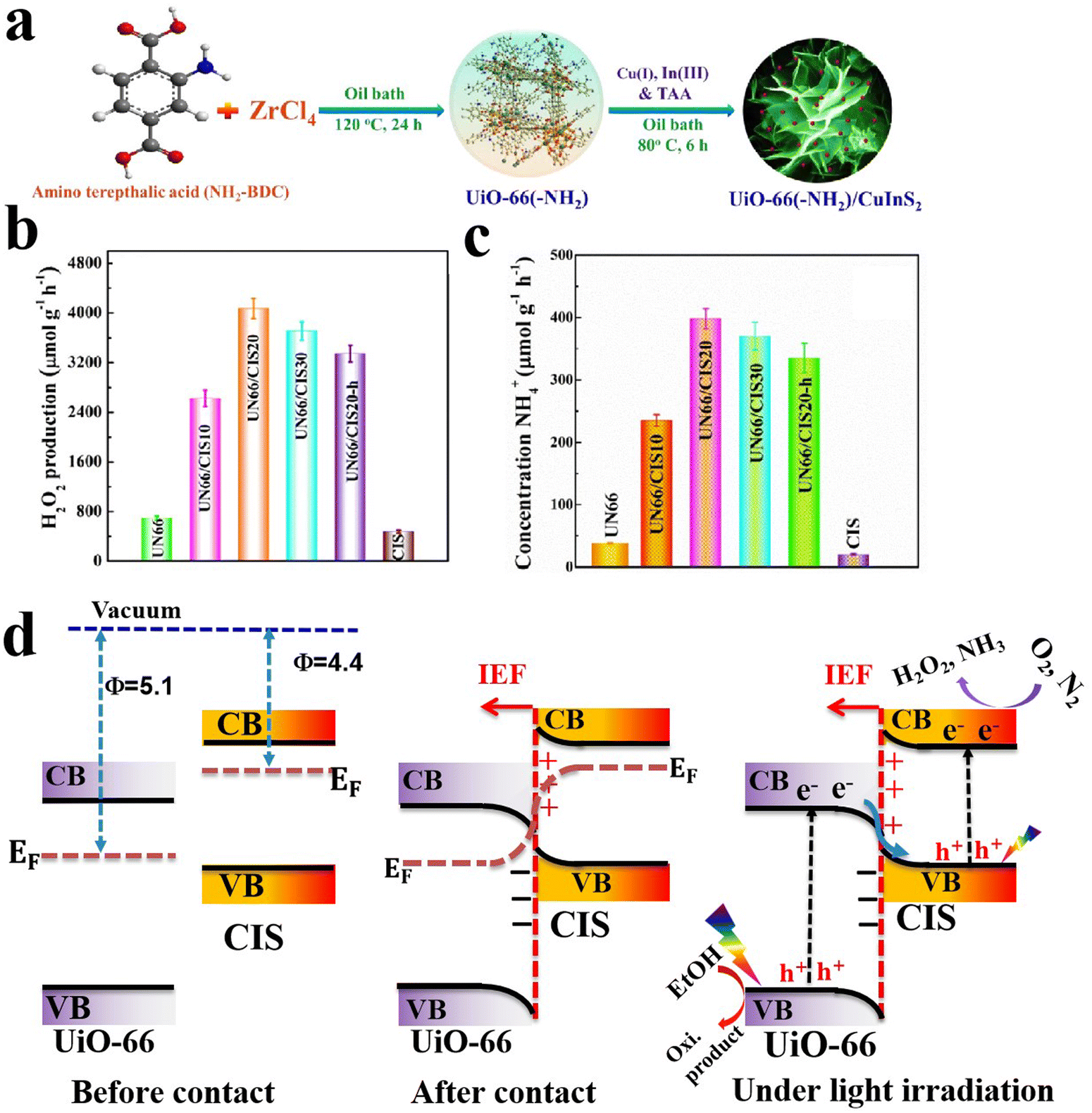 | ||
| Fig. 29 (a) Fabrication of UiO-66/CIS S-scheme heterojunctions. Photocatalytic performances of the prepared catalysts for (b) H2O2 production and (c) N2 fixation. Reproduced with permission.51 Copyright 2023, American Chemical Society. (d) Schematic representation of the band edge potentials of pure CIS and UiO-66 components and plausible S-scheme charge transfer mechanisms in the UiO-66/CIS heterostructures. | ||
Under light illumination, photogenerated electrons and holes with the lower redox potentials become recombined. Meanwhile, most reducing electrons are maintained at the CIS CB to participate in O2 or N2 reduction reactions (Fig. 29d).51 The functional role of SV was also reported for the Zn0.5Cd0.5S/CIS S-scheme heterojunction during H2 evolution reaction.227 These studies shed light on the synergistic effect of atomic vacancy and S-scheme heterojunction systems for photocatalytic applications.
Although defect engineering as a tool to increase the efficiency of conventional photocatalysts (including enhancing light absorption ability, modifying electronic features and improving catalyst reactivity) has been widely appreciated,251,275–277 its specific contributions to S-scheme heterojunctions have been almost overlooked. These include, but are not limited to, enhanced charge separation, longer carrier lifetime, and higher efficiency of surface catalytic reactions. With adequate control over defect type, level, and position, it is possible to tune the charge carrier dynamics and reaction efficiency and even change the charge separation mechanism from type-II to the more favorable S-scheme mechanism. For instance, Xu et al.,272 developed a tunable defect-level-assisted strategy to tailor the OV content in WO3−x/In2S3 S-scheme heterojunctions. The concentration of OVs, along with the induced defect level depth, plays a crucial role in determining the strength of IEF established at the heterojunction interface and thus in the charge separation efficiency. An elevated OV concentration or deep defect levels can lead to excessive charge trapping, which diminishes the charge carrier mobility and worsens photocatalytic activity.278 They found that an intermediate defect level induced by a controlled quantity of OVs in the WO3−x/In2S3 heterojunctions serves as an electron reservoir for effectively prolonging charge carrier lifetimes, promoting the formation of a strong IEF for effective separation of photogenerated electron–hole pairs and hence improving the photocatalytic efficiency. Owing to this distinct role, combined with the extended carrier lifetime, the WO3−x/In2S3 S-scheme heterojunction afforded excellent CO2 photoreduction with nearly 100% CO selectivity. Furthermore, the introduced impurities can adjust the electronic features of the bare semiconductor, enriching the charge carrier concentration in such a way that a switch in the charge transfer mechanism from type-II heterojunction to S-scheme pathway occurs.68 In general, defect engineering has promising potential for designing effective S-scheme heterojunctions and controlling their features such as redox abilities, charge carrier lifetime, and hence reaction efficiency.
6.2.2.2. Cu2WS4. With a narrow bandgap of approximately 2.1 eV, suitable band positions, and co-exposed (101) and (002) crystal facets, Cu2WS4 is a fascinating visible light-responsive photocatalyst. The controlled tuning of the (101) and (002) crystal planes allows for the construction of a homojunction at the interface of these planes, which enhances charge separation under the S-scheme mechanism when integrated with a suitable counterpart. In this way, it is possible to prepare a homojunction/heterojunction system based on Cu2WS4. Due to its distinct set of optical and electronic properties, Cu2WS4 with a predominant (101) facet exhibits strong oxidation ability, while Cu2WS4 with a predominant (002) facet shows a strong reduction ability. The precise control over crystal facets enables the design of Cu2WS4 with desirable electronic and optical properties for targeted applications.230,231,279 For example, Cu2WS4 with a predominant (101) facet was synthesized and used to anchor CdS NPs through a hydrothermal approach.230 The morphology of Cu2WS4 resembles nanoplates with exposed (101) facets (Fig. 30a–c), while CdS NPs are aggregated on the surface of the Cu2WS4 nanoplates (Fig. 30b and c). The light absorption of Cu2WS4 is mainly concentrated in the visible region, with an additional absorption tail extending into the NIR. However, the absorption of the composite sample (CSS10) is further enhanced after CdS is combined with Cu2WS4 (Fig. 30d). According to Tauc plot analysis, the bandgaps of Cu2WS4 and CdS were determined to be approximately 2.13 eV and 2.15 eV, respectively. The composite Cu2WS4/CdS S-scheme heterojunction photocatalyst exhibited H2 evolution activity that was about 21.3 times higher than that of pure CdS and 33.4 times higher than that of Cu2WS4. This improved activity was attributed to the enhanced light absorption and suppressed charge recombination after integrating CdS and Cu2WS4 into an S-scheme configuration (Fig. 30d and e). By considering the CB position of each component (as revealed by M–S measurements), and the work function values based on DFT simulations and band positions, the authors used ISIXPS analysis to support their proposed S-scheme charge migration pathway as depicted in Fig. 30f. When CdS is irradiated, the photogenerated holes are consumed by recombination with electrons from Cu2WS4. Meanwhile, photogenerated holes on Cu2WS4 after light excitation selectively migrate to the (101) crystal facet, which has a higher oxidation potential. Therefore, separated electrons in the CB of CdS are used to drive the HER, while separated holes in the VB of Cu2WS4 are involved in the oxidation reaction.230 Overall, crystal facet engineering can maximize the separation and migration of photogenerated electron–hole pairs, thus promoting the S-scheme charge transfer mechanism and enhancing photocatalytic activity.
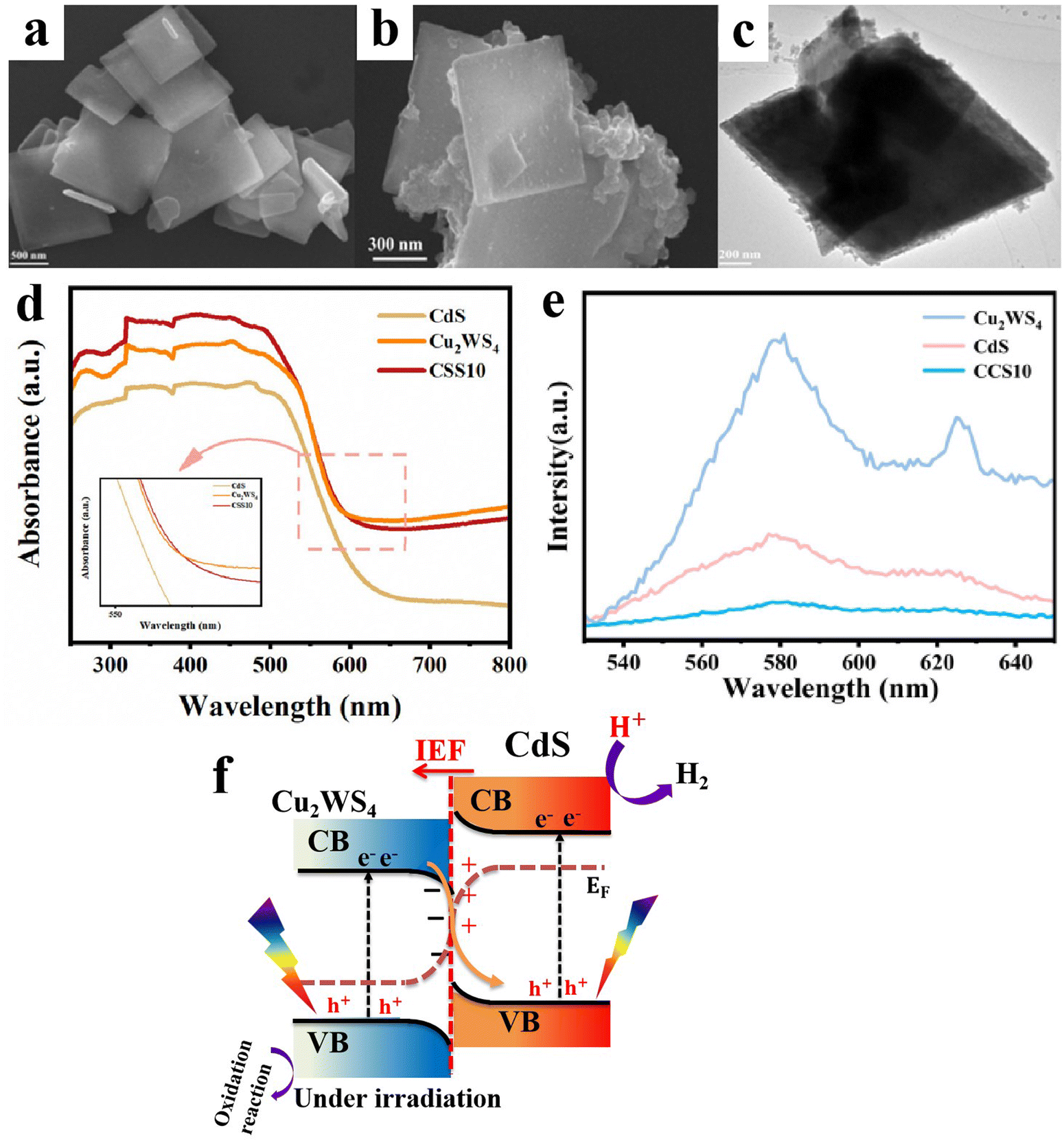 | ||
| Fig. 30 SEM images of (a) Cu2WS4 and (b) Cu2WS4/CdS-10 (CCS10); (c) TEM image of CCS10; DRS (d) and PL curves (e) of the prepared photocatalysts. Reproduced with permission.230 Copyright 2023, Royal Society of Chemistry. (f) Band structure and proposed charge migration pathway over the Cu2WS4/CdS S-scheme heterojunction. | ||
In another study, the ohmic contact established at the plasmonic Au/MoS2 interface further enhances the charge separation across the MoS2/Cu2WS4 heterojunction.231 Therefore, the Cu2WS4/MoS2–Au plasmonic heterojunction follows the S-scheme charge transfer mechanism, enabling photoexcited electrons and holes to achieve the highest reduction and oxidation potentials for efficient Cr(VI) reduction and benzophenone-1 pollutant degradation.
Currently, the integration of Cu2WS4 in S-scheme photocatalytic systems is limited. In addition, detailed information about Cu2WS4 stability during cycling tests still requires careful attention.
6.2.2.3. Other Cu-based binary sulfides. Other Cu-based binary sulfides, including Cu2MoS4 and Cu3SnS4, have also been reported to form S-scheme heterojunctions.233,280 Both compounds can be derived from Cu2O by distinct approaches in the presence of suitable sulfide and Mo- or Sn-precursors. Cu3SnS4 with a highly negative CB at ∼−1.0 V (vs. NHE, pH = 0), and a bandgap of ca. 1.7 eV can be considered a typical RP. Meanwhile, Cu2MoS4, with a bandgap of around 1.9 eV and a CB at approximately −0.55 V (vs. NHE), can function either as an RP or an OP depending on the other component in the S-scheme system.
Saray and his team constructed S-scheme CuSe/Ag-PANI heterojunctions using a simple and cost-effective co-precipitation.234 Multiple phases of CuxSey (CuSe and Cu3Se2) were observed in XRD and HRTEM imaging, suggesting possible formation of dual S-scheme heterojunctions. Namely, a homojunction between different phases of CuSe (since each phase possesses distinct bandgaps and energy edge positions) and a heterojunction between PANI and CuSe. Ag NPs act as an LSPR metal NP, thus strengthening the light absorption extent and as a mediator to boost the migration of photogenerated electrons. Owing to the unique dual S-scheme configuration and the supportive role of plasmonic Ag NPs, the CuxSey/Ag-PANI nanocomposite degraded MB dye completely in just 45 min, compared to 75 min for CuxSey/PANI without Ag NPs. The high negative position of CuSe CB, strong light absorption within the vis-NIR region, and its tailorable structural, optical, and electronic properties greatly support its integration as an effective RP in S-scheme configurations for photo- and photothermal catalytic applications.
6.3. Cu–phosphide
Transition metal phosphides with high conductivity, based on earth abundant elements, and high catalytic activity serve as potential catalytic and/or cocatalytic components in energy-related applications.282 Copper phosphide (Cu3P), which exhibits unique properties such as a narrow bandgap (1.3–1.5 eV), p-type semiconducting behavior and plasmonic response, has recently received increasing interest as a cocatalyst or photocatalyst in heterojunctions.283–286 Due to its excellent electron-accepting ability, Cu3P can be strategically integrated into S-scheme heterojunction configurations to effectively increase the charge transfer and prolong the photoinduced excited electron lifetime for desirable photocatalytic performance.285When combined with TiO2 through a microwave hydrothermal approach, the hydrogen production rate of the Cu3P/TiO2 S-scheme heterojunction with optimum Cu3P loading reached 5.83 mmol g−1 h−1, which was 7.3 and 83.3 times higher than that of pure TiO2 and Cu3P, respectively (Fig. 31a). This S-scheme heterojunction photocatalyst also displayed notable stability over 8 runs (a total of 40 h) of recycling (Fig. 31b). ISIXPS and DFT calculations were used to verify the S-scheme mechanism. Upon light irradiation, ISIXPS showed that the BE of O 1s becomes positively shifted (indicating that O donates electrons), while that of P 2p decreased significantly (corresponding to an electron gain, Fig. 31c and d). Following XPS data, the average charge density calculations based on DFT revealed that electron depletion and accumulation regions are generated, respectively, over Cu3P and TiO2 components (Fig. 31e). These findings firmly support the operation of an S-scheme charge transfer mechanism over the Cu3P/TiO2 heterojunction. Initially, electrons are supposed to move from Cu3P to TiO2 after constructing the heterojunction. Then, photogenerated electrons at the TiO2 CB will be transferred to recombine with holes at the Cu3P VB. The Gibbs free energy (ΔGH*) calculations indicated that Cu centers are the most favorable sites for H+ adsorption (with moderately negative adsorption energy value) (Fig. 31f). Therefore, photogenerated electrons at the Cu3P CB are located properly to accomplish H+ reduction to H2 at Cu sites.235
 | ||
| Fig. 31 (a) Photocatalytic hydrogen production rates of the prepared TiO2, Cu3P and Cu3P/TiO2 with different Cu3P loadings; (b) stability test (8 cycles in 40 h) for hydrogen production over 7.5 wt% Cu3P/TiO2 as a photocatalyst exhibiting the best activity; high-resolution XPS spectra of (c) O 1s and (d) P 2p in Cu3P/TiO2 before and after 1 h illumination; (e) planar average charge density difference between TiO2 and Cu3P (yellow and green colors indicate electron aggregation and depletion regions, respectively); (f) H adsorption Gibbs free energy calculation over different active sites. Reproduced with permission.235 Copyright 2023, Elsevier. | ||
It is noteworthy that the strong atomic interaction between S-scheme heterojunction components at the interface could create interatomic charge transfer channels that facilitate interfacial charge transfer for efficient photogenerated charge carrier separation. For instance, the strong interatomic interaction between oxygen vacancies (OV) in BiOBr and Cu3P not only promotes H2O adsorption at Bi sites, thereby increasing hydrogen production efficiency, but also aids in the migration of photogenerated charge carriers at the interface.286 The newly formed interatomic bonding can fulfill the conditions for better adsorption and activation of reactant molecules.
In another study, Cu3P quantum dots (QDs) of 3–8 nm in size were grafted onto BiOCl NSs to form a 0D/2D heterostructure and tested for TC degradation. The activity measurements showed improved degradation performance of the composite compared to pristine BiOCl. Characterization data confirmed that after the heterojunction formation: (i) photoluminescence (PL) was significantly quenched due to suppressed charge recombination; (ii) enhanced photocurrent was observed due to efficient charge separation; and (iii) pronounced ESR signals for the superoxide radical ˙O2− indicated electron accumulation in the Cu3P CB. All these results infer the potential of Cu3P as a viable alternative for efficient S-scheme heterojunction construction. With a sufficiently negative CB position, Cu3P is well-suited for integration as an RP in S-scheme heterojunctions for better and more stable performances.
Alternatively, phosphosulfides (PS) have received great attention in the catalysis community owing to their structure, which can offer more active sites with better stability than their phosphide or sulfide counterparts.287,288 In this vein, copper phosphosulfide (Cu3P|S) has emerged as a potent photocatalyst for H2 evolution and CO2 reduction.289,290 When 0D Cu3P|S was anchored on 2D g-C3N4 NSs to form a S-scheme heterojunction, interfacial P–N chemical bonds were formed, functioning as electron transfer channels for efficient separation and migration of photogenerated charge carriers. Additionally, the unique PS structure provided abundant active sites for improved CO2 reduction activity. As a result, an enhanced CO generation rate of 137 μmol g−1 h−1 was attained, which is 8 and 2.3 times higher than that of pristine g-C3N4 and Cu3P/g-C3N4, respectively.289 Although Cu3P and Cu3P|S are emerging Cu-based photocatalysts, reports on their integration into S-scheme heterojunctions are still scarce. Therefore, future studies are encouraged to further explore their potential in photocatalytic applications. Interestingly, the SPR response of these materials can be exploited for NIR photocatalysis or photothermal catalysis.
6.4. Cu-MOF
As previously discussed in Section 5.1.1.6, MOFs are porous crystalline materials with a wide range of chemical compositions and they exhibit tunable optical and electronic features, thereby promoting their wide application in photocatalysis. Other photocatalytic scaffolds can be confined within the 3D porous structure of MOFs, allowing for the establishment of strong interfacial contact for accessible charge transfer, and enhancing photocatalytic activity. Following this scenario, Cao et al.,239 anchored Mn0.05Cd0.95S NPs over Cu-BTC MOF regular octahedrons for H2 evolution applications. Benefiting from the high surface area of Cu-MOFs with a high density of active sites and the S-scheme charge transfer mechanism at the interface, the H2 evolution activity under LED irradiation was doubled compared to that of pristine Mn0.05Cd0.95S. When the composition was changed to Zn0.5Cd0.5S, the H2 evolution performance drastically increased to 18986 μmol g−1 h−1 for the Zn0.5Cd0.5S/Cu-MOF octahedron composite, tested under a 300 W Xe lamp.240 Although light intensity is a key factor for the observed photocatalytic activity, normalizing photocatalytic performance using metrics such as the apparent quantum efficiency (AQE) could allow for a more reasonable comparison of results and provide a clearer outlook on current achievements and prospects.
Cu-BTC has been integrated with other inorganic semiconductors such as ZnWO4 and CuInS2 to construct S-scheme heterojunctions with improved activity and stability.45,238 In these systems, the Cu-BTC MOF exhibited an n-type semiconducting behavior with a large bandgap of ∼2.8 eV, CB located at ∼−0.55 V (vs. NHE), and a highly positive VB position. Thereby, it functioned as an OP.
Porphyrin is a typical photosensitizer with high visible light absorption and a long-lived excited state.291,292 Porphyrin-based MOFs combine the benefits of both porphyrin and MOF, particularly supporting superior electron mobility due to the localization of electrons over an extended π-conjugated system composed of macrocycles. An ultrathin 2D Cu-meso-tetrakis(4-carboxyphenyl)porphyrin (TCPP) MOF is a prime example of porphyrin-based MOFs, showing promising potential for CO2 reduction due to its abundant active sites, which favor the adsorption and activation of CO2 molecules. When combined with oxygen vacancy-rich CeO2 (LA-CeO2) prepared following a mild solvothermal synthesis, a unique 0D/2D S-scheme heterojunction structure was constructed (Fig. 32a–e).241 The morphology of Cu-TCPP MOF is ultrathin NSs (Fig. 32b), while monodispersed CeO2 NPs with an average diameter of 22 nm were deposited on them (Fig. 32c and d). Compared with the light absorption of CeO2, which is mainly concentrated in the UV region, CeO2@Cu-TCPP nanocomposites exhibited excellent light-harvesting ability across the entire UV-vis-NIR region due to various allowed electronic transitions localized on the TCPP moieties. Owing to the strong absorption in the NIR, the CeO2@Cu-TCPP nanocomposites displayed a prominent photothermal response as revealed by thermal images taken after light irradiation. CeO2@Cu-TCPP with optimum CeO2 loading showed remarkable photocatalytic CO2 reduction activity, with CO and CH4 yields of 229.6 and 13.85 μmol g−1 after 4 h, which were orders of magnitude higher than those of pristine CeO2 and Cu-TCPP.
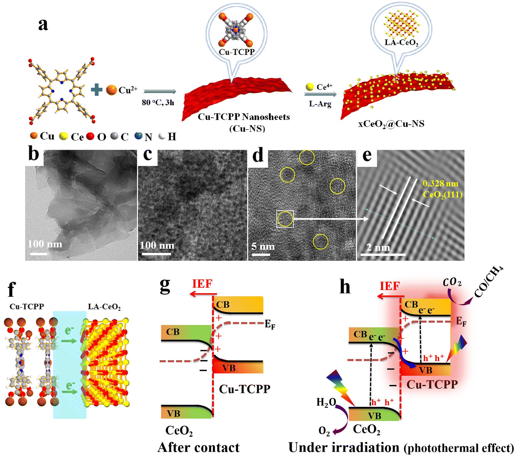 | ||
| Fig. 32 (a) Schematic of the preparation procedure of the Cu-TCPP MOF and CeO2/Cu-CTPP S-scheme heterojunction. TEM of Cu-TCPP 2D NSs (b) and single CeO2 NP (c); HRTEM (d) and FFT image (e) of CeO2@Cu-TCPP; (f) Electron flow direction within the 0.25CeO2@Cu-TCPP S-scheme heterojunction photocatalyst; reproduced with permission.241 Copyright 2023, American Chemical Society. Schematic illustration of the charge transfer mechanism of the CeO2@Cu-TCPP S-scheme heterojunction after contact (g) and under light (h). | ||
The enhanced activity and stability of CeO2@Cu-TCPP were attributed to several factors including (i) a higher content of OVs and hydrophilic –OH groups, which endowed the sample with sufficient active sites for favorable adsorption and activation of CO2 molecules and accessible mass/charge transfer; (ii) the S-scheme heterojunction established at the n–n type heterojunction that allows electron diffusion from Cu-TCPP to CeO2 after contact and until equilibrium (Fig. 32f and g) and maintains the most valuable photogenerated electrons and holes with higher redox potential to participate efficiently in the targeted reactions. The photothermal effect also contributed positively to the overall charge separation process (Fig. 32h).
As the study pointed out the potential of the Cu-TCPP MOF as a promising 2D photocatalytic component for constructing S-scheme systems, it also highlighted the cumulative function of surface modification, defect engineering, and heterojunction construction toward improving the performance and stability of a photocatalytic system. Table 6 summarizes most S-scheme systems incorporating Cu-MOF as a photocatalytic component.
In this regard, it is important to emphasize the unique features of the 2D materials such as large surface area and thin layered structure. Such peculiar morphology is pivotal for shortening the required diffusion length of charge carriers to react, improved reagent mass transfer and full exposure of the active sites for target photocatalytic reactions. Additionally, the layered morphology favors intimate interfacial contact, thus providing accessible channels for photoinduced charge carrier transfer through the interface and hence better reaction efficiency derived from more efficient charge separation.30,293,294 Different combinations based on 2D photocatalytic materials can be designed to fulfill the S-scheme heterojunction perquisites including 0D/2D, 1D/2D and 2D/2D heterojunctions. Excellent reviews summarizing recent progress on 2D materials and their integration in S-scheme heterojunction systems can be found in the literature.7,30
Apart from the 0D/2D configurations discussed in the previous section, the 2D/2D heterojunctions possess ample merits such as (i) the “face-to-face” contact, enabling an extended interface with better interfacial matching for enhanced charge migration, and (ii) strong electronic coupling between layers, optimizing the electronic structure of the constituent 2D materials for improved catalytic activity.242,295–297 Various 2D scaffolds, including g-C3N4, graphdiyne, phosphorene, MXenes, 2D MOFs, 2D COFs, and transition metal dichalcogenides, are readily available and confer interest for a versatile family of functional heterojunction materials. Among them, COFs represent a class of porous covalent polymers with high specific surface area, adequate crystallinity, tunable composition, broad light absorption ability, and excellent electron mobility over the extended π-conjugated framework. Under these features, COFs are well-suited candidates for photocatalysis.298–301 Recently, Hu et al.,242 took advantage of 2D/2D MOF/COF structures to construct a fascinating photocatalytic system for H2 evolution. Besides the S-scheme charge transfer mechanism, the long-range ordered crystalline structure of both components with a 2D/2D interface contributed markedly to guided charge transfer. The extremely high specific surface area of the integrated materials provided abundant active sites for H+ adsorption and reduction. All these factors contributed to the commendable photocatalytic activity and stability of the Cu-MOF/COF heterostructure.
Although these results are promising, the integration of Cu-MOFs in S-scheme heterojunctions for photocatalytic applications is still limited. COF/MOF-based S-scheme heterojunction photocatalysts are expected to attract considerable interest in future research due to the vast chemical space available for these hybrid composites that allow the design and fine tuning of their optoelectronic properties.
7. Conclusions and perspectives
The construction of S-scheme heterojunctions offers a compelling approach not only for the effective separation of photogenerated charge carriers but also for preserving charges with the highest redox potential at distinct locations. This approach alleviates the challenge of charge recombination and strongly enhances reaction kinetics. In this context, Cu-based photocatalytic materials, including a wide range of compounds such as oxides, binary oxides, chalcogenides, phosphides, and MOFs, form a versatile family of efficient components for S-scheme heterojunction construction. In this review, we summarized recent progress in the development of S-scheme heterojunctions involving Cu-based photocatalytic materials.With their narrow bandgaps implying absorption of a wide range of visible light radiation, suitable band positions implying that they can promote useful reduction and some oxidation reactions, and unique structural, optical, and electronic properties, these materials offer multiple opportunities for optimizing the activity, selectivity, and stability of photocatalytic systems for various target applications. The charge separation efficiency, and consequently the activity, can be further enhanced by modifying these materials with cocatalytic moieties such as metallic clusters, carbonaceous materials, and conductive 2D substrates. Newly emerging 2D materials, including MXenes, GDY, and phosphorene, exhibit fascinating electrical conductivity and surface activity, making them excellent candidates for integration into S-scheme systems.
Moreover, constructing strongly interconnected components, even with interfacial covalent bonds and hybridized electronic states can facilitate the appearance of charge transfer channels at the interface, enabling efficient charge carrier migration. In this regard, in situ generation methods have proven effective in forming covalent bonds between the components of S-scheme heterojunctions. For example, the formation of Cu–S covalent bonds upon integrating CuO with ZnIn2S4 has been found to open accessible pathways for enhanced charge separation and restructure of the electronic arrangement of reacting molecules.
Cu-based photocatalytic materials exhibit a wide range of electronic properties, enabling them to act as either RP or OP depending on their band positions and stability under reaction conditions. Some Cu-chalcogenides and Cu-MOFs exhibit dual functionality as both the RP and OP due to their appropriate band positions. The stability of S-scheme heterojunctions is further enhanced by the spatial separation of electron–hole pairs. For instance, Cu2O is unstable when used as an OP due to oxidation by accumulated photogenerated holes. Therefore, Cu2O is better suited for integration as an RP in S-scheme systems to ensure sustainable performance. In this regard, it has been proposed in some cases that the Cu2+/Cu+ redox pair plays a crucial role in the adsorption and activation of reactant molecules, particularly in pollutant degradation. The partial reduction of Cu2+ to Cu+ by photogenerated electrons sustains the catalytic cycle in Fenton-like processes, maintaining system activity without the need for external reducing agents.
A variety of photophysical and theoretical approaches have been adopted to study the charge transfer mechanisms within S-scheme heterojunctions. Techniques such as ISIXPS and DFT calculations are widely used to confirm the S-scheme charge transfer mechanism, while fs-TAS is a powerful tool for measuring the lifetime of charge carriers. The extension of charge carrier lifetime or the appearance of new charge transfer processes with distinct lifetimes following heterojunction formation can indicate efficient charge transfer. Advanced characterization techniques with sufficient temporal and spatial resolution need to be further developed to identify active sites and optimize the activity and stability of these photocatalytic systems.
This review has provided an overview of the current progress in the field, with the aim of guiding future research toward the development of novel, high-performance Cu-based S-scheme photocatalysts and a deeper understanding of their underlying photocatalytic mechanisms. However, there remains significant potential to explore the broader integration of these materials into S-scheme heterojunctions trying to overcome the current bottlenecks in the areas related to efficiency and stability. In particular, Cu3P and Cu-binary sulfides are promising candidates with unique properties, yet their integration into S-scheme photocatalytic systems has been scarcely studied.
The S-scheme heterojunction photocatalytic system is a rapidly emerging field in the realm of catalysis and is expected to continue to gain prominence. Interest in Cu-based S-scheme heterojunctions is anticipated to grow in the near future, as researchers work to develop photocatalytic systems based on earth-abundant elements. These advancements could bring the commercial production of solar fuels and chemicals closer to reality, helping to meet global energy and environmental demands.
Data availability
No primary research results, software or code have been included and no new data were generated or analysed as part of this review.Conflicts of interest
There are no conflicts to declare.Acknowledgements
The authors acknowledge the financial support from the National Key Research and Development Program of China (2022YFB3803600); the National Natural Science Foundation of China (W2433135, 22361142704, 22238009, 22261142666 and U23A20102); the Natural Science Foundation of Hubei Province, China (2022CFA001 and 2023AFA088); the Spanish Ministry of Science and Innovation (CEX2021-01230-S and PDI2021-0126071-OB-CO21 funded by MCIN/AEI/10.13039/501100011033) and Generalitat Valenciana (Prometeo 2021/038 and Adv Mater programme Graphica MFA/2022/023 with funding from European Union NextGenerationEU PRTR-C17.I1); this work was also supported by the Fundamental Research Funds for the Central Universities, China University of Geosciences (Wuhan) (no. CUG22061).References
- B. Wang, G. M. Biesold, M. Zhang and Z. Lin, Chem. Soc. Rev., 2021, 50, 6914–6949 RSC.
- H. Mai, D. Chen, Y. Tachibana, H. Suzuki, R. Abe and R. A. Caruso, Chem. Soc. Rev., 2021, 50, 13692–13729 RSC.
- P. Kumar, G. Singh, X. Guan, J. Lee, R. Bahadur, K. Ramadass, P. Kumar, Md. G. Kibria, D. Vidyasagar, J. Yi and A. Vinu, Chem. Soc. Rev., 2023, 52, 7602–7664 RSC.
- Y. Shi, Z. Zhao, D. Yang, J. Tan, X. Xin, Y. Liu and Z. Jiang, Chem. Soc. Rev., 2023, 52, 6938–6956 RSC.
- X. Tao, Y. Zhao, S. Wang, C. Li and R. Li, Chem. Soc. Rev., 2022, 51, 3561–3608 Search PubMed.
- Z. Wang, Y. Hu, S. Zhang and Y. Sun, Chem. Soc. Rev., 2022, 51, 6704–6737 Search PubMed.
- B. Zhu, J. Sun, Y. Zhao, L. Zhang and J. Yu, Adv. Mater., 2024, 36, 2310600 Search PubMed.
- M. J. Molaei, J. Am. Ceram. Soc., 2024, 107, 5695–5719 CrossRef.
- K. Sharma, V. Hasija, M. Malhotra, P. K. Verma, A. A. Parwaz Khan, S. Thakur, Q. Van Le, H. H. Phan Quang, V.-H. Nguyen, P. Singh and P. Raizada, Int. J. Hydrogen Energy, 2024, 52, 804–818 CrossRef.
- S. Wageh, A. A. Al-Ghamdi, R. Jafer, X. Li and P. Zhang, Chin. J. Catal., 2021, 42, 667–669 CrossRef.
- Q. Xu, L. Zhang, B. Cheng, J. Fan and J. Yu, Chem, 2020, 6, 1543–1559 Search PubMed.
- J. Low, J. Yu, M. Jaroniec, S. Wageh and A. A. Al-Ghamdi, Adv. Mater., 2017, 29, 1601694 CrossRef PubMed.
- L. Wang, B. Zhu, J. Zhang, J. B. Ghasemi, M. Mousavi and J. Yu, Matter, 2022, 5, 4187–4211 CAS.
- L. Wang, J. Sun, B. Cheng, R. He and J. Yu, J. Phys. Chem. Lett., 2023, 14, 4803–4814 CrossRef CAS PubMed.
- A. J. Bard, J. Photochem., 1979, 10, 59–75 CAS.
- L. Wang, C. Bie and J. Yu, Trends Chem., 2022, 4, 973–983 CAS.
- J. Low, C. Jiang, B. Cheng, S. Wageh, A. A. Al-Ghamdi and J. Yu, Small Methods, 2017, 1, 1700080 Search PubMed.
- H. Tada, T. Mitsui, T. Kiyonaga, T. Akita and K. Tanaka, Nat. Mater., 2006, 5, 782–786 CAS.
- Q. Xu, L. Zhang, J. Yu, S. Wageh, A. A. Al-Ghamdi and M. Jaroniec, Mater. Today, 2018, 21, 1042–1063 CAS.
- J. Yu, S. Wang, J. Low and W. Xiao, Phys. Chem. Chem. Phys., 2013, 15, 16883–16890 CAS.
- J. Fu, Q. Xu, J. Low, C. Jiang and J. Yu, Appl. Catal., B, 2019, 243, 556–565 CrossRef CAS.
- F. Li, G. Zhu, J. Jiang, L. Yang, F. Deng, Arramel and X. Li, J. Mater. Sci. Technol., 2024, 177, 142–180 CAS.
- X. Wang, M. Sayed, O. Ruzimuradov, J. Zhang, Y. Fan, X. Li, X. Bai and J. Low, Appl. Mater. Today, 2022, 29, 101609 Search PubMed.
- Q. Xu, S. Wageh, A. A. Al-Ghamdi and X. Li, J. Mater. Sci. Technol., 2022, 124, 171–173 Search PubMed.
- C. Bie, B. Zhu, L. Wang, H. Yu, C. Jiang, T. Chen and J. Yu, Angew. Chem., Int. Ed., 2022, 61, e202212045 CAS.
- X. Wu, G. Chen, J. Wang, J. Li and G. Wang, Acta Phys.-Chim. Sin., 2023, 39, 2212016 Search PubMed.
- S. Rej, M. Bisetto, A. Naldoni and P. Fornasiero, J. Mater. Chem. A, 2021, 9, 5915 CAS.
- L. Zhang, J. Zhang, H. Yu and J. Yu, Adv. Mater., 2022, 34, 2107668 CAS.
- B. Zhu, C. Jiang, J. Xu, Z. Zhang, J. Fu and J. Yu, Mater. Today, 2025, 82, 251–273 CAS.
- W. Wang, B. Cheng, G. Luo, J. Yu and S. Cao, Mater. Today, 2024, 81, 137–158 CAS.
- M. Sayed, B. Zhu, P. Kuang, X. Liu, B. Cheng, A. A. Al Ghamdi, S. Wageh, L. Zhang and J. Yu, Adv. Sustainable Syst., 2022, 6, 2100264 CAS.
- M. Sabir, M. Sayed, Z. Zeng, B. Cheng, W. Wang, C. Wang, J. Xu and S. Cao, Appl. Surf. Sci., 2025, 693, 162752 CAS.
- A. Zindrou, L. Belles and Y. Deligiannakis, Solar, 2023, 3, 87–112 Search PubMed.
- S. Gorsse, M. Gouné, W.-C. Lin and L. Girard, Sci. Data, 2023, 10, 504 CrossRef CAS.
- M. B. Gawande, A. Goswami, F.-X. Felpin, T. Asefa, X. Huang, R. Silva, X. Zou, R. Zboril and R. S. Varma, Chem. Rev., 2016, 116, 3722–3811 CrossRef CAS PubMed.
- R. Zhang, Y. Chen, M. Ding and J. Zhao, Nano Res., 2022, 15, 2810–2833 CrossRef.
- Y. Du, Y.-T. Tang, X. Ma, J. Li and Q. Guo, Cryst. Growth Des., 2024, 24, 2592–2618 CrossRef.
- H. Xie, J. Wang, K. Ithisuphalap, G. Wu and Q. Li, J. Energy Chem., 2017, 26, 1039–1049 Search PubMed.
- J. Xia, X. Liu, H. Zhou, L. Pu, J. Zhang, X. Li, F. Li, L. Long, S. Li and Y. He, Catal. Sci. Technol., 2021, 11, 7905–7913 Search PubMed.
- D. Derelli, F. Caddeo, K. Frank, K. Krötzsch, P. Ewerhardt, M. Krüger, S. Medicus, L. Klemeyer, M. Skiba, C. Ruhmlieb, O. Gutowski, A.-C. Dippel, W. J. Parak, B. Nickel and D. Koziej, Angew. Chem., Int. Ed., 2023, 62, e202307948 Search PubMed.
- M. Balık, V. Bulut and I. Y. Erdogan, Int. J. Hydrogen Energy, 2019, 44, 18744–18755 Search PubMed.
- K. Jagadish, A. Godha, B. Pandit, Y. Jadhav, A. Dutta, J. Satapathy, H. Bhatt, B. Singh, S. K. Makineni, S. Pal and S. R. Rondiya, Small, 2024, 20, 2405859 CrossRef PubMed.
- A. Rahman, J. R. Jennings and M. M. Khan, Mater. Sci. Semicond. Process., 2024, 169, 107930 Search PubMed.
- Y.-Q. Liu, F.-X. Wang, Y. Xiao, H.-D. Peng, H.-J. Zhong, Z.-H. Liu and G.-B. Pan, Sci. Rep., 2014, 4, 5998 CrossRef PubMed.
- J. S. Jeyaprakash, M. Rajamani, C. L. Bianchi, M. Ashokkumar and B. Neppolian, Ultrason. Sonochem., 2023, 100, 106624 Search PubMed.
- M. Haddad, A. Belhadi, L. Boudjellal and M. Trari, Int. J. Hydrogen Energy, 2021, 46, 37556–37563 Search PubMed.
- F. Nekouei, S. Nekouei, M. Pouzesh and Y. Liu, Chem. Eng. J., 2020, 385, 123710 CrossRef.
- T. Xiang, F. Xin, C. Zhao, S. Lou, W. Qu, Y. Wang, Y. Song, S. Zhang and X. Yin, J. Colloid Interface Sci., 2018, 518, 34–40 Search PubMed.
- H. Wu, X. Y. Kong, X. Wen, S.-P. Chai, E. C. Lovell, J. Tang and Y. H. Ng, Angew. Chem., Int. Ed., 2021, 60, 8455–8459 CrossRef PubMed.
- M. Sayed, L. Zhang and J. Yu, Chem. Eng. J., 2020, 397, 125390 Search PubMed.
- R. Bariki, S. K. Pradhan, S. Panda, S. K. Nayak, A. R. Pati and B. G. Mishra, Langmuir, 2023, 39, 7707–7722 CrossRef PubMed.
- K. Meng, J. Zhang, B. Cheng, X. Ren, Z. Xia, F. Xu, L. Zhang and J. Yu, Adv. Mater., 2024, 36, 2406460 Search PubMed.
- D. Gholami, S. Shahbazi, S. Mosleh, A. Ghoorchian, S. Hajati, K. Dashtian and G. Yasin, Chem. Eng. J., 2023, 461, 141950 Search PubMed.
- H. Hamad, M. M. Elsenety, W. Sadik, A.-G. El-Demerdash, A. Nashed, A. Mostafa and S. Elyamny, Sci. Rep., 2022, 12, 2217 CAS.
- Q.-Y. Tang, W.-F. Chen, Y.-R. Lv, S.-Y. Yang and Y.-H. Xu, Sep. Purif. Technol., 2020, 236, 116243 CAS.
- R. He, D. Xu and M. Sayed, J. Materiomics, 2025, 11, 100989 CrossRef.
- J. Zhang, B. Zhu, L. Zhang and J. Yu, Chem. Commun., 2023, 59, 688–699 RSC.
- W. Melitz, J. Shen, A. C. Kummel and S. Lee, Surf. Sci. Rep., 2011, 66, 1–27 CrossRef CAS.
- C. Cheng, B. He, J. Fan, B. Cheng, S. Cao and J. Yu, Adv. Mater., 2021, 33, 2100317 Search PubMed.
- J.-X. Shen, J. M. Munro, M. K. Horton, P. Huck, S. Dwaraknath and K. A. Persson, Sci. Data, 2022, 9, 661 Search PubMed.
- D. Liu, L. Jiang, D. Chen, Z. Hao, B. Deng, Y. Sun, X. Liu, B. Jia, L. Chen and H. Liu, Chem. Eng. J., 2024, 482, 149165 CrossRef CAS.
- B. He, Z. Wang, P. Xiao, T. Chen, J. Yu and L. Zhang, Adv. Mater., 2022, 34, 2203225 CrossRef CAS.
- C. Cheng, J. Zhang, B. Zhu, G. Liang, L. Zhang and J. Yu, Angew. Chem., Int. Ed., 2023, 62, e202218688 CrossRef CAS.
- X. Deng, J. Zhang, K. Qi, G. Liang, F. Xu and J. Yu, Nat. Commun., 2024, 15, 4807 CrossRef CAS PubMed.
- L. Li, C. Guo, T. Li, C. Yang, F. Chen, W. Wang, R. Yan, J. Ning and Y. Hu, Appl. Surf. Sci., 2024, 651, 159220 CrossRef CAS.
- J. Li, J. Guo, J. Zhang, Z. Sun and J. Gao, Surf. Interfaces, 2022, 34, 102308 CrossRef CAS.
- L. Qi, M. Wang, J. Xue, Q. Zhang, F. Chen, Q. Liu, W. Li and X. Li, Chem. – Eur. J., 2021, 27, 14638–14644 CrossRef PubMed.
- K. Huang, G. Liang, S. Sun, H. Hu, X. Peng, R. Shen and X. Li, J. Mater. Sci. Technol., 2024, 193, 98–106 CrossRef.
- B. H. Park, H. Park, T. Kim, S. J. Yoon, Y. Kim, N. Son and M. Kang, Int. J. Hydrogen Energy, 2021, 46, 38319–38335 CrossRef.
- V. Soni, Sonu, P. Singh, S. Thakur, P. Thakur, T. Ahamad, V.-H. Nguyen, Q. Van Le, C. M. Hussain and P. Raizada, J. Environ. Chem. Eng., 2023, 11, 110856 CrossRef.
- P. Mandyal, R. Sharma, S. Sambyal, N. Islam, A. Priye, M. Kumar, V. Chauhan and P. Shandilya, J. Water Process Eng., 2024, 59, 105008 CrossRef.
- Q. Chen, L. Hu, Y. Shi, C. Liu, Y. Hou, J. Bi, J. C. Yu and L. Wu, Chemosphere, 2024, 352, 141446 CrossRef PubMed.
- W. Shi, J. C. Wang, A. Chen, X. Xu, S. Wang, R. Li, W. Zhang and Y. Hou, Nanomaterials, 2022, 12, 2284 Search PubMed.
- D. Cui, S. Wang, X. Yang, L. Xu and F. Li, Small, 2024, 20, 2306229 CrossRef PubMed.
- L. Zhang, Y. Wu, N. Tsubaki and Z. Jin, Acta Phys.-Chim. Sin., 2023, 39, 2302051 Search PubMed.
- T. Ying, W. Liu, L. Yang, S. Zhang, Z. Wu, J. Li, R. Song, W. Dai, J. Zou and S. Luo, Sep. Purif. Technol., 2024, 330, 125272 CrossRef.
- Z. Li, S. Ye, P. Qiu, X. Liao, Y. Yao, J. Zhang, Y. Jiang and S. Lu, Dalton Trans., 2022, 51, 10578–10586 RSC.
- S. Arasavilli, P. A. Taksal, B. Kanti Das, S. Chowdhury and J. Bhattacharya, J. Environ. Chem. Eng., 2024, 12, 112703 CrossRef.
- J. Huang, H. Shi, X. Wang, P. Wang, F. Chen and H. Yu, Catal. Sci. Technol., 2024, 14, 2514–2521 RSC.
- D. Tang, D. Xu, Z. Luo, J. Ke, Y. Zhou, L. Li and J. Sun, Nanomaterials, 2022, 12, 2455 CrossRef PubMed.
- C. Yan, M. Xu, W. Cao, Q. Chen, X. Song, P. Huo, W. Zhou and H. Wang, J. Environ. Chem. Eng., 2023, 11, 111479 CrossRef.
- M. Gao, W. Li, X. Su, Z. Li, X. Ding, X. Du, Y. Ren, H. Zhang, J. Feng and T. Wei, Sep. Purif. Technol., 2023, 313, 123447 CrossRef.
- X. Yuan, J. Yang, Y. Yao, H. Shen, Y. Meng, B. Xie, Z. Ni and S. Xia, Sep. Purif. Technol., 2022, 291, 120965 CrossRef.
- J. C. Wang, X. Qiao, W. Shi, J. He, J. Chen and W. Zhang, Acta Phys.-Chim. Sin., 2023, 39, 2210003 Search PubMed.
- L. Fan, J. Han, K. Wei, C. Ma, S. Feng, Y. Zhou, X. Dai, Z. Ye and Y. Wang, J. Alloys Compd., 2023, 960, 170382 CrossRef CAS.
- K. Huang, B. Feng, X. Wen, L. Hao, D. Xu, G. Liang, R. Shen and X. Li, Chin. J. Struct. Chem., 2023, 42, 100204 CrossRef CAS.
- J. Liu, F. Qi, N. Zhang, J. Yang, Z. Liang, C. Tian, W. Zhang, X. Tang, D. Wu and Q. Huang, J. Mater. Sci., 2022, 57, 15474–15487 CrossRef CAS.
- B. Dai, Y. Li, J. Xu, C. Sun, S. Li and W. Zhao, Appl. Surf. Sci., 2022, 592, 153309 CrossRef CAS.
- B. Dai, W. Zhao, W. Wei, J. Cao, G. Yang, S. Li, C. Sun and D. Y. C. Leung, Carbon, 2022, 193, 272–284 CrossRef CAS.
- F. Mu, X. Miao, J. Cao, W. Zhao, G. Yang, H. Zeng, S. Li and C. Sun, J. Cleaner Prod., 2022, 360, 131948 CAS.
- L. W. Wei, S. H. Liu and H. P. Wang, ACS Appl. Mater. Interfaces, 2023, 15, 25473–25483 CAS.
- J. Wang, S. Li, P. Ma, Z. Guo, Q. Ma, Q. Zhao, Y. Guo, J. Zhao and G. Guan, Colloids Surf., A, 2024, 690, 133779 CAS.
- P. Qiao, X. Wang, M. Dai, R. Piao, H. Liu, W. Wang, Y. Wang and H. Song, Mater. Lett., 2024, 359, 135923 CAS.
- B. He, P. Xiao, S. Wan, J. Zhang, T. Chen, L. Zhang and J. Yu, Angew. Chem., Int. Ed., 2023, 62, e202313172 CAS.
- L. Xu, H. L. An, X. Q. Wu, W. T. Ju, Y. Wang, X. F. Wang and X. Wang, Surf. Interfaces, 2023, 41, 103202 CAS.
- M. N. Gordon, K. Chatterjee, N. Christudas Beena and S. E. Skrabalak, ACS Sustainable Chem. Eng., 2022, 10, 15622–15641 CAS.
- X. Wei, M. U. Akbar, A. Raza and G. Li, Nanoscale Adv., 2021, 3, 3353–3372 CAS.
- J. Di, J. Xia, H. Li, S. Guo and S. Dai, Nano Energy, 2017, 41, 172–192 CAS.
- R. Suresh, S. Rajendran, P. S. Kumar, T. K. A. Hoang and M. Soto-Moscoso, Environ. Res., 2022, 212, 113149 CAS.
- X. Dou, C. Zhang and H. Shi, Sep. Purif. Technol., 2022, 282, 120023 CAS.
- S. S. Imam, R. Adnan and N. H. Mohd Kaus, J. Environ. Chem. Eng., 2021, 9, 105404 CAS.
- X. Li, J. Xiong, X. Gao, J. Ma, Z. Chen, B. Kang, J. Liu, H. Li, Z. Feng and J. Huang, J. Hazard. Mater., 2020, 387, 121690 CAS.
- K. Xie, S. Xu, K. Xu, W. Hao, J. Wang and Z. Wei, Chemosphere, 2023, 317, 137823 CrossRef CAS PubMed.
- C. Y. Wang, X. Zhang and H. Q. Yu, Coord. Chem. Rev., 2023, 493, 215339 CrossRef CAS.
- X. Wei, M. U. Akbar, A. Raza and G. Li, Nanoscale Adv., 2021, 3, 3353–3372 RSC.
- Y. Li, H. Jiang, X. Wang, X. Hong and B. Liang, RSC Adv., 2021, 11, 26855–26875 RSC.
- Y. Song, X. Zheng, Y. Yang, Y. Liu, J. Li, D. Wu, W. Liu, Y. Shen and X. Tian, Adv. Mater., 2024, 36, 2305835 CrossRef CAS PubMed.
- Q. Zhong, Y. Li and G. Zhang, Chem. Eng. J., 2021, 409, 128099 CrossRef CAS.
- P. Kuang, J. Low, B. Cheng, J. Yu and J. Fan, J. Mater. Sci. Technol., 2020, 56, 18–44 CrossRef CAS.
- F. He, B. Zhu, B. Cheng, J. Yu, W. Ho and W. Macyk, Appl. Catal., B, 2020, 272, 119006 CrossRef CAS.
- J. Low, L. Zhang, T. Tong, B. Shen and J. Yu, J. Catal., 2018, 361, 255–266 CrossRef CAS.
- J. Liu, F. Qi, N. Zhang, J. Yang, Z. Liang, C. Tian, W. Zhang, X. Tang, D. Wu and Q. Huang, J. Mater. Sci., 2022, 57, 15474–15487 CrossRef CAS.
- S. Sahani, K. Malika Tripathi, T. Il Lee, D. P. Dubal, C.-P. Wong, Y. Chandra Sharma and T. Young Kim, Energy Convers. Manage., 2022, 252, 115133 CrossRef CAS.
- C. M. Pelicano, J. Li, M. Cabrero-Antonino, I. F. Silva, L. Peng, N. V. Tarakina, S. Navalón, H. García and M. Antonietti, J. Mater. Chem. A, 2024, 12, 475–482 RSC.
- A. Garcia-Mulero, M. Cabrero-Antonino, H. García and A. Primo, Sustainable Energy Fuels, 2024, 8, 1255–1259 RSC.
- G. F. S. R. Rocha, M. A. R. da Silva, A. Rogolino, G. A. A. Diab, L. F. G. Noleto, M. Antonietti and I. F. Teixeira, Chem. Soc. Rev., 2023, 52, 4878–4932 RSC.
- J. Liu, H. Wang and M. Antonietti, Chem. Soc. Rev., 2016, 45, 2308–2326 RSC.
- J. Fu, J. Yu, C. Jiang and B. Cheng, Adv. Energy Mater., 2018, 8, 1701503 CrossRef.
- X. Zhang, J. Yu, W. Macyk, S. Wageh, A. A. Al-Ghamdi and L. Wang, Adv. Sustainable Syst., 2023, 7, 2200113 CrossRef CAS.
- B. Dai, W. Zhao, W. Wei, J. Cao, G. Yang, S. Li, C. Sun and D. Y. C. Leung, Carbon, 2022, 193, 272–284 CAS.
- B. Dai, Y. Li, J. Xu, C. Sun, S. Li and W. Zhao, Appl. Surf. Sci., 2022, 592, 153309 CrossRef CAS.
- M. Sadat, A. Moghanlou, V. Rezvan, N. Tarighi and N. Sohrabi-Gilani, Appl. Organomet. Chem., 2025, 39, e7941 CrossRef CAS.
- X. Zhao, Y. Fan, W. Zhang, X. Zhang, D. Han, L. Niu and A. Ivaska, ACS Catal., 2020, 10, 6367–6376 CrossRef CAS.
- C. Hu, M. Li, J. Qiu and Y.-P. Sun, Chem. Soc. Rev., 2019, 48, 2315–2337 RSC.
- Y. Bao and K. Chen, Mol. Catal., 2017, 432, 187–195 CrossRef CAS.
- A. E. Amooghin, H. Sanaeepur, R. Luque, H. Garcia and B. Chen, Chem. Soc. Rev., 2022, 51, 7427–7508 RSC.
- S. Daliran, A. R. Oveisi, Y. Peng, A. López-Magano, M. Khajeh, R. Mas-Ballesté, J. Alemán, R. Luque and H. Garcia, Chem. Soc. Rev., 2022, 51, 7810–7882 CAS.
- S. Navalón, A. Dhakshinamoorthy, M. Álvaro, B. Ferrer and H. García, Chem. Rev., 2023, 123, 445–490 CrossRef PubMed.
- K.-G. Liu, F. Bigdeli, A. Panjehpour, A. Larimi, A. Morsali, A. Dhakshinamoorthy and H. Garcia, Coord. Chem. Rev., 2023, 493, 215257 CrossRef CAS.
- A. Dhakshinamoorthy, Z. Li, S. Yang and H. Garcia, Chem. Soc. Rev., 2024, 53, 3002–3035 RSC.
- Z. Wang, X. Yue and Q. Xiang, Coord. Chem. Rev., 2024, 504, 215674 CrossRef CAS.
- Y. Wu, Y. Li, H. Li, H. Guo, Q. Yang and X. Li, Sep. Purif. Technol., 2022, 303, 122106 CAS.
- Q. Zhao, J. Wang, Z. Li, Y. Guo, J. Wang, B. Tang, Y. Kansha, A. Yoshida, A. Abudula and G. Guan, J. Photochem. Photobiol., A, 2020, 399, 112625 CrossRef CAS.
- A. A. Dubale, I. N. Ahmed, X. H. Chen, C. Ding, G. H. Hou, R.-F. Guan, X. Meng, X. L. Yang and M. H. Xie, J. Mater. Chem. A, 2019, 7, 6062–6079 RSC.
- H. Jiang, M. Xu, X. Zhao, H. Wang and P. Huo, J. Environ. Chem. Eng., 2023, 11, 109504 CrossRef CAS.
- H. Wu, X. Y. Kong, X. Wen, S.-P. Chai, E. C. Lovell, J. Tang and Y. H. Ng, Angew. Chem., Int. Ed., 2021, 60, 8455–8459 CAS.
- X. Han, X. He, L. Sun, X. Han, W. Zhan, J. Xu, X. Wang and J. Chen, ACS Catal., 2018, 8, 3348–3356 CrossRef CAS.
- Y. Wu, X. Li, H. Zhao, F. Yao, J. Cao, Z. Chen, D. Wang and Q. Yang, Chem. Eng. J., 2021, 426, 131255 CrossRef CAS.
- H. Zhang, Y. Chen, Y. Pan, L. Bao and J. Yuan Ge, J. Colloid Interface Sci., 2023, 642, 470–478 CrossRef CAS PubMed.
- J. Du, Y. Hu, X. Wan, S. Tie, S. Lan and X. Gao, Inorg. Chem., 2023, 62, 9259–9271 CrossRef CAS PubMed.
- Z. Dong, J. Zhou, Z. Zhang, Y. Jiang, R. Zhou and C. Yao, ACS Appl. Energy Mater., 2022, 5, 10076–10085 CrossRef CAS.
- X. Bian, S. Zhang, Y. Zhao, R. Shi and T. Zhang, InfoMat, 2021, 3, 719–738 CrossRef CAS.
- F. Temerov, Y. Baghdadi, E. Rattner and S. Eslava, ACS Appl. Energy Mater., 2022, 5, 14605–14637 CrossRef CAS PubMed.
- X. Fu, T. Ren, S. Jiao, Z. Tian, J. Yang and Q. Li, J. Energy Chem., 2023, 83, 397–422 CrossRef CAS.
- P. Raizada, A. Sudhaik, S. Patial, V. Hasija, A. A. Parwaz Khan, P. Singh, S. Gautam, M. Kaur and V.-H. Nguyen, Arabian J. Chem., 2020, 13, 8424–8457 CrossRef CAS.
- H. Hamad, M. M. Elsenety, W. Sadik, A.-G. El-Demerdash, A. Nashed, A. Mostafa and S. Elyamny, Sci. Rep., 2022, 12, 2217 CrossRef CAS PubMed.
- X. Liu, Y. Wu, Y. Li, X. Yang, Q. Ma and J. Luo, Chem. Eng. J., 2024, 485, 149855 CrossRef CAS.
- T. Han, H. Shi and Y. Chen, J. Mater. Sci. Technol., 2024, 174, 30–43 CrossRef CAS.
- D. Barman, J. Borah, S. Deb and B. K. Sarma, Colloids Surf., A, 2023, 663, 131077 CrossRef CAS.
- T. Li, M. Li, J. Jiang, Z. Zhao, Z. Li, C. Zhao, X. Wang and S. Dong, Appl. Catal., B, 2023, 330, 122539 CrossRef CAS.
- I. Ahmad, S. Shukrullah, M. Y. Naz, H. N. Bhatti, N. R. Khalid and S. Ullah, Int. J. Hydrogen Energy, 2023, 48, 12683–12698 CrossRef CAS.
- B. Kakavandi, M. Moradi, F. Hasanvandian, A. Bahadoran, E. Mohebolkhames, M. Golshan, S. Ganachari and T. M. Aminabhavi, Chem. Eng. J., 2024, 487, 150399 CrossRef CAS.
- R. M. Mohamed and A. A. Ismail, Ceram. Int., 2021, 47, 9659–9667 CrossRef CAS.
- H. M. Alanazi, M. AlHaddad, A. Shawky and R. M. Mohamed, J. Mater. Sci.: Mater. Electron., 2023, 34, 1430 CrossRef CAS.
- M. Mahjoore, M. Honarmand and A. Aryafar, Environ. Sci. Pollut. Res., 2023, 30, 44439–44456 Search PubMed.
- R. M. Mohamed and A. Shawky, J. Water Process Eng., 2024, 57, 104612 Search PubMed.
- D. A. Sabit and S. E. Ebrahim, Mater. Sci. Semicond. Process., 2023, 163, 107559 CrossRef CAS.
- W. Shi, X. Qiao, J. Wang, M. Zhao, H. Ge, J. Ma, S. Liu and W. Zhang, Nanomaterials, 2022, 12, 3247 CAS.
- Y. Zhang, J. Li, W. Zhou, X. Liu, X. Song, S. Chen, H. Wang and P. Huo, Appl. Catal., B, 2024, 342, 123449 CrossRef CAS.
- A. Mandal, G. Bhattacharya and K. Kargupta, J. Mater. Res., 2024, 39, 1935–1950 CrossRef CAS.
- J. Liu, J. Lin, K. Yi, F. Liu, F. Gao, M. Wang and F. Huang, Nanoscale, 2024, 16, 6488–6494 RSC.
- D. Meng, S. Gao, Z. Cheng, L. Wang, X. Hu, D. Gao, Q. Guo, X. Wang and M. Wang, Opt. Mater., 2023, 143, 114259 CrossRef CAS.
- T. D. Munusamy, S. Y. Chin and M. M. R. Khan, Chemosphere, 2022, 301, 134649 Search PubMed.
- S. Parsaei, M. Rashid, A. Ghoorchian, K. Dashtian and D. Mowla, Chem. Eng. J., 2023, 475, 146448 CrossRef CAS.
- N. P. de Moraes, R. D. M. dos Santos, M. E. V. Gouvêa, A. de Siervo, R. da Silva Rocha, D. A. Reddy, Y. Lianqing, M. R. de Vasconcelos Lanza and L. A. Rodrigues, Environ. Sci. Pollut. Res., 2023, 30, 98211–98230 CrossRef CAS PubMed.
- S. Ali, A. Razzaq, H. Kim and S.-I. In, Chem. Eng. J., 2022, 429, 131579 Search PubMed.
- W. T. Alsaggaf, A. Shawky and M. H. H. Mahmoud, Inorg. Chem. Commun., 2022, 143, 109778 CrossRef CAS.
- K. Kannan, J. Gautam, D. Chanda, M. M. Meshesha, S. G. Jang and B. L. Yang, Int. J. Hydrogen Energy, 2023, 48, 7273–7283 CrossRef CAS.
- B. M. Alajmi, A. S. Basaleh, A. A. Ismail and R. M. Mohamed, Surf. Interfaces, 2023, 39, 102899 Search PubMed.
- M. Sayed, J. Yu, G. Liu and M. Jaroniec, Chem. Rev., 2022, 122, 10484–10537 CAS.
- P. Kuang, M. Sayed, J. Fan, B. Cheng and J. Yu, Adv. Energy Mater., 2020, 10, 1903802 CrossRef CAS.
- X. Gao, H. Liu, D. Wang and J. Zhang, Chem. Soc. Rev., 2019, 48, 908–936 RSC.
- B. Li, C. Lai, M. Zhang, G. Zeng, S. Liu, D. Huang, L. Qin, X. Liu, H. Yi, F. Xu, N. An and L. Chen, Adv. Energy Mater., 2020, 10, 2000177 CAS.
- F. Xu, K. Meng, B. Zhu, H. Liu, J. Xu and J. Yu, Adv. Funct. Mater., 2019, 29, 1904256 CAS.
- R. Chen, X. Dou, J. Xia, Y. Chen and H. Shi, Sep. Purif. Technol., 2022, 296, 121345 CAS.
- X. Dou, Y. Chen and H. Shi, Chem. Eng. J., 2022, 431, 134054 CAS.
- R. Li, F. Zhang, D. Wang, J. Yang, M. Li, J. Zhu, X. Zhou, H. Han and C. Li, Nat. Commun., 2013, 4, 1432 Search PubMed.
- H. Shi, Y. Li, X. Wang, H. Yu and J. Yu, Appl. Catal., B, 2021, 297, 120414 CAS.
- Z. H. Jabbar, B. H. Graimed, H. Hamzah Najm, S. H. Ammar and A. G. Taher, J. Environ. Manage., 2023, 348, 119302 CAS.
- Q. Zhu, Q. Xu, M. Du, X. Zeng, G. Zhong, B. Qiu and J. Zhang, Adv. Mater., 2022, 34, 2202929 Search PubMed.
- L. Wang, B. Cheng, L. Zhang and J. Yu, Small, 2021, 17, 2103447 CAS.
- W. S. Rosa, L. G. Rabelo, L. G. Tiveron Zampaulo and R. V. Gonçalves, ACS Appl. Mater. Interfaces, 2022, 14, 22858–22869 CAS.
- M. Parastar Gharehlar, S. Sheshmani, F. R. Nikmaram and Z. Doroudi, Sci. Rep., 2024, 14, 4625 CAS.
- S. Chandrasekaran, C. Bowen, P. Zhang, Z. Li, Q. Yuan, X. Ren and L. Deng, J. Mater. Chem. A, 2018, 6, 11078–11104 RSC.
- K. K. Kefeni and B. B. Mamba, Sustainable Mater. Technol., 2020, 23, e00140 CrossRef CAS.
- K. K. Kefeni and B. B. Mamba, Sustainable Mater. Technol., 2020, 23, e00140 CrossRef CAS.
- F. Li, X. Li, S. Tong, J. Wu, T. Zhou, Y. Liu and J. Zhang, Nano Energy, 2023, 117, 108849 CrossRef CAS.
- R. Chen, J. Xia, Y. Chen and H. Shi, Acta Phys.-Chim. Sin., 2023, 39, 2209012 Search PubMed.
- J. Bao, X. Duan and P. Zhang, J. Mater. Chem. A, 2020, 8, 24438–24444 RSC.
- Q. Xiong, Q. Shi, X. Gu, X. Sheng, Y. Sun, H. Shi, L. Xu and G. Li, J. Colloid Interface Sci., 2024, 654, 1365–1377 CrossRef CAS PubMed.
- J. C. Wang, B. Wang, W. Shi, X. Qiao, X. Yang, L. Zhang, W. Zhang, R. Li and Y. Hou, J. Environ. Chem. Eng., 2022, 10, 108565 CrossRef CAS.
- B. Borjigin, L. Ding, C. Liu, H. Li and X. Wang, Chem. Eng. J., 2024, 485, 149995 CrossRef CAS.
- L. Zhang, Q. Shen, F. Huang, L. Jiang, J. Liu, J. Sheng, Y. Li and H. Yang, Appl. Surf. Sci., 2023, 608, 155064 CrossRef CAS.
- V. Dutta, A. Sudhaik, Sonu, P. Raizada, A. Singh, T. Ahamad, S. Thakur, Q. Van Le, V. H. Nguyen and P. Singh, J. Mater. Sci. Technol., 2023, 162, 11–24 CrossRef CAS.
- S. Wu, X. Yu, J. Zhang, Y. Zhang, Y. Zhu and M. Zhu, Chem. Eng. J., 2021, 411, 128555 CrossRef CAS.
- J. Liu, L. Huang, Y. Li, J. Yao, S. Shu, L. Huang, Y. Song and Q. Tian, J. Colloid Interface Sci., 2022, 621, 295–310 Search PubMed.
- V. Dutta, Sonu, A. Sudhaik, R. Kumar, P. Raizada, T. Ahamad, S. M. Alshehri, S. Thakur, Q. Van Le, S. Kaya, C. Hu, V. H. Nguyen and P. Singh, J. Taiwan Inst. Chem. Eng., 2024, 156, 105319 Search PubMed.
- W. Shi, J. C. Wang, X. Guo, X. Qiao, F. Liu, R. Li, W. Zhang, Y. Hou and H. Han, Nano Res., 2022, 15, 5962–5969 Search PubMed.
- C. Akshhayya, M. K. Okla, A. A. AL-ghamdi, M. A. Abdel-Maksoud, H. AbdElgawad, A. Das and S. S. Khan, Surf. Interfaces, 2021, 27, 101523 CrossRef CAS.
- D. Liu, L. Jiang, D. Chen, Z. Hao, B. Deng, Y. Sun, X. Liu, B. Jia, L. Chen and H. Liu, Chem. Eng. J., 2024, 482, 149165 CrossRef CAS.
- D. Majhi, A. Kumar Mishra, K. Das, R. Bariki and B. G. Mishra, Chem. Eng. J., 2021, 413, 127506 CrossRef CAS.
- J. X. Mao, J. C. Wang, H. Gao, W. Shi, H. P. Jiang, Y. Hou, R. Li, W. Zhang and L. Liu, Int. J. Hydrogen Energy, 2022, 47, 8214–8223 CrossRef CAS.
- W. Shi, J. C. Wang, X. Guo, H. L. Tian, W. Zhang, H. Gao, H. Han, R. Li and Y. Hou, J. Alloys Compd., 2021, 890, 161919 CrossRef.
- L. Wang, Y. Xue, G. Yang, X. Liu, W. He, M. Zhang and Z. Liu, Sep. Purif. Technol., 2023, 317, 123856 CrossRef CAS.
- V. Dutta, S. Sonu, P. Raizada, V. K. Thakur, T. Ahamad, S. Thakur, P. Kumar Verma, H. H. P. Quang, V. H. Nguyen and P. Singh, Environ. Sci. Pollut. Res., 2023, 30, 124530 CrossRef CAS PubMed.
- J. Luo, X. Zhou, F. Yang, X. Ning, L. Zhan, Z. Wu and X. Zhou, J. Cleaner Prod., 2022, 357, 131992 CrossRef CAS.
- J. Qu, D. Zhang, Y. Li, P. Wang, Y. Mao, T. Zhang, S. Zhan and Y. Li, Appl. Catal., B, 2024, 340, 123246 CrossRef CAS.
- X. Wang, N. Su, X. Wang, D. Cao, C. Xu, X. Wang, Q. Yan, C. Lu and H. Zhao, J. Colloid Interface Sci., 2024, 661, 943–956 CrossRef CAS PubMed.
- A. Sudhaik, P. Raizada, S. Rangabhashiyam, A. Singh, V.-H. Nguyen, Q. Van Le, A. A. P. Khan, C. Hu, C.-W. Huang, T. Ahamad and P. Singh, Surf. Interfaces, 2022, 33, 102182 Search PubMed.
- P. Chen, P. Zhang, Y. Cui, X. Fu and Y. Wang, Mater. Today Sustainable, 2023, 21, 100276 CrossRef.
- A. Rahman and M. M. Khan, New J. Chem., 2021, 45, 19622–19635 RSC.
- S. N. F. Moridon, K. Arifin, R. M. Yunus, L. J. Minggu and M. B. Kassim, Ceram. Int., 2022, 48, 5892–5907 CrossRef CAS.
- C. Coughlan, M. Ibáñez, O. Dobrozhan, A. Singh, A. Cabot and K. M. Ryan, Chem. Rev., 2017, 117, 5865–6109 CrossRef CAS PubMed.
- Y. Sun, K. Lai, N. Li, Y. Gao and L. Ge, Appl. Catal., B, 2024, 357, 124302 CrossRef CAS.
- Y. Wang, M. Liu, C. Wu, J. Gao, M. Li, Z. Xing, Z. Li and W. Zhou, Small, 2022, 18, 2202544 Search PubMed.
- Y. Zhang, H. Shi, S. Zhao, Z. Chen, Y. Zheng, G. Tu, S. Zhong, Y. Zhao and S. Bai, Small, 2024, 20, 2304050 CrossRef CAS PubMed.
- Y. Sun, R. Xiong, X. Ke, J. Liao, Y. Xiao, B. Cheng and S. Lei, Sep. Purif. Technol., 2024, 345, 127253 CrossRef CAS.
- G. Wang, Y. Quan, K. Yang and Z. Jin, J. Mater. Sci. Technol., 2022, 121, 28–39 CrossRef CAS.
- S. Shen, Y. Chu, Y. Xu, X. Liu, H. Xiu, J. Li, Z. Tang, J. Xu and S. Xiao, Int. J. Hydrogen Energy, 2024, 61, 734–742 CrossRef CAS.
- K. Dong, H. Li, C. Zhang, M. Zhou, Q. Liang, Y. Wang, Z. Li and S. Xu, Int. J. Hydrogen Energy, 2024, 51, 1357–1365 CrossRef CAS.
- L. Zhang, X. Wang, Y. Li and Z. Jin, Catal. Sci. Technol., 2023, 13, 3667–3681 Search PubMed.
- Z. Ma, W. Guo, K. Zhang, N. Wang, Z. Li and J. Li, Molecules, 2023, 28, 3084 Search PubMed.
- S. Panda, R. Bariki, S. K. Pradhan, S. K. Nayak and B. G. Mishra, ACS Appl. Nano Mater., 2024, 7, 7365–7380 CrossRef CAS.
- Y. Wang, Q. Liu, N. H. Wong, J. Sunarso, J. Huang, G. Dai, X. Hou and X. Li, Ceram. Int., 2022, 48, 2459–2469 CrossRef CAS.
- J. W. Wang, W. Chen, D. M. Han and J. R. Chen, Opt. Mater., 2023, 138, 113635 CrossRef CAS.
- C. Liu, X. He, Q. Xu and M. Chen, J. Hazard. Mater., 2023, 445, 130551 CAS.
- F. Chen, J. Y. Liao, X. Lu, Y. Z. Xu, X. H. Jiang and M. Tian, Appl. Surf. Sci., 2023, 621, 156721 CAS.
- X. Xiang, M. Zhang, Q. Huang, Y. Mao, J. Jia, X. Zeng, Y. Dong, J. Liao, X. Chen, X. Yao, Q. Zheng and W. Chen, Chemosphere, 2024, 352, 141351 CAS.
- Y. Zhang, X. Chen, Y. Ye and J. Chen, J. Catal., 2023, 419, 9–18 CAS.
- T. Wang and Z. Jin, J. Mater. Chem. C, 2023, 11, 13957–13970 CAS.
- W. Zhao, S. Liu, Y. Liu, S. Yang, B. Liu, X. Hong, J. Shen and C. Sun, J. Colloid Interface Sci., 2024, 654, 134–149 CAS.
- J. Peng, Y. Han, D. Ma, R. Zhao, J. Han and L. Wang, Renewable Energy, 2023, 212, 984–993 CAS.
- Z. Li, D. Lan, Z. Li, J. Sun, S. Chen, J. Yang, J. Wei, Z. Yu, S. Wang and Y. Hou, Chemosphere, 2022, 301, 134684 Search PubMed.
- A. Moghaddam Saray, H. Azimi, A. Shirmardi, M. Nouri and R. Yousefi, Surf. Interface, 2023, 42, 103416 CAS.
- K. Wang, Z. Luo, B. Xiao, T. Zhou, J. Zhao, C. Shen, D. Li, Z. Qiu, J. Zhang, T. He and Q. Liu, J. Colloid Interface Sci., 2023, 652, 1908–1916 CrossRef CAS PubMed.
- L. Shi, J. Yin, Y. Liu, H. Liu, H. Zhang and H. Tang, Chemosphere, 2022, 309, 136607 CrossRef CAS PubMed.
- J. Y. Tian, W. C. Lv, A. S. Shen, Y. Ma, M. Wang, S. Zhang, X. L. Liu, Z. Zhang and M. Du, Sep. Purif. Technol., 2023, 327, 124903 CrossRef CAS.
- W. Zhang, K. Wei, L. Fan, Z. Song, H. Han, Q. Wang, S. Song, D. Liu and S. Feng, Int. J. Hydrogen Energy, 2024, 59, 551–560 CrossRef CAS.
- Y. Cao, G. Wang, H. Liu, Y. Li, Z. Jin and Q. Ma, Int. J. Hydrogen Energy, 2021, 46, 7230–7240 CrossRef CAS.
- P. Zhu, C. Feng, Q. Liang, M. Zhou, Z. Li and S. Xu, Ceram. Int., 2023, 49, 20706–20714 CrossRef CAS.
- N. Zhang, Y. G. Luo, Y. H. Chen, J. Y. Zhang, H. Wang and Z. J. Liu, ACS Sustainable Chem. Eng., 2023, 11, 4813–4824 CrossRef CAS.
- H. Hu, X. Zhang, K. Zhang, Y. Ma, H. Wang, H. Li, H. Huang, X. Sun and T. Ma, Adv. Energy Mater., 2024, 14, 2303638 CrossRef CAS.
- S. K. Han, C. Gu, S. Zhao, S. Xu, M. Gong, Z. Li and S. H. Yu, J. Am. Chem. Soc., 2016, 138, 12913–12919 CrossRef CAS PubMed.
- L. Jiang, K. Wang, X. Wu and G. Zhang, Solar RRL, 2021, 5, 2000326 CrossRef CAS.
- S. Sun, P. Li, S. Liang and Z. Yang, Nanoscale, 2017, 9, 11357–11404 RSC.
- R. Mohammed, M. E. M. Ali, E. Gomaa and M. Mohsen, Sci. Rep., 2022, 12, 18153 CrossRef CAS PubMed.
- Z. Ma, W. Guo, K. Zhang, N. Wang, Z. Li and J. Li, Molecules, 2023, 28, 3084 CAS.
- K. Dong, H. Li, C. Zhang, M. Zhou, Q. Liang, Y. Wang, Z. Li and S. Xu, Int. J. Hydrogen Energy, 2024, 51, 1357–1365 CrossRef CAS.
- H. Ding, D. Han, Y. Han, Y. Liang, X. Liu, Z. Li, S. Zhu and S. Wu, J. Hazard. Mater., 2020, 393, 122423 CAS.
- D. C. Onwudiwe, O. C. Olatunde, V. M. Nkwe, Y. Ben Smida and H. Ferjani, Inorg. Chem. Commun., 2023, 155, 111075 CAS.
- M. Sayed, F. Xu, P. Kuang, J. Low, S. Wang, L. Zhang and J. Yu, Nat. Commun., 2021, 12, 4936 CAS.
- A. Meng, B. Cheng, H. Tan, J. Fan, C. Su and J. Yu, Appl. Catal., B, 2021, 289, 120039 CAS.
- L. Zhang, B. Zhu, D. Xu, Z. Qian, P. Xie, T. Liu and J. Yu, J. Mater. Sci. Technol., 2024, 172, 185–195 CAS.
- Z. Wang, Y. Chen, L. Zhang, B. Cheng, J. Yu and J. Fan, J. Mater. Sci. Technol., 2020, 56, 143–150 CAS.
- C. Bie, B. Zhu, F. Xu, L. Zhang and J. Yu, Adv. Mater., 2019, 31, 1902868 CAS.
- X. Song, X. Shan, H. Xue, X. Li, R. Liu, J. Kong, Z. Zuo, X. Su, Q. Zhang, Y. Yin and Y. Cai, ACS Appl. Nano Mater., 2024, 7, 26489–26514 CrossRef CAS.
- J. Zhang, H. Chen, X. Duan, H. Sun and S. Wang, Mater. Today, 2023, 68, 234–253 CrossRef CAS.
- C. Song, Z. Wang, Z. Yin, D. Xiao and D. Ma, Chem. Catal., 2022, 2, 52–83 CAS.
- J. Li, L. Ding, Z. Su, K. Li, F. Fang, R. Sun, Y. Qin and K. Chang, Adv. Mater., 2023, 35, 2305535 CAS.
- Y. C. Liu, X. Liu, G. H. Zhang, W. Liu, J. Q. Wang, X. Wang, C. L. Chen, Y. Wang and Z. Xiang, Environ. Res., 2023, 216, 114720 CAS.
- D. Guo, S. Jiang, L. Shen, E. Y. B. Pun and H. Lin, Small, 2024, 20, 2401335 CAS.
- A. Shamloufard, S. Hajati, A. A. Youzbashi, K. Dashtian, M. Moradi and J. Toth, Appl. Surf. Sci., 2022, 590, 153118 CAS.
- Q. Guo, Y. Yao, Z.-C. Luo, Z. Qin, G. Xie, M. Liu, J. Kang, S. Zhang, G. Bi, X. Liu and J. Qiu, ACS Nano, 2016, 10, 9463–9469 CAS.
- J. Di and W. Jiang, Mater. Today Catal., 2023, 1, 100001 Search PubMed.
- F. Xu, J. Zhang, B. Zhu, J. Yu and J. Xu, Appl. Catal., B, 2018, 230, 194–202 CAS.
- F. Deng, X. Lu, Y. Luo, J. Wang, W. Che, R. Yang, X. Luo, S. Luo and D. D. Dionysiou, Chem. Eng. J., 2019, 361, 1451–1461 CAS.
- W. Yang, G. Ma, Y. Fu, K. Peng, H. Yang, X. Zhan, W. Yang, L. Wang and H. Hou, Chem. Eng. J., 2022, 429, 132181 Search PubMed.
- J. Chen, W. Mu and C. Chang, Environ. Pollut., 2024, 351, 124077 CAS.
- J. Zhang, Y. Zhao, K. Qi and S. Yuan Liu, J. Mater. Sci. Technol., 2024, 172, 145–155 CAS.
- J. Luo, Z. Lin, Y. Zhao, S. Jiang and S. Song, Chin. J. Catal., 2020, 41, 122–130 CAS.
- Y. Zhu, L. Peng, Z. Fang, C. Yan, X. Zhang and G. Yu, Adv. Mater., 2018, 30, 1706347 Search PubMed.
- F. Xu, Y. He, J. Zhang, G. Liang, C. Liu and J. Yu, Angew. Chem., Int. Ed., 2025, 64, e202414672 CAS.
- Y. Xia, H. Yang, W. Ho, B. Zhu and J. Yu, Appl. Catal., B, 2024, 344, 123604 CAS.
- B. Sun, Z. Liang, Y. Qian, X. Xu, Y. Han and J. Tian, ACS Appl. Mater. Interfaces, 2020, 12, 7257–7269 CAS.
- Z. Wang, M. Xiao, J. You, G. Liu and L. Wang, Acc. Mater. Res., 2022, 3, 1127–1136 CrossRef CAS.
- D. Maarisetty and S. S. Baral, J. Mater. Chem. A, 2020, 8, 18560–18604 RSC.
- S. Bai, N. Zhang, C. Gao and Y. Xiong, Nano Energy, 2018, 53, 296–336 CrossRef CAS.
- J. Xue, M. Fujitsuka and T. Majima, ACS Appl. Mater. Interfaces, 2019, 11, 40860–40867 CrossRef CAS PubMed.
- W. Zhao, J.-H. Cao, J.-J. Liao, Y. Liu, X.-J. Zeng, J.-Y. Shen, X.-K. Hong, Y. Guo, H.-H. Zeng and Y.-Z. Liu, Rare Met., 2024, 43, 3118–3133 CrossRef CAS.
- S. Wang, D. Zhang, P. Su, X. Yao, J. Liu, X. Pu, H. Li and P. Cai, J. Colloid Interface Sci., 2023, 650, 825–835 CrossRef CAS PubMed.
- A. Chawla, A. Sudhaik, Sonu, R. Kumar, P. Raizada, A. A. P. Khan, T. Ahamad, V.-H. Nguyen, R. Selvasembian, A. Kaushik and P. Singh, J. Environ. Chem. Eng., 2024, 12, 113125 CrossRef CAS.
- Z. Pu, T. Liu, I. S. Amiinu, R. Cheng, P. Wang, C. Zhang, P. Ji, W. Hu, J. Liu and S. Mu, Adv. Funct. Mater., 2020, 30, 2004009 CrossRef CAS.
- H. Zhou, R. Chen, C. Han, P. Wang, Z. Tong, B. Tan, Y. Huang and Z. Liu, J. Colloid Interface Sci., 2022, 610, 126–135 CrossRef CAS PubMed.
- R. Shen, J. Xie, X. Lu, X. Chen and X. Li, ACS Sustainable Chem. Eng., 2018, 6, 4026–4036 CrossRef CAS.
- W. Wang, X. Zhao, Y. Cao, Z. Yan, R. Zhu, Y. Tao, X. Chen, D. Zhang, G. Li and D. L. Phillips, ACS Appl. Mater. Interfaces, 2019, 11, 16527–16537 CrossRef CAS PubMed.
- X. Li, T. Han, Y. Zhou, M. Wang, Z. Tian, F. Deng, Y. Luo, Y. Xie, J. Huang, L. Han, Z. Chen, Z. Feng and W. Chen, Appl. Catal., B, 2024, 350, 123913 CrossRef CAS.
- D. J. Li, J. Kang, H. J. Lee, D. S. Choi, S. H. Koo, B. Han and S. O. Kim, Adv. Energy Mater., 2018, 8, 1702806 CrossRef.
- Z. Wu, X. Li, W. Liu, Y. Zhong, Q. Gan, X. Li and H. Wang, ACS Catal., 2017, 7, 4026–4032 CrossRef CAS.
- X. Zhang, D. Kim, J. Yan and L. Y. S. Lee, ACS Appl. Mater. Interfaces, 2021, 13, 9762–9770 CrossRef CAS PubMed.
- X. Zhang, K.-A. Min, W. Zheng, J. Hwang, B. Han and L. Y. S. Lee, Appl. Catal., B, 2020, 273, 118927 CrossRef CAS.
- W. Zhu, Z. Xia, B. Shi and C. Lü, Langmuir, 2023, 39, 15665–15675 CrossRef CAS PubMed.
- H. Yuan, B. Cheng, J. Lei, L. Jiang and Z. Han, Nat. Commun., 2021, 12, 1835 CAS.
- J. Su, G. D. Li, X. H. Li and J. S. Chen, Adv. Sci., 2019, 6, 1801702 CrossRef PubMed.
- R. Shen, L. Zhang, X. Chen, M. Jaroniec, N. Li and X. Li, Appl. Catal., B, 2020, 266, 118619 CrossRef CAS.
- J. Ran, W. Guo, H. Wang, B. Zhu, J. Yu and S. Z. Qiao, Adv. Mater., 2018, 30, 1800128 CrossRef PubMed.
- Q. Xu, B. Zhu, C. Jiang, B. Cheng and J. Yu, Solar RRL, 2018, 2, 1800006 CrossRef.
- M. Liu, J. Wen, R. Xiao, R. Tan, Y. Qin, J. Li, Y. Bai, M. Xi, W. Yang, Q. Fang, L. Hu, W. Gu and C. Zhu, Nano Lett., 2023, 23, 5358–5366 CrossRef CAS PubMed.
- J. Qiu, K. Meng, Y. Zhang, B. Cheng, J. Zhang, L. Wang and J. Yu, Adv. Mater., 2024, 36, 2400288 CrossRef CAS PubMed.
- Y. He, P. Hu, J. Zhang, G. Liang, J. Yu and F. Xu, ACS Catal., 2024, 14, 1951–1961 CrossRef CAS.
- Y. Yang, J. Liu, M. Gu, B. Cheng, L. Wang and J. Yu, Appl. Catal., B, 2023, 333, 122780 CrossRef CAS.
- G. Sun, J. Zhang, B. Cheng, H. Yu, J. Yu and J. Xu, Chem. Eng. J., 2023, 476, 146818 CrossRef CAS.
| This journal is © The Royal Society of Chemistry 2025 |