
The effect of interface polarity on the basal dislocations at the GaN/AlN interface†
Yuming
Yang
 ab,
Xuemei
Zhang
c,
Mi
Qin
ab,
Jun
Liu
ab,
Chuanguo
Zhang
ab,
Zhixin
Hui
c,
Yonggang
Li
ab,
Zhi
Zeng
ab and
Yongsheng
Zhang
*d
ab,
Xuemei
Zhang
c,
Mi
Qin
ab,
Jun
Liu
ab,
Chuanguo
Zhang
ab,
Zhixin
Hui
c,
Yonggang
Li
ab,
Zhi
Zeng
ab and
Yongsheng
Zhang
*d
aKey Laboratory of Materials Physics, Institute of Solid State Physics, HFIPS, Chinese Academy of Sciences, Hefei 230031, China
bScience Island Branch of Graduate School, University of Science and Technology of China, Hefei 230026, China
cSchool of Physics and Electronic Information Engineering, Engineering Research Center of Nanostructure and Functional Materials, Ningxia Normal University, Guyuan, Ningxia 756000, China
dAdvanced Research Institute of Multidisciplinary Sciences, Qufu Normal University, Qufu, Shandong Province 273165, China. E-mail: yshzhang@qfnu.edu.cn
First published on 27th November 2024
Abstract
The unavoidable high-density dislocations in GaN usually hinder the normal operation of GaN-based devices. The current theoretical research studies mainly focus on threading dislocations in the bulk GaN crystal. Here, we alternatively turn our attention to the basal dislocations, which have been directly observed in experiments but have been less studied. The results from the density-functional theory and empirical molecular dynamic calculations indicate that the Al-polar GaN/AlN interface is more conductive to the formation of Shockley partial dislocations, which are the main dislocations formed during the early growth of GaN on AlN and the precursor of the threading edge dislocations. The dislocation density and local geometry in GaN deposited on AlN strongly depend on the temperature. Overall, choosing N-polar AlN as a substrate for GaN growth at 1900 K helps to obtain high-quality GaN with a greater wurtzite structure content and fewer dislocations.
1. Introduction
As a wide bandgap semiconductor, the breakdown voltage and carrier mobility of gallium nitride (GaN) are relatively high, which promotes its wide application in optoelectronic devices that require semiconductors with specific bandgaps and electronic devices with high working voltage and power.1–4 During the manufacturing process of these devices, significantly different lattice constants and thermal conductivities between GaN and substrates will obviously introduce high-density (107–109 cm−2) dislocations.5–8 The high-density dislocations will degrade the performance of GaN-based devices and many studies have been trying to find ways to obtain high-quality GaN with fewer dislocations. For example, a simple and intuitive method to reduce the lattice mismatch is to introduce a buffer layer between GaN and the substrate, where AlN is a common type of buffer layer.9,10 By adjusting the thickness of the AlN buffer layer, the quality and polarity of the GaN film grown on it can be changed, such as surface morphology and crystalline quality.11 Furthermore, lattice and thermal mismatches still exist between GaN and AlN and then there is significant stress near the GaN/AlN interface, leading to the formation of dislocations. In response to this issue, Wang et al. have proposed a thin GaN transition layer technology that significantly reduces the dislocation density in GaN.12 Despite various efforts to improve the growth process of GaN, dislocations can hardly be removed and always influence the properties of GaN devices.Since high-density dislocations in GaN cannot be completely avoided, it is important to study their impacts on the performance of GaN-based devices. First, the presence of dislocations corresponds to the deviation of atoms in the crystal from their original equilibrium position, and the interatomic forces have a tendency to return them to their original equilibrium positions, resulting in an internal stress field within the crystal. Therefore, dislocations are usually accompanied by long-range strain fields, which might induce the defect energy levels of dislocations into the forbidden gap or bound excitons.13–15 In the GaN-based high electron mobility transistor (HEMT), the threading dislocations are the most common dislocations and exhibit a significant impact on the cutoff frequency and breakdown voltage.16–18 The vertical leakage current in the GaN-based HEMT is related to the threading dislocations, which leads to the degradation of device performance and reduction of device lifetime.16,19–21 Due to impurity segregation, the active point defects may combine with the threading dislocations, which might be related to non-radiative recombination of electrons.22 In addition to the threading dislocations, the partial dislocations have been starting to attract much attention. Recently, pairs of 30° Shockley partial dislocations in GaN have been directly observed by Belabbas et al. and found to remerge under electron beam irradiation.23 Further experimental and theoretical works indicate that the Shockley and Frank partial dislocations might be the origin of the threading dislocations.24–27 However, relevant theoretical research studies mainly focus on the threading dislocations in bulk GaN, while the understanding of the basal dislocations at the GaN/AlN interface is still lacking. Therefore, it is imperative to systematically investigate the basal dislocations in GaN grown on AlN.
Meanwhile, the structure of GaN in devices is usually the wurtzite structure, which has two different polarities along the [0001] growth direction. This intrinsic polarity has been confirmed to be associated with defects in GaN, for example, N-polar GaN incorporates more impurities and Ga vacancies.28 The growth temperature, substrate orientation, thickness of the buffer layer and doping levels can be used to control the polarity of GaN epilayers, which is helpful to obtain high quality GaN with fewer dislocations.29–31 Therefore, it is also necessary to take into account the effects of different polarities when studying the basal dislocations at the GaN/AlN interface.
We perform density functional theory (DFT) and empirical molecular dynamics (MD) calculations to study the behaviors of different combinations of basal dislocations at the GaN/AlN interface in this work. Moreover, MD calculations are used to simulate the early growth of GaN on AlN with different polarities and observe the formation of dislocations during the growth of GaN. Overall, we comprehensively study the basal dislocations at the GaN/ALN interface from these two different perspectives. By comparing these calculation results, we find that the Al-polar GaN/AlN interface is more conducive to the formation of Shockley partial dislocations, which are the main dislocations in the early stage of GaN growth on AlN and the precursor of the threading edge dislocations. The effects of temperature and the polarities of the AlN substrate on basal dislocations and local geometry structures of GaN are also investigated. Overall, the deposited GaN on N-polar AlN has fewer dislocations (especially the Shockley partial dislocations) and a greater wurtzite structure content compared to the deposited GaN on Al-polar AlN. This provides a physical mechanism to improve the quality of the GaN film on AlN.
2. Computational methodologies
2.1 Density functional theory calculations
A mature computer program package, Vienna ab initio simulation program (VASP), has been widely used to solve the Kohn–Sham equation within the framework of density functional theory (DFT).32 The exchange–correlation functional in the Kohn–Sham equation is treated with the generalized gradient approximation (GGA) and its specific form is given by Perdew–Burke–Ernzerhof (PBE).33 The cut-off energy is set as 500 eV for plane wave expansion. Since the GaN/AlN hetero-interface corresponds to a huge hexagonal lattice (32.5 Å × 3.13 Å × 30.11 Å), which is a (12 × 1 × 6) supercell based on the crystal structure of wurtzite AlN, we choose the Γ centered 1 × 10 × 1 Monkhorst–Pack k-mesh to sample the Brillouin zone.34 The convergence condition for the components of the stress tensor is set to 0.2 kbar. Our DFT input parameters can converge the interfacial energy to ∼1.25 meV Å−2 (Fig. S1–S4 in the ESI†).2.2 Large-scale atomic molecular dynamics (MD) calculations
To study the dislocations naturally generated during the actual growth of GaN, we carry out MD calculations at different temperatures to verify the conclusions obtained from DFT calculations and simulate the early growth of GaN on AlN. The MD calculations perform well in the simulating material on a large scale and are performed using the large-scale atomic/molecular massively parallel simulator (LAMMPS).35 To simulate the early growth of GaN on AlN, a total of 4500 Ga atoms and 4500 N atoms are periodically injected towards the AlN substrate from 100 Å height and the time interval of injection is 2 ps. The kinetic energies of injected atoms are all set to 0.17 eV, approximately corresponding to the thermalized fluxes during the preparation progress of GaN using molecular beam epitaxy or sputtering.36 According to the different situations of atoms during growth, the atoms of the AlN substrate are divided into three groups and the NVE ensemble or the NVT ensemble is used (details in Section 3.3). The time step of MD calculation is 1 fs and the total simulation time is 9120 ps.In order to accurately simulate the interface system containing both GaN and AlN, we choose the Al–Ga–N Stillinger–Weber (SW) potential developed by Zhou et al.37,38 and the related parameters are listed in Table 1. These pair-dependent parameters are determined by the lattice, elastic constants and cohesive energy for GaN and AlN obtained from experiments.37–39 This SW potential has been successfully applied in the investigation of similar systems, such as the deposition of AlGaN and the structure of GaN/AlN multilayers.40,41 Through the MD simulations, we investigate the effects of interface polarity on the dislocations and structural components in GaN at different growth temperatures.
| Parameters | Ga–Ga | N–N | Al–Al | Ga–N | Ga–Al | N–Al |
|---|---|---|---|---|---|---|
| ε (eV) | 1.2000 | 1.2000 | 0.5650 | 2.1700 | 0.5223 | 2.2614 |
| σ (Å) | 2.1000 | 1.3000 | 2.6674 | 1.6950 | 2.7322 | 1.7103 |
| α | 1.60 | 1.80 | 1.55 | 1.80 | 1.55 | 1.80 |
| λ | 32.5 | 32.5 | 0.0 | 32.5 | 0.0 | 40.5 |
| γ | 1.2 | 1.2 | 1.2 | 1.2 | 1.2 | 1.2 |
| A | 7.9170 | 7.9170 | 17.8118 | 7.9170 | 17.8118 | 7.9170 |
| B | 0.72 | 0.72 | 0.72 | 0.72 | 0.72 | 0.72 |
3. Results and discussion
3.1 Different combinations of basal dislocations at the GaN/AlN interface
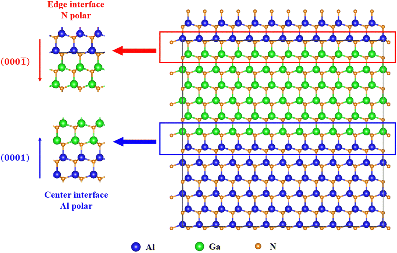
In order to investigate the basal dislocations in GaN grown on AlN, we set up the GaN/AlN (0001) interface supercell as shown in Fig. 1. The lattice constants are set as a = 32.5 Å, b = 3.13 Å and c = 30.11 Å, which are obtained by expanding the lattice constants of AlN (12 × 1 × 6). In this way, we can approximate the compressive stress conditions caused by lattice mismatch during the early growth of GaN on AlN. It is also worth noting that there are two interfaces with different polarities in the interface supercell. Here, we define interface polarity based on the polarity of the AlN part (Al-polarity and N-polarity, Fig. 1). At the center of the supercell, AlN grows along the [0001] direction and the Al atomic layer of AlN is directly connected to GaN at the interface, corresponding to Al-polarity. At the edge of the supercell, AlN grows along the [000![[1 with combining macron]](https://www.rsc.org/images/entities/char_0031_0304.gif) ] direction and the N atomic layer of AlN is directly connected to GaN at the interface, corresponding to N-polarity. This supercell is used to consider the different combinations of basal dislocations at the two polar interfaces.
] direction and the N atomic layer of AlN is directly connected to GaN at the interface, corresponding to N-polarity. This supercell is used to consider the different combinations of basal dislocations at the two polar interfaces.
 | ||
| Fig. 1 Schematic diagram of the GaN/AlN hetero-interface structures with two different polarities in one supercell. | ||
Generally, the dislocations in ideal crystal structures can be described by slipping a plane along a direction.13 In the wurtzite crystal structure, there are four kinds of slip planes: the basal plane (0001), the prismatic plane (100), the pyramidal planes (101) and (11![[2 with combining macron]](https://www.rsc.org/images/entities/char_0032_0304.gif) 2). Then, four slip systems can be constructed: the basal slip system 110 (0001), the prismatic slip system 110 (000), the type-I pyramidal slip system 110 (001) and the type-II pyramidal slip system 113 (112). The basal slip system is the most common one and corresponds to the basal dislocations. The other three slip systems can only appear under appropriate conditions and correspond to threading dislocations, mixed dislocations, and twinning. Therefore, we focus on the basal slip system and construct relevant structures of basal dislocations.
2). Then, four slip systems can be constructed: the basal slip system 110 (0001), the prismatic slip system 110 (000), the type-I pyramidal slip system 110 (001) and the type-II pyramidal slip system 113 (112). The basal slip system is the most common one and corresponds to the basal dislocations. The other three slip systems can only appear under appropriate conditions and correspond to threading dislocations, mixed dislocations, and twinning. Therefore, we focus on the basal slip system and construct relevant structures of basal dislocations.
On the basal plane, the perfect edge dislocations are the 60° dislocations (![[b with combining right harpoon above (vector)]](https://www.rsc.org/images/entities/i_char_0062_20d1.gif) = 1/3 [110], l = [20]), where and l are the Burgers vector and dislocation line, respectively.42 For GaN with the wurtzite structure, there are three kinds of stacking faults associated with three different types of partial dislocations: the intrinsic stacking faults I1 correspond to Frank–Shockley ( = 1/6 [203]) partial dislocations; the intrinsic stacking faults I2 correspond to Shockley partial dislocations ( = 1/3 [100]); the extrinsic stacking faults E correspond to Frank ( = 1/2 [0001]) partial dislocations.43,44 Here we focus on basal dislocations with Burgess vectors and dislocation lines parallel to the basal plane, namely perfect 60° dislocations and Shockley partial dislocations.
= 1/3 [110], l = [20]), where and l are the Burgers vector and dislocation line, respectively.42 For GaN with the wurtzite structure, there are three kinds of stacking faults associated with three different types of partial dislocations: the intrinsic stacking faults I1 correspond to Frank–Shockley ( = 1/6 [203]) partial dislocations; the intrinsic stacking faults I2 correspond to Shockley partial dislocations ( = 1/3 [100]); the extrinsic stacking faults E correspond to Frank ( = 1/2 [0001]) partial dislocations.43,44 Here we focus on basal dislocations with Burgess vectors and dislocation lines parallel to the basal plane, namely perfect 60° dislocations and Shockley partial dislocations.
To construct the basal dislocations at the GaN/AlN interface, we slide some specific Ga and N atoms on the basal planes in GaN. As shown in Fig. 2, there are two different kinds of basal slip planes at the GaN/AlN interface: the glide (the red lines between Ga and N atomic layers) and shuffle (the blue lines between Ga and N atomic layers) slip planes. Since there are two types of polarity GaN/AlN interfaces (Al and N polar interfaces shown in Fig. 1) in the supercell, combining the two polarities can form four types of initial dislocations (Fig. 2). Furthermore, we can construct different combinations of basal dislocations by adjusting the atoms slipping on this basis. To construct the perfect 60° dislocations, we slide half of the GaN atoms on the right along the [110] direction by 1/3[110] length. To construct the Shockley partial dislocations, we first slide half of GaN atoms on the right along the [100] direction by 1/3[100] length, then slide part of these atoms along the [010] direction by 1/3[100] length. In particular, the two Shockley partial dislocations constructed in this way can be regarded as the dissociation of one perfect 60° dislocation. Such dissociation can be viewed as the following reaction:
| = 1/3[110] = 1/3[100] + 1/3[010] = s1 + s2. | (1) |
is the Buggers vector of perfect 60° dislocation, s1 and s2 are the Buggers vectors of two Shockley partial dislocations dissociated from perfect 60° dislocation. By changing the range of the sliding atoms in the second step in building the Shockley partial dislocation, we can adjust the distance between the two Shockley partial dislocations at the GaN/AlN interface.
 | ||
| Fig. 2 Combinations of basal dislocations at the GaN/AlN interface: (a) two glide slip planes, (b) glide slip plane at the Al-polar interface and shuffle slip plane at the N-polar interface, (c) shuffle slip plane at the Al-polar interface and glide slip plane at the N-polar interface, (d) two shuffle slip planes. The red (G) and blue (S) lines indicate glide slip and shuffle slip planes, respectively. | ||
3.2 Formation energies of different dislocation combinations at the GaN/AlN interface
Due to the unique structure of wurtzite GaN and wurtzite AlN, the dislocation combinations formed by atoms sliding on different slip planes are completely different. When atoms slide on a shuffle slip plane (Fig. 2(d)), only the perfect 60° dislocation can be formed at each GaN/AlN interface regardless of the slip method of atoms. The combination of two partial dislocations dissociated from perfect 60° dislocations can only occur when atoms slide on the glide slip plane (Fig. 2(a)). Then the Glide-Shuffle structure shown in Fig. 2(b) includes two Shockley partial dislocations at the Al-polar interface and one perfect 60° dislocation at the N-polar interface. Alternatively, the Shuffle–Glide structure shown in Fig. 2(c) includes one perfect 60° dislocation at the Al-polar interface and two Shockley partial dislocations at the N-polar interface.To study the stability of these dislocations at GaN/AlN interfaces, we need to calculate their formation energies. The formation energy of the dislocation combination (D) can be expressed as:
 | (2) |
| μGa = E(Ga), | (3) |
| μN = E(GaN) − μGa, | (4) |
 | ||
| Fig. 3 Formation energies of basal dislocation combinations at the GaN/AlN interface (DFT calculations). The dislocation distance corresponds to the initial distance between two Shockley partial dislocations at the interface. The dislocation distance of 0 Å corresponds to the perfect 60° dislocations not dissociated into Shockley partial dislocations yet. | ||
The formation energies of dislocations are usually very high, for example, the formation energy of a single threading edge dislocation in GaN is 8–10 eV per cell length.45 Even with such high formation energy, these high energy dislocations could still be formed during the growth of GaN due to the interface strain. In addition, irradiation can induce these high energy dislocations as well, such as the dislocation bands in the low dislocation density region.46 Therefore, our main focus here is not to compare the absolute values of the formation energy of different basal dislocation combinations shown in Fig. 3, but to observe the trend of dislocation formation energy variation with the dislocation distance. The dislocation distance also corresponds to the width of the stacking fault between two Shockley partial dislocations at the interface. From Fig. 3, we can see that by increasing the dislocation distance, the formation energies of the dislocations are almost convergent and a local minimum value can be obtained. Although this is not a strict decomposition and migration path for partial dislocations, it also indicates that the stacking fault width will reach its optimal state when the repulsive effect between Shockley partial dislocations is balanced with the stacking fault energy.
Since the dislocation distance of 0 Å corresponds to the perfect 60° dislocations without dissociating yet, we can further determine whether a perfect 60° dislocation tends to dissociate at different slip planes and polar interfaces. First, after the dissociation of perfect 60° dislocations on the glide basal slip planes, the formation energy is gradually decreased with increasing distance (the black line in Fig. 3). Its formation energy is even lower than that of the perfect 60° dislocation, indicating the stabilization of Shockley partial dislocations on glide slip planes. Moreover, it is interesting to notice that the Glide–Shuffle, Shuffle–Glide dislocation combinations look similar (Fig. 2(b) and (c)), but their formation energies are significantly different (Fig. 3) due to the different interface polarities. The perfect 60° dislocation tends to dissociate into two Shockley partial dislocations at the Al-polar interface (red data points shown in Fig. 3). In contrast, two Shockley partial dislocations at the N-polar interface are only locally stable and tend to recombine (the blue line in Fig. 3). The partial dislocations always have higher formation energies than perfect 60° dislocations (blue data points shown in Fig. 3). This means that the N-polar GaN/AlN interface is more conductive to the formation of perfect 60° dislocations than the Al-polar GaN/AlN interface, while the Al-polar GaN/AlN interface is more conductive to the formation of Shockley partial dislocations than the N-polar GaN/AlN interface.
To further verify the above conclusions at high temperatures during the actual GaN growth process, we performed MD calculations on different dislocation combinations, as shown in Fig. 2 at 300 K and 1300 K and obtained the dislocation formation energies as shown in Fig. 4. We notice the difference of absolute formation energy of these basal dislocations using DFT and MD simulations. Such a difference is due to the different potentials used in MD and DFT. It is well known that the empirical potentials used in MD are not as accurate as those used in DFT. However, such empirical potentials can be used to deal with the properties of materials under realistic situations (including high temperature and large-scale systems), which DFT cannot do anything. The results using the empirical potential simulations usually provide a reasonable trend to understand the physical mechanisms of large scale systems, such as nucleation and growth.36 Since the trend is more important to explore the stability of these basal dislocations and the influence of interface polarity and temperature on dislocations, the empirical potential used in MD is reasonable to study the dislocations at finite temperature.
 | ||
| Fig. 4 Formation energies of basal dislocation combinations at the GaN/AlN interface: (a) MD calculations at 300 K, (b) MD calculations at 1300 K. The dislocation distance corresponds to the initial distance between two Shockley partial dislocations at the interface. The dislocation distance of 0 Å corresponds to the perfect 60° dislocations not dissociated into Shockley partial dislocations yet. | ||
From Fig. 3 and 4(a), we can see that the trends of the formation energy with dislocation distance are similar using DFT and MD-300 K, especially the Glide-Glide dislocation combination (two Shockley partial dislocations at each GaN/AlN interface when dislocation distance is >0 Å). Thus, the empirical potential used in our MD simulations is reasonable to describe the stability trend of these dislocations and is also conducive to further understanding the impact of high temperature on the dislocation behaviors. By comparing Fig. 4(a) and (b), we can find that the most significant difference is that the formation energies of basal dislocation combinations change less with the initial dislocation distance, especially for the Glide-Shuffle and Shuffle–Glide dislocation combinations. This is because the temperature of 1300 K in MD calculations provides atoms with sufficient energy to overcome potential barriers, allowing each dislocation combination to break through the initial dislocation distance limitation and relax to a lower energy structure. Then the dislocation distance shown in Fig. 4(b) only represents the distance between the initial two partial dislocations and does not correspond to the distance between partial dislocations after relaxation. After relaxation, the structures of the four dislocation combinations with different initial dislocation distances at 1300 K are shown in Fig. S9–S12 (ESI†). For example, as shown in Fig. S9 (ESI†), two Shockley partial dislocations remain stable at both two GaN/AlN interfaces and the final distance between the two Shockley partial dislocations (9.381–15.635 Å) becomes similar and larger than the initial dislocation distance (0–15.635 Å). Corresponding to this phenomenon, the formation energies of Shockley partial dislocations (the black line in Fig. 4(b)) become even lower than those of the perfect 60° dislocations on the shuffle slip plane (the purple line in Fig. 4(b)). This once again confirms the stability of Shockley partial dislocations on the glide slip planes, indicating that they may be the most likely basal dislocations to be formed near the GaN/AlN interface. According to the elasticity theory of dislocations, dislocations with smaller Burgers vectors are easier to form. For the Shockley partial dislocations, they correspond to the edge of the intrinsic stacking faults I2 in the wurtzite GaN, and they have the small Burgers vectors. Meanwhile, due to the lattice mismatch between GaN and AlN, the intrinsic stacking faults I2 are easy to form at the GaN/AlN interface. Thus, the Shockley partial dislocations with smaller Burgers vectors are more likely to form on glide slip planes.
In particular, the formation energies of Glide–Shuffle and Shuffle–Glide dislocation combinations remain almost constant with the dislocation distance (the red and blue line in Fig. 4(b)). As shown in Fig. S10 and S11 (ESI†), two Shockley partial dislocations remain stable on the glide slip planes at the Al-polar GaN/AlN interface, while the perfect 60° dislocations (not dissociated into two Shockley partial dislocations) remain stable on the glide slip planes at the N-polar GaN/AlN interface. This once again indicates that the Al-polar GaN/AlN interface is more conductive to the formation of partial Shockley dislocations, while the N-polar GaN/AlN interface exhibits the opposite behavior, supporting the results of DFT calculations. To further understand how the interface polarity affects the generation of basal dislocations, we calculate the charge density of perfect 60° dislocations and Shockley partial dislocations at different polar GaN/AlN interfaces and the results are shown in Fig. S13 and S14 (ESI†), respectively. At the Al-polarized GaN/AlN interface, the structure and charge density exhibit significant distortion near the core of perfect 60° dislocation. However, there is only a relatively small variation in charge density near the two Shockley dislocations. At the N-polarized GaN/AlN interface, the core of perfect 60° dislocations includes Ga atoms. The charge density around N atoms near the dislocation line is almost the same as the charge density around N atoms far away from the perfect 60° dislocation, while the variation of charge density is relatively large near two Shockley partial dislocations. These characteristics of charge density indicate that different polarized GaN/AlN interfaces are conducive to the generation of different favorable basal dislocations.
Overall, the difference between Fig. 3 (DFT calculation results) and Fig. 4 (MD calculation results) is due to the different final stable distances of two Shockley partial dislocations caused by the difference of temperature, but the conclusions are consistent. The trend of dislocation formation energy variation with the dislocation distance, as shown in Fig. 3 and the dislocation formation energies of different dislocation combinations, as shown in Fig. 3 and 4 can indicate the influence of the GaN/AlN interface on basal dislocations.
Although above DFT and MD calculations have presented the effects of basal slip planes and polarities of GaN/AlN interfaces on different combinations of basal dislocations, the investigation of basal dislocation formation at the GaN/AlN interfaces during growth within the supercell framework remains challenging. On the other hand, due to the periodicity of the supercell, different interface polarities and different basal dislocations always coexist in one supercell (Fig. 2). Thus, the influence of a single polar interface on dislocations cannot be directly obtained. Meanwhile, the growth of GaN on AlN in devices usually has only one certain polarity. Therefore, we need to construct a single polar AlN surface for GaN deposition to observe the formation of basal dislocations during actual GaN growth. This helps us to directly understand the influence of interface polarity on the basal dislocations and to understand the dislocations generated during actual GaN growth rather than relying on artificially constructed specific combinations of dislocations. Considering the large number of deposited GaN atoms, we choose MD simulations within the empirical potentials to investigate the early growth of GaN on AlN with different polarities and observe the formation of dislocations.
3.3 Simulation of GaN deposition and growth on AlN
To perform the MD simulations of GaN deposition and growth on AlN, the original hexagonal cell of the AlN substrate is converted into a rectangle shape that can better represent the (110), (100), and (0001) planes in the AlN crystal structure. The cell vectors of the rectangle AlN cell are a = a(1,0,0),  , and c = a(0,0,c/a) (Fig. 5(a)), in which a = b = 3.14 Å, and c = 4.98 Å. To study the growth of GaN, we create a 15 × 15 × 6 supercell as the AlN substrate using the rectangle AlN cell. A total of 4500 Ga atoms and 4500 N atoms are periodically injected towards the AlN substrate from 100 Å height. The initial AlN substrate simulation cell consists of 10
![[thin space (1/6-em)]](https://www.rsc.org/images/entities/char_2009.gif) 800 atoms. These atoms are divided into three groups: Group-1, the atoms in the bottom two AlN layers are fixed during the MD simulations; Group-2, the atoms of top two AlN layers can freely transfer energy with Ga and N atoms that have an initial kinetic energy of 0.17 eV, where the NVE ensemble is used; Group-3, the remaining atoms in the substrate can be used as reservoir to ensure the required substrate temperature for calculation, where the NVT ensemble is used. The structural characteristics of AlN with different polarities are shown in Fig. 5(b). The Al-polar AlN grows along the [0001] directions and the N-polar AlN grows along the [000] direction. In this way, we can simulate the early growth of GaN on two different polar AlN and the corresponding natural generation of dislocations at two different polar GaN/AlN interfaces.
800 atoms. These atoms are divided into three groups: Group-1, the atoms in the bottom two AlN layers are fixed during the MD simulations; Group-2, the atoms of top two AlN layers can freely transfer energy with Ga and N atoms that have an initial kinetic energy of 0.17 eV, where the NVE ensemble is used; Group-3, the remaining atoms in the substrate can be used as reservoir to ensure the required substrate temperature for calculation, where the NVT ensemble is used. The structural characteristics of AlN with different polarities are shown in Fig. 5(b). The Al-polar AlN grows along the [0001] directions and the N-polar AlN grows along the [000] direction. In this way, we can simulate the early growth of GaN on two different polar AlN and the corresponding natural generation of dislocations at two different polar GaN/AlN interfaces.
 | ||
| Fig. 5 (a) The MD simulation box of the AlN substrate. (b) Schematic diagram of AlN structures with two different polarities: Al-polar and N-polar. | ||
3.4 Dislocation in the deposited GaN film on AlN with different polarities
We simulate the growth of GaN at different temperatures (900, 1100, 1300, 1500, 1700, 1900, and 2100 K). The types and the formation progress of dislocations are similar. We then take the growth of GaN at 1700 K as an example to understand its growth progress. Fig. 6 shows the time-resolved progress of dislocations in the deposited GaN film on AlN (Al-polar) at 1700 K. The dislocation types in GaN are identified using a dislocation extraction algorithm (DXA) and the visualization of dislocations is provided by the open visualization tool (OVITO).47,48 Five snapshots during the MD simulation are taken to briefly demonstrate the formation progress of dislocations. It can be seen that the dislocation begins to appear at the GaN/AlN interface at t = 2000 ps as shown in Fig. 6(b) and the GaN film gradually grows and the dislocations increase over time as shown in Fig. 6(c)–(e). Every 2000 ps, 1000 pairs of GaN are deposited, which is approximately two layers of GaN, as shown in the gray areas of Fig. 6.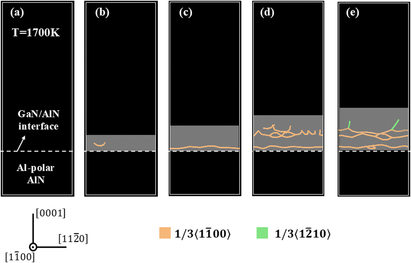 | ||
| Fig. 6 GaN deposition and early growth progress on the Al-polar AlN substrate at 1700 K: (a) t = 0 ps, (b) t = 2000 ps, (c) t = 4000 ps, (d) t = 6000 ps, and (e) t = 8000 ps. The gray areas represent the deposited GaN films. | ||
Only two types of dislocations can be clearly distinguished in the final deposited GaN and their Burgers vectors are b = 1/3100 and b = 1/3110. The b = 1/3100 dislocation is the Shockley partial dislocation, which is the first kind of formed dislocation during GaN growth. The DFT and MD calculations (Fig. 3 and 4) have confirmed that the Shockley partial dislocations can stably exist on the glide slip planes. Thus, the appearance and density increase of Shockley partial dislocations over time are in line with the DFT expectations. Meanwhile, there are no complete independent 60° dislocations during the early growth of GaN, further indicating that Shockley partial dislocations are the main dislocations and do not tend to recombine to form perfect 60° dislocations. Moreover, as shown in Fig. 6(e), the threading edge dislocations (green lines, b = 1/3110) begin to appear in the later stage of GaN deposition and connect directly to the previously formed Shockley partial dislocations (orange lines, b = 1/3100). This indicates that the threading edge dislocations originate from the Shockley partial dislocations during the early growth of GaN, which agrees with the experimental measurements: the formation of threading dislocations in InGaN grown on (0001) GaN is attributed to the Shockley partial dislocations.26 This also means that if we try to reduce the threading edge dislocations and improve GaN-based devices, we may need to pay attention to the early growth of GaN and try to minimize the formation of Shockley partial dislocations.
To consider the effects of different interface polarities, we turn our attention to the N-polar AlN. When the polarity of the AlN substrate changes to N-polar, the time-resolved progress for dislocation (Fig. 7) shows that the formation progress of dislocations is generally similar to that of dislocations in the deposited GaN film on Al-polar AlN substrates. Particularly, the Shockley partial dislocations (b = 1/3100) start appearing at 4000 ps, later than that at the Al-polar interface (2000 ps, Fig. 7(c)). This indicates that the N-polar interface has a certain ability to suppress the formation of the Shockley partial dislocations. This is consistent with the conclusion obtained from DFT and MD calculations mentioned in Section 3.2: the Al-polar GaN/AlN interface is more conductive to the formation of Shockley partial dislocations than the N-polar GaN/AlN interface.
 | ||
| Fig. 7 GaN deposition and early growth progress on the N-polar AlN substrate at 1700 K: (a) t = 0 ps, (b) t = 2000 ps, (c) t = 4000 ps, (d) t = 6000 ps, and (e) t = 8000 ps. The gray areas represent the deposited GaN films. | ||
Then, we further investigate the specific effects of temperature and interface polarity on dislocations. Fig. 8 shows the dislocation density of deposited GaN on AlN with two polarities at different temperatures. Clearly, the Shockley partial dislocations (b = 1/3100) are always the ones with the highest proportion regardless of temperature and the polarity of the AlN substrate. This further indicates that Shockley partial dislocations and the related intrinsic stacking faults I2 are dominant in the early growth of GaN. A small number of threading edge dislocations (b = 1/3110) occur in GaN on the Ga–polar and N-polar AlN substrates, which corresponds to the threading edge dislocations that originate from the Shockley partial dislocations during the early growth of GaN. There are also some dislocations without specific Burgess vectors which are classified as other dislocations in Fig. 8. These dislocations may occur at the junction of GaN with different structures (such as zinc blende and amorphous), and they do not have a specific Burgess vector in the wurtzite structure.
 | ||
| Fig. 8 Temperature effect on the dislocation densities in the deposited GaN film on the AlN substrate with different polarities: (a) Al-polar AlN, (b) N-polar AlN. | ||
Furthermore, the trend of dislocation density varies with temperature in the deposited GaN on AlN substrates with different polarities. For the deposition of GaN on the Al-polar AlN substrate, the Shockley partial density and total dislocation density show a well at 1300 K with increasing temperature. For the deposition of GaN on the N-polar AlN substrate, the dislocation density shows a well at 1900 K with increasing temperature. Thus, in order to minimize the dislocations at the GaN/AlN interface, we can tune temperature, e.g. controlling the growth temperature at 1300 K and 1900 K on the Al-polar and N-polar AlN substrates, respectively. Since dislocations strongly depend on the local geometry distortion around the GaN/AlN interface to investigate the dislocation behavior at different temperatures (Fig. 8), we should take a look at the structural components of the deposited GaN film on the AlN substrate (Fig. 9). Based on the local structure analysis, we notice that the GaN structures during the growth on the AlN substrate include three types: wurtzite, zinc–blende and amorphous. When depositing GaN on AlN with two different polarities at high temperatures (1700–1900 K), the wurtzite structure increases relatively, while the zinc–blende and amorphous structures decrease, which means better crystallinity and fewer dislocations. Additionally, we also observe a peak in the proportion of the zinc blende structure at 1300 K. Correspondingly, the density of other dislocations (undefined Burgess vectors) increases significantly at 1500 K. These characteristics indicate that there is intense competition between wurtzite and zinc blende structure from 1300 to 1500 K and the other dislocations (undefined Burgess vectors) are formed at the junction of these two structures.
 | ||
| Fig. 9 Temperature effect on the structural components in the deposited GaN film on the AlN substrate with different polarities: (a) Al-polar AlN, (b) N-polar AlN. | ||
Additionally, the GaN film deposited on N-polar AlN generally has fewer dislocations (especially Shockley partial dislocations) than on the Al-polar AlN interface. This once again proves the conclusion obtained from DFT calculations: the Al-polar GaN/AlN interface is more conductive to the formation of Shockley partial dislocations than the N-polar GaN/AlN interface. Therefore, choosing N-polar AlN as the substrate and increasing the growth temperature are beneficial for obtaining high-quality GaN layers with fewer dislocations. From the local structure formations (Fig. 9), the deposited GaN on N-polar AlN has a higher proportion of wurtzite structure compared to deposited GaN on Al-polar AlN, which indicates that N-polar AlN is more conducive to the growth of wurtzite GaN that we need.
To further understand how the interface polarity affects the growth of GaN and the generation of dislocations, we calculate the charge density of AlN (Fig. 10). From the structure and charge density of AlN on the (100) plane (the middle panel in Fig. 10), electrons are mainly concentrated near N atoms and the charge density around N atoms at the N-polar AlN surface (N atom terminal) is slightly distorted. Meanwhile, the charge density of AlN on the (000) and (0001) planes intuitively indicates that the charge density of the N polar AlN surface (the left panel in Fig. 10) is higher than that of the Al polar AlN surface (the right panel in Fig. 10), which leads to easier nucleation of GaN on N-polar AlN. Thus, the N-polar AlN surface is more conducive to the growth of wurtzite GaN with fewer dislocations.
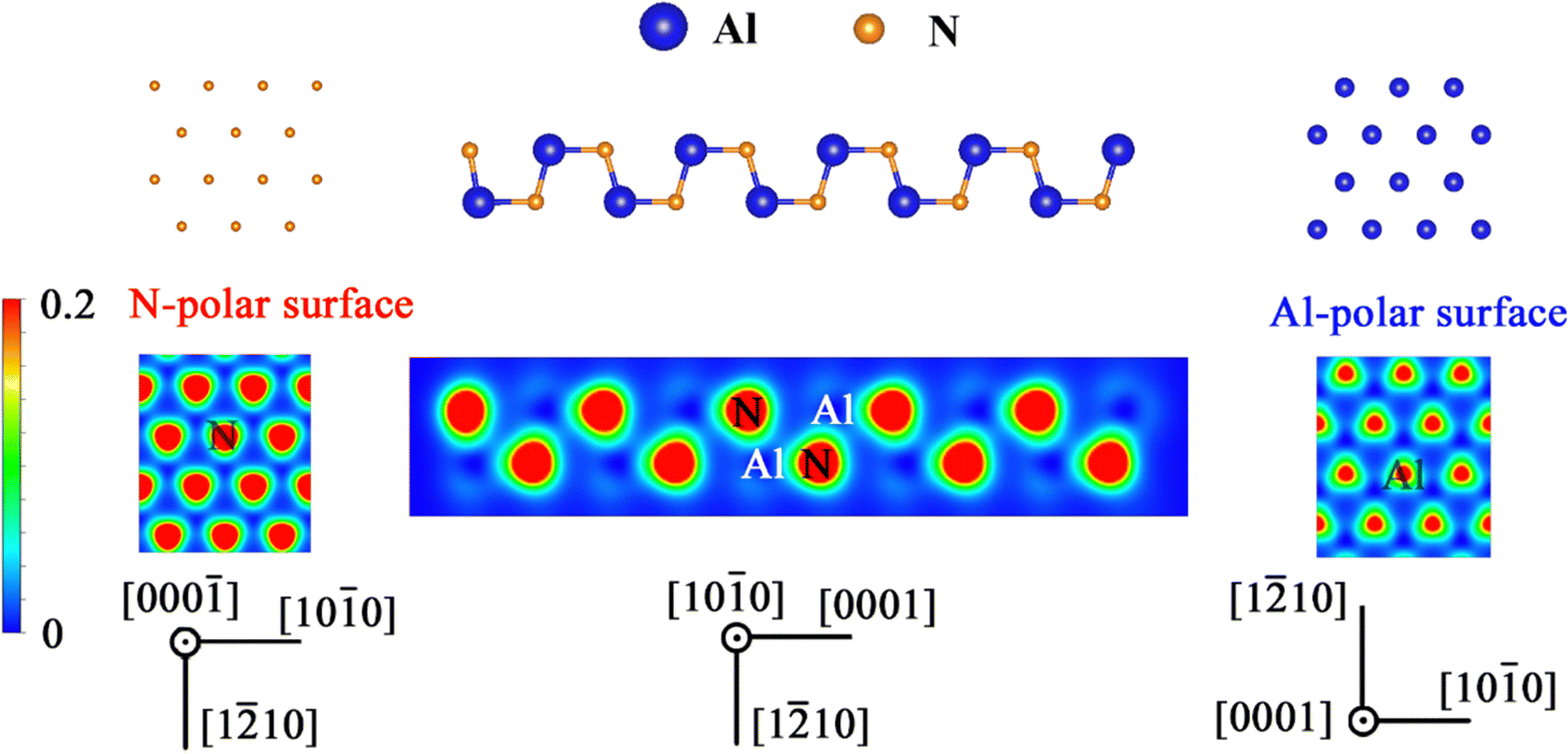 | ||
| Fig. 10 The structure and charge density of AlN on the (000), (100) and (0001) plane. The AlN surfaces at the left and right ends correspond to N polarity and Ga polarity, respectively. | ||
4. Conclusion
We performed DFT calculations and MD simulations to study the behaviors of basal dislocations at the GaN/AlN interface with different polarities. The DFT calculations show that the perfect 60° dislocations and Shockley partial dislocations are favorable at the N-polar GaN/AlN and Al-polar GaN/AlN interfaces, respectively. In addition, the Shockley partial dislocations are thermodynamically stable on glide slip planes at the GaN/AlN interface. Then the MD simulations are used to further study the dislocation formation during the early growth of GaN on the AlN substrate. Clearly, the Shockley partial dislocations are the main dislocations during the early growth of GaN, supporting the results of DFT calculations. Besides, the Shockley partial dislocations are the precursor of the threading edge dislocations, which means that reducing the formation of the Shockley partial dislocations during the early stages of GaN growth can help to reduce the overall dislocation density of GaN in actual GaN-based devices. Moreover, the dislocation density and the proportion of geometry structures in the deposited GaN are investigated at different temperatures and on polar AlN substrates. Overall, the deposited GaN on N-polar AlN has fewer dislocations and a higher proportion of wurtzite structure compared to deposited GaN on Al-polar AlN. Therefore, choosing N-polar AlN as a substrate helps to obtain high-quality GaN with a greater wurtzite structure content and fewer dislocations. By understanding the dislocation behaviors at the GaN/AlN interface and the dislocation formation during the early growth of GaN, our results provide a methodology to improve the GaN growth quality.Data availability
The data that support the findings of this study are available from Dr Yuming Yang (email: ymyang@theory.issp.ac.cn) upon reasonable request.Conflicts of interest
There are no conflicts to declare.Acknowledgements
Y. Z. acknowledges financial support from the “Distinguished Expert of Taishan Scholar” program (No. tstp20221124). X. Z. acknowledges financial support from the National Natural Science Foundation of China (No. 12464034) and the Natural Science Foundation of Ningxia (No. 2024AAC05070). Z. H. acknowledges financial support from the National Natural Science Foundation of Ningxia (No. 2021AAC03241). The super-computing services from the Center for Computational Science of CASHIPS, the ScGrid of Supercomputing Center, Computer Network Information Center of Chinese Academy of Science and AM-HPC are gratefully acknowledged for high-performance computing.References
- S. Zhao, H. P. T. Nguyen, M. G. Kibria and Z. Mi, Prog. Quantum Electron., 2015, 44, 14–68 CrossRef.
- S. DasGupta, M. Sun, A. Armstrong, R. J. Kaplar, M. J. Marinella, J. B. Stanley, S. Atcitty and T. Palacios, IEEE Trans. Electron Devices, 2012, 59, 2115–2122 CAS.
- B. Ozden, M. P. Khanal, S. Youn, V. Mirkhani, K. Yapabandara, M. Park, M. Zhao, H. Liang, P. K. Kandaswamy and Y. Saripalli, ECS J. Solid State Sci. Technol., 2016, 5, P3206 CrossRef CAS.
- F. Roccaforte, P. Fiorenza, G. Greco, R. Lo Nigro, F. Giannazzo, F. Iucolano and M. Saggio, Microelectron. Eng., 2018, 187–188, 66–77 CrossRef CAS.
- K. Grabianska, R. Kucharski, A. Puchalski, T. Sochacki and M. Bockowski, J. Cryst. Grow., 2020, 547, 125804 CrossRef CAS.
- J. K. Hite, T. J. Anderson, L. E. Luna, J. C. Gallagher, M. A. Mastro, J. A. Freitas and C. R. Eddy, J. Cryst. Grow., 2018, 498, 352–356 CrossRef CAS.
- B. Setera and A. Christou, Microelectron. Reliab., 2021, 124, 114336 CrossRef CAS.
- A. Jarndal, L. Arivazhagan and D. Nirmal, Int. J. RF Microw. Comput.-Aided Eng., 2020, 30, e22196 Search PubMed.
- H. Amano, N. Sawaki, I. Akasaki and Y. Toyoda, Appl. Phys. Lett., 1986, 48, 353–355 CrossRef CAS.
- F. A. Ponce, B. S. Krusor, J. S. Major, W. E. Plano and D. F. Welch, Appl. Phys. Lett., 1995, 67, 410–412 CrossRef CAS.
- Y. Li, X. Hu, Y. Song, Z. Su, W. Wang, H. Jia, W. Wang, Y. Jiang and H. Chen, J. Alloys Compd., 2021, 884, 161134 CrossRef CAS.
- K. Wang, M. Li, Z. Yang, J. Wu and T. Yu, CrystEngComm, 2019, 21, 4792–4797 RSC.
- L. Huang, X. Wu, Y. Zou, M. Li and R. Wang, Scr. Mater., 2022, 207, 114276 CrossRef CAS.
- K. Kumakura, T. Makimoto, N. Kobayashi, T. Hashizume, T. Fukui and H. Hasegawa, Appl. Phys. Lett., 2005, 86, 052105 CrossRef.
- C. J. Fall, R. Jones, P. R. Briddon, A. T. Blumenau, T. Frauenheim and M. I. Heggie, Phys. Rev. B:Condens. Matter Mater. Phys., 2002, 65, 245304 CrossRef.
- T. Hamachi, T. Tohei, M. Imanishi, Y. Mori and A. Sakai, Jpn. J. Appl. Phys., 2019, 58, SCCB23 CrossRef CAS.
- R. Wang, X. Tong, J. Xu, C. Dong, Z. Cheng, L. Zhang, S. Zhang, P. Zheng, F.-X. Chen, Y. Zhang and W. Tan, Phys. Rev. Appl., 2020, 14, 024039 CrossRef CAS.
- F. A. Marino, N. Faralli, T. Palacios, D. K. Ferry, S. M. Goodnick and M. Saraniti, IEEE Trans. Electron Devices, 2010, 57, 353–360 CAS.
- S. Besendörfer, E. Meissner, A. Lesnik, J. Friedrich, A. Dadgar and T. Erlbacher, J. Appl. Phys., 2019, 125, 095704 CrossRef.
- L. McCarthy, I. Smorchkova, H. Xing, P. Fini, S. Keller, J. Speck, S. P. DenBaars, M. J. W. Rodwell and U. K. Mishra, Appl. Phys. Lett., 2001, 78, 2235–2237 CrossRef CAS.
- H. Amano, Y. Baines, E. Beam, M. Borga, T. Bouchet, P. R. Chalker, M. Charles, K. J. Chen, N. Chowdhury, R. Chu, C. De Santi, M. M. De Souza, S. Decoutere, L. Di Cioccio, B. Eckardt, T. Egawa, P. Fay, J. J. Freedsman, L. Guido, O. Häberlen, G. Haynes, T. Heckel, D. Hemakumara, P. Houston, J. Hu, M. Hua, Q. Huang, A. Huang, S. Jiang, H. Kawai, D. Kinzer, M. Kuball, A. Kumar, K. B. Lee, X. Li, D. Marcon, M. März, R. McCarthy, G. Meneghesso, M. Meneghini, E. Morvan, A. Nakajima, E. M. S. Narayanan, S. Oliver, T. Palacios, D. Piedra, M. Plissonnier, R. Reddy, M. Sun, I. Thayne, A. Torres, N. Trivellin, V. Unni, M. J. Uren, M. Van Hove, D. J. Wallis, J. Wang, J. Xie, S. Yagi, S. Yang, C. Youtsey, R. Yu, E. Zanoni, S. Zeltner and Y. Zhang, J. Phys. D:Appl. Phys., 2018, 51, 163001 CrossRef.
- T. D. Moustakas, Phys. Status Solidi A, 2013, 210, 169–174 CrossRef CAS.
- I. Belabbas, I. G. Vasileiadis, J. Moneta, J. Smalc-Koziorowska and G. P. Dimitrakopulos, J. Appl. Phys., 2019, 126, 165702 CrossRef.
- R. Li, G. Wu, K. Liang, S. Wang, X. Sun, X. Han, L. Xue, H. Li and S. Liu, Comput. Mater. Sci., 2022, 202, 110991 CrossRef CAS.
- T. Matsubara, K. Sugimoto, N. Okada and K. Tadatomo, Jpn. J. Appl. Phys., 2016, 55, 045501 CrossRef.
- F. Y. Meng, H. McFelea, R. Datta, U. Chowdhury, C. Werkhoven, C. Arena and S. Mahajan, J. Appl. Phys., 2011, 110, 073503 CrossRef.
- X. H. Wu, L. M. Brown, D. Kapolnek, S. Keller, B. Keller, S. P. DenBaars and J. S. Speck, J. Appl. Phys., 1996, 80, 3228–3237 CrossRef CAS.
- F. Tuomisto, K. Saarinen, B. Lucznik, I. Grzegory, H. Teisseyre, T. Suski, S. Porowski, P. R. Hageman and J. Likonen, Appl. Phys. Lett., 2005, 86, 031915 CrossRef.
- J. K. Hite, N. D. Bassim, M. E. Twigg, M. A. Mastro, F. J. Kub and C. R. Eddy, J. Cryst. Grow., 2011, 332, 43–47 CrossRef CAS.
- Y. Chen, J. Liu, K. Liu, J. Si, Y. Ding, L. Li, T. Lv, J. Liu and L. Fu, Mater. Sci. Eng., R, 2019, 138, 60–84 CrossRef.
- Z. Su, Y. Li, H. Yin, Y. Hai, X. Hu, Y. Song, R. Kong, Z. Deng, Z. Ma, C. Du, W. Wang, H. Jia, D. Wang, X. Liu, Y. Jiang and H. Chen, J. Cryst. Grow., 2022, 598, 126867 CrossRef CAS.
- W. Kohn and L. J. Sham, Phys. Rev., 1965, 140, A1133–A1138 CrossRef.
- J. P. Perdew, K. Burke and M. Ernzerhof, Phys. Rev. Lett., 1996, 77, 3865 CrossRef CAS PubMed.
- H. J. Monkhorst and J. D. Pack, Phys. Rev. B, 1976, 13, 5188–5192 CrossRef.
- S. Plimpton, J. Comput. Phys., 1995, 117, 1–19 CrossRef CAS.
- X. W. Zhou, D. A. Murdick, B. Gillespie and H. N. G. Wadley, Phys. Rev. B:Condens. Matter Mater. Phys., 2006, 73, 045337 CrossRef.
- X. W. Zhou, R. E. Jones, C. J. Kimmer, J. C. Duda and P. E. Hopkins, Phys. Rev. B:Condens. Matter Mater. Phys., 2013, 87, 094303 CrossRef.
- X. W. Zhou, R. E. Jones, J. C. Duda and P. E. Hopkins, Phys. Chem. Chem. Phys., 2013, 15, 11078–11087 RSC.
- K. Liang, X. Sun, G. Wu, L. Zhang, S. Liu and Z. Gan, Comput. Mater. Sci., 2020, 173, 109426 CrossRef CAS.
- L. Zhang, H. Yan, G. Zhu, S. Liu, Z. Gan and Z. Zhang, Crystals, 2018, 8, 279 CrossRef.
- H. Li, H. Xiang, H. Huang, Z. Zeng and X. Peng, Ceram. Int., 2020, 46, 11556–11562 CrossRef CAS.
- I. Belabbas, P. Ruterana, J. Chen and G. Nouet, Philos. Mag., 2006, 86, 2241–2269 CrossRef CAS.
- J. P. Hirth, J. Lothe and T. Mura, J. Appl. Mech., 1983, 50, 476–477 CrossRef.
- V. Potin, P. Vermaut, P. Ruterana and G. Nouet, J. Phys.:Condens. Matter, 2000, 12, 10301 CrossRef CAS.
- A. F. Wright and U. Grossner, Appl. Phys. Lett., 1998, 73, 2751–2753 CrossRef CAS.
- S. J. Pearton, R. Deist, F. Ren, L. Liu, A. Y. Polyakov and J. Kim, J. Vac. Sci. Technol., A, 2013, 31, 050801 CrossRef.
- A. Stukowski, V. V. Bulatov and A. Arsenlis, Modell. Simul. Mater. Sci. Eng., 2012, 20, 085007 CrossRef.
- A. Stukowski, Modell. Simul. Mater. Sci. Eng., 2010, 18, 015012 CrossRef.
Footnote |
| † Electronic supplementary information (ESI) available. See DOI: https://doi.org/10.1039/d4cp03069a |
| This journal is © the Owner Societies 2025 |