
High-density Nb:YTaO4 single crystals for X-ray scintillation
Yueshen
Zhou
 *ab,
Dongsheng
Yuan
a,
Encarnación G.
Víllora
a,
Daisuke
Nakauchi
c,
Takumi
Kato
c,
Noriaki
Kawaguchi
c,
Takayuki
Yanagida
c and
Kiyoshi
Shimamura
*ab
*ab,
Dongsheng
Yuan
a,
Encarnación G.
Víllora
a,
Daisuke
Nakauchi
c,
Takumi
Kato
c,
Noriaki
Kawaguchi
c,
Takayuki
Yanagida
c and
Kiyoshi
Shimamura
*ab
aNational Institute for Materials Science, Tsukuba 305-0044, Japan. E-mail: ZHOU.Yueshen@nims.go.jp; SHIMAMURA.Kiyoshi@nims.go.jp
bGraduate School of Advanced Science and Engineering, Waseda University, Shinjuku, Tokyo 169-8555, Japan
cNara Institute of Science and Technology, Takayama-cho, Ikoma, Nara 630-0192, Japan
First published on 27th November 2024
Abstract
Environmental-friendly alternatives to the commercial scintillator CdWO4, which contains the toxic element Cd, are highly desired. As potential candidates, in this work, the scintillation characteristics of Nb:YTaO4 transparent single-crystals grown from melt by the floating-zone technique are studied. It is found that the broad UV luminescence of YTaO4 can be turned into a broad visible one by the partial substitution of Ta with only 2% Nb. Therefore, Nb incorporation promotes a better spectral matching to Si-photodiode detectors while the high stopping power of YTaO4 is kept, being close to that of commercial CdWO4. The scintillation properties of pure YTaO4, with a light yield of 15![[thin space (1/6-em)]](https://www.rsc.org/images/entities/char_2009.gif) 900 ph MeV−1 and an afterglow of 0.008% after 40 ms, are comparable to those of CdWO4. The light yield weighed with a Si-photodiode reaches maximum values for 0.5 & 1% Nb:YTaO4 crystals. An improvement in optical properties is expected by the growth of higher quality crystals by a flux-technique in the future.
900 ph MeV−1 and an afterglow of 0.008% after 40 ms, are comparable to those of CdWO4. The light yield weighed with a Si-photodiode reaches maximum values for 0.5 & 1% Nb:YTaO4 crystals. An improvement in optical properties is expected by the growth of higher quality crystals by a flux-technique in the future.
Introduction
X-ray imaging is very widely used in quotidian medical diagnosis, security inspections, industrial analysis, etc.1,2 The main commercial materials utilized as scintillators for X-ray imaging are Tb or Pr:Gd2O2S (GOS) ceramics, and single crystals of TI:CsI or CdWO4 (CWO) in combination with low-cost Si-photodiodes (Si-PDs). GOS possesses a high light yield (LY) and low afterglow, thus it is mainly used for medical applications. Tl:CsI also exhibits a relatively high LY, but it has a low density and it is hygroscopic.3–7 CWO single crystals are characterized by a high stopping power of 134 × 106 (with the density ρ = 7.9 g cm−3, the effective atomic number Zeff = 64.2, and calculated as ρ × Zeff)4 and low afterglow ∼0.01% after 20 ms,8 allowing rapid luggage/cargo inspection under high energy X-rays while keeping a good dynamic resolution.9–12 Focusing further on CWO, there are a couple of reasons to search for alternative materials: firstly, Cd is a toxic element, secondly the LY depends sensitively on crystal quality (typically varying from 6200 to 28000 ph MeV−1 for brownish to more color-less crystals, respectively),13–15 and thirdly the production cost. In addition, a new scintillator of single-crystal Ce:Gd3(Ga,Al)5O12 (GGAG) is developed for medical applications such as SPECT (Single Photon Emission Computed Tomography) due to its high light yield (35000–55000 ph MeV−1) and short decay time (40–90 ns). However, due to its relatively low stopping power (60 × 106, with ρ = 6.6 g cm−3 and Zeff = 55) and long afterglow (∼4%@1 s), it is not considered a practical alternative to CWO for high-energy X-ray applications.16,17
Tantalum, as an element with a very high atomic number, can form Ta-oxides with a high density. Among potential dense candidates (>7 g cm−3) for scintillation, such as LaTaO4, La3TaO7, Sr4Ta4O15, AlTaO4, GdTaO4, Lu3TaO7, LuTaO4, and YTaO4 (YTO), only the last two have shown a noteworthy LY.18–22 These two rare-earth tantalates are very similar: they have the same crystalline structure (monoclinic fergusonite I2/a) and intrinsic emission by cross-relaxation within the Ta–O complex.23 Though the Lu-tantalate has a stopping power about double of that of YTO, it cannot be grown from melt due to its non-congruent nature.24 Instead, YTO is a congruent melting compound, and a priory presents a higher LY.18,23 The highest value of 15200 ph MeV−1 was reported on a ceramic (here it should be noted that the shown emission spectrum peaks at 420 nm instead of typical 340 nm).18 There is only one report on Bridgman growth of YTO with a LY about half of CWO.25 Other works focus on ceramic synthesis and particularly on the doping with Nb, Pr, and Eu to shift the emission wavelength towards visible to match Si-PD detectors.19,26–28 Despite its congruent nature, the lack of YTO single crystals is due to phase transition. According to the phase diagram, it undergoes tetragonal (I41/a) → monoclinic (I2/a) upon cooling at ∼1450 °C.23 The actual potential of YTO as alternative to CWO is still uncertain.
In this study, transparent Y(Ta1−xNbx)O4 single-crystal sections were obtained from melt-grown boules and characterized in terms of scintillation performance for the first time. YTO and YNbO4 (YNO) form a complete solid solution and emit without the need for activator ions. The evolution of crystalline and optical properties with the composition is analyzed. Aiming at substituting CWO single crystals in X-ray imaging applications, the optimum Nb concentration is elucidated.
Experimental
Crystal growth
Y(Ta1−xNbx)O4 (YTNO) crystals (with x from 0 to 1) were grown by the floating zone (FZ) technique with a four Xe-lamp furnace from Crystal Systems Corp. High-purity raw chemicals, namely Ta2O5 (99.99%), Nb2O5 (99.99%), and Y2O3 (99.99%), were weighed in stoichiometric ratios and mixed. Rods were isostatically pressed at 300 MPa before the sintering at 1500 °C for 10 h in air. Feed and seed rods were counter-rotated at speeds varying between 10–15 rpm, while the growth speed was about 5 mm h−1. The growth was conducted under a constant inert Ar flow of 0.2 L min−1 under atmospheric pressure. The growth under an oxygen-containing atmosphere (air or pure O2) was unpracticable due to the instability of the molten zone. It should be noted that there was no need for seeds since these compounds easily grow as single crystals at high temperatures. On the contrary, they tend to crack upon cooling due to the phase transitions,17 so bulk transparent crystals could be obtained only on some sections of the whole bulk. The growth of pure YTO was particularly difficult, thus only tiny transparent areas could be obtained. Therefore, YTO was grown additionally by the Czochralski (Cz) technique using a 40 kW RF generator. Raw materials were molten in a 5 cm in diameter Ir-crucible, and an Ir-rod was used for seeding. The growth and pulling rates were fixed at 10 rpm and 0.8 mm h−1, respectively, while the growth atmosphere was equally Ar.Characterization
Powder X-ray diffraction (XRD) patterns were recorded using a Rigaku SmartLab3 diffractometer and X-ray rocking curves (XRC) with a PANalytical X'Pert PRO, both with Cu Kα radiation (1.54059 Å). Energy dispersive X-ray (EDX) analysis was performed with a TM3000 Tabletop Scanning Electron Microscope. Optical transmittance was measured using a JASCO UV-vis-NIR spectrometer V-570. Photoluminescence (PL) spectra were acquired with JASCO FP-8600DS fluorescence spectrometer. Homemade setups were employed for the scintillation characterization in terms of X-ray-excited luminescence (XRL), pulsed height spectra (PHS), decay, and afterglow.29–31 The X-ray generator for XRL was operated at 40 kV and 1.2 mA. PHS was conducted using 137Cs 662 keV as excitation source and a photomultiplier tube (PMT, R7600-U200, Hamamatsu) operating at 600 V, with a gain value of 20 and a shaping time of 10 μs, the maximum of the ORTEC570 Shaper. Samples' LY was determined after PHS calibration with a similarly emitting Ce:LGSO single crystal, whose LY of 41000 ph MeV−1 had been calibrated previously using a Si photodiode and a 55Fe 5.9 keV X-ray source. A standard CWO reference purchased from Nihon Kessho Kogaku Co., Ltd (NK&K) was used for the decay and afterglow comparison. The pulse X-ray source for decay measurements was realized by combining an X-ray tube (Hamamatsu N5084) with a laser diode (Hamamatsu PLP-10). The pulse time width was ∼60 ps with a repetition rate of 5 kHz. For the afterglow measurements the same X-ray tube was used in combination with LED (Hamamatsu/470 ± 10 nm). The pulse time width was 2 ms with a repetition rate of 10 Hz. The voltage and tube current supplied for accelerating the photoelectrons to hit a W target were 40 kV and 0.01 mA, respectively.29
Results and discussion
Crystal growth
Fig. 1 shows the images of the YTO crystal grown by the Cz technique and the 0.5% Nb:YTO crystal as an example of FZ growth. For both techniques, transparent single crystals started to grow soon after melting raw materials despite not using single-crystal seeds. Transparent regions were obtained only partially after undergoing phase transition upon fast cooling by switching off the lamps. Nevertheless, as can be seen in the insets of Fig. 1, these are large enough to carry out all the characterizations in transparent single crystals. The Cz-grown YTO crystal was not considered for scintillation characterization due to its yellowish appearance. The origin of this coloration is not clear, but it might be caused e.g. by some ppm level of transition metal contamination from the low-purity ZrO2 ceramics which were used in the form of fine insulating balls around the crucible.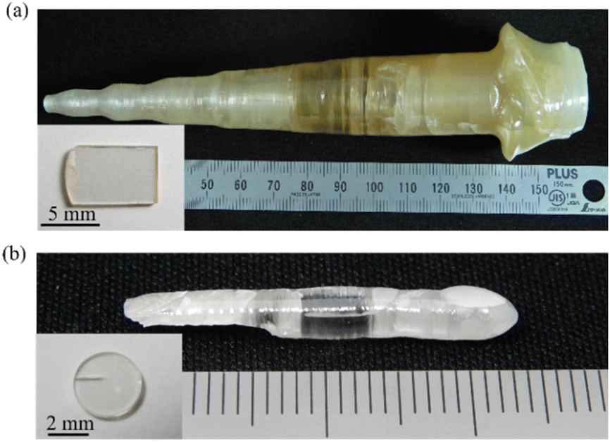 | ||
| Fig. 1 Photographs of (a) Cz-grown YTO and (b) FZ-grown 0.5% Nb:YTO. The insets are photos of corresponding transparent polished plates of 1 mm in thickness. | ||
The substitution of Ta by Nb was evaluated by EDX. As can be seen in Fig. 2, the composition of grown crystals varied in accordance with the nominal content. Therefore, it can be assumed that the segregation coefficient of both cations is equal to 1 in good approximation. This homogeneous incorporation of Nb is important for the relevant scintillation crystals with small Nb concentrations, as will be seen later.
 | ||
| Fig. 2 Nb-content measured by EDX versus nominal concentration. | ||
The nature of the solid-solution between both extreme phases was further investigated by powder XRD, as shown in Fig. 3(a). All the compositions crystallize in the well-known monoclinic fergusonite structure with the space group I2/a. Here, it should be noted that the diffraction peaks −202 and 240 of YTO at ∼47.3 and 47.7 degrees, respectively, gradually shift with the Nb content until they overlap in YNO. The change in lattice parameters was evaluated by refining the XRD patterns with FullProf software, as shown in Fig. 3(b). The largest relative change is found along the c-axis (0.517%), and it is almost double that along the a-axis (0.344%). Along the b-axis the variation is as small as 0.159%. The lattice parameters change almost linearly with the Nb-content in accordance with Vegard's law.32 From this finding, one could expect that the bandgap also changes quasi linearly with the Nb-concentration, as in typical mixed-semiconductors.33 However, it is not the case here, as it will be seen later.
 | ||
| Fig. 3 (a) Powder XRD patterns, (b) lattice parameter change as a function of Nb concentration. | ||
The crystalline quality of transparent crystals was analyzed by XRC measurements in the representative cases of Cz-grown YTO and FZ-grown YNO. The curves of the Cz sample are illustrated in Fig. 4(a) and (b). The Cz-crystal exhibited the narrowest full-width-at-half-maximum (FWHM) of 43′′ for the b-plane sample with the ω-angle varying along the a*. On the same plane but along the perpendicular direction c the FWHM became about double with 88′′. This anisotropy stems from the monoclinic structure and was further analyzed on the c-plane, obtaining an analogous behavior along the a- and b-axes. These results indicate that the crystals anisotropy influences the predominance of crystallographic defects, these being favored along the c- and a-axes for b- and c-planes, respectively. Despite of these anisotropy features, the crystalline quality of Cz-YTO is considered good. In the case of FZ-YNO a similar trend in XRC measurements is found, though the FWHM are larger for the b-plane with 63′′ and 99′′, and worse for the c-plane with multiple peaks and FWHM in the order of 130′′, as shown in Fig. 4(c) and (d). The results illustrate the advantages of the Cz-technique with relatively low temperature-gradients for the growth of high-quality single crystals, particularly in the case of anisotropic monoclinic ones.
 | ||
| Fig. 4 XRC measurements of Cz-grown YTO on (a) b- and (b) c-planes, and FZ-grown YNO on (c) b- and (d) c-planes, with the ω-angle varying along two perpendicular directions. | ||
Optical properties
The transmittance spectra of extreme compounds YTO and YNO are depicted in Fig. 5(a) for non-oriented plates. In the transparent wavelength region, the transmission reaches 75%. Considering that the reflectance has two main contributions, first reflections at the front and rear surfaces, the refractive index of these compounds is roughly estimated to be ∼2.2 (without anisotropy considerations), in good accordance with the values reported for similar tantalates and niobates.34–36 To evaluate the bandgap anisotropy, transmittance measurements were carried out on different planes with light polarization along the three crystallographic axes. The results are summarized in the Tauc plots of Fig. 5(b).37 Within an experimental error of ∼30 meV, caused by the sample alignment and the choice of fitting slope, the bandgap anisotropy of these crystals could not be discerned, in contrast to other anisotropic crystals such as monoclinic β-Ga2O3.38 Consequently, the bandgaps were estimated by averaging the three measured values: 5.00 and 4.40 eV for YTO and YNO, respectively. Assuming that the bandgap anisotropy is also negligible for mixed compositions, the bandgap as a function of Nb-concentration was determined on non-oriented plates, as shown in Fig. 5(c). Contrary to the case of mixed-semiconductors, the bandgap decreases quasi exponentially with the Nb-content from YTO to YNO compositions. The reason is simply that by the Nb incorporation, Nb-4d levels constitute the new conduction band instead of Ta-5d ones, which remain above. This will become evident in the following section about PL measurements. | ||
| Fig. 5 (a) Transmittance spectra of YTO and YNO on non-oriented polished plates of 1 mm in thickness, (b) Tauc plots with polarized light along the three crystallographic axes, and (c) bandgap of YTNO crystals as a function of Nb-concentration. | ||
Excitation and PL spectra of representative samples among the YTNO crystals are illustrated in Fig. 6. The preeminent intrinsic emission of pure YTO and YNO compounds is a broad bright peak (single Gaussians in energy abscissa scale) centered in the UV at 337 nm (3.68 eV) and in the visible at 402 nm (3.08 eV), respectively. Additionally, lower intensity peaks are observed on the high energy side at 273 nm (4.54 eV) and 284 nm (4.37 eV) for YTO and YNO, respectively. Both emission peaks are in good accordance with those reported in ceramics and estimated theoretically: the high- and low-energy emissions are attributed to the radiative recombination of free-excitons (FEs) and self-trapped-excitons (STEs) on Ta/Nb–O complexes, respectively.39–45 Here, it is noteworthy that the YNO FE emission is very close to the bandgap, ∼30 meV below, whereas in the case of YTO it is ∼460 meV. This deviation between both compounds might be related to a large difference in effective masses caused by the extra shell of 32 electrons in Ta. Excitation starts in the UV upon the bandgap (O-2p valence band electrons are excited into the conduction band formed by Ta-5d and Nb-4d orbitals) and increases up to the maxima at 211 and 242 nm for YTO and YNO, respectively. The calculated Stokes-shifts for YTO and YNO are similar, with values of 1.32 and 1.31 eV, respectively. Excitation and PL of mixed crystals did not exhibit a continuous shift in peak maxima but rather a gradual shift in the contribution from Ta–O and Nb–O centers. For 0.5% Nb, the emission from STEs on Ta–O centers still predominated with 60%, while for 2% Nb the emission from STEs on Nb–O ones already reached 83%. These results indicate that free electrons excited into the conduction band and holes in the valence band are much more likely to be trapped on Nb–O complexes than on Ta–O ones due to lower energy levels in the former.46,47 As will be seen in the following, this effect becomes more pronounced when the electrons are excited into higher bands by X-ray irradiation.
 | ||
| Fig. 6 (a) Excitation and (b) emission PL spectra of representative YTNO samples. The emission spectra were excited at the excitation maxima: 211, 210, 216, 224 and 242 nm for 0, 0.5, 1, 2 and 100% Nb, respectively. Correspondingly, the excitation spectra were monitored at the emission maxima: 337, 340, 398, 408, and 402 nm. | ||
Scintillation properties
Upon X-ray excitation, the emission of YTNO crystals exhibits the same features as in PL, except for the absence of the FEs-related high-energy peaks and the difference in emission ratios from Ta–O and Nb–O centers at low Nb-concentrations, as seen in Fig. 7(a) and (b), respectively. On the one hand, the lack of FE emission may be ascribed to FE instability under irradiation according to theoretical estimations.45 The avalanche of secondary high-energy electrons and photons that scatter with the lattice increases the number of phonons, which interact then with FEs to form STEs, thus favoring the formation of STEs instead of FEs.48–50 On the other hand, the predominance of lower energy Nb–O center emission in XRL for the same Nb-content can be attributed to a larger mean-free path of electrons excited in higher energy bands compared to that of those excited into the conduction band in the case of PL.51 In other words, the relaxation path of PL excited electrons is very short, located in the neighborhood of the excited atom or being even interatomic, while X-ray excited electrons can move more freely through the bands, thus increasing the probability of reaching the lowest Nb-4d energy levels. This effect is favorable for scintillators coupled with a standard Si-PD.52 With such a detector, the sensing efficiency of UV emission of YTO is ∼55%, while it rises to 70% for the visible emission of YNO. Therefore, with a Nb concentration as low as 2%, so that the Nb–O center emission in the visible fully dominates the XRL, a maximum detection efficiency can be achieved while largely preserving the high stopping power of YTO (121 × 106, with ρ = 7.57 g cm−3 and Zeff = 63.3, all very close to those of CWO). However, it is necessary to determine also how the LY depends on Nb content. | ||
| Fig. 7 (a) XRL spectra of representative YTNO samples, and (b) comparison between PL and XRL of the Nb–O center emission ratio as a function of the Nb-content. | ||
The LY analysis of YTNO samples was carried out by PHS using a Ce:LGSO reference. Initial PHS measurements on as-grown and annealed YTO suggested that crystals present oxygen vacancies after growth under neutral Ar atmosphere. To suppress these oxygen vacancies, an annealing under air at 1300 °C of 6 h was found to be efficient. As can be seen in Fig. 8(a), the channel number of annealed YTO increased by 76% with respect to the as-grown crystal. The LY depends on the spectral quantum efficiency (QE) of the used PMT (Ultra Bialkali),53 which together with the XRL spectra determines the QE of reference and samples, and the channel number (CN) according to the equation:

 | ||
| Fig. 8 (a) PHS of as-grown, annealed YTO and Ce:LGSO calibrated reference, and (b) relative LY as a function of Nb content. | ||
Consequently, by annealing, the LY of YTO improved notably from 9000 to 15900 ph MeV−1, reaching a value larger than that of CWO benchmark and the highest ever reported.18,25 Subsequently, all YTNO crystals were annealed under the same conditions before the LY measurements. As shown in Fig. 8(b), the LY relative to YTO tends to decrease gradually with the incorporation of Nb till a minimum at 60% Nb, where a sudden increase starts towards YNO. From the practical point of view of the X-ray scintillators in combination with Si-PDs, if we consider again the 2% Nb:YTO crystal, the LY drop relative to YTO from 15900 to 12100 ph MeV−1 (25%) cannot be compensated by the improvement in visible detection efficiency (8400 versus 8770 ph MeV−1 for 2% Nb:YTO and pure YTO, respectively). On the contrary, higher values are estimated for Nb-concentrations ranging from 0.5 to over 1% (9180 and 9200 ph MeV−1, respectively).
At last, the fast decay and afterglow curves of YTNO crystals were measured under pulsed X-rays. The results are summarized in Table 1, while representative curves are depicted in Fig. 9. YTNO crystals are characterized by double exponentials, as well as the reference NK&K CWO (lifetimes of 2.07 and 13.48 μs with 41% and 59%, respectively). In most cases, the faster decay component has a lifetime of <1 μs, while the slower one is in the order of a few μs, ranging between 2 and 8 μs. The origin for the slightly longer τ1 lifetimes of 5 and 10% Nb crystals is not clear and needs further investigation. For all compositions, the contribution of the faster decay predominates, particularly for low Nb concentrations. Most importantly, it should be noted that the decay in YTNO crystals is much quicker than in reference CWO, which can be only meritorious for practical applications. On the other hand, the afterglow of crystals was determined by the remaining percentage at 40 ms after pulsed excitation. Pure YTO and YNO crystals exhibit the lowest afterglow, with 0.008 and 0.016%, respectively. These values are rather low, particularly the one of YTO is comparable to that of reference NK&K CWO. In contrast, mixed crystals exhibited a higher afterglow, mostly in the order of 0.2–0.3%, suggesting the presence of a larger concentration of defects that act as traps.
| Compounds | Light yield (ph MeV−1) | Decay time [μs] | Afterglow [@40 ms%] | |
|---|---|---|---|---|
| τ 1 | τ 2 | |||
| YTaO4 | 15900 |
0.52 (55%) | 1.90 (45%) | 0.008% |
| 0.5% Nb | 13900 |
0.78 (71%) | 5.54 (29%) | 0.310% |
| 1% Nb | 13500 |
0.87 (71%) | 6.16 (29%) | 0.210% |
| 2% Nb | 12100 |
0.82 (63%) | 6.15 (37%) | 0.710% |
| 5% Nb | 11500 |
1.54 (65%) | 7.91 (35%) | 0.230% |
| 10% Nb | 12200 |
1.22 (62%) | 6.55 (38%) | 0.180% |
| 20% Nb | 11900 |
0.56 (59%) | 5.13 (41%) | 0.020% |
| 40% Nb | 10300 |
0.61 (58%) | 5.21 (42%) | 0.019% |
| 60% Nb | 9600 | 0.56 (61%) | 5.04 (39%) | 0.041% |
| 80% Nb | 12500 |
0.51 (60%) | 5.12 (40%) | 0.020% |
| YNbO4 | 14300 |
0.47 (55%) | 3.62 (45%) | 0.016% |
| CdWO4 (N&KK) | 14000 |
2.07 (41%) | 13.48 (59%) | 0.006% |
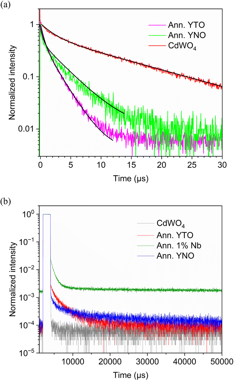 | ||
| Fig. 9 (a) Decay curves of representative annealed YTO, YNO, and reference NK&K CWO, and (b) afterglow curves of the same three crystals and the additional 1% Nb:YTO one. | ||
Conclusions
In conclusion, current work demonstrates the potential of environmental-friendly Nb:YTO single crystals as an alternative to commercial CWO single crystal scintillator, which contains toxic Cd. In contrast to properties measured on ceramic samples, the scintillation properties of YTNO transparent single crystals (grown by the FZ technique) are determined for the first time. YTO single crystal possesses a single broad UV emission upon X-ray excitation and exhibits the best scintillation properties, with a record LY of 15900 ph MeV−1 and an afterglow as low as 0.008% after 40 ms, both comparable to benchmark CWO. Instead, for mixed crystals two intrinsic broad peaks are observed in the UV and visible wavelength regions and are associated with Ta–O and Nb–O emission centers, respectively. With a Nb-concentration as low as 2%, most of the emission takes place at the Nb–O center. Therefore, better spectral matching to Si-PDs can be achieved while maintaining the high stopping power of YTO. However, as the LY tends to decrease with the Nb incorporation, the maximum total performance of the scintillator & Si-PD unit is found for 0.5 & 1% Nb:YTO single crystals. In the end, however, the optimum Nb concentration depends on crystal perfection and impurities. It is found that the crystalline quality of a Cz-grown YTO single crystal is notably higher than that of FZ-grown crystals. Therefore, significant improvements in LY and afterglow can be envisaged for higher-quality Nb:YTO crystals in the future. In any case, as these compounds undergo phase transition upon cooling from the molten state, it is still necessary to find a proper flux-growth method for the synthesis of large-size single crystals at lower temperatures below the phase transition. PbO, PbF2 and mixtures of them are the most typically employed fluxes for the growth of oxides at lower temperatures. We prioritize, however, the use of non-toxic materials for the growth so that the whole production process can be environmentally friendly. Other compounds such as B2O3, Bi2O3, V2O5, BaCl2, Na2CO3, etc., are under consideration. Furthermore, the flux growth under high pressure is another promising alternative. Such hydrothermal growth requires investigating a proper mineralizer, thermal gradients, and pressure, which is time-consuming, but instead, it offers the largest scalability potential.
Data availability
The data used to support the findings of this study are included within the article.Conflicts of interest
There are no conflicts to declare.Acknowledgements
The authors would like to sincerely thank Mr. Satoshi Yamamoto for his kind support with crystal polishing. This work was supported by “Advanced Research Infrastructure for Materials and Nanotechnology in Japan (ARIM)” of the Ministry of Education, Culture, Sports, Science and Technology (MEXT). Proposal Number JPMXP1223NM5337.References
- C. W. E. Eijk, Phys. Med. Biol., 2002, 47, R85–R106 CrossRef PubMed.
- D. Yuan, F. Moretti, D. Perrodin, G. Bizarri, T. Shalapska, C. Dujardin and E. Bourret, CrystEngComm, 2022, 22, 3497–3504 RSC.
- C. M. Michail, G. P. Fountos, S. L. David, I. G. Valais, A. E. Toutountzis, N. E. Kalyvas, I. S. Kandarakis and G. S. Panayiotakis, Meas. Sci. Technol., 2009, 20, 104008 CrossRef.
- Y. K. Kim, H. K. Kim, G. Cho and D. K. Kim, Nucl. Instrum. Methods Phys. Res., Sect. B, 2004, 225, 392–396 CrossRef CAS.
- W. Wang and T. Li, Int. J. Appl. Ceram. Technol., 2015, 12, E249–E255 CAS.
- V. V. Postupaev, Nucl. Instrum. Methods Phys. Res., Sect. A, 2019, 923, 147–156 CrossRef CAS.
- E. E. Ovechkina, V. Gaysinskiy, S. R. Miller, C. Brecher, A. Lempicki and V. V. Nagarkar, Radiat. Meas., 2007, 42, 541–544 CrossRef CAS PubMed.
- NK&K Crystals, Cadmium Tungstate, available online: https://nkk.co.jp/en/products/scintillator/scintillator/ (accessed August 8, 2024).
- L. Bardellia, M. Binia and P. G. Bizzetia, et al. , Nucl. Instrum. Methods Phys. Res., Sect. A, 2006, 569, 743–753 CrossRef.
- K. Ichiba, T. Kato, K. Watanabe, Y. Takebuchi, D. Nakauchi, N. Kawaguchi and T. Yanagida, J. Lumin., 2024, 266, 120327 CrossRef CAS.
- D. Yuan, E. Víllora, N. Kawaguchi, D. Nakauchi, T. Kato, T. Yanagida and K. Shimamura, Appl. Phys. Express, 2022, 15, 022010 CrossRef.
- D. Yuan, E. Víllora, N. Kawaguchi, D. Nakauchi, T. Kato, T. Yanagida and K. Shimamura, Jpn. J. Appl. Phys., 2023, 62, 010614 CrossRef CAS.
- G. Saatsakis, D. Linardatos, K. Ninos, I. Valais, N. Kalyvas, A. Bakas, I. Kandarakis, G. Fountos, G. Panayiotakis and C. Michail, Procedia Struct. Integr., 2020, 28, 971–977 CrossRef.
- Advatech UK, Radiation Detectors and Sensors, available online: https://www.advatech-uk.co.uk/cdwo4.html (accessed August 8, 2024).
- C. Michail, V. Koukou, N. Martini, G. Saatsakis, N. Kalyvas, A. Bakas, I. Kandarakis, G. Fountos, G. Panayiotakis and I. Valais, Crystals, 2020, 10, 429 CrossRef CAS.
- Epic Crystal, GAGG(Ce) Crystal, available online: https://www.epic-crystal.com/scintillation-crystals/gaggce-crystal.html (accessed August 8, 2024).
- M. Yoneyama, J. Kataoka, M. Arimoto, T. Masuda, M. Yoshino, K. Kamada, A. Yoshikawa, H. Sato and Y. Usuki, J. Instrum., 2018, 13, P02023 CrossRef.
- E. D. Bourret, D. M. Smiadak, R. B. Borade, Y. Ma, G. Bizarri, M. J. Weber and S. E. Derenzo, J. Lumin., 2018, 202, 332–338 CrossRef CAS.
- O. Voloshyna, S. V. Neicheva, N. G. Starzhinskiy, I. M. Zenya, S. S. Gridin, V. N. Baumer and O. Ts. Sidletskiy, Mater. Sci. Eng., B, 2013, 178, 1491–1496 CrossRef CAS.
- H. Yang, F. Peng, Q. Zhang, C. Guo, C. Shi, W. Liu, G. Sun, Y. Zhao, D. Zhang, D. Sun, S. Yin, M. Gu and R. Mao, CrystEngComm, 2014, 16, 2480–2484 RSC.
- D. Nakauchi, T. Kato, N. Kawaguchi and T. Yanagida, Radiat. Phys. Chem., 2021, 182, 109390 CrossRef CAS.
- X. Liu, S. Chen, M. Gu, M. Wu, Z. Qiu, B. Liu, C. Ni and S. Huang, Opt. Mater. Express, 2014, 4, 172–178 CrossRef.
- M. Lepple, S. V. Ushakov, K. Lilova, C. A. Macauley, A. N. Fernandez, C. G. Levi and A. Navrotsky, J. Eur. Ceram. Soc., 2021, 41, 1629–1638 CrossRef CAS.
- X. Xing, X. Wang, Q. Zhang, G. Sun, C. Shi, W. Liu, D. Sun and S. Yin, J. Am. Ceram. Soc., 2016, 99, 1042–1046 CrossRef CAS.
- L. I. Kazakova, A. B. Dubovsky, G. V. Semenkovich and O. A. Ivanova, Radiat. Meas., 1995, 24, 359–360 CrossRef CAS.
- P. Magnan, Nucl. Instrum. Methods Phys. Res., Sect. A, 2003, 504, 199–212 CrossRef CAS.
- T. Yanagida, Proc. Jpn. Acad., Ser. B, 2018, 94, 75–97 CrossRef CAS PubMed.
- O. V. Voloshyna, I. A. Boiaryntseva, V. N. Baumer, A. I. Ivanov, M. V. Korjik and O. Ts. Sidletskiy, Nucl. Instrum. Methods Phys. Res., Sect. A, 2014, 764, 227–231 CrossRef CAS.
- T. Yanagida, Y. Fujimoto, T. Ito, K. Uchiyama and K. Mori, Appl. Phys. Express, 2014, 7, 062401 CrossRef CAS.
- T. Yanagida, M. Koshimizu, G. Okada, T. Kojima, J. Osada and N. Kawaguchi, Opt. Mater., 2016, 61, 119–124 CrossRef CAS.
- T. Yanagida, G. Okada, T. Kato, D. Nakauchi and S. Yanagida, Appl. Phys. Express, 2016, 9, 042601 CrossRef.
- A. R. Denton and N. W. Ashcroft, Phys. Rev. A: At., Mol., Opt. Phys., 1991, 43, 3163–3164 CrossRef PubMed.
- S. Lee, R. Levi, W. Qu, S. Lee and C. Randall, J. Appl. Phys., 2010, 107, 023523 CrossRef.
- B. Gong, D. Shen, G. Ren, H. Zhang and Z. Yin, J. Cryst. Growth, 2002, 235, 320–326 CrossRef CAS.
- M. Higuchi, K. Ando, J. Takahashi and K. Kodaira, J. Ceram. Soc. Jpn., 1993, 101, 118–120 CrossRef CAS.
- X. Wang, H. Yang, G. Zhang, Q. Zhang, R. Dou, S. Ding, J. Luo, W. Liu, G. Sun and D. Sun, Acta Phys. Sin., 2016, 65, 087801 CrossRef.
- Y. Zhou, D. Yuan, N. Kawaguchi, D. Nakauchi, T. Kato, T. Yanagida and K. Shimamura, J. Cryst. Growth, 2023, 624, 127432 CrossRef CAS.
- W. Mu, X. Chen, G. He, Z. Jia, J. Ye, B. Fu, J. Zhang, S. Ding and X. Tao, Appl. Surf. Sci., 2020, 527, 146648 CrossRef CAS.
- M. Bharathy, V. A. Rassolov, S. Park and H. C. Loye, Inorg. Chem., 2008, 47, 9941–9945 CrossRef CAS PubMed.
- L. Qin, D. Wei, Y. Huang, S. I. Kim, Y. M. Yu and H. J. Seo, Inorg. Chem., 2013, 52, 10407–10413 CrossRef CAS PubMed.
- M. Bharathy, V. A. Rassolov and H. C. Loye, Chem. Mater., 2008, 20, 2268–2273 CrossRef CAS.
- Z. Feng, B. Lou, Q. Chen, M. Yin, C. Ma and C. Duan, Inorg. Chem., 2021, 60, 16614–16625 CrossRef CAS.
- C. Chen, Y. Lin, P. Lai, H. Lin, G. Tan, H. Lin and R. Schaller, Adv. Opt. Mater., 2022, 10, 2200005 CrossRef CAS.
- B. Chen, R. Chen and B. Huang, Adv. Energy Sustainability Res., 2023, 4, 2300018 CrossRef CAS.
- Q. Guo, X. Zhao, B. Song, J. Luo and J. Tang, Adv. Mater., 2022, 34, 2201008 CrossRef CAS.
- Q. Zheng, F. Wu, L. Chen, F. Qian, K. Yang, Z. Ge, P. Song and J. Feng, Mater. Lett., 2020, 268, 127586 CrossRef CAS.
- X. Liu, Y. Li, T. Liang, W. Liu and J. Fan, J. Phys. Chem. Lett., 2022, 13, 1373–1381 CrossRef CAS.
- Z. Tan, J. Pang, G. Niu, J. Yuan, K. Xue, X. Miao, W. Tao, H. Zhu, Z. Li, H. Zhao, X. Du and J. Tang, Nanophotonics., 2021, 10, 2249–2256 CrossRef CAS.
- V. Kumar and Z. Luo, Photonics, 2021, 8, 71 CrossRef CAS.
- Y. Qin, Z. Li, F. Gao, H. Chen, X. Li, B. Xu, Q. Li, X. Jiang, W. Li, X. Wu, Z. Quan, L. Ye, Y. Zhang, Z. Lin, L. Pedesseau, J. Even, P. Lu and X. Bu, Adv. Mater., 2022, 34, 2201666 CrossRef CAS.
- Q. Zheng, F. Wu, L. Chen, F. Qian, K. Yang, Z. Ge, P. Song and J. Feng, Mater. Lett., 2020, 268, 127586 CrossRef CAS.
- T. Yanagida, Opt. Mater., 2013, 35, 1987–1992 CrossRef CAS.
- K. Nakamura, Y. Hamana, Y. Ishigami and T. Matsui, Nucl. Instrum. Methods Phys. Res., Sect. A, 2010, 623, 276–278 CrossRef CAS.
| This journal is © The Royal Society of Chemistry 2025 |