DOI:
10.1039/D4YA00183D
(Paper)
Energy Adv., 2024,
3, 1389-1400
Excellent field emission with enhanced photodetection behavior of multiwalled carbon nanotubes: experimental and theoretical study
Received
20th March 2024
, Accepted 1st May 2024
First published on 1st May 2024
Abstract
In this study, we synthesized multiwalled carbon nanotubes (MWCNTs) using the direct liquid injection chemical vapor deposition (DLICVD) method, the growth temperatures were varied to investigate their unique properties. To fully characterize these MWCNTs, we examined their surface morphology utilizing scanning electron microscopy (SEM). Additionally, we used UV-visible spectroscopy to evaluate their energy band gap, which provided insight into their electrical characteristics. The most remarkable results of our study were the impressive field emission properties of the MWCNTs. Specifically, they exhibited an extraordinarily low emission threshold field of approximately 0.1 V μm−1, showcasing their potential for advanced electron emission applications. In addition, these MWCNTs demonstrated a remarkably high current density of roughly 1 mA cm−2, which emphasized their superior electrical conductivity. Expanding the scope of our investigation, we integrated MWCNT-based thin films into photodetector devices, which opened up exciting possibilities in optoelectronics. Under an illumination intensity of 25 mW cm−2, these devices exhibited a maximum responsivity of 1.031 A W−1, illustrating their sensitivity to incoming light. Furthermore, our research highlights the excellent detectivity of these MWCNT-based photodetectors, measuring an impressive 2.178 × 10¹⁰ jones under the same illumination conditions. The remarkable performance of the MWCNT-based photodetector device extended to its external quantum efficiency, which reached an astonishing 174.9%.
1. Introduction
We are living in an energy crisis era. Energy generation is an expensive process and this will aid in energy storage if we save the produced electricity. Significant amounts of energy production are leveraging the rising demand for electronic devices with display and current cold emitters. Carbon-based field emitters have been investigated extensively to give better field emission devices.1–5 Carbon nanotubes (CNTs)6 have exceptional physical, chemical, mechanical and structural properties, and they are the perfect quantum system for exploring the one-dimensional physics and applications in nanoscale devices. The CNT growth7 can be achieved by using many different methods such as arc discharge, laser ablation and chemical vapor deposition methods, but the chemical vapor deposition is the best way to synthesize high purity and high yield carbon nanotubes.8,9 The CNTs are also employed in many electrical devices because of their one-dimensional growth, high aspect ratio, and distinctive structural characteristics, which have gained international interest.8–11 Low-energy argon (Ar) ion irradiation of multi-walled carbon nanotubes (MWCNTs) was investigated by Sharma et al. with 1.2 keV ions at fluences ranging from 5 × 10¹⁵ to 1.6 × 10¹⁷ ions per cm2.12 Structural changes were determined using Raman spectroscopy. The irradiation improved the field-emission, with lower turn-on and threshold fields of 1.3 and 3.2 V μm−1, respectively, and a higher field enhancement factor (β) of 9469, which were promising for practical applications. A variety of catalysts such as: Ag, Au, Fe, Mg and Mo were used for the CNT growth but the best nanotube growth was found by using transition metal catalysts such as: Co, Fe, and Ni. The benefits of such a catalyst are that they can be easily removed from the process of distillation.4,13,14 Compared to thin films formed with low electrical conductivity and optical transparency, metal oxides and other nanomaterials, the thin films based on carbon nanotubes exhibit good electrical conductivity and great optical transparency, indicating their suitability for use in electronic applications.15,16 These are also used in a large number of devices due to the extraordinary and attractive properties of the CNTs and these are often substituted for of indium tin oxide (ITO) glass.
The CNTs have been thoroughly studied for use in field emission displays (FEDs) and as electron microscopy probes because of their low threshold voltage, strong emission current, distinctive structure, and chemical stability. In additionally, they are utilized in the single-electron transistor (SET) probe and the field-effect transistor (FET).17 The field emission properties of both single-walled carbon nanotubes (SWCNTs) and multi-walled carbon nanotubes (MWCNTs) were investigated and the high field emission property of the MWCNTs was also investigated.18–27 The MWCNTs synthesized at elevated temperatures via thermal CVD require a catalyst for tube growth, making it challenging to extract the catalyst from the tubes. To address this issue, we have employed a transition metal that readily dissolves in organic solvents.28–32 A type of transition metal which is easily dissolved in organic solvents, was used to resolve these problems.
The quantum dots, quantum wells, carbon nanotubes and graphene exhibit unique properties and have a wide range of photodetection from the ultraviolet to the THz.33,34 Since the atomic structure of the MWCNT may be determined by visualizing graphene sheets that have been rolled to create a cylinder, the MWCNT is utilized in this research for the creation of photodetectors. When compared to graphene, the optical characteristics of CNTs vary significantly due to their one-dimensional existence. Each sub-band in a CNT has a unique angular momentum, and as a result, an optical transfer selection law exists. This is the first significant distinction. Saini et al. synthesized vertically aligned multiwalled carbon nanotubes (MWCNTs) and bi-metal (Cu and In) decorated CNTs and the In–Cu–MWCNTs demonstrated a notable increase in current density to 7.46 mA cm−2 when compared to the 2.83 mA cm−2 of pristine CNTs.35 For example, regarding the CNT axis, the optical absorption can be maximized or suppressed depending on the direction of polarization. The second distinction worth noting results from the quasi-one-dimensional material's heightened Coulomb interaction, which causes a large exciton binding energy that is predominant in the visible, near, and mid-infrared optical absorption in CNTs. It has major implications for photodetectors because there must be sufficiently large electric fields to dissociate the exciton in the photoconductive devices.
In this investigation, we have synthesized the MWCNTs using a direct liquid injection thermal CVD method, using a Co catalyst under controlled conditions at different temperatures.36–38 Centrifugation and repeated washing cycles were used for the filtration. An ultrahigh vacuum is usually needed to test the nanomaterials’ field emission properties. Another outcome of the present research is that we used a rotary vacuum system to investigate the field emission properties of the MWCNTs, which reduces the cost of manufacturing devices based on those nanomaterials. In this research article we have discussed have remarkable field emission features of the MWCNTs, highlighting their viability for electron emission applications with an ultra-low emission threshold field and high current density. The utilization of MWCNT-based thin films as photodetectors, which exhibit remarkable responsiveness, detectivity, and quantum efficiency together with an amazing linear dynamic range, which highlights their prospects for use in cutting-edge photodetector technology. These results are a complete investigation of MWCNTs, from novel production to a wide range of application possibilities, with each component contributing to a thorough knowledge of these nanomaterials. One of the remarkable characteristics of these MWCNTs is their exceptional field emission performance. The field emission properties indicate an ultra-low emission threshold field of approximately 0.1 V μm−1, coupled with a high current density of around 1 mA cm−2. These findings suggest that MWCNTs hold great promise for field emission applications. Furthermore, the MWCNTs were integrated into a thin film to create a photodetector device. This MWCNT-based photodetector exhibited outstanding optical properties. The maximum responsivity reached an impressive value of 1.0 A W−1, accompanied by a remarkable detectivity of 2.1 × 10¹⁰ jones under an illumination intensity of 25 mW cm−2. Moreover, the external quantum efficiency (EQE) of this MWCNT-based photodetector reached an extraordinary 174.9%, indicating its high sensitivity to incident light. Notably, it also demonstrated an exceptional linear dynamic range of 18.4 dB at an illumination intensity of 100 mW cm−2.
2. Experimental techniques
2.1 Synthesis of multiwall carbon nanotubes
The MWCNTs were synthesized by using a catalytic growth direct liquid injection chemical vapour deposition technique.7,39 In this method, ethanol was used as a carbon source and the catalyst was Co nanoparticles. The Co catalyst was prepared by a co-precipitation method. These nanoparticle catalysts create some nucleation points and the carbon nanotubes were grown on these nucleation points.40,41 The growth of the carbon nanotubes was performed at two different temperatures (650 °C and 750 °C) and used them in field emission devices and photodetectors. The reaction inside the chamber is been given by eqn (1) and (2).| | 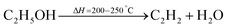 | (1) |
| |  | (2) |
2.2 Purification of the nanotubes
It was important to purify the nanotubes in order to get pure and defect-free nanotubes for the Raman spectroscopy analysis because in both methods, the synthesised nanotubes at 750 °C and 650 °C retained part of the Co catalyst inside the nanotube. The synthesised nanotube was placed in a nitric acid solution during the purification procedure and agitated for 12 h. After centrifugation and washing with deionized water, the pure nanotubes made from the dissolved Co nanoparticles in nitric acid were produced. The following is the reaction that purifies the nanotubes:| | | CnHn(Co) + HNO3 → CnHn(nanotube) + Co(NO3)2 + NO + H2O | (3) |
2.3 Device fabrication
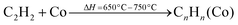
In an in-house built device using the Keithley Electrometer (model 6517 B), field emission measurements at a base pressure of ∼1 × 10⁻² torr using a rotary pump were performed. A schematic representation of the experimental set-up used for field emission analysis is shown in Fig. 1.3,5 The field was applied between two electrodes and the electrons were released from the cathode, traveling towards the anode.
 |
| | Fig. 1 The schematic representation of the field emission set-up. | |
3. Material characterizations
3.1 Scanning electron microscopy analysis
Using field emission scanning electron microscopy (Jeol JSM-7610F), at 100 nm, the morphology and microscopic structure of prepared carbon nanotubes were obtained. Fig. 2 shows the SEM image of the MWCNTs grown at different temperatures on the Co catalyst. Due to the MWCNTs substrate-free catalytic growth, the random orientation of the tubes can be seen on each grain. Micrographs were taken and magnified at the same scale. The amount of MWCNTs that were produced at 650 °C and 750 °C is shown in Fig. 2(a) and (b), respectively. At 650 °C, the lower molecules were broken down to produce fewer atoms and have fewer nucleation points, but at 750 °C, the higher molecules were broken down and their nucleation points increased, resulting in the formation of more MWCNT clusters. Since the density of MWCNTs grown at 750 °C was higher than that of the MWCNTs grown at 650 °C it offers a greater surface current and a higher area for tunneling electrons, making them suitable for use in field emitter applications.
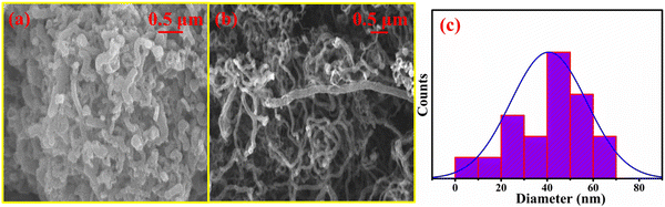 |
| | Fig. 2 (a) and (b) The SEM images of the MWCNTs grown at 650 °C and 750 °C, (c) the average diameters. | |
3.2 TEM analysis
The MWCNTs, synthesized by using the DLICVD method, were analyzed by a tunneling electron microscope (Tecnai™ G2 20). Fig. 3(a) shows the tubular structure of the nanotube together with a hollow space inside the tube. Fig. 3(b) shows the multiple carbon layers formed in the nanotube. The inner and outer diameter of the nanotube was found to be 14 nm and 23 nm, respectively. The TEM images of MWCNTs clearly reveal the multiwall growth of the carbon nanotubes. The tubular and layered walls of the CNTs efficiently contribute to the current enhancement as well as the active sensing sites.
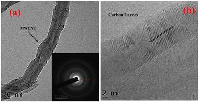 |
| | Fig. 3 The TEM of the MWCNTs at (a) 20 nm and (b) 2 nm scale. | |
3.3 UV-visible spectroscopy analysis
A UV visible spectrophotometer (ThermoScientific Evolution 202) was used to record the UV-visible absorbance spectra of the multiwall carbon nanotube synthesized at different temperatures and the results are plotted in Fig. 4. Energies near to the bandgap gave a sharp increase in absorption, which presents itself as an absorption edge in the UV visible absorption spectra.42 The optical bandgap of the synthesized nanotube was calculated using the Tauc relationship in eqn (4):| |  | (4) |
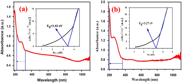 |
| | Fig. 4 The UV analysis results for the MWCNT synthesized at (a) 650 °C and (b) 750 °C. | |
The MWCNT absorption peak occurs at 249 nm, which can be due to π to π* transition from the density of states.43 The redshift of the sample prepared at 650 °C is higher than that of the sample prepared at 750 °C as seen in the Fig. 4, which shows that the quantum confinement of the nanotube was amplified by increasing the growth temperature. The lower bandgap of the MWCNT can be of benefit to the higher field emission property.
3.4 XRD analysis
The XRD patterns of MWCNTs were obtained by using an X-ray diffractometer (Philips PANanalytical X’Pert PRO) and are shown in Fig. 5. The XRD results confirmed the crystalline nature of MWCNTs and the peak indexing (002), (100), (101) represents the hexagonal structure.44 The presence of the (002) peak in the XRD suggested that carbon nanotubes are multi-walled. The crystallite size of the synthesized MWCNT at 650 °C and 750 °C were calculated by the Debye–Scherrer formula and found to be 14 nm and 16 nm, respectively.
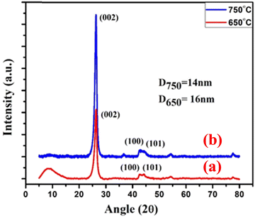 |
| | Fig. 5 The XRD analysis of the MWCNTs synthesized at (a) 650 °C and (b) 750 °C. | |
3.5 Dynamic light scattering (DLS) analysis
The particle sizes of the MWCNTs were obtained using a nano zetasizer (Malvern PANalytical Nano NZS90), in which the particle size was determined from the colloidal particle Brownian motion and this is shown in Fig. 6. To analyze the carbon nanotubes (CNTs) using dynamic light scattering (DLS), a CNT suspension was made in a suitable solvent to avoid aggregation. For a thorough investigation, this dispersion is essential.39 To determine the particle size, a dispersed solution of MWCNT in ethanol was prepared and placed within the chamber. The scattered light from the CNTs suspended in solution was measured using the DLS apparatus, which consists of a laser light source, a detector, and a correlator. The correlator evaluates the intensity variations over time that are impacted by the CNTs’ erratic mobility. A laser is passed through the solution and the scattering phenomenon that had occurred due to the Brownian motion of colloidal particle was measured. The scattered output from the sample was obtained by a detector mounted at 90°. The highest intensity peaks can be seen at 185 nm and 260 nm which shows a great difference in the MWCNTs prepared at various temperatures. The average length of the nanotubes synthesized at 650 °C and 750 °C was measured using the particle size analyzer data, and was found to be 735 nm and 844 nm, respectively. It was observed from the DLS graph that the CNTs grown at 750 °C have larger sizes, which indicates a clear growth of the CNTs.
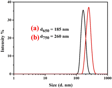 |
| | Fig. 6 Intensity vs. particle size of MWCNTs synthesized at temperatures of (a) 650 °C and (b) 750 °C. | |
3.6 Raman analysis
Fig. 7(a) and (b) show that the Raman spectrum of the MWCNTs synthesized at 650 °C and 750 °C, respectively. The Raman spectra of the synthesized MWCNT at different temperatures show two basic bands, and the first band is found at 1310 cm−1 and is known as the D band, and the second band is found at 1590 cm−1 and is known G band. The intensity of the D band decreases by increasing the growth temperature. The ID/IG ratio of the CNTs synthesized at 650 °C is 1.58 and that at 750 °C is 1.31, and it was found that the CNT synthesized at 750 °C had a high yield with less defective sites and an increase in the graphitic nature of the CNTs. The sp3 content present in the nanocrystalline carbon film was evaluated by the relationship given in eqn (5):48| | | sp3 content = 0.24 − 48.9 × (γG − 0.1580) | (5) |
where, γG is the position of the G band in the inverse micrometer scale. The values of sp3, sp2 and the ratio of sp3 and sp2 are summarized in Table 1. It was found that the sp2 content increased as the temperature of the synthesis increased and it was revealed that the surface sp2 phase in the amorphous carbon film may be the key factor in obtaining a low turn-on field and a high current density.
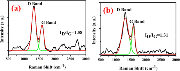 |
| | Fig. 7 (a) The Raman spectra of MWCNTs synthesized at 650 °C and (b) the Raman spectra of MWCNTs synthesized at 750 °C. | |
Table 1 Content of sp2 and sp3 in MWCNTs synthesized at different temperatures
| MWCNTs (synthesized at different temperatures) |
sp3 content (%) |
sp2 content (%) |
sp2/sp3 |
| MWCNT(650°C) |
17.63 |
82.37 |
4.6721 |
| MWCNT(750°C) |
11.75 |
88.23 |
7.4931 |
4. Field emission and photodetection analysis
4.1 Field emission analysis
Field emission is among the most flexible features of a MWCNT dependent thin-film. The field behavior of both pure MWCNT samples was thoroughly investigated and analyzed, focusing on the relationship between emission current density and the applied field, as outlined by the Fowler–Nordheim equation (eqn (6)):45,46| | 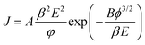 | (6) |
where A and B are the constants given by 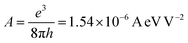 and
and 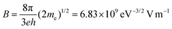 , where e, h and me are the elementary positive charge, Planck's constant and electron mass, respectively. Here J is the current density, ϕ is the potential barrier height or the work function of the emitter material, E is the applied field and β is the field enhancement factor that usually depends on the emitter configuration, the crystal structure, the vacuum gaps and the spatial distribution of the emitting centers. The two main parameters to be resolved in the MWCNTs films’ established that the field emission properties are the ‘threshold field’ and the ‘emission current’. The threshold field must be as low as possible, and the emission current should be high enough to allow the MWCNT-based thin film to be an effective field emitting material. The threshold field and the emission current of the MWCNT films depend on the bonding forms, which can be regulated either by the synthesis method or by the temperature of the growth of the elements. We have used a novel tubular structure of MWCNT to obtain effective field emission. We also reported the field emission characteristics of synthesized pure MWCNT at 650 °C and 750 °C. Fig. 8(a) shows the JE curves of the MWCNTs measured from their I–V (current–voltage) characteristics. It is evident from the figure that the threshold field decreased from 0.25 V μm−1 to 0.15 V μm−1, and the emission current increased from 0.1 μA to 0.3 μA, respectively, to increase the growth temperature from 650 °C to 750 °C. The field emission properties evaluated in this work are comparable with others reported in the literature as shown in Table 2. The high density and the larger length of grown MWCNTs provide a greater number of active field emission sites. The evaluation of the bandgap in MWCNTs revealed a lower threshold, indicative of the high electronegativity of these nanomaterials with low emission thresholds. Such results are comparable to those found in the literature,1,2,47–55 in which the nanotube at lower threshold voltages with their high aspect ratio were proven to be useful for field emission.
 |
| | Fig. 8 (a) The I–V curve of the MWCNT cathode prepared by MWCNT synthesized at 650 °C and 750 °C (b) Fowler–Nordheim (FN) plots of emission data for MWCNT prepared at 650 °C and 750 °C. | |
Table 2 Field emission parameters of different types of nanomaterials
| S. no. |
Nanomaterials |
Turn-on field (V μm−1) |
Field enhancement factor (β) |
Ref. |
| 1 |
Graphene aggregated films |
1.0 |
5110 |
51
|
| 2 |
Few layered graphene nanosheets |
1.7 |
7300 |
48
|
| 3 |
Vertically aligned few layered graphenes |
1.0 |
5000 |
52
|
| 4 |
CNT–Ni composite emitter |
1.1 |
2860 |
49
|
| 5 |
Ultrathin boron nitride (BN) nanosheets produced from BN fibers |
1.9 |
10 |
47
|
| 6 |
Si nanowire (NW) with NiSi2 tip array |
0.82 |
2440 |
50
|
| 7 |
Polypyrrole/tin oxide |
1.5 |
5665 |
51
|
| 8 |
Amorphous carbon |
4.9 |
1805 |
52
|
| 9 |
MoSSe–MWCNTs |
1.2 |
4468 |
53
|
| 10 |
Curved MWCNT synthesized using DLICVD |
0.1 |
9243 |
Present paper |
Fig. 8(a) shows the I–V curve of the MWCNT cathodes made with MWCNT samples prepared at 650 °C and 750 °C processed in a vacuum chamber for 10 min. Fig. 8(a) shows that as the voltage per unit length increases, the emission current also increases. After 0.06 V μm−1, the emission current decreased, because of the tunneling effect, to 0.17 V μm−1 and was constant to 0.2 V μm−1. Later the current of the emissions increased with the voltage rise. The Raman findings also support the field emission characteristics of these MWCNTs, which state that while defective graphite raises the MWCNT emission threshold, the graphitic nature during emission amplifies the electron.
This fact indicates that the nanotube's current emission level was heavily dependent upon field enhancement. For the unambiguous analysis of the change in the density of emission sites induced by changes in synthesis temperature, the variations in the field enhancement factor (β) were quantitatively calculated. The field enhancement factor (β) was calculated using eqn (7):
| |  | (7) |
where
B is constant,
d is the spacer thickness and
ϕ = 5 eV (graphite work function). Here the
β values were increased from 7708.50 to 9243.16 when the temperature of the synthesis increases from 650 °C to 750 °C. The reduction of the particle size in MWCNTs shows an improvement of the local field generation in the MWCNTs which increases the
β value. The results obtained were considered to be compatible with the morphological and structural changes observed (
Fig. 2(a) and (b)), but the FN curve in
Fig. 8(b) did not obey the FN model well during the initial field emission ranges, because the field enhancement factor values for each condition had many ranges depending on the varying lengths of the MWCNTs. It should be demonstrated that the
I–
V curve follows the Fowler–Nordheim equation after the applied field surpasses the turn-on barrier, which is a phenomenon impacting all MWCNTs.
The MWCNTs field emission property indicates that they have high current levels and low emission threshold voltages.56,57 This was very similar to the recorded properties of the CNTs synthesized in laser ablation, microwave CVD and plasma-enhanced CVD.57–59 Such MWCNTs also have improved emission levels when compared to bare metal and the silicon chip. When considering the application of MWCTs in the FED, the synthesis and growth of the MWCNTs on the catalyst at different temperatures is demanding for the manufacture of low-cost FEDs. A comparative analysis with their turn-on field and field enhancement factor were performed for a few carbon nanomaterials and the data is shown in Table 2.
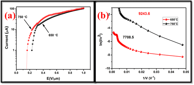
4.2 Mechanism of FED
Fig. 9 demonstrates a potential model interpretation of the field emission behavior process in MWCNTs. As is known the MWCNTs have a combination of sp2 and sp3 bonded carbon atoms. Due to a very high aspect ratio, in the presence of an externally applied field, the MWCNTs created a local electric field. Because of the network pathway between the sp2 bonded carbon atoms and the sp3 sites between them, the threshold field in the present model decreases together with the increase in emission current, which gives their optimum ratio.
 |
| | Fig. 9 The transport of electrons between the sp2 cluster embedded in the sp3 rich matrix. | |
In conjunction with the size of the work function, Fig. 10 shows that the magnetic field's intensity is what causes the emission from the metal surface. Thermionic emission may typically occur across the surface barrier (work function) as the electric field increases, followed by a lowered barrier (Schottky) emission over the field. The emission would therefore take place partially through the barrier and partially above it (at a high enough temperature). The electron states may emit radiation as a result of Fermi-level electron tunneling (also known as Fowler–Nordheim tunnelling) across the barrier when the temperature drops. The FN theory was used to describe the emission from gated emission arrays, CVD grown diamond film and carbon nanotube (CNTs). The basic FN theory is based on the premise that the metal has a free structure based on electrons. In terms of the Wentzel–Kramers–Brillouin approximation, the electron in the metal obeys Fermi Dirac statistics and the operation of the electron tunneling can be defined. The emission barrier can be represented by a triangular potential superimposed on a classical image potential.60
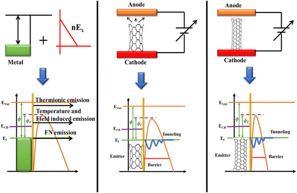 |
| | Fig. 10 The field emission mechanism in the presence of the electric field and FE enhancement with the increasing tube length. | |
4.3 Application as a photodetector
Under the ambient atmospheric conditions, atmospheric oxygen molecules are adsorbed on the surface of the MWCNTs. So, an electrical depletion layer is formed between the atmospheric oxygen molecules and the MWCNT surface. When light is incident upon the material, these atmospheric oxygen molecules are removed from the surface of the MWCNT.61–63 Thus, the depletion layer is removed between the MWCNT and the oxygen molecules under illumination, so, an increased level of photocurrent was observed. For evaluating the photoresponse of the MWCNT, different intensities of illumination were used and their corresponding parameters such as responsivity, detectivity, external quantum efficiency, linear dynamic range and on–off ratio64,65 were calculated and are presented in Table 3. In assessing the performance of a photodetector, parameters such as responsivity and detectivity stand out as crucial factors to analyze. The photoresponse of the photodetector device is shown in Fig. 11(a) and (b) at the different illumination times of 5 s and 10 s and it is suggested that the photocurrent rises as the illumination time rises at the applied potential of 1 V. The photoresponse of the device at different illumination intensities is also presented in Fig. 10(c). The responsivity of the photodetector device is defined as the generated photocurrent per incident photon for the unit illumination area (eqn (8)).66–68 Upon increasing the illumination intensity, the responsivity decreases so that for the illumination intensity of 25 mW cm−2, the responsivity was found to 1.0 A W−1, whereas this responsivity decreased to 0.5 A W−1 for the illumination intensity of 100 mW cm−2. The decrease in the responsivity upon increasing the illumination intensity is because of the fact that at whichever rate the illumination intensity increases, the photocurrent does not increase in proportion. It was noticed that the photoresponsivity of both MWCNT samples decreased with increasing illumination intensity. At high light intensities, the charge carriers become saturated and carrier recombination begins to occur, which is the cause of this phenomenon. The responsivity diminishes with increasing illumination intensity when the number of photoexcited carriers exceeds the number of available trapping sites or when the rate of carrier recombination exceeds the rate of carrier production. The next important parameter is the detectivity, which denotes the sensitivity of the photodetector device towards the low intensity of the light.69,70 From eqn (9), 100 mW cm−2 the detectivity was observed to 1.090 × 10¹⁰ jones, whereas for the intensity of 25 mW cm−2, the detectivity decreased to 2.1 × 10¹⁰ jones:| |  | (8) |
| |  | (9) |
Table 3 The photodetection parameters of the MWCNT-based device
| Intensity (mW cm−2) |
(Ip/Id) |
Responsivity (A W−1) |
LDR (dB) |
EQE (%) |
Detectivity (jones) |
NEP (W) |
| 25 |
4.6 |
1.03 |
13.40 |
349.55 |
2.17 × 10¹⁰ |
2.71 × 10⁻⁴ |
| 50 |
5.9 |
0.68 |
15.42 |
232.90 |
1.45 × 10¹⁰ |
4.07 × 10⁻⁴ |
| 75 |
7.0 |
0.56 |
16.97 |
191.78 |
1.19 × 10¹⁰ |
4.94 × 10⁻⁴ |
| 100 |
8.3 |
0.51 |
18.45 |
174.94 |
1.09 × 10¹⁰ |
5.42 × 10⁻⁴ |
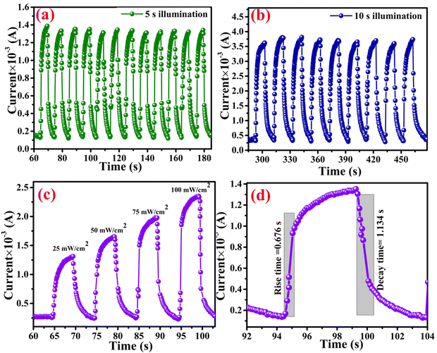 |
| | Fig. 11 Photoresponse of the MWCNT-based photodetector device (a) for 5 s illumination time, (b) for 10 s illumination time, (c) the photoresponse at different illumination intensities, and (d) the rise and decay time constants. | |
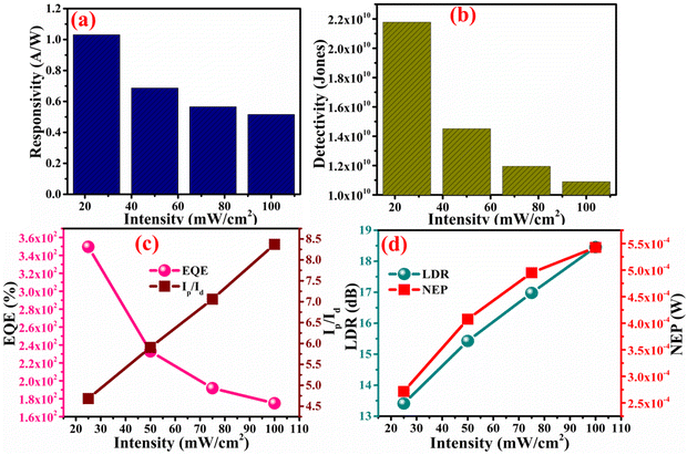
Another important parameter of the photodetector device is the external quantum efficiency (EQE), which defined as the generation of the photocurrent per incident photon (eqn (10)).68 From Fig. 12(c), it can be observed that, a metal–semiconductor–metal (MSM) device shows an EQE of 174.9% at the illumination intensity of 100 mW cm−2, which as it is higher than 100%, suggests there is photomultiplication behavior in the photodetector device. The phenomenon of photomultiplication allows the EQE of the MSM-based photoconductors to surpass 100%. On the semiconductor layer of the device, photomultiplication happens when a single absorbed photon produces numerous electron–hole pairs. In traditional photoconductive devices, the EQE is capped at 100% at most and each absorbed photon produces one electron–hole pair. However, in MSM-based photoconductors, the photogenerated carriers can acquire enough kinetic energy to ionize additional semiconductor atoms if the electric field is strong enough, producing several electron–hole pairs for each absorbed photon. The EQE of the device can be greatly raised above 100% by this photomultiplication effect. The noise equivalent power (NEP) of the photodetector device is defined as the required intensity to generate photocurrent at the level of dark current (eqn (11)). As the illumination intensity increases the NEP of the device also increases so that at the illumination intensity of 100 mW cm−2, the NEP was found to be 5.4 × 10⁻⁴ W, whereas for the intensity of 25 mW cm−2, this NEP was decreased to 2.7 × 10⁻⁴ W, as shown in Fig. 12(d).
| |  | (10) |
| |  | (11) |
| |  | (12) |
 |
| | Fig. 12 (a) The responsivity of the device with respect to the illumination intensity, (b) detectivity of the device with respect to the illumination intensity, (c) the EQE and on–off ratio of the device with respect to the illumination intensity, and (d) the LDR and NEP of the device with respect to the illumination intensity. | |
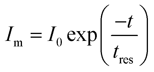
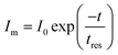
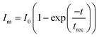
The linear dynamic range (LDR) of the photodetector device is defined as the linearity of the photodetector response towards the illumination intensity range (eqn (12)).71–73 The highest LDR of 18.4 dB was obtained for the device at the illumination intensity of 100 mW cm−2. Another important figure of merit of the photodetector device is the rise and decay time constants of the photodetector device.74,75 These rise and decay time constants were obtained by the exponential fitting of the rise and decay functions as given in eqn (13) and (14). The exponentially fitted rise and decay time constants were found to 0.6 s and 1.1 s, respectively, which signifies that there is fast exciton movement in the MWCNT material.
| |  | (13) |
| |  | (14) |
4.4 Theoretical investigation
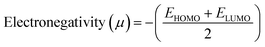
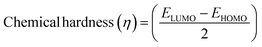
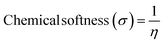
We have developed a theoretical model with different lengths of CNTs using Gaussview 05 and Gaussian 09 for FED and photodetectors, to clarify the observed effect. The calculation was performed in such molecular model using armchair (1,1) (2,2) (3,3) and (4,4) nanotube, and measurement method was B3LYP with basis set 6-31G. In the complete calculation, the spin is taken as single with the null charge of the C1 point group. In this computational method, we evaluated the electron affinity and ionization potential using the HOMO–LUMO band gap which was increased on increasing the tube length. Different electronic parameters were calculated by using eqn (15)–(20), which are also shown in Table 4.
Table 4 Theoretical analysis of variance in different parameters by increasing the length of carbon nanotubes
| Theoretical parameter (a.u.) |
CNT (1,1) |
CNT (2,2) |
CNT (3,3) |
CNT (4,4) |
| Electron affinity |
0.16361 |
0.16720 |
0.15270 |
0.15452 |
| Ionization potential |
0.19257 |
0.19249 |
0.20790 |
0.17534 |
| HOMO–LUMO gap |
0.02896 |
0.02529 |
0.0520 |
0.02082 |
| Electronegativity |
0.17809 |
0.17985 |
0.1803 |
0.1649 |
| Hardness |
0.01448 |
0.01264 |
0.0276 |
0.0104 |
| Softness |
69.061 |
79.08 |
36.23 |
96.06 |
| Nucleophilicity index |
−1.095 |
−1.27 |
−0.588 |
−1.306 |
Table 4 displays the energy changes observed and the different theoretical parameters that vary with the increasing the nanotube length. We calculated the higher occupied molecular orbit (HOMO) and lower unoccupied molecular orbit (LUMO) for the electronegativity, hardness, softness and nucleophilicity index using the formula as reported in a previously published paper.33,39 From the Table 4, we found that the electron affinity, ionization potential and the HOMO–LUMO gap decreased by increasing the length so we concluded that if the length of the nanotube increases more than 100 nm the value of electron affinity and ionization potential is negative and the bandgap decreased to ∼0 eV which was more useful for the FED. The electron affinity is related to the sp2 hybridized carbon, which is responsible for the bending of the step potential and the ionization potential is related to the sp3 hybridized carbon which is responsible for electron tunneling. From the above data, we concluded that for CNT having a higher length gives a higher emission current which was similar to our experimental data.
| | | HOMO − LUMO gap (ΔE) = ELUMO − EHOMO | (15) |
| | | Electron affinity (EA) = −ELUMO | (16) |
| | | Ionization potential (IP) = −EHOMO | (17) |
| |  | (18) |
| |  | (19) |
| |  | (20) |
5. Conclusion
Temperatures between 650 °C and 750 °C were used to grow the MWCNTs. The ability of CNTs to be used as field emitters was investigated by monitoring the evaporation temperature throughout the formation of the nanotubes, which produced an increased field enhancement factor (β) of 971. The surface morphology of the CNTs was shown to be changed by heat treatment, and the device structure may be employed as a parameter for the FE applications. In addition, it is inferred that the enhanced creation of the electron emission sites is the result of better FE characteristics. According to the photodetection measurements, MWCNT is both highly conductive and photoconductive. For example, for illumination of 25 mW cm−2, the response was found to be 1.031 A W−1, and the detectivity was found to be 1.090 × 10¹⁰ jones. At the highest intensity of 100 mW cm−2, the detectivity was found to 1.090 × 10¹⁰ jones. These enhanced parameters of the field-emission and photodetection will enable future advancement in the modern electronic and optoelectronic technologies.
Conflicts of interest
The authors declare that they have no conflicts of interest.
Acknowledgements
Dr Utkarsh Kumar is grateful to the UGC for providing the UGC National Fellowship for Scheduled Caste (F1-17.1/2017-18/RGNF-2017-18-SC-UTT-41083).
References
- N. Dwivedi, S. Kumar, J. D. Carey, R. K. Tripathi, H. K. Malik and M. K. Dalai, ACS Appl. Mater. Interfaces, 2013, 5, 2725–2732 CrossRef CAS PubMed.
- N. Dwivedi, S. Kumar, R. K. Tripathi, J. D. Carey, H. K. Malik and M. K. Dalai, ACS Appl. Mater. Interfaces, 2012, 4, 5309–5316 CrossRef CAS PubMed.
- N. Dwivedi, S. Kumar, R. K. Tripathi, H. K. Malik and O. S. Panwar, Appl. Phys. A: Mater. Sci. Process., 2011, 105, 417–425 CrossRef CAS.
- U. Kumar, S. Sikarwar, R. K. Sonker and B. C. Yadav, J. Inorg. Organomet. Polym. Mater., 2016, 26, 1231–1242 CrossRef CAS.
- R. K. Tripathi, O. S. Panwar, A. K. Srivastava, M. Kumar and S. Chockalingam, J. Nanosci., 2013, 2013, 1–11 CrossRef.
- S. Iijima, Nature, 1991, 354, 56–58 CrossRef CAS.
- U. Kumar and B. C. Yadav, J. Taiwan Inst. Chem. Eng., 2019, 96, 652–663 CrossRef CAS.
- U. Kumar and B. C. Yadav, Adv. Sci., Eng. Med., 2018, 10, 638–644 CrossRef CAS.
- R. Malik, V. K. Tomer, T. Dankwort, Y. K. Mishra and L. Kienle, J. Mater. Chem. A, 2018, 6, 10718–10730 RSC.
- F. Schütt, S. Signetti, H. Krüger, S. Röder, D. Smazna, S. Kaps, S. N. Gorb, Y. K. Mishra, N. M. Pugno and R. Adelung, Nat. Commun., 2017, 8, 1–10 CrossRef PubMed.
- E. L. Silva, Y. K. Mishra, A. J. S. Fernandes, R. F. Silva, J. Strobel, L. Kienle, R. Adelung, F. J. Oliveira and M. L. Zheludkevich, Adv. Mater. Interfaces, 2017, 4, 1700019 CrossRef.
- H. Sharma, V. Kaushik, S. Pathak, D. C. Agarwal, A. K. Shukla, D. K. Avasthi and V. D. Vankar, J. Mater. Sci.: Mater. Electron., 2023, 34, 1152 CrossRef CAS.
- E. Singh, R. Srivastava, U. Kumar and A. D. Katheria, Nanosci. Nanotechnol. Res., 2017, 4, 120–126 CAS.
- E. Hong, Z. Li, T. Yan and X. Fang, Nano Lett., 2022, 22, 8662–8669 CrossRef CAS PubMed.
- C.-S. Dai, P.-Y. Chien, J.-Y. Lin, S.-W. Chou, W.-K. Wu, P.-H. Li, K.-Y. Wu and T.-W. Lin, ACS Appl. Mater. Interfaces, 2013, 5, 12168–12174 CrossRef CAS PubMed.
- A. Singh, K. Senapati, M. Kumar, T. Som, A. K. Sinha and P. K. Sahoo, Appl. Surf. Sci., 2017, 411, 117–123 CrossRef CAS.
- Y. Y. Wang, S. Gupta, M. Liang and R. J. Nemanich, J. Appl. Phys., 2005, 97, 104309 CrossRef.
- P. K. Bankar, S. Ratha, M. A. More, D. J. Late and C. S. Rout, Appl. Surf. Sci., 2017, 418, 270–274 CrossRef CAS.
- H. Jadhav, S. Suryawanshi, M. More and S. Sinha, Appl. Surf. Sci., 2017, 419, 764–769 CrossRef CAS.
- J. E. Jung, Y. W. Jin, J. H. Choi, Y. J. Park, T. Y. Ko, D. S. Chung, J. W. Kim, J.
E. Jang, S. N. Cha and W. K. Yi, Phys. B, 2002, 323, 71–77 CrossRef CAS.
- R. Kumar, R. K. Singh, A. K. Singh, A. R. Vaz, C. S. Rout and S. A. Moshkalev, Appl. Surf. Sci., 2017, 416, 259–265 CrossRef CAS.
- S. Matsunaga, Y. Suwa and S. Katagiri, Surf. Sci., 2017, 666, 9–13 CrossRef CAS.
- A. Muhulet, F. Miculescu, S. I. Voicu, F. Schütt, V. K. Thakur and Y. K. Mishra, Mater. Today Energy, 2018, 9, 154–186 CrossRef.
- Y. Saito and S. Uemura, Carbon, 2000, 38, 169–182 CrossRef CAS.
- Y. Shiratori, K. Furuichi, Y. Tsuji, H. Sugime and S. Noda, Nanotechnology, 2009, 20, 475707 CrossRef PubMed.
- M. Sveningsson, R. E. Morjan, O. Nerushev and E. E. B. Campbell, Carbon, 2004, 42, 1165–1168 CrossRef CAS.
- X. Wu, Y. Wang and P. Yang, Phys. Lett. A, 2017, 381, 2004–2009 CrossRef CAS.
- R. Atchudan, T. N. J. I. Edison, S. Perumal, D. RanjithKumar and Y. R. Lee, Int. J. Hydrogen Energy, 2019, 44, 2349–2360 CrossRef CAS.
- R. Atchudan and A. Pandurangan, J. Mol. Catal. A: Chem., 2012, 355, 75–84 CrossRef CAS.
- R. Atchudan and A. Pandurangan, Microporous Mesoporous Mater., 2013, 167, 162–175 CrossRef CAS.
- R. Atchudan, A. Pandurangan and K. Subramanian, Appl. Surf. Sci., 2011, 258, 1045–1051 CrossRef CAS.
- T. Haldar, U. Kumar, B. C. Yadav and V. V. Kumar, J. Mater. Sci.: Mater. Electron., 2020, 31, 11791–11800 CrossRef CAS.
- P. Chaudhary, D. K. Maurya, A. Pandey, A. Verma, R. K. Tripathi, S. Kumar and B. C. Yadav, Sens. Actuators, B, 2022, 350, 130818 CrossRef CAS.
- A. Singh, P. Chauhan, A. Verma and B. C. Yadav, Phys. Chem. Chem. Phys., 2023, 25, 21383–21396 RSC.
- S. Saini, S. Ghosh and P. Srivastava, Appl. Surf. Sci., 2023, 635, 157653 CrossRef CAS.
- J. E. Herrera and D. E. Resasco, J. Catal., 2004, 221, 354–364 CrossRef CAS.
- S. Maruyama, R. Kojima, Y. Miyauchi, S. Chiashi and M. Kohno, Chem. Phys. Lett., 2002, 360, 229–234 CrossRef CAS.
- E. Singh, U. Kumar, R. Srivastava and B. C. Yadav, Adv. Sci., Eng. Med., 2018, 10, 785–787 CrossRef CAS.
- U. Kumar and B. C. Yadav, Sens. Actuators, B, 2019, 288, 399–407 CrossRef CAS.
- A. Chatterjee, M. Sharon, R. Banerjee and M. Neumann-Spallart, Electrochim. Acta, 2003, 48, 3439–3446 CrossRef CAS.
- M. Shariat, S. Hosseini, B. Shokri and E. C. Neyts, Carbon, 2013, 65, 269–276 CrossRef CAS.
- A. Verma, U. Kumar, P. Chaudhary and B. C. Yadav, Solid State Commun., 2022, 348, 114723 CrossRef.
- H. Ago, T. Kugler, F. Cacialli, W. R. Salaneck, M. S. P. Shaffer, A. H. Windle and R. H. Friend, J. Phys. Chem. B, 1999, 103, 8116–8121 CrossRef CAS.
- L. Ci, B. Wei, C. Xu, J. Liang, D. Wu, S. Xie, W. Zhou, Y. Li, Z. Liu and D. Tang, J. Cryst. Grow., 2001, 233, 823–828 CrossRef CAS.
-
F. Léonard, Physics of carbon nanotube devices, William Andrew, 2008 Search PubMed.
- S. K. Srivastava, V. Vankar, D. S. Rao and V. Kumar, Thin Solid Films, 2006, 515, 1851–1856 CrossRef CAS.
- Z.-G. Chen and J. Zou, J. Mater. Chem., 2011, 21, 1191–1195 RSC.
- J. Dong, B. Zeng, Y. Lan, S. Tian, Y. Shan, X. Liu, Z. Yang, H. Wang and Z. F. Ren, J. Nanosci. Nanotechnol., 2010, 10, 5051–5055 CrossRef CAS PubMed.
- B.-R. Huang, T.-C. Lin, Y.-K. Yang and S.-D. Tzeng, Diamond Relat. Mater., 2010, 19, 158–161 CrossRef CAS.
- C.-Y. Liu, W.-S. Li, L.-W. Chu, M.-Y. Lu, C.-J. Tsai and L.-J. Chen, Nanotechnology, 2010, 22, 055603 CrossRef PubMed.
- I. Rawal, L. Kumar, R. K. Tripathi and O. S. Panwar, ACS Omega, 2017, 2(11), 7515–7524 CrossRef CAS PubMed.
- R. K. Tripathi, O. S. Panwar, A. K. Srivastava, I. Rawal and S. Chockalingam, Talanta, 2014, 125, 276–283 CrossRef CAS PubMed.
- C. D. Mistari, P. Mane, P. Koinkar, B. Chakraborty and M. A. More, J. Alloys Compd., 2023, 965, 171356 CrossRef CAS.
- Z. Lu, W. Wang, X. Ma, N. Yao, L. Zhang and B. Zhang, J. Nanomater., 2010, 2010, 148596 Search PubMed.
- A. Malesevic, R. Kemps, A. Vanhulsel, M. P. Chowdhury, A. Volodin and C. Van Haesendonck, J. Appl. Phys., 2008, 104, 084301 CrossRef.
- L. Nilsson, O. Groening, C. Emmenegger, O. Kuettel, E. Schaller, L. Schlapbach, H. Kind, J. M. Bonard and K. Kern, Appl. Phys. Lett., 2000, 76, 2071–2073 CrossRef CAS.
- R. K. Sonker, M. Singh, U. Kumar and B. C. Yadav, J. Inorg. Organomet. Polym. Mater., 2016, 26, 1434–1440 CrossRef CAS.
- H. Choi, Y. J. Shin, S. I. Cha, I. H. Kang and W. Bahng, Solid State Commun., 2013, 171, 50–54 CrossRef CAS.
- J. G. Wen, Z. P. Huang, D. Z. Wang, J. H. Chen, S. X. Yang, Z. Ren, J. H. Wang, L. E. Calvet, J. Chen and J. F. Klemic, J. Mater. Res., 2001, 16, 3246–3253 CrossRef CAS.
- J. D. Carey, Philos. Trans. R. Soc., A, 2003, 361, 2891–2907 CrossRef CAS PubMed.
- A. Verma, P. Chaudhary, A. Singh, R. K. Tripathi and B. C. Yadav, ACS Appl. Nano Mater., 2022, 5, 4860–4874 CrossRef CAS.
- J. Z. Wu and M. Gong, Adv. Photonics Res., 2021, 2, 2100015 CrossRef CAS.
- X. Deng, Z. Li, F. Cao, E. Hong and X. Fang, Adv. Funct. Mater., 2023, 33, 2213334 CrossRef CAS.
- A. Verma, P. Chaudhary, R. K. Tripathi, A. Singh and B. C. Yadav, J. Inorg. Organomet. Polym. Mater., 2022, 1–20 Search PubMed.
- R. K. Tripathi, O. S. Panwar, A. K. Kesarwani, I. Rawal, B. P. Singh, M. K. Dalai and S. Chockalingam, RSC Adv., 2014, 4, 54388–54397 RSC.
- C. Gautam, A. Verma, P. Chaudhary and B. C. Yadav, Opt. Mater., 2022, 123, 111860 CrossRef CAS.
- A. Verma, P. Chaudhary, R. K. Tripathi and B. C. Yadav, Mater. Adv., 2022, 3994–4005 RSC.
- X. Zhang, Z. Li, E. Hong, M. Deng, L. Su and X. Fang, Adv. Funct. Mater., 2023, 2312293 CrossRef.
- R. K. Tripathi, O. S. Panwar, I. Rawal, C. K. Dixit, A. Verma, P. Chaudhary, A. K. Srivastava and B. C. Yadav, J. Mater. Sci.: Mater. Electron., 2021, 32, 2535–2546 CrossRef CAS.
- R. K. Tripathi, O. S. Panwar, I. Rawal, B. P. Singh and B. C. Yadav, J. Taiwan Inst. Chem. Eng., 2018, 86, 185–191 CrossRef CAS.
- A. Verma, P. Chaudhary, R. K. Tripathi and B. C. Yadav, Sustainable Energy Fuels, 2021, 5, 1394–1405 RSC.
- P. Aggarwal, S. Kaushik, P. Bisht, M. Sharma, A. Singh, B. R. Mehta and R. Singh, Cryst. Growth Des., 2022, 22, 3206–3217 CrossRef CAS.
- R. Wadhwa, A. Ghosh, D. Kumar, P. Kumar and M. Kumar, Nanotechnology, 2022, 33, 255702 CrossRef CAS PubMed.
- M. Patel, J. Song, D.-W. Kim and J. Kim, Appl. Mater. Today, 2022, 26, 101344 CrossRef.
- A. Verma, P. Chaudhary, R. K. Tripathi and B. C. Yadav, Sens. Actuators, A, 2021, 321, 112600 CrossRef CAS.
|
| This journal is © The Royal Society of Chemistry 2024 |
Click here to see how this site uses Cookies. View our privacy policy here. 
 Open Access Article
 This Open Access Article is licensed under a
  ab,
Arpit
Verma
ab,
Arpit
Verma


 and
and  , where e, h and me are the elementary positive charge, Planck's constant and electron mass, respectively. Here J is the current density, ϕ is the potential barrier height or the work function of the emitter material, E is the applied field and β is the field enhancement factor that usually depends on the emitter configuration, the crystal structure, the vacuum gaps and the spatial distribution of the emitting centers. The two main parameters to be resolved in the MWCNTs films’ established that the field emission properties are the ‘threshold field’ and the ‘emission current’. The threshold field must be as low as possible, and the emission current should be high enough to allow the MWCNT-based thin film to be an effective field emitting material. The threshold field and the emission current of the MWCNT films depend on the bonding forms, which can be regulated either by the synthesis method or by the temperature of the growth of the elements. We have used a novel tubular structure of MWCNT to obtain effective field emission. We also reported the field emission characteristics of synthesized pure MWCNT at 650 °C and 750 °C. Fig. 8(a) shows the JE curves of the MWCNTs measured from their I–V (current–voltage) characteristics. It is evident from the figure that the threshold field decreased from 0.25 V μm−1 to 0.15 V μm−1, and the emission current increased from 0.1 μA to 0.3 μA, respectively, to increase the growth temperature from 650 °C to 750 °C. The field emission properties evaluated in this work are comparable with others reported in the literature as shown in Table 2. The high density and the larger length of grown MWCNTs provide a greater number of active field emission sites. The evaluation of the bandgap in MWCNTs revealed a lower threshold, indicative of the high electronegativity of these nanomaterials with low emission thresholds. Such results are comparable to those found in the literature,1,2,47–55 in which the nanotube at lower threshold voltages with their high aspect ratio were proven to be useful for field emission.