DOI:
10.1039/D4YA00034J
(Paper)
Energy Adv., 2024,
3, 1375-1388
Thermally deposited copper(I) thiocyanate thin film: an efficient and sustainable approach for the hole transport layer in perovskite solar cells†
Received
19th January 2024
, Accepted 14th May 2024
First published on 16th May 2024
Abstract
Solution-processable deposition of copper(I) thiocyanate (CuSCN) thin films have been widely used to form the hole transport layer (HTL) in optoelectronic applications, namely perovskite and organic solar cells. Herein, we report the thermally deposited CuSCN thin film as an efficient, eco-friendly and solvent-free approach for HTL deposition in inverted perovskite solar cells as an alternative to conventional solution-processed methods. The structural, electrochemical, optical, and morphological properties of thermally deposited CuSCN films were characterized. The long-term electrochemical and optical stability of thermally deposited CuSCN films were examined. The effect of thicknesses (20, 30, 40, 60, and 100 nm) and annealing temperatures (RT, 50, 100, 150, and 200 °C) of CuSCN films on the photovoltaic performance were investigated. The optimized device configuration ITO/CuSCN/MAPbI3/PC61BM/BCP/Ag with a 30 nm thick CuSCN film annealed at 100 °C for 10 min exhibited the maximum power conversion efficiency (PCE) of 15.71% with Voc = 1.01 V, Jsc = 20.2 mA cm−2, and FF = 0.77. For reference, perovskite solar cells without a HTL were fabricated simultaneously. Importantly, the thermally deposited CuSCN-based devices showed excellent reproducibility and stability up to 240 h with ∼89% retention of the initial PCE. This study demonstrates a new methodology for obtaining better CuSCN films using a thermal deposition technique for efficient, sustainable and scalable electronic device applications.
Introduction
Perovskite solar cells are the most promising candidates for thin-film photovoltaic technology. They show significant enhancement in power conversion efficiency (PCE ≥ 26.1%), which is comparable with that of traditional silicon-based solar cells. Impressive progress has been made due to intensive research on the optimization of perovskite composition, device architecture and interface engineering.1–4 Simultaneously, the hole transport layer (HTL) has been identified as the major component of perovskite solar cells5–7 because it has an important contribution to the photovoltaic performance and the stability of devices.8,9 The HTL enables an effective charge extraction and the collection of photogenerated holes from the perovskite absorber layer, which is vital for attaining high device performance. Additionally, the HTL plays a key role in protecting the perovskite film from environmental degradation, minimizes charge recombination and acts as the blocking layer for highly efficient and stable perovskite solar cells.10,11
In general, hole transport materials (HTMs) can be categorized into organic and inorganic materials. Compared with organic HTMs [such as 2,2′,7,7′-tetrakis[N,N-di(4-methoxyphenyl)amine]-9,9′-spirobifluorene (spiro-OMeTAD),12 (3,4-ethylenedioxythiophene):poly(styrenesulfonate) (PEDOT:PSS),13,14 poly[bis(4-phenyl)(2,4,6-trimethylphenyl)amine] (PTAA),15 triphenylamine (TPA), spiro-OMeTAD derivatives and others],16–19 inorganic HTMs [such as copper oxides (CuOX), nickel oxides (NiOX),20 copper iodide (CuI),21,22 copper thiocyanate (CuSCN),23–26 and copper selenocyanate (CuSeCN)27–29] exhibit excellent chemical stability, high hole mobility, and high optical transparency.30,31 Moreover, the facile and low-cost preparation of inorganic HTMs has emerged as a cost-effective substitute for organic HTMs which have low transparency, high cost and usually a difficult synthetic route.
Among various inorganic HTMs, CuSCN, an air-stable material, has been widely used as a HTL in perovskite solar cells due to its wide bandgap (3.7–3.9 eV), high optical transparency, high hole mobility (0.01–0.1 cm2 V−1 s−1), excellent hole transporting property, low-temperature processability, and variety of morphologies obtained by different fabrication techniques.32–35 Perhaps the most attractive aspect of CuSCN material is that it is inexpensive, highly abundant, intrinsically stable, commercially available, and easily handled, making it a suitable HTL for perovskite solar cells. For CuSCN film as a HTL, the different deposition methods, such as doctor blading,36 electrodeposition,37,38 spin coating,39 and spray coating40 have been widely reported in the literature. In 2014, Qin et al. were the first to report the doctor-bladed CuSCN in n–i–p perovskite solar cells and achieved a PCE of 12.4%.37 CuSCN films of 600 nm thickness were prepared using dipropyl sulfide solvent. However, it was reported that it led to the partial dissolution of the perovskite layer by CuSCN. To reduce this dissolution effect, Sepalage et al. reported the use of chlorobenzene (acts as a protective layer) on top of the perovskite absorber layer before doctor blading the CuSCN solution, and attained the maximum PCE of 9.6%.41 To further reduce damage to the perovskite layer, Lee and coworkers developed a simple spray-coating method that allowed minimum contact between the dipropyl sulfide solvent and the perovskite layer, and obtained a higher PCE of 17.1%.41 Murugadoss and coworkers presented doctor-bladed CuSCN with proposed mixtures of depositing solvents for CuSCN and achieved PCE up to 10.0% with negligible damage to the perovskite film.42 Meanwhile, Madhavan and coworkers employed both doctor-bladed and spin-coated CuSCN in n–i–p perovskite solar cells and displayed a PCE of 16.6% (doctor-bladed CuSCN) and 15.43% (spin-coated CuSCN).43 A common obstacle associated with the solution-processed method is finding an “ideal” solvent for the deposition of CuSCN as HTL due to its low solubility.44 Also, in comparison with doctor blading, spin coating is not suitable for large-scale fabrication of solar cells due to origin of non-uniformity in the film and as well as huge amount of raw materials and solvents is wasted, thereby increasing the overall cost.45,46
The main problem that existed with the above-discussed solution-processed CuSCN as the HTL is the damaging effect of limited n-alkyl sulfide solvents to the perovskite layer as well as incorporation of minor impurities.47,48 Wijeyasinghe and co-workers reported aqueous ammonia-processed CuSCN-based perovskite solar cells as a substitute for n-alkyl sulfide solvents and demonstrated a PCE of 17.5%, but with a reduced device lifetime.49 Besides, Arora and co-workers developed a dynamic spin-coating technique for CuSCN deposition with aluminium oxide (Al2O3) or reduced graphene oxide (rGO) as an interfacial layer between CuSCN and gold (Au) to fabricate high-performance perovskite devices with 20.4% PCE and good thermal stability.50 The interfacial layer of polymethyl methacrylate (PMMA) was introduced between CH3NH3PbI3 and CuSCN to achieve an efficiency of 19.2% with thermal stability for 96 h.51 Lately, the additive engineering has been used to increase the conductivity of CuSCN which enhance hole extraction and transportation processes in both regular and inverted architectures of perovskite solar cells.52–54
Despite the tremendous progress of CuSCN-based perovskite solar cells, the relatively complex issues of depositing solvents of CuSCN and the complicated interface engineering approach may restrict their possible practical applications in the future. A solution-processed additive method is hindered by the presence of other compounds of Cu(II)-oxidized species due to inevitable exposure to the atmosphere. Also, wettability issues in solution processing often lead to pinhole formation and non-uniform coating. Surprisingly, despite a surge in research efforts, the thermally deposited CuSCN film as a HTL in perovskite solar cells has not been reported so far. In this connection, we employed thermally deposited CuSCN in perovskite solar cells as an alternative and facile technique to conventional solution-processed methods. Thermal deposition is a simple, affordable, and straightforward technique which could also be compatible for large-scale device fabrications. It is a well-known technique used for depositing metals such as Ag, Au, and Cu which works as a back electrode in perovskite solar cells. This method possesses numerous advantages, such as easily-controlled film thickness, uniform film formation, impurity-free composition and low temperature processability, making it compatible for both flexible and rigid substrates.55 The ability to obtain promising results from the thermal deposition of CuSCN opens the door for the integration of inorganic materials for large-scale fabrication of solar cells.
In the present work, the thermal deposition of CuSCN, a solvent-free and environmentally friendly (“green”) approach is reported for the fabrication of CuSCN thin film as a HTL on the indium tin oxide (ITO) surface. The deposition rate and deposition time were optimized to obtain different thicknesses of CuSCN films. The structural, electrochemical, optical and surface morphology of thermally deposited CuSCN films were characterized. The long-term electrochemical and optical stability of CuSCN films were measured. The thermally deposited CuSCN films as HTL were used to fabricate inverted planar perovskite solar cells with device configuration ITO/CuSCN/MAPbI3/PC61BM/BCP/Ag. The thickness and annealing temperature of the CuSCN film were optimized to obtain the maximum device performance. For reference, perovskite solar cells without a HTL were fabricated under similar conditions. Finally, the stability of the optimized devices without encapsulation was examined in the N2 environment as well as in ambient conditions. This work illustrates a new methodology for obtaining better CuSCN films by thermal deposition technique for sustainable and scalable electronic device applications.
Experimental section
Materials
Copper(I) thiocyanate (CuSCN, 99.0%), methylammonium iodide (MAI, 99.5%), lead iodide (PbI2, 99.0%), phenyl-C61-butyric acid methyl ester (PC61BM, 99.0%), bathocuproine (BCP), anhydrous N,N-dimethylformamide (DMF, 99.8%), anhydrous chlorobenzene (CB, 99.5%), anhydrous dimethyl sulfoxide (DMSO, 99.9%), and tetrabutylammonium perchlorate (TBAClO4, for electrochemical analysis ≥ 99.0%) were purchased from Sigma-Aldrich. Indium tin oxide (ITO)-glass was bought from Shilpa Enterprises, Nagpur, India, and the standard substrate size was 25.0 × 25.0 mm. All the materials and solvents stated above were used as received unless specified otherwise.
Device fabrication
Patterned ITO-coated glass substrates were cleaned consecutively in detergent, deionized water, acetone, and isopropanol for 30 min each in an ultrasonic bath. Then, the ITO/glass substrates were treated under air plasma etches for 10 min before use. CuSCN thin film as HTL with different thicknesses were deposited by thermal deposition of CuSCN in a high-vacuum chamber (2 × 10⁻⁶ mbar). The deposition rate was ∼0.5 Å s−1. After the deposition, the films were annealed at 100 °C on a hotplate for 10 min in ambient conditions. Once cooled to room temperature, samples were transferred to a N2-filled glove box. A perovskite precursor solution was prepared by mixing CH3NH3I and PbI2 in a mixture of DMF and DMSO (volume ratio of 9![[thin space (1/6-em)]](https://www.rsc.org/images/entities/char_2009.gif) :1) to obtain a concentration of 1.5 M. The perovskite solution was stirred overnight at 70 °C and passed through a 0.2 μm polytetrafluoroethylene (PTFE) filter prior to spin coating. The filtered perovskite precursor was spin-casted on the top of CuSCN film at 4000 rpm for 35 s. After 15 s of spinning, CB was quickly added to induce fast crystallization. The colour of the resulting substrate was dark-brown and, after annealing at 100 °C for 10 min, it gradually became black. PC61BM (20.0 mg mL−1 in chlorobenzene) as an electron-extracting layer was deposited by spin casting at 2000 rpm for 45 s, and samples were again annealed at 100 °C for 10 min. A solution of BCP in isopropanol (0.5 mg mL−1) was deposited on PC61BM films by spin casting at 6000 rpm for 30 s. Finally, 100 nm of silver (as a back contact) was deposited by thermal evaporation under a high vacuum pressure of 2 × 10⁻⁶ mbar through a shadow mask to make four devices per slide, each with an active cell area of 6.0 mm2.
:1) to obtain a concentration of 1.5 M. The perovskite solution was stirred overnight at 70 °C and passed through a 0.2 μm polytetrafluoroethylene (PTFE) filter prior to spin coating. The filtered perovskite precursor was spin-casted on the top of CuSCN film at 4000 rpm for 35 s. After 15 s of spinning, CB was quickly added to induce fast crystallization. The colour of the resulting substrate was dark-brown and, after annealing at 100 °C for 10 min, it gradually became black. PC61BM (20.0 mg mL−1 in chlorobenzene) as an electron-extracting layer was deposited by spin casting at 2000 rpm for 45 s, and samples were again annealed at 100 °C for 10 min. A solution of BCP in isopropanol (0.5 mg mL−1) was deposited on PC61BM films by spin casting at 6000 rpm for 30 s. Finally, 100 nm of silver (as a back contact) was deposited by thermal evaporation under a high vacuum pressure of 2 × 10⁻⁶ mbar through a shadow mask to make four devices per slide, each with an active cell area of 6.0 mm2.
Characterization
The structural properties of CuSCN films were characterized via X-ray diffraction (XRD) patterns over the 2θ range of 10° to 70° using a MiniFlex-II diffractometer (Cu Kα1 irradiation, λ = 1.5418 Å; Rigaku). Raman spectra were recorded on a T64000 triple Raman spectrometer with a 514 nm laser. Fourier transform infrared (FTIR) spectroscopy was performed on a spectrophotometer (Spectrum Two; PerkinElmer) in the wavenumber range 4000 to 400 cm−1 (wavelength 2.5 to 25 μm) using KBr pellets. CuSCN was collected from the film by scratching, and the sample was prepared with KBr. Electrochemical characterization was performed on a PGSTAT204 setup (Metrohm Autolab) equipped with a three-electrode system in a single compartment cell. Ag/AgCl wire (reference electrode), Au wire (counter electrode) and glassy carbon (GC; diameter = 2.0 mm; working electrode) were used. Prior to thermal deposition of CuSCN, the working electrode was polished with 0.05 μm alumina slurry for 60 s, and then rinsed with distilled water and dried in air. Cyclic voltammetry (CV) measurement of thermally deposited CuSCN film on the GC electrode was carried out in DMF solution containing 0.1 M tetrabutylammonium perchlorate (TBAClO4) as the supporting electrolyte. Ultraviolet-visible absorption and transmittance spectra were recorded on a spectrophotometer (UV-1800; Shimadzu) in the wavelength range 200 to 1100 nm. The surface morphology of thermally deposited CuSCN films on ITO-coated glass was investigated by atomic force microscopy (AFM) as well as field emission scanning electron microscopy (FESEM) using Tescan Magna gmh setup by applying a 15.0 keV accelerating voltage. The thickness of films was measured using a Stylus profilometer (500ES; NanoMap). Photocurrent–voltage (J–V) characteristic curves of the perovskite solar cells were measured using a digital source system (4200; Keithley Laboratories) with Lab Tracer software in ambient conditions. With standard illumination (AM 1.5 G), a solar simulator of class AAA (Photo Emission Technologies) was equipped. Before use, a silicon reference cell was utilized to calibrate the light source at 100 mW cm−2.
Results and discussion
Structural characterizations
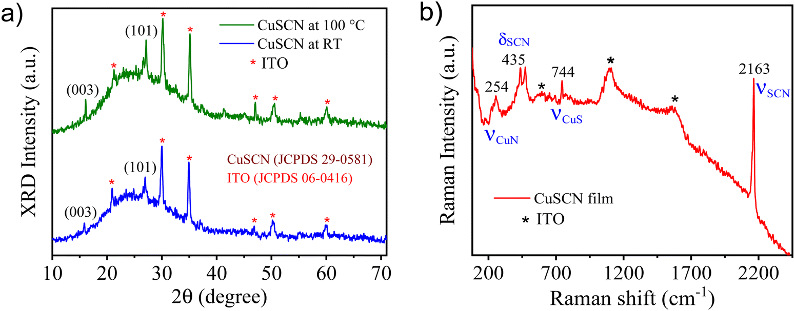
The phase and crystallinity of the thermally deposited CuSCN thin films were analyzed using X-ray diffraction (XRD) patterns, as shown in Fig. 1(a). Previous reports have stated that CuSCN thin films can exist in α-phase (orthorhombic) or β-phase (rhombohedral or hexagonal), and the latter is more common in the case of CuSCN thin films.56,57 The observed diffraction peaks for CuSCN thin films at 16.1° and 27.2° corresponded to the (003) and (101) planes of the β-phase, which were matched with the standard JCPDS card (29-0581),58,59 suggesting the crystallization of a CuSCN thin film in β-phase with a rhombohedral crystal structure. Herein, the intensity of the peaks increased with annealing the CuSCN film at 100 °C for 10 min (Fig. 1(a)), indicating higher crystallinity of the annealed CuSCN film. Other peaks marked with an asterisk (*) could be ascribed to ITO-coated glass (JCPDS number = 06-0416). Besides these observations, no other diffraction peaks were found, which confirmed the β-phase purity and crystallinity of the thermally deposited CuSCN film. Fig. S1 (ESI†) illustrates the XRD spectrum of a perovskite CH3NH3PbI3 film on ITO-coated glass which shows sharp peaks of high crystallinity. The diffraction peaks at 14.02°, 19.94°, 23.34°, 24.38°, 28.34°, 31.81°, 34.79°, 40.47°, 43.03° and 50.15° could be attributed to the (110), (200), (211), (202), (220), (310), (312), (224), (314) and (404) planes of tetragonal phase, respectively, and are in good agreement with earlier reports.60,61 The XRD pattern of the CH3NH3PbI3 film indicated that the perovskite film preferentially grew in the tetragonal crystal structure. Also, there are no PbI2 impurities present, which confirmed the formation of a pure phase of perovskite films (Fig. S1, ESI†).
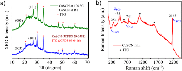 |
| | Fig. 1 (a) X-ray diffraction spectra and (b) Raman spectrum of a thermally deposited CuSCN film on an ITO-coated glass substrate. The characteristic peaks of β-CuSCN are indicated. The asterisk (*) denotes ITO peaks. | |
Raman spectroscopy was performed to further investigate the structure of the thermally deposited CuSCN film. Fig. 1(b) demonstrates the Raman spectrum of an annealed CuSCN film at 100 °C. The main characteristic peak was recorded at 2163 cm−1, which corresponded to the C![[triple bond, length as m-dash]](https://www.rsc.org/images/entities/char_e002.gif) N stretching (νCN) of thiocyanate (–S–CN) in β-CuSCN, indicating that the thermally deposited CuSCN film contained only the β-CuSCN polymorph. At lower Raman shifts, the peaks of CuSCN were attributed to Cu–N stretching (νCuN ∼254 cm−1), SCN bending (δSCN ∼435 cm−1, suggesting predominant thiocyanate S-binding) and Cu–S stretching (νCuS ∼744 cm−1).62,63 Other peaks marked with an asterisk were assigned to the ITO-coated glass substrate. As in-depth interaction between laser light with the ITO-coated glass substrate was inevitable because of the high optical transparency of the CuSCN thin film. Apart from this, no additional secondary phase or impurities were observed, which further confirmed the β-phase of the CuSCN thin film.
N stretching (νCN) of thiocyanate (–S–CN) in β-CuSCN, indicating that the thermally deposited CuSCN film contained only the β-CuSCN polymorph. At lower Raman shifts, the peaks of CuSCN were attributed to Cu–N stretching (νCuN ∼254 cm−1), SCN bending (δSCN ∼435 cm−1, suggesting predominant thiocyanate S-binding) and Cu–S stretching (νCuS ∼744 cm−1).62,63 Other peaks marked with an asterisk were assigned to the ITO-coated glass substrate. As in-depth interaction between laser light with the ITO-coated glass substrate was inevitable because of the high optical transparency of the CuSCN thin film. Apart from this, no additional secondary phase or impurities were observed, which further confirmed the β-phase of the CuSCN thin film.
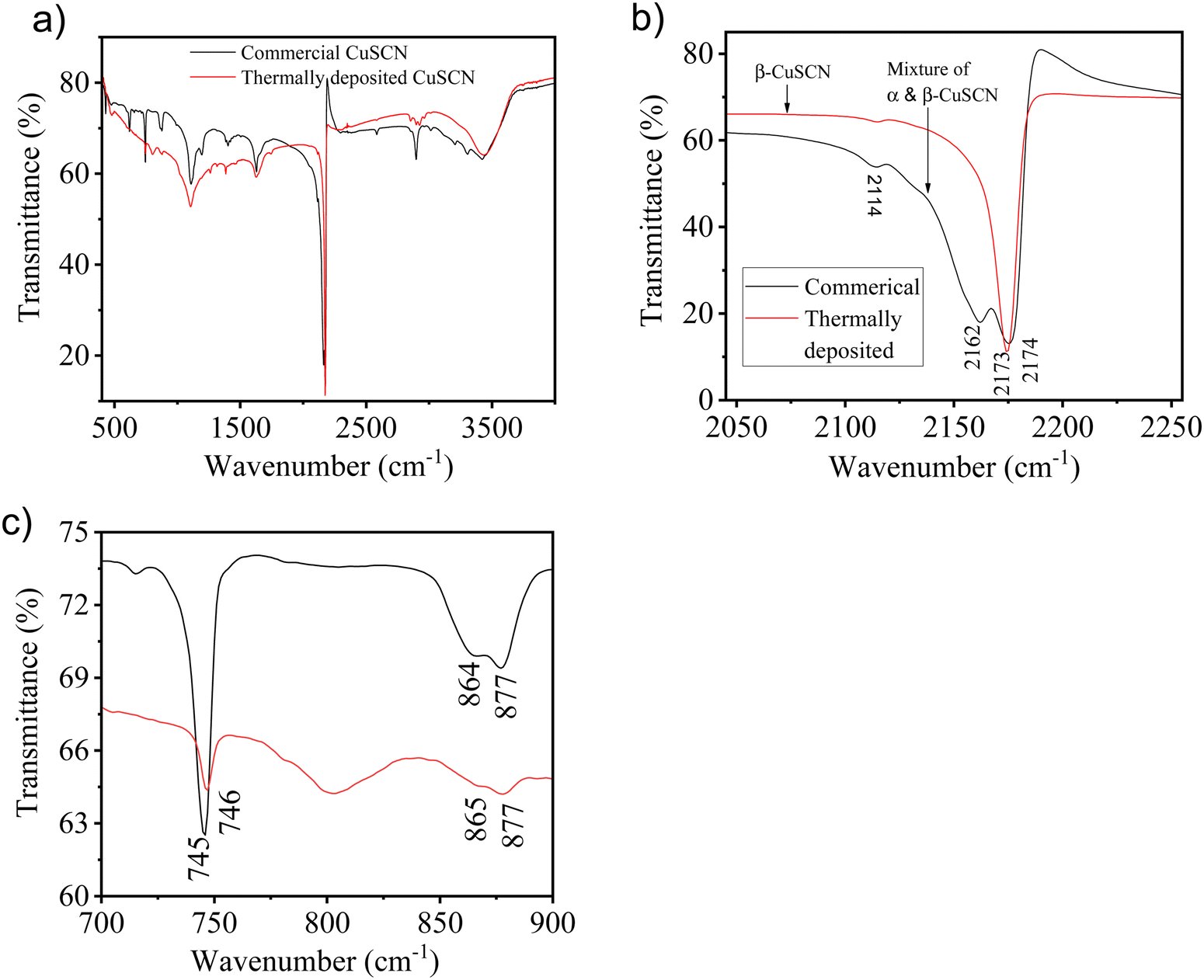
Further, FTIR spectroscopy of the thermally deposited CuSCN film was performed. Fig. 2(a) shows the full spectra of the thermally deposited CuSCN as well as commercial CuSCN (for comparison purposes). According to the literature, commercially available CuSCN powder consists of a mixture of α- and β-CuSCN.64 The FTIR spectrum of commercial CuSCN displayed peaks at 2162 and 2174 cm−1 associated with the CN vibrational bands of α- and β-phases, respectively (Fig. 2(b)). The FTIR spectrum of thermally deposited CuSCN showed a single peak at 2173 cm−1, which confirmed the formation of only β-CuSCN (Fig. 2(b)). In addition, commercial CuSCN displayed peaks at 864 cm−1 and 877 cm−1, which were assigned to ν(SCN) stretching, and the peak at 745 cm−1 was attributed to CS vibrations (Fig. 2(c)). The above-mentioned peak values were also obtained in the case of thermally deposited CuSCN (Fig. 2(c)). All observations and characteristic peak values were in excellent agreement with an earlier report.57 These results confirmed that the thermal deposition of CuSCN under high vacuum resulted in the formation of β-phase CuSCN. Also, the FTIR spectra of thermally deposited CuSCN nicely complemented the Raman spectra, which further confirmed the formation of the β-phase of CuSCN during thermal deposition.
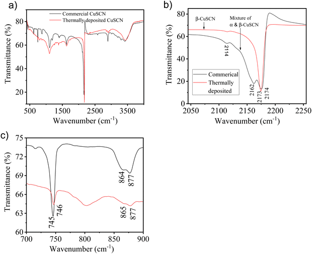 |
| | Fig. 2 (a) FTIR spectra of the commercial and thermally deposited CuSCN. Expanded FTIR spectra of both CuSCN in the wavenumber range of (b) 2050–2250 cm−1 and (c) 700–900 cm−1. | |
Electrochemical properties
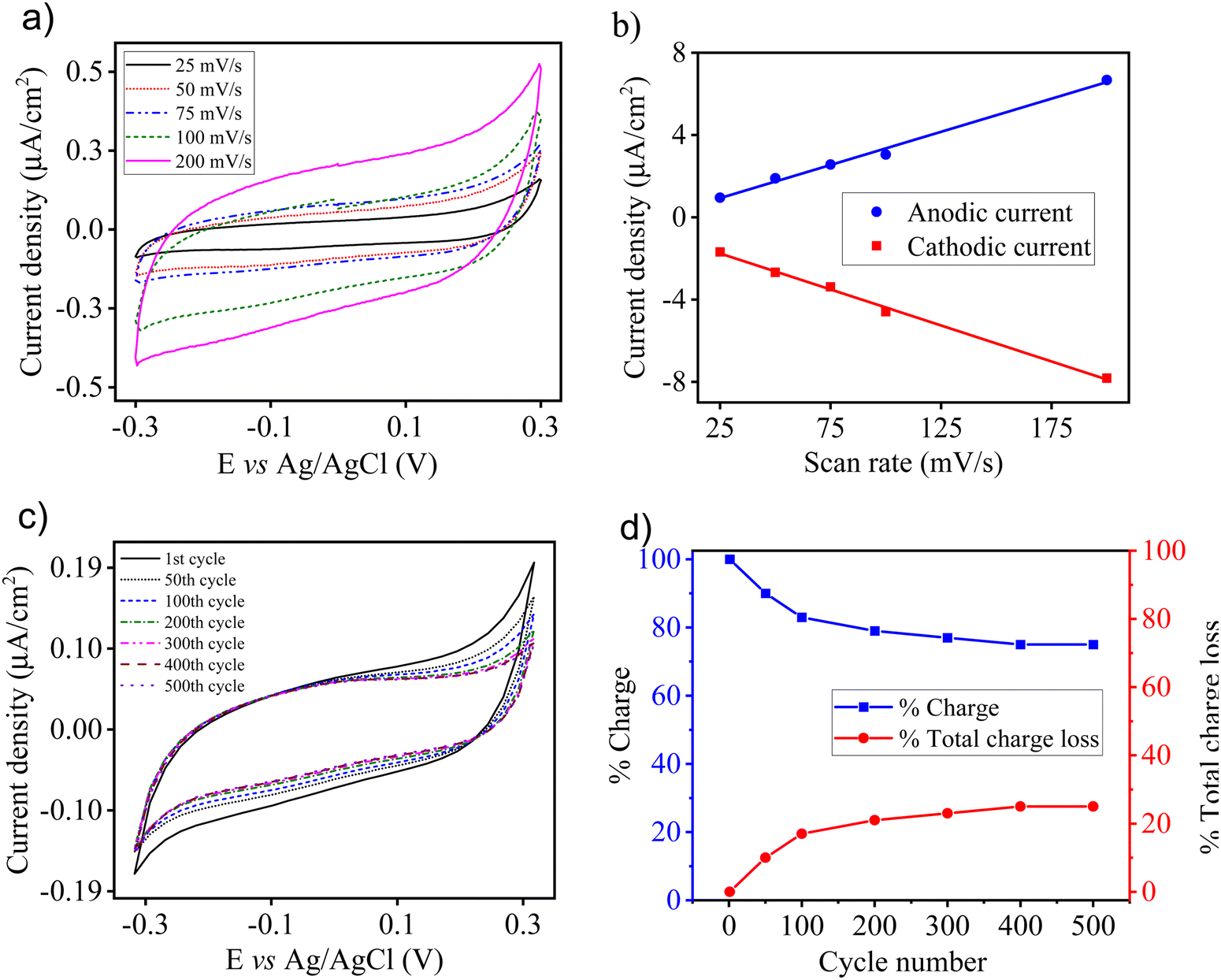
To observe the electrochemical behaviour of a thermally deposited CuSCN film, CV was carried out in DMF solution containing 0.1 M TBAClO4 as the supporting electrolyte. The CuSCN thin film was thermally deposited on a GC working electrode, and then CV was done at a potential between −0.3 and 0.3 V vs. Ag/AgCl. Fig. 3(a) represents the CV curves of a thermally deposited CuSCN film at different scan rates, which denotes the characteristic behaviour of a p-type semiconductor. In a potential range between −0.3 to 0.1 V, the CuSCN film was electrochemically inert because capacitive charging was not observed. However, at more positive potentials (between 0.1 and 0.3 V), the anodic current increased rapidly, which illustrated the charging of chemical capacitance as well as the presence of electrochemical reactions at the surface of the electrode.63,65 The voltammetry current in the region of double layer capacitance (0.1 V) of the CuSCN film was linearly dependent on the scan rate (Fig. 2(b)), which confirmed capacitive charging. The integral charges for cathodic and anodic waves were similar for each voltammogram, which displayed charge reversibility. These features showed the well-defined electrochemical properties of a thermally deposited CuSCN film in an electrochemical window of −0.3 to 0.3 V, and is in excellent agreement with the electrodeposited CuSCN film reported elsewhere.66 Outside this electrochemical window, the CuSCN film was prone to exhibit chemical and structural changes (e.g., anodic breakdown). Fig. S2a (ESI†) shows the oxidation of molecules in solution with well-defined anodic and cathodic peaks. The maximum oxidation potential peak was obtained at 0.94 V.
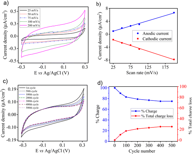 |
| | Fig. 3 (a) CV curves of thermally deposited CuSCN on a GC electrode at different scan rates in DMF solution. (b) Plot of current density versus scan rate. (c) Electrochemical stability curve of a CuSCN film on GC at a scan rate of 100 mV s−1. (d) Double Y-axis plot of % charge and % charge loss during 500 cycles. | |
Further, the electrochemical stability of thermally deposited CuSCN on the GC electrode was checked by repetitive cycling between negative and positive potentials in the potential range −0.3 to 0.3 V at a scan rate of 100 mV s−1 (Fig. 3(c)). Most charge loss occurred in the initial 100 cycles (between the 1st and 100th cycle), which was ∼17%. Only ∼2% loss of charge occurred between the 300th and 500th cycle (200 cycles), as illustrated in Fig. 3(d). The percentage charge loss was estimated and is noted in Table S1 (ESI†). These outcomes suggested that the CuSCN film became more stable with an increase in the number of redox cycles. Thus, we can infer that the CuSCN film was stable after repeated cycles, which ensured the high electrochemical stability of thermally deposited CuSCN film on GC. Upon repetitive cycling in the potential range of −0.7 to 1.3 V, the intensity of anodic and cathodic peaks decreased, which indicated dissolution of the film in DMF solution (Fig. S2b, ESI†). Upon prolonged repeated cycling, for example, at the 200th cycle, both the oxidation and reduction peaks almost disappeared.
Optical properties
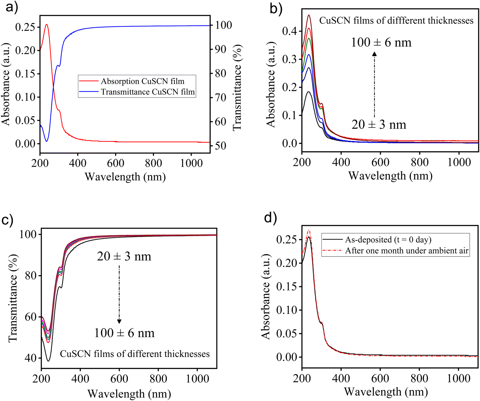
The optical transparency of the HTL is an important parameter in inverted perovskite solar cells. The absorption and transmission spectrum of a ∼30 nm thick thermally-deposited CuSCN film on a quartz substrate is represented in Fig. 4(a). The absorption spectrum showed peaks at 236 and 301 nm and absorption onset at ∼360 nm along with a long tail in the visible and NIR regions. The absorption spectrum of thermally deposited CuSCN was well-matched with the reported spectra of solution-processed CuSCN.67 Next, the transmittance spectra of a thermally deposited CuSCN film exhibited remarkably high optical transparency (> 98%) in the entire visible region. To fully explore the role of different thicknesses of a thermally deposited CuSCN film upon optical properties, UV-visible spectroscopy was carried out. Fig. 4(b) and (c) shows the absorption and transmittance spectra of thermally deposited CuSCN films on quartz substrates at various thicknesses. The absorption of the CuSCN film increased with an increase in the thickness of films. Accordingly, we obtained the maximum absorption for ∼100 nm thick CuSCN film and minimum for ∼20 nm thin film (Fig. 4(b)). On the other hand, the thermally deposited CuSCN film showed excellent transmittance in the visible–NIR region even when the thickness increased from ∼20 to 100 nm. In contrast, in the wavelength range of 200–380 nm, a reduction in the transmittance intensity of CuSCN films was observed with the increase in the thickness (Fig. 4(c)). The high transparency of CuSCN films in the visible range facilitated the maximum absorption of light by the perovskite absorber layer to generate a large amount of photocurrent, which is essential for the high performance of inverted perovskite solar cells.
 |
| | Fig. 4 (a) UV-visible absorption and transmittance spectra of a thermally deposited CuSCN thin film (∼30 nm) on a quartz substrate. (b) Absorption spectra of thermally deposited CuSCN films at various thicknesses. (c) Transmission spectra of CuSCN films. (d) CuSCN film at time t = 0 day, compared with the spectrum of the same film after t = 1 month of air exposure in an ambient environment. | |
Further, the long-term optical stability of a thermally deposited CuSCN film was investigated. The absorption spectra of the as-deposited CuSCN film and after 1 month were recorded (Fig. 4(d)). Non observable change in optical absorption was found, which indicated the excellent optical stability of the thermally deposited CuSCN film. Previous investigations on the optical properties and stability of a solution-processed CuSCN film have shown a similar result, which confirmed the suitability of the thermal deposition technique for the HTL deposition in device fabrication. Moreover, to examine the absorption behaviour of the perovskite layer in the visible region, the absorbance spectra of a CH3NH3PbI3 film on a quartz substrate was recorded (Fig. S3, ESI†). The UV-visible spectrum of a perovskite film exhibited strong absorption in the visible region with a band edge at ∼780 nm, indicating an optical bandgap of 1.59 eV.68
In situ spectroelectrochemistry.
To examine the optical changes of a CuSCN film upon electrochemical treatment, in situ spectroelectrochemistry was performed. The spectroelectrochemical measurements of a thermally deposited CuSCN film on an ITO-coated glass substrate was investigated at different potentials in 0.1 M TBAClO4/DMF solution. Fig. S4 (ESI†) represents the spectroelectrochemical spectra of a CuSCN thin film obtained after applying potentials from a negative (−0.6 V) to a positive (1.5 V) value. We saw significant changes in UV-vis-NIR spectra, suggesting the influence of an applied potential on the optoelectronic properties of a CuSCN film. At the negative potential of −0.6 V, the absorption maximum peak (λmax) of the CuSCN film was recorded at 392 nm with no absorption in the NIR region. On increasing the electrochemical potential, the intensity of the absorption maximum peak λmax decreased with a marked upsurge of absorption in the NIR region. Particularly at more positive potential values (between 0 and 0.9 V), a significant decrease in λmax was noted. Further, at potential beyond 0.9 V, we observed the shift from the isosbestic point (at λ ≈648 nm), which indicated the degradation or dissolution of the CuSCN film. We noted that studies on CuSCN have not reported the spectroelectrochemistry of a CuSCN film.
Surface morphology
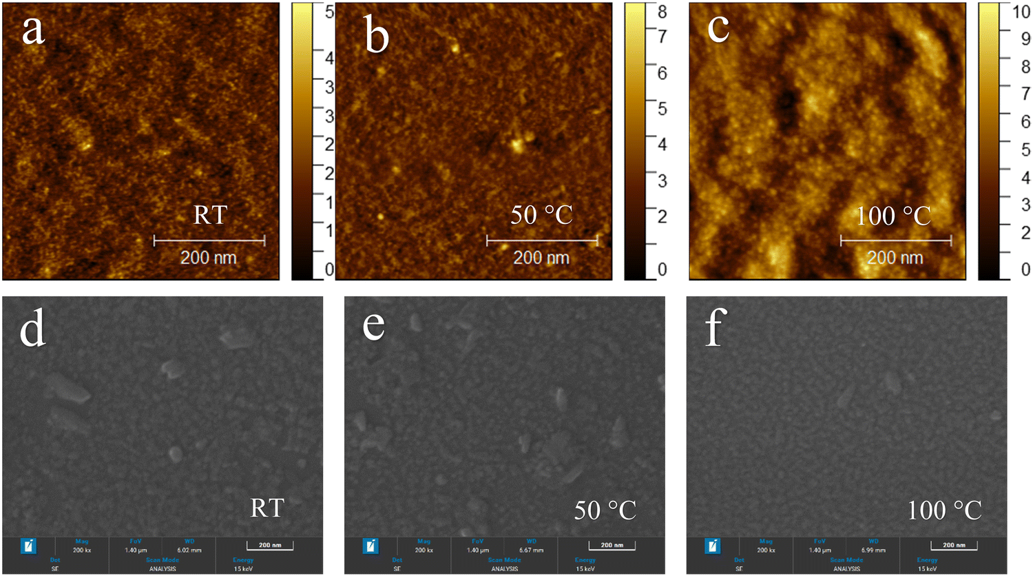
AFM and FESEM were used to study the surface morphology of thermally deposited CuSCN as HTL film in perovskite solar cells. CuSCN thin films were thermally deposited on ITO-coated glass substrates similar to those used in fabrication of perovskite devices. To examine the effect of the annealing temperature on the surface morphology of thermally deposited CuSCN, the resulting films were annealed at different temperatures (room temperature (RT), 50, 100, 150 and 200 °C) for 10 min. Fig. 5(a)–(c) represents the height images of thermally deposited CuSCN thin films at RT, 50 and 100 °C obtained from AFM measurements (0.5 × 0.5 μm2) in tapping mode. The surface root-mean-square (RMS) roughness of a CuSCN film at RT (without annealing) was 3.6 nm whereas, after being annealed at 50 and 100 °C, the CuSCN/ITO/glass exhibited a smoother surface with RMS values of 3.4 and 1.5 nm, respectively. In contrast, at higher annealing temperatures of 150 and 200 °C, the roughness of CuSCN films increased to 5.2 and 6.4 nm, respectively (Fig. S5a and b, ESI†). As a result, the CuSCN/ITO film at 100 °C (Fig. 5(c)) had a much smoother morphology (RMS ∼1.5 nm) than that of CuSCN films at other annealing temperatures. The best RMS values for spin-coated CuSCN from DES and DPS solution have been reported to be 2.58 and 2.83 nm, respectively,69 and the RMS value for electrodeposited CuSCN on ITO substrates has been reported to be 19.3 nm39 (RMS values of doctor-bladed and spray-coated CuSCN have not been reported). Thus, a comparison of the RMS value of CuSCN/ITO thin films prepared from other deposition methods and thermal deposition in this work revealed that RMS values were lower for a thermally deposited CuSCN film, which suggested that thermal deposition could be an alternative for the fabrication of smoother CuSCN thin films. The smoother surface obtained by thermal deposition is presumed to be due to the uniform film formation via the thermal deposition of CuSCN. This smoother surface can provide better contact with the ITO electrode and can aid formation of a high-quality perovskite layer.70 Furthermore, the surface coverage of CuSCN grew higher with an increase in deposition time, and the particle size showed no obvious change.
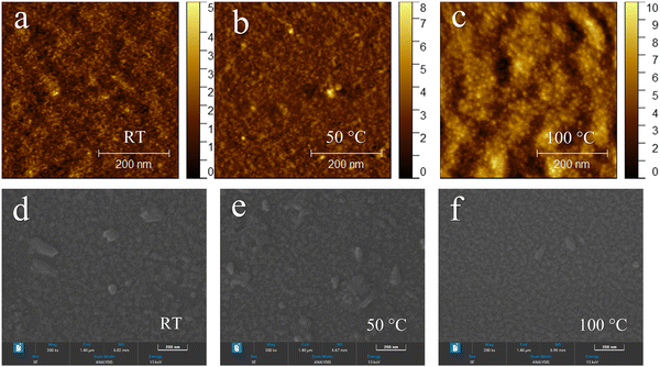 |
| | Fig. 5 (a)–(c) AFM surface topography height images (scan area of 0.5 μm2) of a thermally deposited CuSCN film on ITO-coated glass substrates with annealing temperatures of (a) RT, (b) 50 °C and (c) 100 °C. (d)–(f) FESEM images of CuSCN films at RT, 50 and 100 °C, respectively. | |
Next, the surface morphological properties of thermally deposited CuSCN films were investigated by FESEM. Fig. 5(d)–(f) display the top-view FESEM images of thermally deposited CuSCN thin films on ITO-coated glass at RT and after being annealed at 50 and 100 °C, respectively. The annealing temperature of CuSCN had an observable effect on the surface morphology. FESEM images showed a dense fine crystalline morphology of CuSCN films with well-defined orientation (Fig. 5(d)–(f)). Without annealing, the CuSCN film exhibited non-homogeneous surface coverage (Fig. 5(d)). At 100 °C, the CuSCN film had a more uniform, smoother and compact surface (Fig. 5(f)) compared with that obtained at a lower annealing temperature (Fig. 5(e)). In brief, the AFM and FESEM results of thermally deposited CuSCN thin films complemented each other (as expected), indicating the better surface morphology of the thermally deposited CuSCN thin film on the ITO surface.
Photovoltaic performance
Fig. 6(a) and (b) show the configuration of an inverted planar perovskite solar cell, and the band energy level of the materials used. p–i–n devices were fabricated using the cell configuration ITO/CuSCN/MAPbI3/PC61BM/BCP/Ag to explore the application of a thermally deposited CuSCN thin film as the HTL in perovskite solar cells. For comparison purposes, a reference cell without HTL was fabricated under similar conditions. The J–V characteristic curves of the optimized device and the reference device measured under simulated illumination (100 mW cm−2 AM 1.5) are shown in Fig. 6(c). The best performing thermally deposited CuSCN-based device exhibited an open-circuit voltage (Voc) of 1.01 V, short-circuit current density (Jsc) of 20.2 mA cm−2, and fill factor (FF) of 0.77, resulting in a maximum PCE of 15.71%. The best performance of thermally deposited CuSCN-based devices was obtained at a 30 nm thick CuSCN layer followed by annealing at 100 °C for 10 min. Under the same conditions, a device without HTL (without CuSCN) displayed a poor performance with a PCE of 5.17%, along with a significant decrease in Voc (from 1.01 V to 0.84 V), Jsc (from 20.2 mA cm−2 to 10.8 mA cm−2) and FF (from 0.77 to 0.57). A possible reason for the Jsc reduction could be attributed to the shunt path created between the perovskite layer and ITO electrode.57 Conversely, CuSCN-based devices showed high Jsc and FF due to the excellent band alignment and smooth surface morphology of the CuSCN film. Therefore, incorporating CuSCN as HTL increased the PCE by threefold along with significant enhancement in photovoltaic parameters compared with the device fabricated without HTL. The photovoltaic parameters of the reference and optimized devices are shown in Table 1. Next, to test the reproducibility of the optimized and reference devices under similar conditions, several batches of perovskite solar cells were fabricated. Fig. 6(d) represents the box chart of the photovoltaic performance of 20 devices. Devices fabricated without HTL (no CuSCN layer) showed an average PCE of 4.87% (average of 10 devices), whereas devices with CuSCN as the HTL exhibited threefold higher average PCE of 15.39% (average of 10 devices). For comparison purposes, solution-processed CuSCN-based devices were fabricated and showed a maximum PCE up to 11.89% under identical conditions (Fig. S6, ESI†).
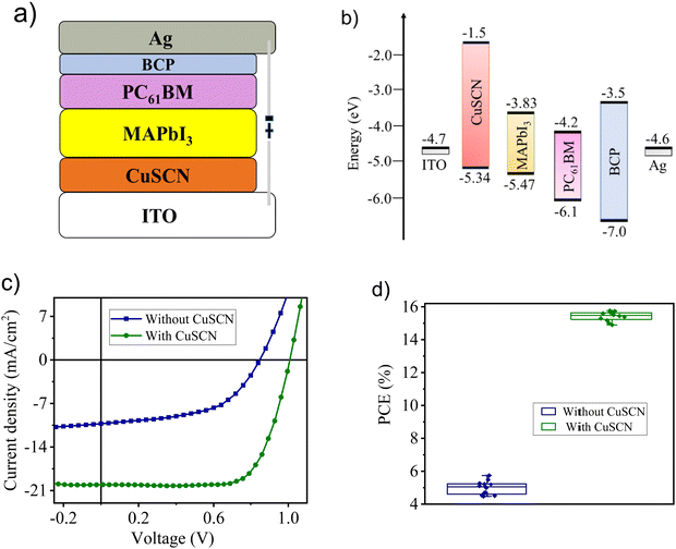 |
| | Fig. 6 (a) Block diagram of fabricated inverted planar perovskite solar cells. (b) Diagram of the corresponding band-energy level of the various materials used (relative to the vacuum level). (c) J–V characteristic curve of fabricated devices under one-sun illumination; AM 1.5 G, 100 mW cm−2. (d) Statistics of the photovoltaic performance of 20 devices. | |
Table 1 Photovoltaic parameters of inverted perovskite solar cells
| Device |
Cell configuration |
V
oc (V) |
J
sc (mA cm−2) |
FF |
PCEa (%) |
|
Champion device and in parenthesis average of 10 devices with active area of 6.0 mm2.
|
| Without HTL |
ITO/MAPbI3//PC61BM/BCP/Ag |
0.84 ± 0.02 |
10.8 ± 0.8 |
0.57 ± 0.04 |
5.17 (4.87) |
| With HTL |
ITO/CuSCN/MAPbI3/PC61BM/BCP/Ag |
1.01 ± 0.01 |
20.2 ± 0.6 |
0.77 ± 0.03 |
15.71 (15.39) |
Effect of thickness of the CuSCN layer.
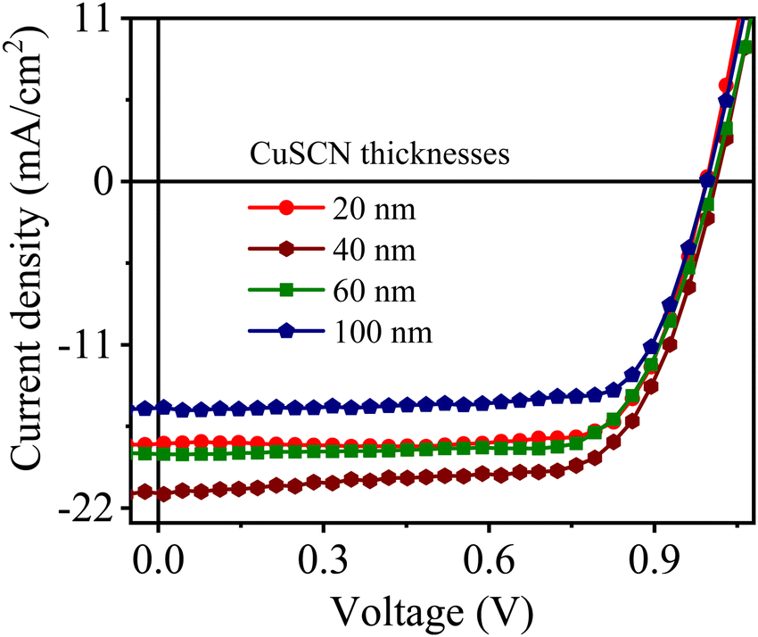
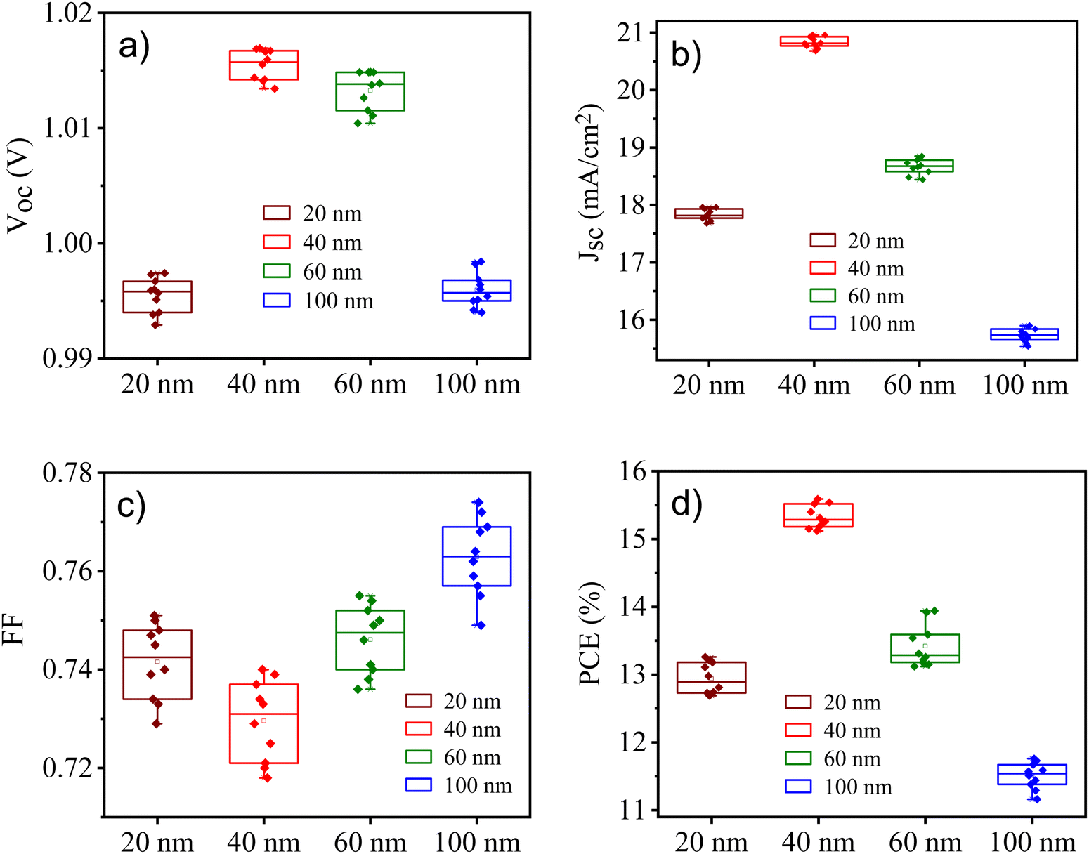
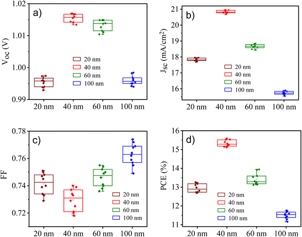
To investigate the effect of HTL thickness, we considered four thicknesses of CuSCN films: 20, 40, 60, and 100 nm. In the present work, the HTL was deposited by a thermal deposition technique in which the film thickness could be easily controlled by varying the deposition time. The thickness of each CuSCN layer was further cross-checked from the stylus profilometer. The photovoltaic performance of devices was largely dependent on the thickness of the CuSCN film as HTL. J–V characteristic curves and the parameters of their corresponding photovoltaic cells of fabricated devices using four thicknesses of CuSCN films as the HTL are presented in Fig. 7 and Table 2, respectively. When replacing a 30 nm thick CuSCN film with a thicker film or thinner film, Jsc decreased, with consistent FF and Voc values. Under identical conditions, perovskite solar cells fabricated using a 20 nm CuSCN film as HTL exhibited an average PCE of 12.95%, along with Voc = 0.99 V, Jsc = 17.7 mA cm−2 and FF = 0.74. In contrast, by increasing the thickness of CuSCN films, the efficiency of the device decreased. For example, a CuSCN film of thickness 40 nm and 60 nm showed a lower PCE of 15.08% (Voc = 1.01 V, Jsc = 20.7 mA cm−2, FF = 0.72) and 13.69% (Voc = 1.01 V, Jsc = 18.3 mA cm−2, FF = 0.74), respectively. The thickness of the HTL had an impact on the performance of the device, especially on the short-circuit current. The thickness of the HTL had a minor effect on FF, whereas there was no noticeable change in Voc. The reduced Jsc could be interpreted as a result of less efficient hole extraction and electron blocking by CuSCN films. Finally, we observed a significant decrease in PCE (from 15.71% to 11.54%) when a 100 nm thick CuSCN film was used for the fabrication of perovskite solar cells. This significant decrease was consistent and highly reproducible for several devices fabricated during this study (Fig. 8). The statistical distribution of the photovoltaic parameters extracted from 40 devices (thicknesses of 20, 40, 60, and 100 nm of the HTL were used; each thickness was used for 10 devices) based on different thicknesses of a CuSCN film is presented in Fig. 8(a)–(d). The box chart of the photovoltaic parameters (Voc, Jsc, FF and PCE) obtained from 10 devices for each thickness of the HTL showed that each thickness of CuSCN had excellent reproducibility in Voc and Jsc, along with a slight change in FF, which may have occurred during device fabrication. No significant difference in the photovoltaic performance of the device was observed. These data revealed that each thickness of CuSCN-based p–i–n perovskite solar cells was reproducible, with an average PCE of 12.95%, 15.08%, 13.69% and 11.54% obtained from CuSCN film thicknesses of 20, 40, 60, and 100 nm, respectively (Fig. 8).
 |
| | Fig. 7
J–V curves of CuSCN-based perovskite solar cells with different thicknesses of the CuSCN layer. | |
Table 2 Photovoltaic performance of CuSCN-based perovskite solar cells using various thicknesses of CuSCN films
| Thickness of CuSCN filma (nm) |
V
oc (V) |
J
sc (mA cm−2) |
FF |
PCEb (%) |
|
Thickness obtained from thermal deposition.
Average of five devices with an active area of 6.0 mm2.
|
| 20 |
0.99 ± 0.01 |
17.7 ± 0.7 |
0.74 ± 0.02 |
12.95 ± 0.80 |
| 40 |
1.01 ± 0.02 |
20.7 ± 0.5 |
0.72 ± 0.03 |
15.08 ± 0.62 |
| 60 |
1.01 ± 0.01 |
18.3 ± 0.4 |
0.74 ± 0.03 |
13.69 ± 0.53 |
| 100 |
0.99 ± 0.02 |
15.3 ± 0.6 |
0.76 ± 0.04 |
11.54 ± 0.72 |
 |
| | Fig. 8 Statistical data on (a) Voc, (b) Jsc, (c) FF and (d) PCE of CuSCN-based perovskite solar cells with different thicknesses of CuSCN films obtained from 40 devices from different batches. | |
Optimization of the annealing temperature of CuSCN.
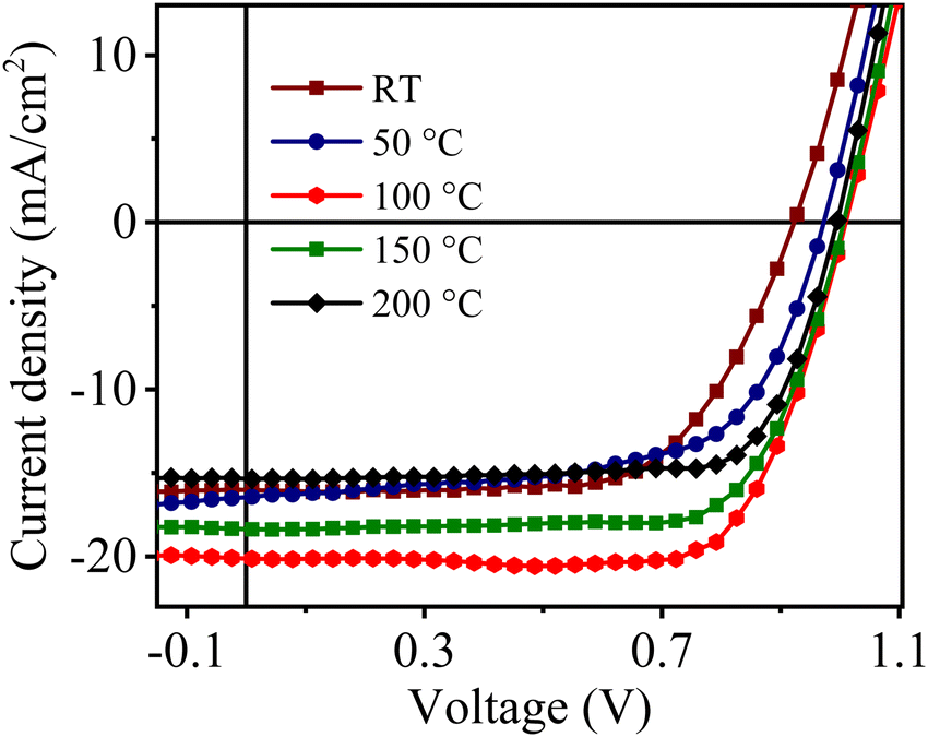
The annealing temperature of the HTL is another important parameter to reach the highest possible efficiency of a device. To investigate the influence of the annealing temperature on device performance, a 30 nm thick CuSCN film was annealed at five temperatures: RT, 50, 100, 150 and 200 °C. J–V curves were recorded under simulated illumination (AM 1.5G) in similar conditions (Fig. 9) and the corresponding photovoltaic parameters are summarized in Table 3. The device performances of the resultant perovskite solar cells were significantly affected by the annealing temperature of the CuSCN film. Without thermal treatment of a CuSCN film (RT-processed CuSCN), the resultant perovskite solar cells showed a PCE of 9.59% with a lower Voc of 0.93 V. For CuSCN films annealed at 50 °C, the resulting devices exhibited improved PCEs up to 10.18%, with enhancement in Voc from 0.93 to 0.97 V. After annealing at 100 °C for 10 min, the average efficiency was increased markedly to 15.02% with a higher Voc of 1.01 V. Further, upon increasing the annealing temperature of CuSCN films, the resulting device showed a lower device performance of 13.43% and 11.43% corresponding to annealing temperatures of 150 and 200 °C, respectively. The deteriorated performance of cells may have been due to the instability of the CuSCN film at a higher temperature, which has been reported previously.39
 |
| | Fig. 9
J–V curves of CuSCN-based perovskite solar cells with different annealing temperatures of a CuSCN film. | |
Table 3 Device parameters of CuSCN-based perovskite solar cells obtained from thermal annealing of a CuSCN film (30 nm) at different temperatures
| Annealing temperature (°C) |
V
oc (V) |
J
sc (mA cm−2) |
FF |
PCEa (%) |
|
Average of five devices with active area of 6.0 mm2.
|
| RT |
0.93 ± 0.02 |
15.4 ± 0.3 |
0.67 ± 0.03 |
9.59 ± 0.51 |
| 50 |
0.97 ± 0.02 |
16.4 ± 0.2 |
0.64 ± 0.01 |
10.18 ± 0.40 |
| 100 |
1.01 ± 0.01 |
20.1 ± 0.3 |
0.74 ± 0.02 |
15.02 ± 0.52 |
| 150 |
1.00 ± 0.02 |
18.4 ± 0.4 |
0.73 ± 0.01 |
13.43 ± 0.70 |
| 200 |
0.99 ± 0.03 |
15.4 ± 0.2 |
0.75 ± 0.02 |
11.43 ± 0.64 |
Stability studies
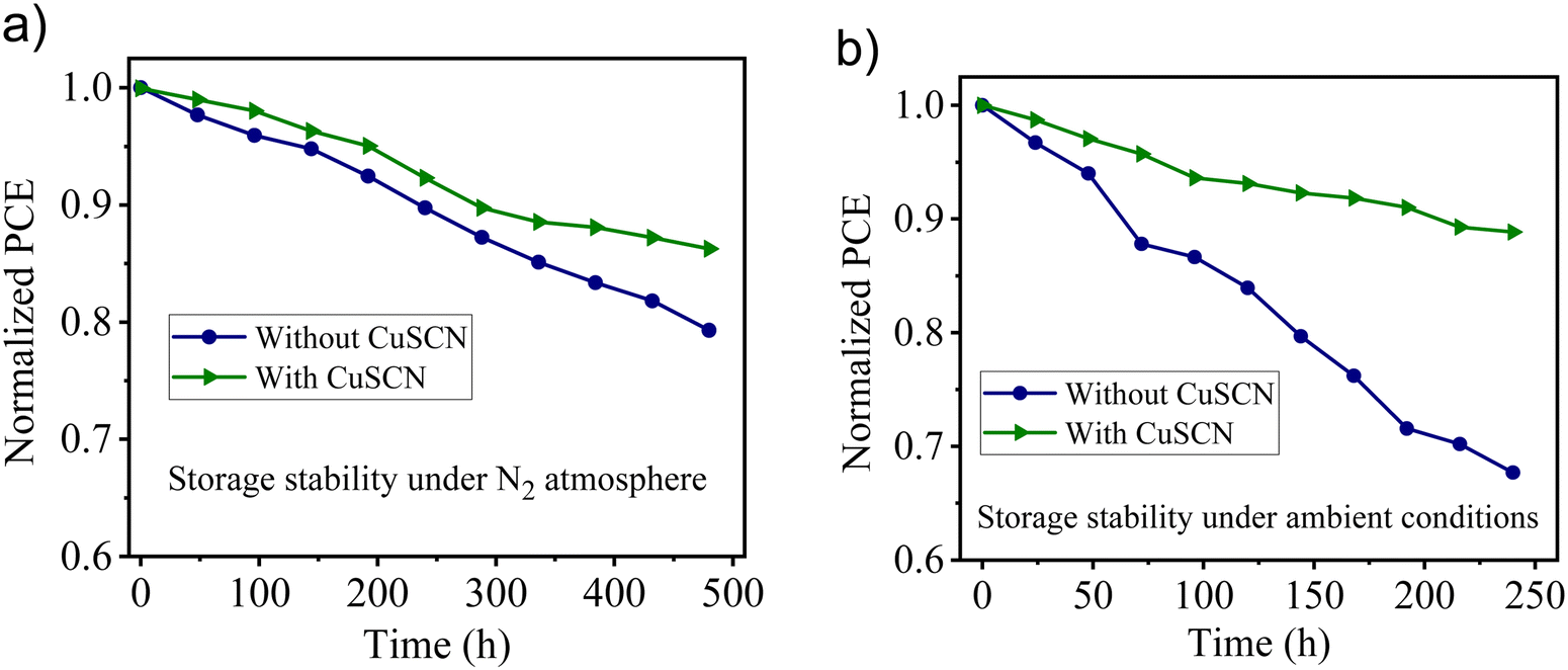
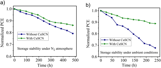
The long-term stability of cells under the N2 atmosphere as well as under ambient conditions were investigated. For the N2 atmosphere, the best-performed CuSCN (30 nm) based device without encapsulation was placed in a N2-filled glove box. The reference device (without CuSCN) was also tested under identical conditions. As a result, the thermally deposited CuSCN-based device retained ∼86% of the initial PCE after 20 days of storage in N2 atmosphere. In contrast, the reference cell showed lower stability with only ∼79% retention under identical conditions (Fig. 10(a)). Next, to study the long-term stability of cells under ambient conditions, we stored the non-encapsulated devices (with and without CuSCN-based perovskite solar cells) in the desiccator for 10 days. The CuSCN-based device showed higher long-term stability and ∼89% retention after more than 240 h (Fig. 10(b)) than without CuSCN (∼67% retention). This was in good agreement with the device performance of previously reported CuSCN-based perovskite solar cells using different deposition methods (Table 4). Thus, the excellent stability and reproducibility make it particularly attractive for low-cost commercialization. Importantly, the improvement in Jsc appeared to be independent of the atmospheric conditions under which thermal deposition of CuSCN was performed. Studies have reported similar values for Jsc and Voc for the same combination of materials,39,71 thereby making the proposed approach robust, sustainable, solvent-free and highly scalable for the fabrication of thermally deposited CuSCN-based solar cells.
 |
| | Fig. 10 Stability test of non-encapsulated devices under (a) a N2 atmosphere and (b) ambient environment. | |
Table 4 Summary of reported PCEs for various deposition methods of CuSCN-based inverted planar perovskite solar cells from the literature, and compared with the thermally deposited CuSCN approach in this work
| Deposition method |
Fabricated device |
V
oc (V) |
J
sc (mA cm−2) |
FF (%) |
PCE (%) |
Stability |
Ref. |
| Electro deposition |
ITO/CuSCN/MAPbI3/C60/BCP/Ag |
1.00 |
21.9 |
75.8 |
16.6 |
84% retention, 40 h in ambient air in dark |
38
|
| Spin coating |
ITO/CuSCN/MAPbI3/PCBM/Bis-C60/Ag |
1.07 |
19.6 |
74.0 |
16.0 |
82% retention, 300 h storage in ambient air |
39
|
| Spin coating |
ITO/CuSCN/MAPbI3/PC61BM/LiF/Ag |
1.06 |
15.2 |
64.9 |
10.8 |
40% retention, 14 days storage in N2 |
72
|
| Thermal deposition |
ITO/CuSCN/MAPbI3/PC61BM/BCP/Ag |
1.01 |
20.2 |
77.0 |
15.7 |
86% retention, 20 days storage in N2 ∼89% retention after 240 h in ambient air |
Our work |
Conclusions
For the first time, thermal deposition technique was used to prepare CuSCN thin films for HTL in inverted perovskite solar cells. The thermal deposition of CuSCN thin films was found to be an efficient, eco-friendly and alternative to solution-processable deposition of thin films. The structural characterization of thermally deposited CuSCN films was carried out by XRD analysis, Raman and FTIR spectroscopy. It was observed that CuSCN films contained only the β-phase without any impurities. The electrochemical behavior of the thermally deposited CuSCN film showed a p-type semiconductor with good electrochemical stability and capacitance. The thermally deposited CuSCN film showed high optical transparency (> 98%) in the entire visible region and long-term optical stability under ambient conditions. The thermally deposited CuSCN film exhibited a smooth surface with low RMS values and a dense, fine crystalline morphology with a well-defined orientation. The thermally deposited CuSCN film was used as HTL to fabricate inverted planar perovskite solar cells with device configuration ITO/CuSCN/MAPbI3/PC61BM/BCP/Ag. The effect of CuSCN film thicknesses and the annealing temperature of CuSCN films on the photovoltaic performance were investigated. An optimized device with a 30 nm thick CuSCN film annealed at 100 °C for 10 min exhibited the maximum PCE of 15.71% with Voc = 1.01 V, Jsc = 20.2 mA cm−2, and FF = 0.77. The thermally deposited CuSCN-based devices showed excellent reproducibility with stability up to 240 h in ambient conditions and ∼89% retention of the initial PCE. We demonstrated a new methodology for obtaining a better CuSCN film by a thermal deposition technique for efficient and scalable electronic device applications.
Conflicts of interest
There are no conflicts of interest to declare.
Acknowledgements
R. K. and M. K. acknowledge the Council of Scientific & Industrial Research (CSIR), New Delhi, India. M. B. acknowledges the University Grants Commission (UGC), New Delhi, India, for her fellowship. This work was financially supported by the TMD-DST (Sanction Order Number DST/TMD/CERI/RES/2020/12), New Delhi, India. We are thankful to Dr Naval Kishore (CSIR-NPL) for XRD characterizations and Dr Jai S. Tawale (CSIR-NPL) for the FESEM studies.
References
- Z. Yang, B. H. Babu, S. Wu, T. Liu, S. Fang, Z. Xiong, L. Han and W. Chen, Review on practical interface engineering of perovskite solar cells: From efficiency to stability, Sol. RRL, 2020, 4, 1900257 CrossRef.
- G. Shen, Q. Cai, H. Dong, X. Wen, X. Xu and C. Mu, Using interfacial contact engineering to solve nickel oxide/perovskite interface contact issues in inverted perovskite solar cells, ACS Sustainable Chem. Eng., 2021, 9, 3580–3589 CrossRef CAS.
- Z. Yang, B. Cai, B. Zhou, T. Yao, W. Yu, S. Liu, W.-H. Zhang and C. Li, An Up-Scalable Approach to CH3NH3PbI3 Compact Films for High-performance Perovskite Solar Cells, Nano Energy, 2015, 15, 670–678 CrossRef CAS.
- H. Min, D. Y. Lee, J. Kim, G. Kim, K. S. Lee, J. Kim, M. J. Paik, Y. K. Kim, K. S. Kim, M. G. Kim and T. J. Shin, Perovskite solar cells with atomically coherent interlayers on SnO2 electrodes, Nature, 2021, 598, 444–450 CrossRef CAS PubMed.
- G. M. Arumugam, S. K. Karunakaran, C. Liu, C. Zhang, F. Guo, S. Wu and Y. Mai, Inorganic hole transport layers in inverted perovskite solar cells: A review, Nano Select, 2021, 2, 1081–1116 CrossRef CAS.
- H.-S. Kim, C.-R. Lee, J.-H. Im, K.-B. Lee, T. Moehl, A. Marchioro, S.-J. Moon, R. Humphry-Baker, J.-H. Yum, J. E. Moser, M. Gratzel and N.-G. Park, Lead Iodide Perovskite Sensitized All-Solid-State Submicron Thin Film Mesoscopic Solar Cell with Efficiency Exceeding 9%, Sci. Rep., 2012, 2, 591 CrossRef PubMed.
- A. Mishra, S. Gupta and A. Patra, Synthesis and properties of 3,4-dioxythiophene and 1,4-dialkoxybenzene based copolymers via direct C–H arylation: Dopant-free hole transport material for perovskite solar cells, J. Polym. Sci., 2022, 60, 975–984 CrossRef CAS.
- J. Urieta-Mora, I. García-Benito, A. Molina-Ontoria and N. Martín, Hole Transporting Materials for Perovskite Solar Cells: A Chemical Approach, Chem. Soc. Rev., 2018, 47, 8541–8571 RSC.
- A. Krishna and A. C. Grimsdale, Hole Transporting Materials for Mesoscopic Perovskite Solar Cells - Towards A Rational Design?, J. Mater. Chem. A, 2017, 5, 16446–16466 RSC.
- Z. H. Bakr, Q. Wali, A. Fakharuddin, L. Schmidt-Mende, T. M. Brown and R. Jose, Advances in hole transport materials engineering for stable and efficient perovskite solar cells, Nano Energy, 2017, 34, 271–305 CrossRef CAS.
- A. Singh, U. K. Verma and A. Tonk, Device structures of Perovskite solar cells: A critical review, Phys. Status Solidi A, 2023, 220, 2200736 CrossRef.
- S. Mattiello, G. Lucarelli, A. Calascibetta, L. Polastri, E. Ghiglietti, S. K. Podapangi, T. M. Brown, M. Sassi and L. Beverina, Sustainable, Efficient, and Scalable Preparation of Pure and Performing Spiro-OMeTAD for Perovskite Solar Cells, ACS Sustainable Chem. Eng., 2022, 10, 4750–4757 CrossRef CAS.
- W. Han, G. Ren, J. Liu, Z. Li, H. Bao, C. Liu and W. Guo, Recent progress of inverted perovskite solar cells with a modified PEDOT:PSS hole transport layer, ACS Appl. Mater. Interfaces, 2020, 12, 49297–49322 CrossRef CAS PubMed.
- M. Yi, W. Jang and D. H. Wang, Controlled pH of PEDOT: PSS for Reproducible Efficiency in Inverted Perovskite Solar Cells: Independent of Active Area and Humidity, ACS Sustainable Chem. Eng., 2019, 7, 8245–8254 CrossRef CAS.
- M. Luo, S. Lan, X. Zong, M. Zhao, M. Hua, J. Luo and S. Xue, Novel Two-Dimensional Graphdiyne-Derived Additive for Stable Inverted Perovskite Solar Cells, ACS Sustainable Chem. Eng., 2023, 11, 3316–3323 CrossRef CAS.
- S. Naqvi, N. Chaudhary, S. Singhal, P. Yadav and A. Patra, Hole Transport Materials by Direct C-H Arylation for Organic Solar Cells: Effect of Structure and Conjugation on Electrical, Optical and Computational Properties, ChemistrySelect, 2021, 6, 131–139 CrossRef CAS.
- R. Bhargav, D. Bhardwaj, Shahjad, A. Patra and S. Chand, Poly(Styrene Sulfonate) Free Poly(3,4-Ethylenedioxythiophene) as a Robust and Solution-Processable Hole Transport Layer for Organic Solar Cells, ChemistrySelect, 2016, 1, 1347–1352 CrossRef CAS.
- S. Naqvi and A. Patra, Hole transport materials for perovskite solar cells: A computational study, Mater. Chem. Phys., 2021, 258, 123863 CrossRef CAS.
- S. Naqvi, P. Yadav, P. Pahari and A. Patra, Dodecyl-substituted poly(3,4-ethylenedioxyselenophene): polymerization and its solution-processable applications for electrochromic and organic solar cells, J. Polym. Res., 2021, 28, 250 CrossRef CAS.
- J. H. Lee, Y. W. Noh, I. S. Jin, S. H. Park and J. W. Jung, Facile surface engineering of nickel oxide thin film for enhanced power conversion efficiency of planar heterojunction perovskite solar cells, ACS Sustainable Chem. Eng., 2019, 7, 15495–15503 CrossRef CAS.
- S. Uthayaraj, D. G. B. C. Karunarathne, G. R. A. Kumara, T. Murugathas, S. Rasalingam, R. M. G. Rajapakse, P. Ravirajan and D. Velauthapillai, Powder pressed cuprous iodide (CuI) as a hole transporting material for perovskite solar cells, Materials, 2019, 12, 2037 CrossRef CAS PubMed.
- N. Chaudhary, J. Kesari, R. Chaudhary and A. Patra, Low band gap polymeric solar cells using solution-processable copper iodide as hole transporting layer, Opt. Mater., 2016, 58, 116–120 CrossRef CAS.
- Y. Zhou, C. Liu, F. Meng, C. Zhang, G. Wei, L. Gao and T. Ma, Recent progress in perovskite solar cells modified by sulfur compounds, Sol. RRL, 2021, 5, 2000713 CrossRef CAS.
- N. Chaudhary, S. Naqvi, D. Rathore, S. Rathi and A. Patra, Solvent influenced morphology control of hole transport layer of CuSCN on performance of organic solar cells, Mater. Chem. Phys., 2022, 282, 125898 CrossRef CAS.
- N. Chaudhary, R. Chaudhary, J. Kesari, A. Patra and S. Chand, Copper thiocyanate (CuSCN): an efficient solution-processable hole transporting layer in organic solar cells, J. Mater. Chem. C, 2015, 3, 11886–11892 RSC.
- N. Chaudhary, R. Chaudhary, J. P. Kesari and A. Patra, An eco-friendly and inexpensive solvent for solution processable CuSCN as a hole transporting layer in organic solar cells, Opt. Mater., 2017, 69, 367–371 CrossRef CAS.
- R. Kedia, T. Majhi, M. Balkhandia, M. Khatak, N. Chaudhary, R. K. Singh and A. Patra, Low-Temperature Aqueous Ammonia-Processed Copper(I) Selenocyanate Hole-Transporting Material for Efficient Inverted Perovskite Solar Cells, ACS Appl. Energy Mater., 2023, 6, 7091–7101 CrossRef CAS.
- S. Naqvi, N. Chaudhary, R. Kedia, P. Yadav and A. Patra, Copper(I) selenocyanate (CuSeCN): Eco-friendly solution-processable deposition of hole transport layer for organic solar cells, Sol. Energy, 2022, 231, 496–502 CrossRef CAS.
- R. Bhargav, N. Chaudhary, S. Rathi, Shahjad, D. Bhardwaj, S. Gupta and A. Patra, Copper Bromide as an Efficient Solution-Processable Hole Transport Layer for Organic Solar Cells: Effect of Solvents, ACS Omega, 2019, 4, 6028–6034 CrossRef CAS PubMed.
- A. Fakharuddin, M. Vasilopoulou, A. Soultati, M. I. Haider, J. Briscoe, V. Fotopoulos, D. Di Girolamo, D. Davazoglou, A. Chroneos, A. R. B. M. Yusoff and A. Abate, Robust inorganic hole transport materials for organic and perovskite solar cells: insights into materials electronic properties and device performance, Sol. RRL, 2021, 5, 2000555 CrossRef CAS.
- R. Singh, P. K. Singh, B. Bhattacharya and H. W. Rhee, Review of current progress in inorganic hole-transport materials for perovskite solar cells, Appl. Mater. Today, 2019, 14, 175–200 CrossRef.
- P. Pattanasattayavong, G. O. N. Ndjawa, K. Zhao, K. W. Chou, N. Yaacobi-Gross, B. C. O'Regan, A. Amassian and T. D. Anthopoulos, Electric field-induced hole transport in copper(I) thiocyanate (CuSCN) thin-films processed from solution at room temperature, Chem. Commun., 2013, 49, 4154–4156 RSC.
- J. E. Jaffe, T. C. Kaspar, T. C. Droubay, T. Varga, M. E. Bowden and G. J. Exarhos, Electronic and defect structures of CuSCN, J. Phys. Chem. C, 2010, 114, 9111–9117 CrossRef CAS.
- N. R. Paudel and Y. Yan, Application of copper thiocyanate for high open-circuit voltages of CdTe solar cells, Prog. Photovolt.: Res. Appl., 2016, 24, 94–101 CrossRef CAS.
- C. T. Tsai, S. R. Gottam, P. C. Kao, D. C. Perng and S. Y. Chu, Organic light-emitting diodes with an electro-deposited copper(I) thiocyanate (CuSCN) hole-injection layer based on aqueous electrolyte, Synth. Met., 2019, 256, 116156 CrossRef CAS.
- P. Qin, S. Tanaka, S. Ito, N. Tetreault, K. Manabe, H. Nishino, M. K. Nazeeruddin and M. Grätzel, Inorganic hole conductor-based lead halide perovskite solar cells with 12.4% conversion efficiency, Nat. Commun., 2014, 5, 3834 CrossRef CAS PubMed.
- Q. Xi, G. Gao, H. Zhou, Y. Zhao, C. Wu, L. Wang, P. Guo and J. Xu, Highly efficient inverted solar cells based on perovskite grown nanostructures mediated by CuSCN, Nanoscale, 2017, 9, 6136–6144 RSC.
- S. Ye, W. Sun, Y. Li, W. Yan, H. Peng, Z. Bian, Z. Liu and C. Huang, CuSCN-based inverted planar perovskite solar cell with an average PCE of 15.6%, Nano Lett., 2015, 15, 3723–3728 CrossRef CAS PubMed.
- J. W. Jung, C. C. Chueh and A. K.-Y. Jen, High-performance semitransparent perovskite solar cells with 10% power conversion efficiency and 25% average visible transmittance based on transparent CuSCN as the hole-transporting material, Adv. Energy Mater., 2015, 5, 1500486 CrossRef.
- I. S. Yang, M. R. Sohn, S. Do Sung, Y. J. Kim, Y. J. Yoo, J. Kim and W. I. Lee, Formation of pristine CuSCN layer by spray deposition method for efficient perovskite solar cell with extended stability, Nano Energy, 2017, 32, 414–421 CrossRef CAS.
- G. A. Sepalage, S. Meyer, A. R. Pascoe, A. D. Scully, U. Bach, Y.-B. Cheng and L. Spiccia, A facile deposition method for CuSCN: Exploring the influence of CuSCN on JV hysteresis in planar perovskite solar cells, Nano Energy, 2017, 32, 310–319 CrossRef CAS.
- G. Murugadoss, R. Thangamuthu and S. M. S. Kumar, Fabrication of CH3NH3PbI3 perovskite-based solar cells: Developing various new solvents for CuSCN hole transport material, Sol. Energy Mater. Sol. Cells, 2017, 164, 56–62 CrossRef CAS.
- V. E. Madhavan, I. Zimmermann, C. Roldan-Carmona, G. Grancini, M. Buffiere, A. Belaidi and M. K. Nazeeruddin, Copper thiocyanate inorganic hole-transporting material for high-efficiency perovskite solar cells, ACS Energy Lett., 2016, 1, 1112–1117 CrossRef CAS.
- G. R. R. A. Kumara, A. Konno, G. K. R. Senadeera, P. V. V. Jayaweera, D. B. R. A. De Silva and K. Tennakone, Dye-sensitized solar cell with the hole collector p-CuSCN deposited from a solution in n-propyl sulphide, Sol. Energy Mater. Sol. Cells, 2001, 69, 195–199 CrossRef CAS.
- Y. Yuan, G. Giri, A. L. Ayzner, A. P. Zoombelt, S. C. Mannsfeld, J. Chen, D. Nordlund, M. F. Toney, J. Huang and Z. Bao, Ultra-high mobility transparent organic thin film transistors grown by an off-centre spin-coating method, Nat. Commun., 2014, 5, 3005 CrossRef PubMed.
- L. Qiu, L. K. Ono and Y. Qi, Advances and challenges to the commercialization of organic–inorganic halide perovskite solar cell technology, Mater. Today Energy, 2018, 7, 169–189 CrossRef.
- S. S. Mali, J. V. Patil and C. K. Hong, A ‘Smart-Bottle’humidifier-assisted air-processed CuSCN inorganic hole extraction layer towards highly-efficient, large-area and thermally-stable perovskite solar cells, J. Mater. Chem. A, 2019, 7, 10246–10255 RSC.
- N. Yaacobi-Gross, N. D. Treat, P. Pattanasattayavong, H. Faber, A. K. Perumal, N. Stingelin, D. D. Bradley, P. N. Stavrinou, M. Heeney and T. D. Anthopoulos, High-Efficiency Organic Photovoltaic Cells Based on the Solution-Processable Hole Transporting Interlayer Copper Thiocyanate (CuSCN) as a Replacement for PEDOT: PSS, Adv. Energy Mater., 2015, 5, 1401529 CrossRef.
- N. Wijeyasinghe, A. Regoutz, F. Eisner, T. Du, L. Tsetseris, Y. H. Lin, H. Faber, P. Pattanasattayavong, J. Li, F. Yan and M. A. McLachlan, Copper(I) thiocyanate (CuSCN) hole-transport layers processed from aqueous precursor solutions and their application in thin-film transistors and highly efficient organic and organometal halide perovskite solar cells, Adv. Funct. Mater., 2017, 27, 1701818 CrossRef.
- N. Arora, M. I. Dar, A. Hinderhofer, N. Pellet, F. Schreiber, S. M. Zakeeruddin and M. Grätzel, Perovskite solar cells with CuSCN hole extraction layers yield stabilized efficiencies greater than 20%, Science, 2017, 358, 768–771 CrossRef CAS PubMed.
- P. Xu, J. Liu, J. Huang, F. Yu, C. H. Li and Y. X. Zheng, Interfacial engineering of CuSCN-based perovskite solar cells via PMMA interlayer toward enhanced efficiency and stability, New J. Chem., 2021, 45, 13168–13174 RSC.
- J. Sun, N. Zhang, J. Wu, W. Yang, H. He, M. Huang, Y. Zeng, X. Yang, Z. Ying, G. Qin and C. Shou, Additive Engineering of the CuSCN Hole Transport Layer for High-Performance Perovskite Semitransparent Solar Cells, ACS Appl. Mater. Interfaces, 2022, 14, 52223–52232 CrossRef CAS PubMed.
- J. W. Liang, Y. Firdaus, R. Azmi, H. Faber, D. Kaltsas, C. H. Kang, M. I. Nugraha, E. Yengel, T. K. Ng, S. De Wolf and L. Tsetseris, Cl2-Doped CuSCN Hole Transport Layer for Organic and Perovskite Solar Cells with Improved Stability, ACS Energy Lett., 2022, 7, 3139–3148 CrossRef CAS.
- Z. He, F. Meng, L. Li, L. Gao and T. Ma, Organic ammonium salt-assisted pinhole-free CuSCN films for carbon-based perovskite solar cells, New J. Chem., 2021, 45, 21382–21388 RSC.
- Y. Li, L. Meng, Y. Yang, G. Xu, Z. Hong, Q. Chen, J. You, G. Li, Y. Yang and Y. Li, High-Efficiency Robust Perovskite Solar Cells on Ultrathin Flexible Substrates, Nat. Commun., 2016, 7, 10214 CrossRef CAS PubMed.
- D. L. Smith and V. I. Saunders, The structure and polytypism of the β modification of copper(I) thiocyanate, Acta Crystallogr., Sect. B: Struct. Crystallogr. Cryst. Chem., 1981, 37, 1807–1812 CrossRef.
- I. M. Asuo, S. Bouzidi, I. Ka, F. Rosei, A. Pignolet, R. Nechache and S. G. Cloutier, All-Ambient-Processed CuSCN as an Inexpensive Alternative to Spiro-OMeTAD for Perovskite-Based Devices, Energy Technol., 2021, 9, 2000791 CrossRef CAS.
- P. Pattanasattayavong, V. Promarak and T. D. Anthopoulos, Electronic properties of copper(I) thiocyanate (CuSCN), Adv. Electron. Mater., 2017, 3, 1600378 CrossRef.
- Y. Lv, Y. Jin, W. Cai, Z. Zhang, X. Zhou and H. Chen, Air-processed carbon-based perovskite solar cells with enhanced efficiency and stability: Effect of temperature control and using CuSCN, J. Alloys Compd., 2020, 821, 153272 CrossRef CAS.
- G. R. Kumar, A. D. Savariraj, S. N. Karthick, S. Selvam, B. Balamuralitharan, H. J. Kim, K. K. Viswanathan, M. Vijaykumar and K. Prabakar, Phase transition kinetics and surface binding states of methylammonium lead iodide perovskite, Phys. Chem. Chem. Phys., 2016, 18, 7284–7292 RSC.
- J. Ding, S. Du, Y. Zhao, X. Zhang, Z. Zuo, H. Cui, X. Zhan, Y. Gu and H. Sun, High-quality inorganic–organic perovskite CH3NH3PbI3 single crystals for photo-detector applications, J. Mater. Sci., 2017, 52, 276–284 CrossRef CAS.
- L. Kavan, Z. V. Zivcova, P. Hubík, N. Arora, M. I. Dar, S. M. Zakeeruddin and M. Grätzel, Electrochemical characterization of CuSCN hole-extracting thin films for perovskite photovoltaics, ACS Appl. Energy Mater., 2019, 2, 4264–4273 CrossRef CAS.
- N. N. Shlenskaya, A. S. Tutantsev, N. A. Belich, E. A. Goodilin, M. Gratzel and A. B. Tarasov, Electrodeposition of porous CuSCN layers as hole-conducting material for perovskite solar cells, Mendeleev Commun., 2018, 28, 378–380 CrossRef CAS.
- G. A. Bowmaker and J. V. Hanna, IR Spectroscopy of Two Polymorphs of Copper(I) Thiocyanate and of Complexes of Copper(I) Thiocyanate with Thiourea and Ethylenethiourea, Z. Naturforsch. B, 2009, 64, 1478–1486 CrossRef CAS.
- Z. V. Živcová, O. Frank, V. Petrák, H. Tarábková, J. Vacík, M. Nesládek and L. Kavan, Electrochemistry and in situ Raman spectroelectrochemistry of low and high quality boron doped diamond layers in aqueous electrolyte solution, Electrochim. Acta, 2013, 87, 518–525 CrossRef.
- Z. Vlčková Živcová, M. Bouša, M. Velický, O. Frank and L. Kavan, In situ Raman microdroplet spectroelectrochemical investigation of CuSCN electrodeposited on different substrates, Nanomaterials, 2021, 11, 1256 CrossRef PubMed.
- N. Wijeyasinghe, F. Eisner, L. Tsetseris, Y. H. Lin, A. Seitkhan, J. Li, F. Yan, O. Solomeshch, N. Tessler, P. Patsalas and T. D. Anthopoulos, p-Doping of Copper(I) Thiocyanate (CuSCN) Hole-Transport Layers for High-Performance Transistors and Organic Solar Cells, Adv. Funct. Mater., 2018, 28, 1802055 CrossRef.
- P. Fan, D. Gu, G. X. Liang, J. T. Luo, J. L. Chen, Z. H. Zheng and D. P. Zhang, High-performance perovskite CH3NH3PbI3 thin films for solar cells prepared by single-source physical vapour deposition, Sci. Rep., 2016, 6, 1–9 CrossRef PubMed.
- B. Wang, S. Nam, S. Limbu, J. S. Kim, M. Riede and D. D. Bradley, Properties and Applications of Copper(I) Thiocyanate Hole-Transport Interlayers Processed from Different Solvents, Adv. Electron. Mater., 2022, 8, 2101253 CrossRef CAS.
- X. Ren, D. Yang, Z. Yang, J. Feng, X. Zhu, J. Niu, Y. Liu, W. Zhao and S. F. Liu, Solution-processed Nb:SnO2 electron transport layer for efficient planar perovskite solar cells, ACS Appl. Mater. Interfaces, 2017, 9, 2421–2429 CrossRef CAS PubMed.
- I. S. Jin, J. H. Lee, Y. W. Noh, S. H. Park and J. W. Jung, Molecular doping of CuSCN for hole transporting layers in inverted-type planar perovskite solar cells, Inorg. Chem. Front., 2019, 6, 2158–2166 RSC.
- K. Zhao, R. Munir, B. Yan, Y. Yang, T. Kim and A. Amassian, Solution-processed inorganic copper(I) thiocyanate (CuSCN) hole transporting layers for efficient p–i–n perovskite solar cells, J. Mater. Chem. A, 2015, 3, 20554–20559 RSC.
Footnote |
| † Electronic supplementary information (ESI) available: XRD patterns of CH3NH3PbI3 film. CV curve of thermally deposited CuSCN on a GC electrode in the potential range of −0.7 to 1.3 V. Electrochemical stability test of a CuSCN film on GC in the same potential window. Table of the percentage (%) charge and (%) total charge loss of a thermally deposited CuSCN film on GC. UV-visible spectrum of a perovskite film. Spectroelectrochemistry of a thermally deposited CuSCN film. AFM height images. J–V curve. See DOI: https://doi.org/10.1039/d4ya00034j |
|
| This journal is © The Royal Society of Chemistry 2024 |
Click here to see how this site uses Cookies. View our privacy policy here. 
 Open Access Article
 This Open Access Article is licensed under a
  ab,
Manisha
Balkhandia
ab,
Manisha
Khatak
ab,
Neeraj
Chaudhary
a and
Asit
Patra
ab,
Manisha
Balkhandia
ab,
Manisha
Khatak
ab,
Neeraj
Chaudhary
a and
Asit
Patra