
 Open Access Article
 This Open Access Article is licensed under a
 Creative Commons Attribution 3.0 Unported Licence
Interfacial charge doping effect in C8-DNTT/PDIF-CN2 heterojunction field-effect transistors†
Fabio
Chiarella
 *a,
Antonio
Carella
b,
Antonio
Cassinese
ac and
Mario
Barra
*a
*a,
Antonio
Carella
b,
Antonio
Cassinese
ac and
Mario
Barra
*a
aCNR-SPIN, c/o Dipartimento di Fisica “Ettore Pancini”, P.le Tecchio, 80, Naples I-80125, Italy. E-mail: fabio.chiarella@spin.cnr.it; mario.barra@spin.cnr.it
bDipartimento di Scienze Chimiche, Università degli Studi di Napoli ‘Federico II’, Complesso Universitario Monte Sant’Angelo, Via Cintia 21, I-80126, Napoli, Italy
cPhysics Department, University of Naples ‘Federico II’, P.le Tecchio, 80, Naples I-80125, Italy
First published on 17th April 2024
Abstract
In the last 15 years, DNTT-based compounds have emerged as a new generation of hole-transporting (p-type) organic semiconductors with superior charge transport properties. Even today, indeed, this class of derivatives is under intense scrutiny for the achievement of high-performance field-effect transistors to be applied in the development of advanced organic circuitry. Here, we analyze the growth of evaporated C8-DNTT films on HMDS-treated SiO2 surfaces, highlighting the dependence of the related morphological and electrical properties on the substrate temperature (Tsub) held during film condensation. In this way, we identified a Tsub range able to guarantee high mobility values (larger than 2.5 cm2 V−1 s−1) and morphological features being more compatible for the growth of additional layers on their top surfaces. This finding was the basic point to investigate the deposition of n-type PDIF-CN2 films on bottom C8-DNTT layers for the fabrication of heterojunction field-effect transistors. The electrical characterization of these devices, providing a shift of the threshold voltages and a minor sensitivity to the bias stress effect in comparison with the single-layer C8-DNTT counterparts, suggests the formation of a charge accumulation region at the organic/organic interface. This scenario was confirmed by additional electrical analyses performed on complementary double-layer structures.
Introduction
Initially introduced in the 90s, thienoacenes represent a wide class of π-extended hetero-aromatics characterized by a conjugated core where thiophene rings are combined with hydrocarbon structures (acenes) based, for their part, on linearly fused benzene rings.1,2 When compared with polyacenes, being among the most studied compounds (e.g. pentacene) within the first generation of organic semiconductors, thienoacenes exhibit generally low-lying HOMO levels and larger values of optical band gaps.Despite the interest in their potential application for innovative electronics, until the mid-2000s, devices based on thienoacenes exhibited rather limited performances. The situation rapidly changed when a specific family of thienoacenes, featuring a conjugated molecular core with two fused thiophene rings in the central part and external acenes, was demonstrated to exhibit superior charge transport properties and, consequently, a strong appeal for the fabrication of organic field-effect transistors (OFETs).3 In particular, the [1]benzothieno[3,2-b][1]benzothiophene (BTBT) molecule, when functionalized with additional terminal groups such as alkyl chains or phenyl rings, was found to provide charge carrier mobility values larger than 1 cm2 V−1 s−1, overcoming the performances of prototypical pentacene.4 In this context, it was argued that, in comparison with carbon, the larger electron densities on the sulfur atoms in the HOMO configuration could favor the effective overlap between the frontier molecular orbitals of neighboring molecules, thus enhancing the related charge transfer rate.1 BTBT-based materials are now widely investigated for the deposition of thin films,5 in particular, through solution-based techniques, achieving mobility values which, in some cases, were reported to exceed 10 cm2 V−1 s−1.6
In 2007, a π-extended BTBT analogue, called dinaphtho[2,3-b:2′,3′-f]thieno[3,2-b]thiophene (DNTT), was synthesized, revealing excellent self-assembly properties and high mobility values when evaporated in the form of thin films.7 Nowadays, DNTT is one of the most investigated hole-transporting organic compounds8–10 and is widely considered for the development of innovative devices such as environmental sensors11 and radiation detectors.12 Several studies have outlined that, owing to its large ionization potential (i.e. the HOMO level is about −5.4 eV),1 DNTT exhibits much more stable electrical performances under ambient conditions if compared with pentacene, which can be more easily oxidized (the HOMO level is about −5.0 eV).13 It was also demonstrated that even better charge transport properties can be obtained when the DNTT basic molecular core is functionalized with side alkyl chains. A detailed analysis by Kang et al.14 pointed out that the length of the alky-chains impacts the final electrical performances with the best results achievable when a decyl chain (C10-DNTT) was considered.
In evaporated films of alkyl-DNTT derivatives, molecules stand approximately upright with their longer axis being almost orthogonal to the growth surface (i.e. the conjugated plane is parallel to the substrate). Molecular packing follows a herringbone motif providing an almost isotropic charge transport within any monolayer. This feature is related to the specific molecular arrangement which gives rise to similarly large intermolecular overlaps of the π-orbitals in all the different planar directions.9 The peculiar 2D character of the charge transport in these compounds is also beneficially combined with the reduction of the dynamic disorder, associated with intermolecular thermal vibrations having lower amplitudes in comparison with alternative conjugated molecules.15
Even today, C10-DNTT is the compound of this family with the reported best charge transport performances and charge carrier mobility approaching 10 cm2 V−1 s−1.16 These outstanding properties motivated several studies about the growth mode of this compound when evaporated from effusive Knudsen cells on various types of substrates. Hence, it was shown that, along with their superior electrical features, C10-DNTT films display specific morphological properties and the characteristic presence of very tall (up to hundreds of nanometers) lamellae protruding from the underneath surface.16 It has also been clarified that these features are strongly correlated with the temperature of the substrate (Tsub) held during film deposition. When Tsub is increased and overcomes a certain range (well above 100 °C), the lamellae density is strongly reduced and the basic 2D-like film structure with flat surfaces tends to emerge with much more clarity. For C10-DNTT, however, this effect is also accompanied by a worsened connectivity of the crystalline grains and the related mobility values get considerably lowered.16
In comparison with C10-DNTT and other DNTT-based molecules bearing biphenyl side chains,17 the growth by evaporation of the dioctyl-DNTT (C8-DNTT) derivative (see Fig. S1 in the ESI† for the molecular structure and the HOMO–LUMO levels) has been much less explored and very few studies are presently available.18 Although this compound was reported to exhibit lower mobility values in comparison with C10-DNTT, it was recently investigated in terms of its thermal transport characteristics, demonstrating suppressed thermal conductivity in comparison with the parent DNTT molecule. This behavior was explained by invoking the strong localization of the intermolecular vibrational modes induced by the presence of the alky side chains.19 Among others, this observation aroused new interest for this compound in view of its possible application in thermoelectric devices.
In this work, we carefully analyzed the growth of C8-DNTT films on SiO2 substrates functionalized with hexamethyldisilazane (HMDS). Similar to that reported for C10-DNTT,16 we identified the temperature range between 60 and 90 °C for Tsub as the most promising to obtain large charge carrier mobility values. When Tsub was fixed at 85 °C, moreover, the film surface appears flatter, and the occurrence of the protruding 3D lamellae is noticeably attenuated. Starting from these findings, we investigated the response of double-layer active channels consisting of N,N′-1H,1H-perfluorobutyl-1,6-dicyanoperylene-3,4:9,10-bis(dicarboximide) (PDIF-CN2) (Fig. S1, ESI†) layers grown with different thicknesses on pre-deposited 15 nm thick C8-DNTT films. PDIF-CN2 is still today one of the most widely investigated compounds because of its remarkable air-stable electron-transporting features.20
As a whole, the electrical analysis of the final heterojunction transistors suggests that, although the combination of PDIF-CN2 and C8-DNTT does not provide field-effect devices with a balanced ambipolar response, it allows the achievement of an interfacial charge accumulation region producing a clear shift of the threshold voltages for the hole-transporting channel and a significantly reduced sensitivity to the bias stress phenomenon in comparison with the single-layer devices. More evidence about the formation of a conducting interface between C8-DNTT and PDIF-CN2 was obtained by analyzing the response of double-layer channels deposited on glass substrates and field-effect transistors relying on the inverted PDIF-CN2/C8-DNTT configuration.
Experimental
C8-DNTT and PDIF-CN2 (ActivInk N1200) were purchased from LUMTEC and FLEXTERRA, respectively, and used without any further purification. Film evaporation was carried out in a high vacuum (P ∼ 10−7 mbar) by Knudsen cells with evaporation rates ranging between 0.4 and 0.5 nm min−1 for both compounds. The substrate temperature (Tsub) was set in the range between 25 and 100 °C according to the specific experiment. For the fabrication of bottom-contact transistors, the organic films were evaporated on substrates consisting of a 500-μm-thick highly doped silicon (Si++) layer, working also as the gate electrode, a 200-nm-thick SiO2 dielectric barrier and pre-patterned gold electrodes with an interdigitated layout.21 For top-contact field-effect devices, similar Si++/SiO2 substrates, without pre-patterned contacts, were utilized. In this case, after the organic film deposition, the devices were completed through the evaporation using a shadow mask of gold rectangular pads acting as source/drain electrodes (P ∼ 10−5 mbar, a deposition rate of about 2 nm s−1, and a final thickness of 40 nm). The same top-contact configuration was employed to perform current–voltage (IV) measurements with the organic layers being evaporated on glass substrates. For all the tested samples, before the organics’ deposition, the growth surface was cleaned and made more hydrophobic by applying HMDS self-assembling monolayers following a previously optimized protocol.22 The morphological features of the film surface were analyzed by atomic force microscopy (AFM) carried out using a XE-100 Park atomic force microscope, equipped with silicon-doped cantilevers (resonance frequency around 300 KHz) provided by Nanosensor™. AFM images were acquired at a resolution of 512 × 512 pixels. Film thickness values were monitored in situ using a quartz microbalance and checked ex situ by AFM. The electrical tests were performed in a vacuum (P ∼ 10−5 mbar) by means of a cryogenic probe station connected to a Keithley 4200 semiconductor parameter analyzer.The field-effect mobility (μ) and threshold voltage (Vth) values were estimated by appropriately fitting the transfer-curves using the standard MOSFET equations in the linear and saturation regimes, being, respectively:
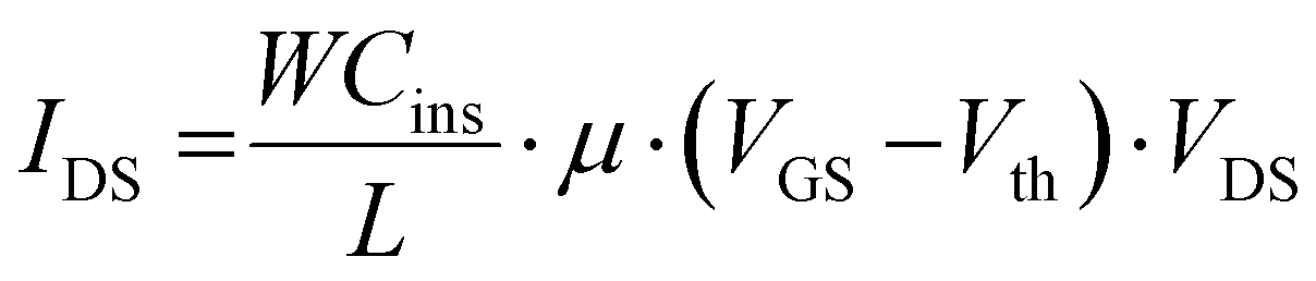 | (1) |
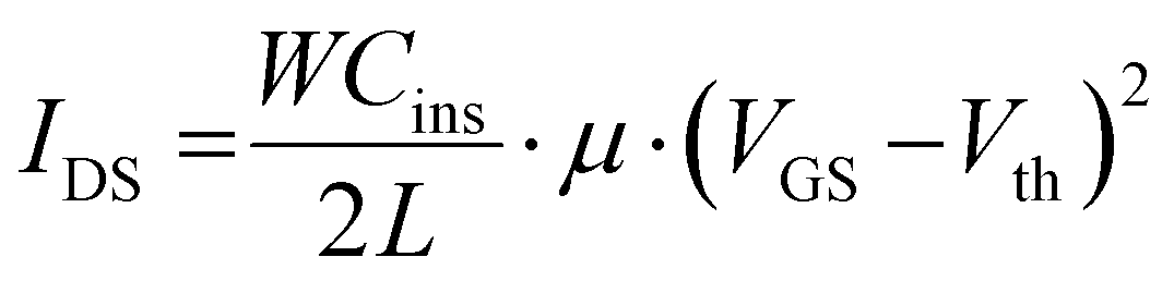 | (2) |
Here, Cins is the dielectric capacitance per unit area, being 17.3 nF cm−2 for all the considered samples, while VDS and VGS are the voltages applied, respectively, between the drain and source and the gate and source. For bottom-contact devices based on photo-lithographically patterned gold electrodes, the channel width (W) and channel length (L) were 22 mm and 40 μm (W/L ∼ 500), respectively. For the top-contact samples bearing gold electrodes achieved by shadow masks, active channels with L = 200, 150, 100 and 50 μm were fabricated, while W was invariably fixed at 500 μm. To avoid current overestimations related to the fringe effects, the active area of all the devices was carefully isolated from the remaining organic film by scratching with metallic tips operated under an optical microscope.
Results
C8-DNTT film deposition and characterization of the related field-effect devices
The initial part of this study was devoted to analyze the morphological properties of C8-DNTT films, deposited on the HMDS-treated SiO2 surface, by carefully tuning the substrate temperature (Tsub) held during the evaporation process. AFM images in Fig. 1(a–e) dealing with 50 nm thick films, indeed, show very clearly the Tsub relevant impact on the overall morphological organization. When the substrate is kept at room temperature, the C8-DNTT film surface is almost completely covered by tall lamellar structures with heights overcoming 100 nm. This specific type of nanoscale features, which make quite challenging the acquisition of clear AFM images, was also observed for C10-DNTT and diphenyl-DNTT (DPh-DNTT) layers deposited by similar evaporation processes.16,17 On the other hand, when Tsub starts to increase, the overall density of lamellae tends to be reduced even if their size apparently increases. The AFM image in Fig. 1c, taken for a film grown with Tsub = 70 °C, reveals that the main axis of the lamellar structures can approach 1 μm. The further increase of Tsub towards values of 100 °C or even larger temperatures provides a still more significant lowering of the lamellae density, with the film surfaces getting flatter and flatter and the presence of rounded-shaped molecularly terraced C8-DNTT islands emerging in the AFM images (Fig. 1d). In parallel, however, it is also possible to observe the formation of large cracks corrupting the film structural integrity (Fig. 1e). Consequently, the temperature range between 80 and 90 °C was identified as the best option to obtain a trade-off between these two morphological regimes reducing the lamellae density and avoiding the formation of the fracture lines. This favorable scenario is even clearer in Fig. 1f where a 15 nm thick film grown at Tsub = 85 °C is reported, confirming the presence of circular crystalline domains with an average diameter up to several hundreds of nanometers. From these films, we could estimate the height of the molecular terraces being close to 3.4 nm (see Fig. S2, in the ESI†), in very good agreement with the values reported in previous studies.14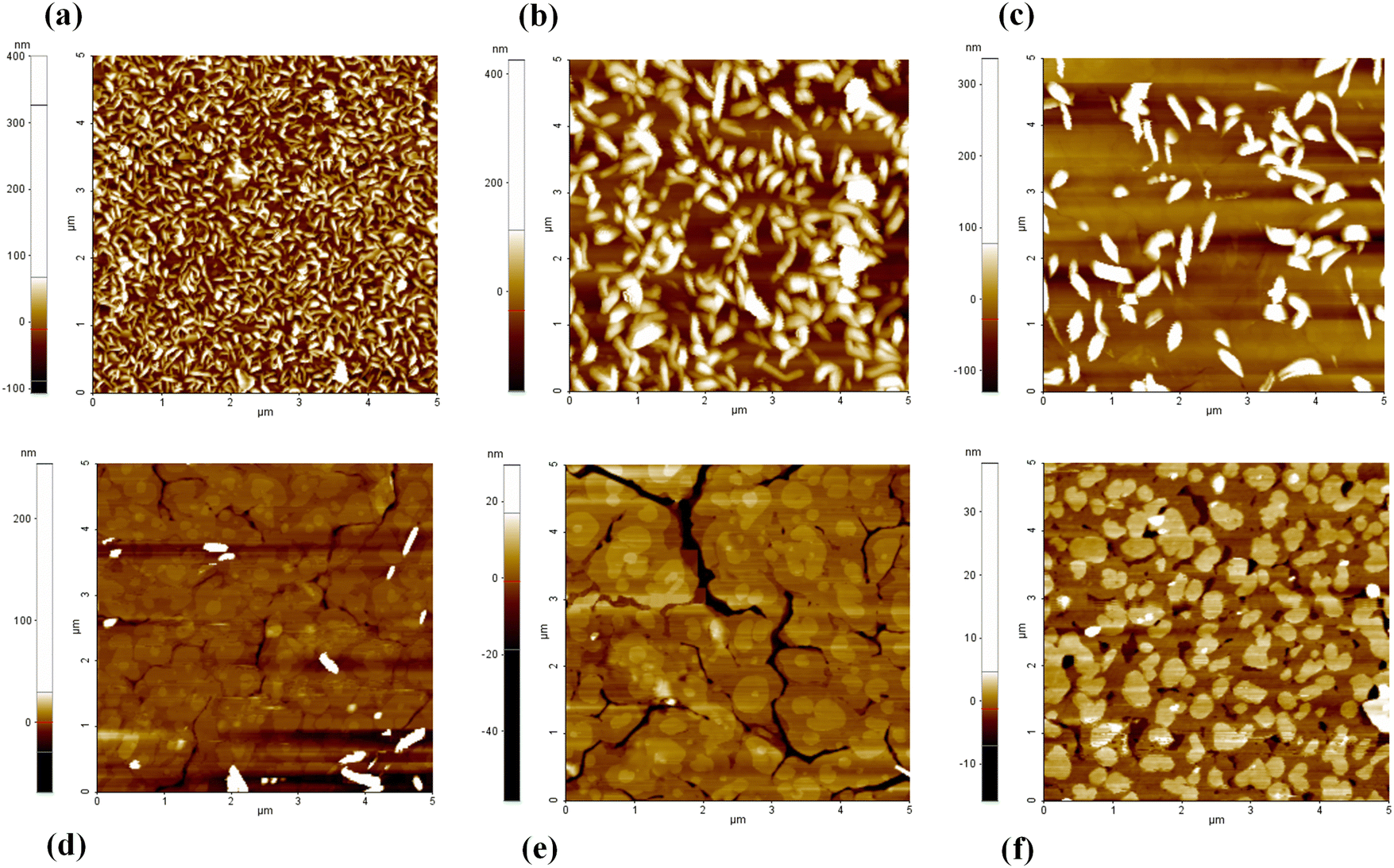 | ||
| Fig. 1 AFM images (5 × 5 μm2) of the surface of C8-DNTT films (thickness = 50 nm) deposited at different substrate temperatures (Tsub): (a) Tsub = 25 °C, (b) Tsub = 55 °C, (c) Tsub = 70 °C, (d) Tsub = 85 °C, and (e) Tsub = 100 °C. (f) Surface of a 15 nm thick C8-DNTT film deposited at Tsub = 85 °C. | ||
To check the correlation between the above discussed morphological features and the corresponding charge transport performances, bottom-contact C8-DNTT transistors, featuring active channels deposited at different Tsub, were fabricated and electrically characterized. As expected, all the analyzed devices correctly display a p-type response with the IDS current enhancement occurring at applied negative VGS (Fig. S3, in the ESI†). Significant hysteretic effects are also visible in the transfer curves and (see below for a comparison with the top-contact devices) are likely related to charge trapping phenomena mainly active in the source/drain contact regions, where the film morphology quality usually degrades for organic materials evaporated on pre-patterned metal electrodes.23,24 The maximum values of the hole mobility (μh) extracted for these devices in the saturation regime were slightly larger than 0.3 cm2 V−1 s−1, with Fig. S3c (ESI†) demonstrating that the Tsub range between 60 and 90 °C provides the best electrical performances. Conversely, mobility values turn out to be remarkably lowered when Tsub approaches 100 °C and this last behavior can be obviously ascribed to the increased presence of macroscopic fractures affecting the connectivity level between the different crystalline domains (Fig. 1e).
Based on the previous analyses, our attention was then focused on the fabrication of C8-DNTT single-layer devices bearing active layers deposited at Tsub = 85 °C and completed with 40 nm thick gold electrodes evaporated on their surfaces (i.e. top-contact configuration). Typical output and transfer-curves of this class of transistors are reported in Fig. 2 and Fig. S4 (ESI†). Output curves (Fig. 2a and b and Fig. S4a and b, ESI†) show the presence of very well defined saturation regions and an almost ideal linear response (see the following sections for a more detailed discussion on the contact resistance effect) under the application of, respectively, large and low VDS. The hysteresis effects are strongly attenuated in the transfer-curves (Fig. 2c) with the final μh values ranging between 2.5 and approximately 5 cm2 V−1 s−1. Hence, these top-contact devices display mobility values which are about one order of magnitude larger than their bottom-contact counterparts and result among the largest ever reported for the C8-DNTT compound.18,25 Interestingly, when reducing the channel length (down to 50 μm), we observed a progressive increase of the mobility, with the values extracted in the saturation regime being larger and larger than those evaluated in the linear region. These features seem to suggest a favorable effect of the lateral (i.e. between the drain and source) electric field which tends to enhance the charge carrier mobility. It is also worth to outline that, as shown in Fig. 2c, the threshold voltages (Vth) are largely negative being comprised between −10 and −25 V. This occurrence is commonly explained by considering the presence of trapping states which require to be compensated before charge carriers can be accumulated in the channel.26
 | ||
| Fig. 2 Electrical response of top-contact C8-DNTT single-layer transistors with 15 nm thick active channels deposited at Tsub = 85 °C: output curves of devices with channel lengths (L) of (a) 200 and (b) 50 μm. (c) Transfer curves measured in the linear regime (VDS = −5 V) for devices with different L. (d) Mobility and threshold voltage values extracted in the linear and saturation regimes as a function of the channel length. | ||
C8-DNTT/PDIF-CN2 heterojunction devices
The possibility to combine C8-DNTT and PDIF-CN2 in the development of p–n heterojunction-based devices posed some interesting challenges since both molecules, when evaporated in the form of thin films, are characterized by significant dependence on the deposition conditions and, more specifically, on the substrate temperature (Tsub). While the range between 80 and 90 °C was previously identified for C8-DNTT as the best option to limit the presence of the surface lamellar structures and preserve the macroscopic film integrity, several previous studies demonstrated that PDIF-CN2 films exhibit the best charge-transport performances when Tsub is set between 100 and 110 °C.27,28Hence, we tried initially to satisfy these diverse requirements by depositing sequentially the two molecules at the corresponding optimized Tsub (i.e. 85 °C for C8-DNTT and 100 °C for PDIF-CN2). As shown in Fig. S5 in the ESI,† however, this procedure affects noticeably the morphology of the C8-DNTT films which are likely subjected to a reorganization when Tsub is increased at 100 °C in view of the PDIF-CN2 deposition. These changes are directly reflected in the electrical response of the related field-effect devices showing a considerable degradation of the hole mobility (μh) which was reduced to about 0.5 cm2 V−1 s−1, while the electron mobility (μe) values in the PDIF-CN2 channel were lower than 10−4 cm2 V−1 s−1 in any case. Given these findings, a different strategy was considered, and both films were sequentially deposited while keeping the substrate temperature at 85 °C, thus reducing also the time required for the overall evaporation process. Fig. 3 shows the morphology of a few films achieved in this way, where the C8-DNTT thickness was fixed at 15 nm and that of PDIF-CN2 was varied from 10 (b–c) to 20 nm (e–f). By exploiting the shadow effect related to the use of a metallic mask to confine the organic layer mainly in the central part of the substrates, for the various samples, we were able to observe the morphology of C8-DNTT films on HMDS-SiO2 and that of the PDIF-CN2 layers grown on both HMDS-SiO2 and C8-DNTT surfaces. From these images, we can still recognize the above discussed morphology of the C8-DNTT layers, featuring well-defined circular-shaped islands and average roughness (σr) slightly higher than 3 nm, while PDIF-CN2 is characterized by the typical compact organization given by the coalescence of smaller rounded crystallites.27
 | ||
| Fig. 3 AFM images (5 × 5 μm2): (a) and (d) surfaces of 15 nm thick C8-DNTT layers grown on HMDS-treated SiO2, (b) and (e) surfaces of PDIF-CN2 films with thicknesses of 10 nm and 20 nm, respectively, grown on HMDS-treated SiO2, and (c) and (f) surfaces of PDIF-CN2 films, with thicknesses of 10 nm and 20 nm, respectively, grown on C8-DNTT bottom layers. All layers were deposited with a Tsub of 85 °C. | ||
Significantly, the PDIF-CN2 morphology on C8-DNTT is maintained even with an enhanced σr which becomes larger at increasing thickness (δF). While on HMDS/SiO2, the PDIF-CN2 film roughness is about 2.5 nm for all the investigated thicknesses, the perylene layers on C8-DNTT result much rougher with σr exceeding 5 nm when δF = 30 nm. This phenomenon resembles that recently observed for PDIF-CN2 films grown on P3HT bottom layers.29
C8-DNTT/PDIF-CN2 heterojunction transistors, fabricated according to the aforementioned protocol (Tsub = 85 °C) and with different thicknesses (δF) of the PDIF-CN2 top layer deposited on the 15 nm thick C8-DNTT bottom film, were electrically tested to assess the possibility to accumulate both holes and electrons. Typical responses of these devices in the hole accumulation regions (i.e. under the application of negative VGS and VDS) are reported in Fig. 4 and Fig. S6 (ESI†).
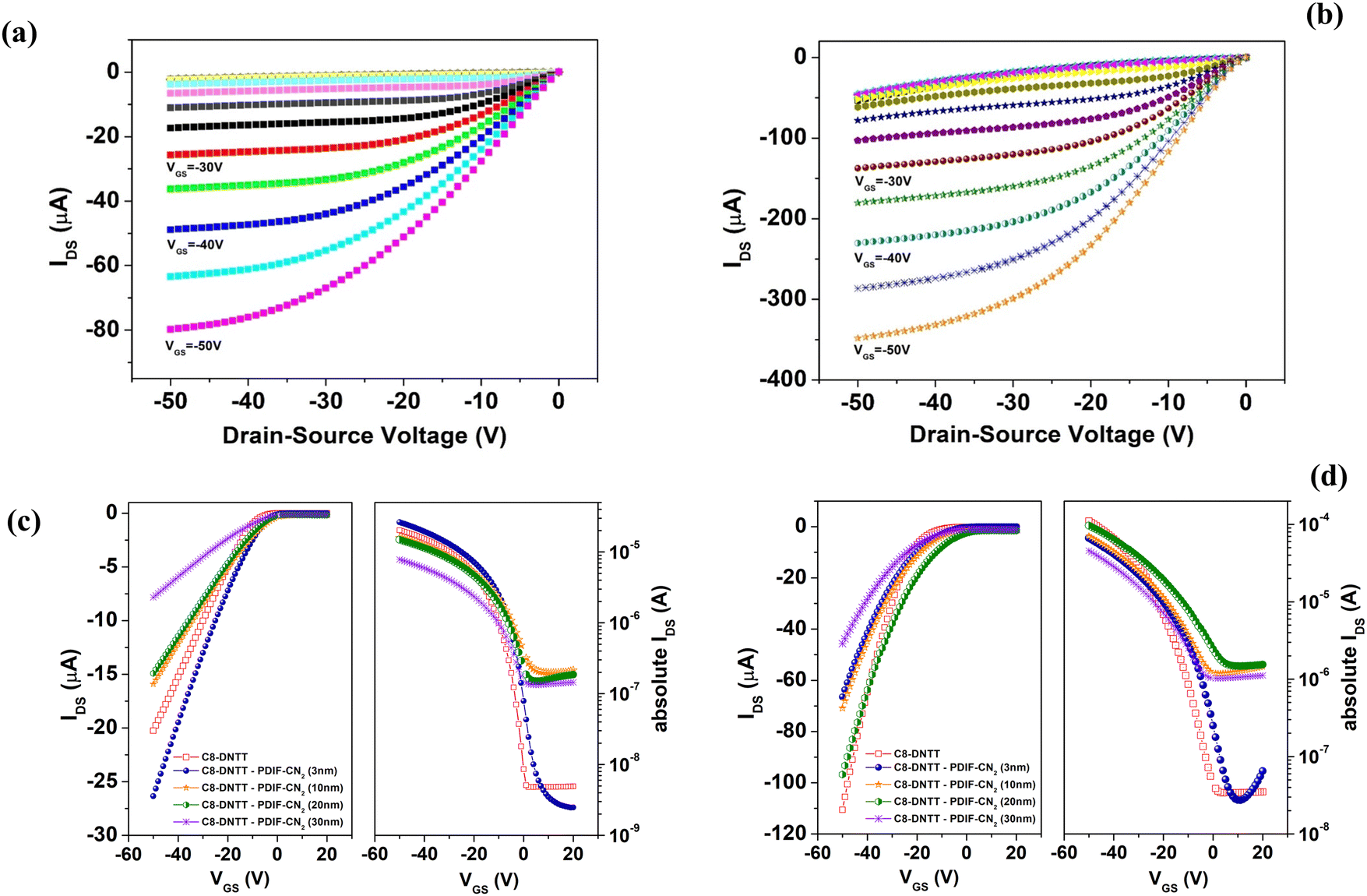 | ||
| Fig. 4 Electrical response of top-contact C8-DNTT/PDIF-CN2 heterojunction transistors in the hole accumulation region: output curves of C8-DNTT (15 nm)/PDIF-CN2 (20 nm) heterojunction transistors with active channels deposited at Tsub = 85 °C and channel lengths of (a) L = 200 and (b) 50 μm. Transfer-curves in linear and semi-log plots of C8-DNTT/PDIF-CN2 heterojunction transistors (L = 200 μm), with different thicknesses (δF) of the PDIF-CN2 top layer, measured in the (c) linear (VDS = −5 V) and (d) saturation regions (VDS = −50 V). | ||
Output curves (Fig. 4a and b and S6a (ESI†), measured with VGS ranging between +20 and −50 V) resemble those achieved with C8-DNTT single-layer devices unless the presence of non-negligible IDS currents recorded for positive VGS. This feature is more clearly shown in Fig. S6b (ESI†), where a set of output curves, measured for VGS going from +20 V and −10 V, is reported. For large negative VDS, we can notice here that the IDS current decreases (in absolute value) when VGS goes from +20 V to 0 V, while it raises again for VGS = −10 V. For positive VGS, indeed, the current flowing across the channel is dominated by electrons (negative charges) injected from the drain electrode, where the voltage difference with the gate (VGD) becomes largely positive. When VGS assumes more negative values, conversely, the hole accumulation channel is restored, and the IDS current is given only by the flow of holes injected form the source electrode. In a complementary way, output curves in Fig. S7a and b (ESI†) are recorded for positive VDS and VGS ranging from 0 to +70 V. In this case, the response (Fig. S7a, ESI†) appears ruled by the injection of holes from the drain electrode providing the typical power dependence of IDS on VDS. The electron accumulation effect is obtained only when VGS overcomes +50 V with the progressive increase of IDS up to VGS = +70 V (Fig. S7b, ESI†). The above discussed output curves clarify that the C8-DNTT/PDIF-CN2 heterojunction transistors are characterized by a strongly unbalanced ambipolar response with the hole-transporting channel being much more effective than the electron-transporting counterpart. This scenario is still more evident when the transfer-curves are considered. Fig. 4c and d report a set of transfer-curves measured, respectively, in the linear (VDS = −5 V) and saturation (VDS = −50 V) regimes of the hole accumulation region. More specifically, these data compare the behavior of a C8-DNTT single layer device with that of C8-DNTT/PDIF-CN2 heterojunction transistors having different thicknesses (δF) of the top layer (from 3 to 30 nm). For all these curves, the p-type response (i.e. hole accumulation effect) is visible well and the hole mobility values retain large values (see the discussion below). Moreover, we observe an evident enhancement (by about two orders of magnitude) of the IDS current for positive VGS when δF is larger than 10 nm.
For the sake of completeness, Fig. S7c (ESI†) reports two transfer–curves measured in the electron accumulation region under an application of VDS = +50 V. As discussed for the output curves in Fig. S7b (ESI†), the electron accumulation and the associated increase of the IDS current take place only when VGS exceeds +50 V. In this case, the VGS-driven overall percentage variation of IDS is only 10–20% in comparison with the minimum value. For the C8-DNTT/PDIF-CN2 transistors investigated in this study, no electron accumulation effect was observed for the devices with the thinnest (δF = 3 nm) PDIF-CN2 films. Conversely (see Fig. S7d, ESI†), the electron mobility (μe) values were found to be comparable for the devices with δF equal to 10 and 20 nm, remaining, in any case, mainly comprised between 10−3 and 10−2 cm2 V−1 s−1. A further μe reduction was finally observed for the C8-DNTT/PDIF-CN2 devices having δF = 30 nm. This finding should be basically associated with the enhanced 3D morphological character of the thicker PDIF-CN2 films evaporated on C8-DNTT. This occurrence is translated in a worse connection degree between the crystalline domains and a larger access resistance effect toward the organic/organic interfacial regions where electrons are accumulated.
Ascertained the prevailing p-type response of the C8-DNTT/PDIF-CN2 devices, most efforts were carried out to extract the μh and Vth values associated with the hole transport region with the specific goal (see also the Discussion and conclusions section) to analyze the related dependence on the PDIF-CN2 thickness (δF). The overall analysis is summarized in Fig. 5 where the electrical parameters, estimated in both the linear and saturation regimes, are separately plotted as a function of the device channel length (L). In general, μh values for the heterojunction devices tend to be reduced in comparison with the C8-DNTT single-layer transistors. The largest μh values are 1.5 cm2 V−1 s−1 being further lowered down to about 1 cm2 V−1 s−1 when the PDIF-CN2 thickness is increased at 30 nm. On the other hand, threshold voltages (Vth) for the devices based on C8-DNTT/PDIF-CN2 active channels are considerably less negative with average values approaching 0 and −5 V in the saturation and linear regions, respectively. In comparison with the C8-DNTT single-layer devices, hence, we can assume an average ΔVth shift of being close to 10 V which, using the equation  , provides an increase of the charge carrier density by about 1.1 × 1012 cm−2.
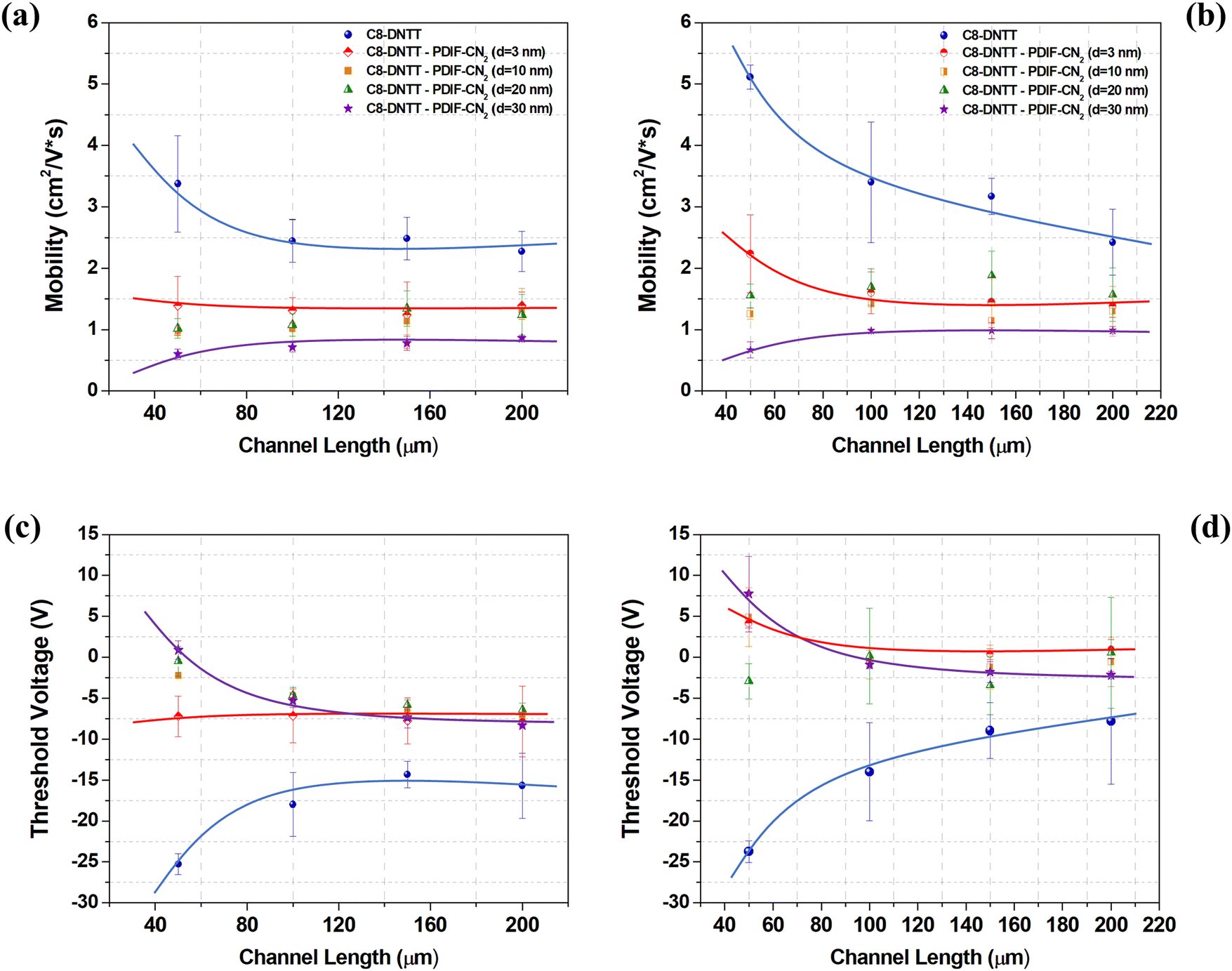 | ||
| Fig. 5 Electrical response of top-contact C8-DNTT/PDIF-CN2 heterojunction transistors with different thicknesses of the PDIF-CN2 top layer: comparison between the mobility (a) and (b) and the threshold voltage (c) and (d) values for the hole accumulation region, extracted in the linear (a) and (c) and saturation (b) and (d) regimes, as a function of the channel length. The color curves are just a guide for eyes. | ||
A further comparison between C8-DNTT single-layer and C8-DNTT/PDIF-CN2 heterojunction devices was considered in terms of the bias stress (BS) effect. This is a quite general phenomenon for OFETs, consisting of a progressive and reversible reduction of the IDS current under static voltage polarizations which drive the devices in the accumulation region. Given its importance to assess the device reliability in practical applications, this effect has been widely investigated for several organic compounds with both p- and n-type characters.30–34
Fig. 6 summarizes the results of a few experiments assessing the BS impact on the single-layer and heterojunction devices. For any analyzed transistor, we performed two consecutive BS experiments under the application of fixed polarizations (VGS = −40 V and VDS = −10 V) for 6 minutes. During the stressing periods, the IDS current was monitored continuously over the time. Transfer curves in the linear region were also recorded at the beginning of the experiment and after the two consecutive BS tests. All the data in Fig. 6 indicate that the heterojunctions are characterized by a minor sensitivity to the BS. This behavior can be observed very clearly in the IDS(t) curves (Fig. 6a and b), where the overall IDS decay factors are considerably reduced for the heterojunction transistors. As far as the first stressing period is concerned, for example, Fig. 6a shows a 30% decrease of the initial current for two different single-layer devices, while this attenuation factor is more than halved for the heterojunction ones. Coherently, in Fig. 6c, we can notice that, for a C8-DNTT/PDIF-CN2 transistor, the transfer-curves recorded after the BS periods exhibit a much minor Vth shift (about 2.5 V) if compared with the C8-DNTT single-layer counterpart where Vth becomes more negative by about 7 V. In very good agreement with the literature, the BS effect for the investigated devices impacts mainly on Vth values while producing negligible modifications of the charge carrier mobility (i.e. the IDS slope in the transfer curves).
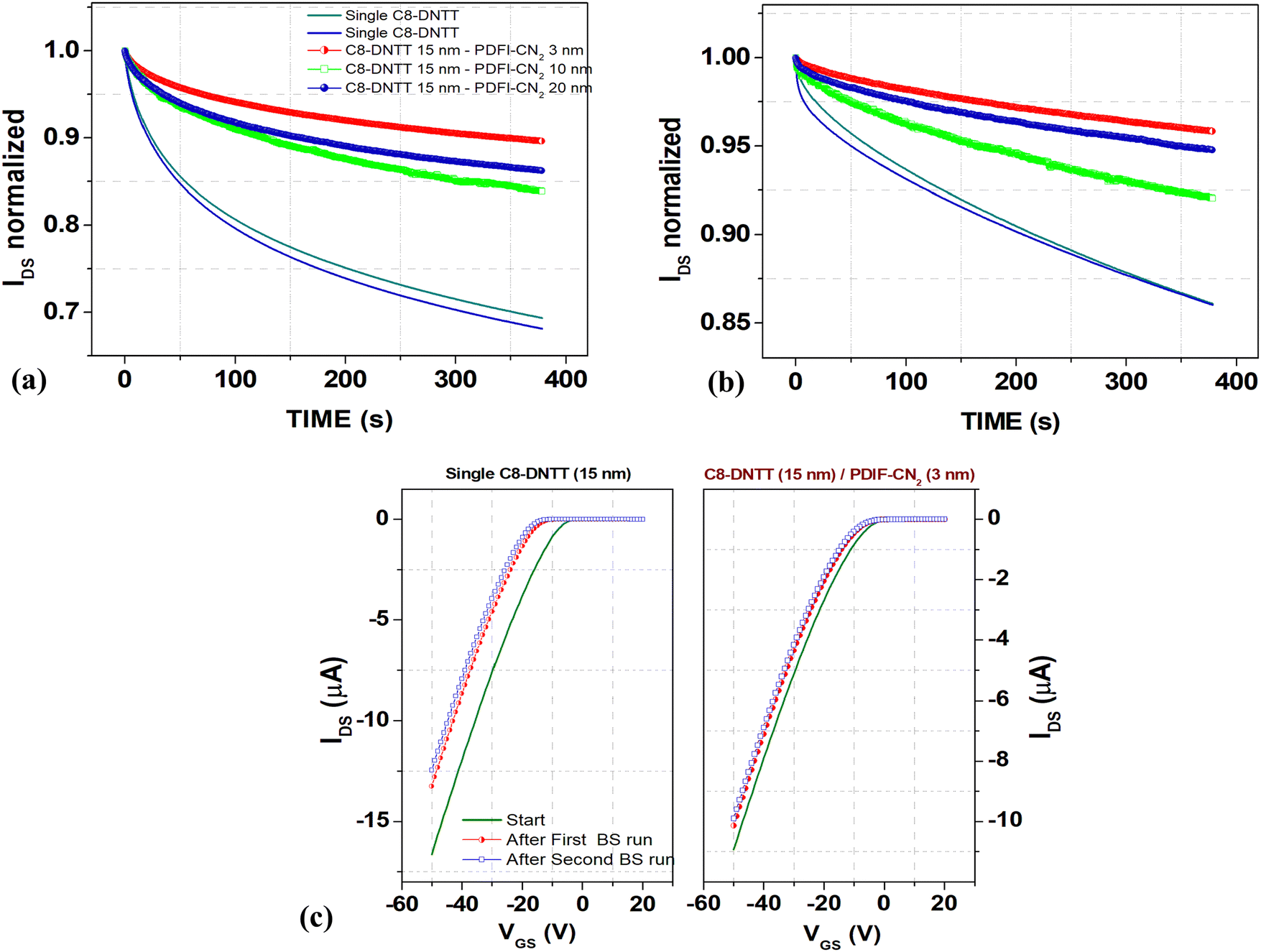 | ||
| Fig. 6 Bias stress (BS) experiments performed with C8-DNTT single-layer and C8-DNTT/PDIF-CN2 heterojunction transistors in the hole accumulation regions (VDS = −10 V and VGS = −40 V): normalized IDS current curves, as a function of the stressing time, recorded during (a) test I and (b) test II. Here, t = 0 s represents the beginning of the experiments for each run. (c) Comparison among transfer-curves measured at t = 0 s, t = 10 min (after test I), and t = 20 min (after test II) of the BS experiment. | ||
Discussion and conclusions
In summary, while analyzing the evaporation of C8-DNTT films on hydrophobic HMDS-treated SiO2 surfaces, we found that the related growth mode shows a distinctive behavior as a function of the substrate temperature (Tsub) held during deposition. We observed the presence of characteristic morphological features (i.e. protruding lamellae with a height larger than 100 nm) on the C8-DNTT film surfaces, in which the density can be significantly reduced at increasing Tsub but at the expense of the major occurrence of macroscopic structural fractures. A value of Tsub = 85 °C was found to offer a good trade-off between these two morphological regimes and related top-contact C8-DNTT single-layer devices show a p-type response with hole mobility values larger than 2.5 cm2 V−1 s−1. However, charge trapping mechanisms seem to have a non-negligible impact on the electrical behavior of these devices providing residual hysteresis effects, mobility dependence on the lateral electric field between the drain and the source, largely negative Vth threshold voltages and a certain sensitivity on the bias stress phenomenon.By exploiting the Tsub range between 80 and 90 °C to improve the flatness of C8-DNTT film surfaces, p/n heterojunction field-effect devices were fabricated by sequentially depositing PDIF-CN2 layers on C8-DNTT bottom films. These double-layer transistors display a strongly unbalanced ambipolar behavior, with the hole-transporting channel exhibiting much better performances than the electron-transporting counterpart (i.e. μh is larger than μe by about three orders of magnitude).
In comparison with the C8-DNTT single-layer devices, the hole accumulation response of the C8-DNTT/PDIF-CN2 heterojunction transistors was characterized by slightly reduced mobility values but, at the same time, exhibits a beneficial shift of the threshold voltages toward less negative values and a significantly attenuated dependence on the bias stress effect. As reported in the literature for other organic systems, in general, these findings can be ascribed to the formation of an interfacial charge accumulation layer between the p and n regions, which provides an enhancement of the density of charge carriers.35–38
However, in order to gain more insights into the diverse features here described, we analyzed more carefully the evolution of the main electrical parameters evaluated for C8-DNTT/PDIF-CN2 devices with different PDIF-CN2 overlayer thicknesses (δF).
For this purpose, in Fig. 7a (top panel), we reported the contact resistance (RC) values estimated by the transmission line method (see Fig. S8, ESI†) for a set of C8-DNTT/PDIF-CN2 heterojunction transistors. The experimental data achieved for δF = 0 nm refer to C8-DNTT single-layer devices for which RC values were found to be typically ranging between 1 and 1.5 kΩ cm. When δF was increased until 10 nm, the RC values were not significantly enhanced, while, conversely, a more pronounced increase was observed for δF = 20 nm and, still with more evidence, δF = 30 nm. In the other two panels of Fig. 7a, the hole mobility (μh) and threshold voltage (Vth) values, extracted in the linear regime for C8-DNTT/PDIF-CN2 transistors with a channel length L of 200 μm, were also plotted versus δF. Our attention was focused on the electrical parameters extracted in the linear region since they could be potentially more affected by the RC effect. From Fig. 7a, we can clearly infer that, while μh and Vth values in the C8-DNTT/PDIF-CN2 devices remain almost constant when δF ranges between 3 and 20 nm, more significant variations can be observed only for δF = 30 nm. Given these findings, we conclude that the contact resistance (RC) effect impacts on the μh reduction only for the largest PDIF-CN2 thickness while it cannot be considered as the ruling factor when δF is lower.
 | ||
| Fig. 7 (a) Contact resistance values, estimated for C8-DNTT/PDIF-CN2 heterojunctions with different thicknesses of the PDIF-CN2 overlayer, are compared with the hole mobility and threshold voltage values evaluated in the linear regime for corresponding heterojunction devices with a channel length L of 200 μm. Here, the devices with δF = 0 nm represent C8-DNTT single-layer transistors. (b) A sketch of the two main charge-transporting interfaces achieved in the investigated C8-DNTT/PDIF-CN2 structures. (c) Related energy level scenarios. | ||
In the small δF range, the μh decrease should rather be associated with the complex interplay between the charge accumulation regions at SiO2/C8-DNTT and C8-DNTT/PDIF-CN2 interfaces. Similar to what discussed in ref. 36, the interaction between the gate electric field and the charge-transfer organic–organic interface, with this latter acting basically as the dopant element, makes the conduction channel more spatially distributed in the bulk of the C8-DNTT film. Hence, this phenomenon should explain the μh decrease since, in comparison with single-layer field-effect devices, the overall charge transport in the investigated heterojunctions tends to involve also the topmost molecular layers of the C8-DNTT films being characterized by more structural defects because of the characteristic 2D + 3D growth mode (Fig. 7b) and, consequently, by an increased occurrence of charge scattering phenomena.
The energy level landscape at both C8-DNTT/SiO2 and C8-DNTT/PDIF-CN2 interfaces is summarized in Fig. 7c showing how the related frontier molecular levels are bent upwards and downwards, respectively, in correspondence with the enhanced density of holes and electrons. It is also significant to outline that the charge-transfer phenomenon taking place in the C8-DNTT/PDIF-CN2 region is favoured by the band broadening of the energy levels induced by the enhanced morphological disorder. In this way, the tail states of the HOMO (C8-DNTTT) and LUMO (PDIF-CN2) levels experience a major degree of overlapping, supporting the ion-pair formation between the molecular compounds.39 Overall, the increased morphological disorder at the C8-DNTT/PDIF-CN2 interface seems to favour the generation of charge carriers but, contemporarily, reduces the mobility performances referred to both holes and electrons.
In phenomenological terms, the μh reduction here observed for small δF resembles that reported in the literature for organic transistors where active channels of evaporated small molecules are covered by insulating polymer layers (i.e. top-gate configuration). In several of these devices, indeed, the field-effect mobility was found to be depressed when the accumulated charges are confined in the proximity of the more disordered semiconductor/dielectric interfacial region.40 This scenario does not contradict even the different sensitivities here observed on the bias stress (BS) which, in the analyzed devices, can be more associated with the detrimental action of residual water-related traps present at the SiO2 interface. In this way, BS impacts more consistently on the operation for the C8-DNTT single-layer transistors than that for the C8-DNTT/PDIF-CN2 ones. The same behaviour was actually encountered in some of the aforementioned top-gate OFETs which, despite the effective mobility reduction induced by the confinement of the charge carriers in the more disordered interfacial region, display a significant resilience to the BS effects owing to the use of highly hydrophobic insulating fluorinated polymers (i.e. CYTOPTM).40
To obtain additional evidence about the formation of the charge-transfer interface between C8-DNTT and PDIF-CN2, we considered alternative and simpler structures featuring C8-DNTT single layers and C8-DNTT/PDIF-CN2 heterojunctions deposited at Tsub = 85 °C on glass substrates and completed with top-contact gold electrodes. As shown in Fig. S9 (ESI†), while the current flowing across the C8-DNTT channel (L = 200 μm) is extremely low and does not exceed 1 nA even under the application of 30 V, the presence of a 10 nm thick PDIF-CN2 top layer enhances the overall current by about three orders of magnitude and reduces considerably the hysteresis effects. By linearly fitting the IV curves of the C8-DNTT/PDIF-CN2 channels in the low range (up to 10 V) of the applied voltage and assuming the current distributed in the 10 nm thick interfacial region of the double-layered channel, we estimated values of the effective conductivity (σeff) slightly larger than 2 × 10⁻² S cm−1.
Finally, we explored the response of heterojunction transistors achieved by inverting the deposition sequence of PDIF-CN2 and C8-DNTT films. In this case, 15 nm thick layers of PDIF-CN2 were deposited on HMDS-SiO2 with a Tsub of 100 °C, followed by the growth (at Tsub = 85 °C) of 10 nm thick upper layers of C8-DNTT. This evaporation sequence is fully compatible with the optimized deposition conditions of both molecular compounds. However, even in this case, the devices display an unbalanced ambipolar response with a hole mobility (μh) smaller than 10−3 cm2 V−1 s−1 while, for electrons, the mobility (μe) is about 0.2 cm2 V−1 s−1. In this regard, Fig. S10 (ESI†) reports a comparison between the transfer-curves in the electron-accumulation region and related μe and Vth values achieved for PDIF-CN2 single-layer and PDIF-CN2/C8-DNTT heterojunction transistors. With reference to single-layer devices, the heterojunction ones exhibit again the presence of a large off current (for very negative VGS values), while the threshold voltages are here shifted towards more negative values as a further confirmation of the presence of a charge-transfer region at the organic/organic interface.
In conclusion, the weak ambipolar behavior of the C8-DNTT/PDIF-CN2 system suggests that the presence of the long side chains in both compounds, with a dominant Stranski–Krastanov (2D + 3D) growth mode, hampers the possibility of preserving the expected quality of the charge transport response in the upper layer. In this sense, the combination of organic systems featuring more diverse growth modes and, in particular, a prevalent 3D growth mode for the upper layer as we recently observed for picene films grown on PDIF-CN2,41 appears as a more favorable strategy to obtain balanced ambipolar field-effect devices by decoupling the structural interactions of the two organic channels.42,43 On the other hand, strong mutual dependence of the molecular growth modes, as observed here for C8-DNTT and PDIF-CN2, can favor the occurrence of interfacial electronic interactions and the possibility to obtain charge accumulation effects which increase the overall carrier density of the system.
Conflicts of interest
The authors declare no conflicts of interest.Acknowledgements
This research was partially funded by the Italian Ministry of University and Research (MUR), under the project “2DieHarD” PRIN 2022SPCM9R.References
- K. Takimiya, S. Shinamura, I. Osaka and E. Miyazaki, Thienoacene-Based Organic Semiconductors, Adv. Mater., 2011, 23, 4347–4370 CrossRef CAS.
- M. E. Cinar and T. Ozturk, Thienothiophenes, Dithienothiophenes, and Thienoacenes: Syntheses, Oligomers, Polymers, and Properties, Chem. Rev., 2015, 115(9), 3036–3140 CrossRef CAS.
- K. Takimiya, I. Osaka, T. Mori and M. Nakano, Organic Semiconductors Based on [1]Benzothieno[3,2-b][1]benzothiophene Substructure, Acc. Chem. Res., 2014, 47, 1493–1502 CrossRef CAS PubMed.
- K. Takimiya, H. Ebata, K. Sakamoto, T. Izawa, T. Otsubo and Y. Kunugi, 2,7-Diphenyl[1]benzothieno[3,2-b]benzothiophene, A New Organic Semiconductor for Air-Stable Organic Field-Effect Transistors with Mobilities up to 2.0 cm2 V−1 s−1, J. Am. Chem. Soc., 2006, 128, 12604–12605 CrossRef CAS PubMed.
- H. Ebata, T. Izawa, E. Miyazaki, K. Takimiya, M. Ikeda, H. Kuwabara and T. Yui, Highly Soluble [1]Benzothieno[3,2-b]benzothiophene (BTBT) Derivatives for High-Performance, Solution-Processed Organic Field-Effect Transistors, J. Am. Chem. Soc., 2007, 129(51), 15732–15733 CrossRef CAS PubMed.
- P. Xie, T. Liu, J. Sun and J. Yang, Structures, Properties, and Device Applications for [1]Benzothieno[3,2-b]Benzothiophene Derivatives, Adv. Funct. Mater., 2022, 32, 2200843 CrossRef CAS.
- T. Yamamoto and K. Takimiya, Facile Synthesis of Highly π-Extended Heteroarenes, Dinaphtho[2,3-b:2′,3′-f]chalcogenopheno-[3,2-b]chalcogenophenes, and Their Application to Field-Effect Transistors, J. Am. Chem. Soc., 2007, 129, 2224–2225 CrossRef CAS PubMed.
- R. Acharya, D. Günder, T. Breuer, G. Schmitz, H. Klauk and G. Witte, Stability of organic thin-film transistors based on ultrathin films of dinaphtho[2,3-b:2′,3′-f]thieno[3,2-b]thiophene (DNTT), J. Mater. Chem. C, 2021, 9, 270 RSC.
- G. A. Abbas, Z. Ding, H. E. Assender, J. J. Morrison, S. G. Yeates, E. R. Patchett and D. M. Taylor, A high-yielding evaporation-based process for organic transistors based on the semiconductor DNTT, Org. Electron., 2014, 15(9), 1998–2006 CrossRef CAS.
- K. Kuribara, H. Wang, N. Uchiyama, K. Fukuda, T. Yokota, U. Zschieschang, C. Jaye, D. Fischer, H. Klauk, T. Yamamoto, K. Takimiya, M. Ikeda, H. Kuwabara, T. Sekitani, Y. L. Loo and T. Someya, Organic transistors with high thermal stability for medical applications, Nat. Commun., 2012, 3, 723 CrossRef PubMed.
- V. Darshan, V. R. Rajeev and K. N. Narayanan Unni, Enhanced performance of room temperature ammonia sensors using morphology-controlled organic field-effect transistors, Org. Electron., 2021, 98, 106280 CrossRef CAS.
- S. Calvi, L. Basiricò, S. M. Carturan, I. Fratelli, A. Valletta, A. Aloisio, S. De Rosa, F. Pino, M. Campajola, A. Ciavatti, L. Tortora, M. Rapisarda, S. Moretto, M. Verdi, S. Bertoldo, O. Cesarini, P. Di Meo, M. Chiari, F. Tommasino, E. Sarnelli, L. Mariucci, P. Branchini, A. Quaranta and B. Fraboni, Flexible fully organic indirect detector for megaelectronvolts proton beams, npj Flexible Electron., 2023, 7, 5 CrossRef CAS.
- U. Zschieschang, F. Ante, D. Kälblein, T. Yamamoto, K. Takimiya, H. Kuwabara, M. Ikeda, T. Sekitani, T. Someya, J. Blochwitz-Nimoth and H. Klauk, Dinaphtho[2,3-b:20,30-f]thieno[3,2-b]thiophene (DNTT) thin-film transistors with improved performance and stability, Org. Electron., 2011, 12, 1370–1375 CrossRef CAS.
- M. J. Kang, I. Doi, H. Mori, E. Miyazaki, K. Takimiya, M. Ikeda and H. Kuwabara, Alkylated Dinaphtho[2,3-b:2′,3′-f]Thieno[3,2-b]Thiophenes (Cn-DNTTs): Organic Semiconductors for High-Performance Thin-Film Transistors, Adv. Mater., 2011, 23, 1222–1225 CrossRef CAS.
- S. Illig, A. S. Eggeman, A. Troisi, L. Jiang, C. Warwick, M. Nikolka, G. Schweicher, S. G. Yeates, Y. H. Geerts, J. E. Anthony and H. Sirringhaus, Reducing dynamic disorder in small-molecule organic semiconductors by suppressing large-amplitude thermal motions, Nat. Commun., 2016, 7, 10736 CrossRef CAS PubMed.
- R. Hofmockel, U. Zschieschang, U. Kraft, R. Rödel, N. H. Hansen, M. Stolte, F. Würthner, K. Takimiya, K. Kern, J. Pflaum and H. Klauk, High-mobility organic thin-film transistors based on a small-molecule semiconductor deposited in vacuum and by solution shearing, Org. Electron., 2013, 14, 3213–3221 CrossRef CAS.
- U. Kraft, K. Takimiya, M. J. Kang, R. Rodel, F. Letzkus, J. N. Burghartz, E. Weber and H. Klauk, Detailed analysis and contact properties of low-voltage organic thin film transistors based on dinaphtho[2,3-b:20,30-f]thieno[3,2-b]thiophene (DNTT) and its didecyl and diphenyl derivatives, Org. Electron., 2016, 35, 33–40 CrossRef CAS.
- G. Schweicher, G. D’Avino, M. T. Ruggiero, D. J. Harkin, K. Broch, D. Venkateshvaran, G. Liu, A. Richard, C. Ruzié, J. Armstrong, A. R. Kennedy, K. Shankland, K. Takimiya, Y. H. Geerts, J. A. Zeitler, S. Fratini and H. Sirringhaus, Chasing the “Killer” Phonon Mode for the Rational Design of Low-Disorder, High-Mobility Molecular Semiconductors, Adv. Mater., 2019, 31, 1902407 CrossRef CAS.
- E. Selezneva, A. Vercouter, G. Schweicher, V. Lemaur, K. Broch, A. Antidormi, K. Takimiya, V. Coropceanu, J. L. Brédas, C. Melis, J. Cornil and H. Sirringhaus, Strong Suppression of Thermal Conductivity in the Presence of Long Terminal Alkyl Chains in Low-Disorder Molecular Semiconductors, Adv. Mater., 2021, 33, 2008708 CrossRef CAS.
- B. A. Jones, A. Facchetti, M. R. Wasielewski and T. J. Marks, Tuning Orbital Energetics in Arylene Diimide Semiconductors. Materials Design for Ambient Stability of n-Type Charge Transport, J. Am. Chem. Soc., 2007, 129, 15259–15278 CrossRef CAS PubMed.
- M. Riccio, A. Irace, G. Breglio, L. Rossi, M. Barra, F. V. Di Girolamo and A. Cassinese, Current distribution effects in organic sexithiophene FETs investigated by lock-in thermography: mobility evaluation issues, Appl. Phys. Lett., 2008, 93, 243504 CrossRef.
- M. Barra, D. Viggiano, P. Ambrosino, F. Bloisi, F. V. D. Girolamo, M. V. Soldovieri, M. Taglialatela and A. Cassinese, Addressing the use of PDIF-CN2 molecules in the development of n-type organic field-effect transistors for biosensing applications, Biochim. Biophys. Acta, Gen. Subj., 1830, 2013, 4365–4373 Search PubMed.
- F. Chiarella, M. Barra, A. Carella, L. Parlato, E. Sarnelli and A. Cassinese, Contact-resistance effects in PDI8-CN2 n-type thin-film transistors investigated by Kelvin-probe potentiometry, Org. Electron., 2016, 28, 299–305 CrossRef CAS.
- F. Chianese, F. Chiarella, M. Barra, A. Candini, M. Affronte and A. Cassinese, Suppression of the morphology mismatch at graphene/n-type organic semiconductor interfaces: a scanning Kelvin probe force microscopy investigation, J. Mater. Chem. C, 2020, 8, 8145–8154 RSC.
- L. Fijahi, J. Li, A. Tamayo, M. Volpi, G. Schweicher, Y. H. Geerts and M. Mas-Torrent, High throughput processing of dinaphtho [2,3-b:2’,3’-f]thieno[3,2-b]thiophene (DNTT), organic semiconductors, Nanoscale, 2023, 15, 230 RSC.
- H. F. Haneef, A. M. Zeidell and O. D. Jurchescu, Charge carrier traps in organic semiconductors: a review on the underlying physics and impact on electronic devices, J. Mater. Chem. C, 2020, 8, 759–787 RSC.
- M. Barra, F. Chiarella, F. Chianese, R. Vaglio and A. Cassinese, Perylene-diimide molecules with cyano functionalization for electron-transporting transistors, Electronics, 2019, 8, 249 CrossRef CAS.
- B. A. Jones, A. Facchetti, M. R. Wasielewski and T. J. Marks, Effects of Arylene Diimide Thin Film Growth Conditions on n-Channel OFET Performance, Adv. Funct. Mater., 2008, 18, 1329–1339 CrossRef CAS.
- F. Chianese, S. Fusco, M. Barra, F. Chiarella, A. Carella and A. Cassinese, Space-charge accumulation and band bending at conductive P3HT/PDIF-CN2 interfaces investigated by scanning-Kelvin probe microscopy, J. Mater. Chem. C, 2021, 9, 17143 RSC.
- H. Sirringhaus, Reliability of Organic Field-Effect Transistors, Adv. Mater., 2009, 21, 3859–3873 CrossRef CAS.
- S. Park, S. H. Kim, H. H. Choi, B. Kang and K. Cho, Recent Advances in the Bias Stress Stability of Organic Transistors, Adv. Funct. Mater., 2020, 30, 1904590 CrossRef CAS.
- F. V. Di Girolamo, F. Ciccullo, M. Barra, A. Carella and A. Cassinese, Investigation on bias stress effects in n-type PDI8-CN2 thin-film transistors, Org. Electron., 2012, 13, 2281–2289 CrossRef CAS.
- P. A. Bobbert, A. Sharma, S. G. J. Mathijssen, M. Kemerink and D. M. de Leeuw, Operational Stability of Organic Field-Effect Transistors, Adv. Mater., 2012, 24, 1146–1158 CrossRef CAS PubMed.
- H. F. Iqbal, Q. Ai, K. J. Thorley, H. Chen, I. McCulloch, C. Risko, J. E. Anthony and O. D. Jurchescu, Suppressingbias stress degradation in high performance solution processed organic transistors operating in air, Nat. Commun., 2021, 12, 2352 CrossRef CAS PubMed.
- K. Pei, A. H. Y. Laua and P. K. L. Chan, Understanding molecular surface doping of large bandgap organic semiconductors and overcoming the contact/access resistance in organic field-effect transistors, Phys. Chem. Chem. Phys., 2020, 22, 7100–7109 RSC.
- Y. Shan, J. Wang, Z. Guo, D. Liu, Y. Zhao, N. Lu and L. Li, Surface-Doping-Induced Mobility Modulation Effect for Transport Enhancement in Organic Single-Crystal Transistors, Adv. Mater., 2023, 35, 2205517 CrossRef CAS PubMed.
- A. Babuji, A. Cazorla, E. Solano, C. Habenicht, H. Kleemann, C. Ocal, K. Leo and E. Barrena, Charge-Transfer Complexes in Organic Field-Effect Transistors: Superior Suitability for Surface Doping, ACS Appl. Mater. Interfaces, 2022, 14, 44632–44641 CrossRef CAS.
- L. Aversa, R. Verucchi, R. Tatti, F. V. Di Girolamo, M. Barra, F. Ciccullo, A. Cassinese and S. Iannotta, Surface doping in T6/PDI-8CN2heterostructures investigated by transport and photoemission measurements, Appl. Phys. Lett., 2012, 101, 233504 CrossRef.
- A. D. Scaccabarozzi, A. Basu, F. Aniés, J. Liu, O. Zapata-Arteaga, R. Warren, Y. Firdaus, M. I. Nugraha, Y. Lin, M. Campoy-Quiles, N. Koch, C. Müller, L. Tsetseris, M. Heeney and T. D. Anthopoulos, Doping Approaches for Organic Semiconductors, Chem. Rev., 2022, 122(4), 4420–4492 CrossRef CAS.
- M. Rapisarda, S. Calvi, M. Barra, F. Chiarella, F. Di Capua, A. Cassinese, A. Aloisio and L. Mariucci, Staggered top-gate PDIF-CN2 N-type thin film transistors on flexible plastic substrates, Org. Electron., 2018, 57, 226–231 CrossRef CAS.
- T. Taguchi, F. Chiarella, M. Barra, F. Chianese, Y. Kubozono and A. Cassinese, Balanced Ambipolar Charge Transport in Phenacene/Perylene Heterojunction-Based Organic Field-Effect Transistors, ACS Appl. Mater. Interfaces, 2021, 13, 8631–8642 CrossRef CAS.
- A. Kyndiah, T. Cramer, C. Albonetti, F. Liscio, S. Chiodini, M. Murgia and F. Biscarini, Charge Transfer and Percolation in C60/Pentacene Field-Effect Transistors, Adv. Electron. Mater., 2015, 1, 1400036 CrossRef.
- A. Dodabalapur, H. E. Katz, L. Torsi and R. C. Haddon, Organic heterostructure field-effect transistors, Science, 1995, 269, 1560–1562 CrossRef CAS.
Footnote |
| † Electronic supplementary information (ESI) available. See DOI: https://doi.org/10.1039/d4tc00388h |
| This journal is © The Royal Society of Chemistry 2024 |