
 Open Access Article
 This Open Access Article is licensed under a Creative Commons Attribution-Non Commercial 3.0 Unported Licence
An electrically driven exciton–polariton microlaser diode based on a ZnO:Ga microribbon heterojunction
Yuzhou
Sun
 ab,
Mingming
Jiang
*c,
Maosheng
Liu
c,
Kai
Tang
c,
Peng
Wan
c,
Binghui
Li
*a,
Dezhen
Shen
a and
Chongxin
Shan
*d
ab,
Mingming
Jiang
*c,
Maosheng
Liu
c,
Kai
Tang
c,
Peng
Wan
c,
Binghui
Li
*a,
Dezhen
Shen
a and
Chongxin
Shan
*d
aState Key Laboratory of Luminescence Science and Technology, Changchun Institute of Optics, Fine Mechanics and Physics, Chinese Academy of Sciences, No. 3888 Dongnanhu Road, Changchun, 130033, China. E-mail: binghuili@163.com
bUniversity of Chinese Academy of Sciences, Beijing 100049, China
cCollege of Physics, Nanjing University of Aeronautics and Astronautics, No. 29 Jiangjun Road, Nanjing 211106, China. E-mail: mmjiang@nuaa.edu.cn
dSchool of Physics and Engineering, Zhengzhou University, Zhengzhou 450001, China. E-mail: cxshan@zzu.edu.cn
First published on 18th April 2024
Abstract
Unlike conventional photon lasing in the presence of population inversion, coherent light sources based on the exciton-polariton (EP) mode regime of light emission have attracted extensive attention recently because of their low-threshold or even threshold-free operation. Here, an electrically driven EP microlaser with distinguished multiple-mode structures and efficient suppression of spontaneous radiation background is represented. The device comprises of a Ga-doped ZnO (ZnO:Ga) microribbon assembled on a p-GaN substrate. The EP lasing behavior is clearly determined by the presence of superlinear power dependence, mode spacing broadening in the low-energy regime, larger mass of the lower polariton than that of classical photons, and especially the low threshold. In the laser device, the microribbon acts as an excellent laser gain medium and Fabry–Perot (F–P) optical resonator, providing a platform for the coupling between excitons and cavity photons, thus affording a huge Rabi splitting energy of 566 meV. By varying the cross-sectional sizes of microribbons, the electroluminescence characteristics can be significantly modulated. Of particular importance, the Rabi splitting energies can also be tuned ranging from 503–784 meV in the carefully constructed n-ZnO:Ga microribbon/p-GaN heterojunction devices. The high Rabi splitting energies are well above the thermal disturbance at room temperature, which contributes to achieving EP lasers. Therefore, this study provides a workable insight into the fabrication of room temperature low-threshold microlaser devices, which are electrically driven.
1 Introduction
With extraordinary behaviors, low-dimensional micro/nanolasing devices have captured the focus of extensive research for their feasibility in advancing the fields of integrated photonics, optoelectronics, medicine, and biology.1–6 Low-dimensional semiconductor structures (e.g., nanowires, microwires, microribbons, and microdisks) are ideal for constructing minimized coherent light sources because of their advantages, such as regular morphologies, distinguished microcavity performances, high crystal quality, well-faced crystalline structures, considerably high-energy efficiency, and low-cost fabrication process.7–11 According to the difference in cavity structures, microlasers can be classified into whispering-gallery-mode (WGM), Fabry–Perot (F–P) mode, random mode, etc.12–15 Thus far, the majority of previously reported low-dimensional coherent light sources have been characterized under optical excitation, which immensely restricted their realistic applications. In contrast, electrically driven low-dimensional lasing devices have more scientific research significance and broad practical application potential. Although relevant research has published some advances, the development of designing and constructing high-performance devices remains slow.9,16–19 There are some disadvantages in the reported devices, such as higher threshold, larger spontaneous emission noise, a lower quality factor, lower operating temperature, etc. These limitations are mainly due to the Joule heating effect, low carrier injection efficiency, high optical loss at the microcavity interface, and lack of excellent optical feedback during the device preparation process.13,20–24 Therefore, it is a milestone toward the practical application of electrically pumped lasers.As a bosonic quasiparticle, exciton-polariton (EP) can achieve coherent light in the absence of population inversion, which provides a new feasible solution for constructing low-threshold or even thresholdless electrically driven low-dimensional coherent light sources.25–27 Until now, light-driven EP lasers have been demonstrated from many semiconductors.27–31 The strong light-driven coupling between light and matter reveals the rich physical significance and connotation of EP lasing, which provides a good idea for further constructing electrically driven EP lasers.32–35 However, because of the lack of suitable materials and device structures, the investigation progress of electrically driven EP lasers is floundering. The shortcomings such as cavity quality that needs to be improved, uncontrollable output, suppression of conductive functional layers, and complex manufacturing processes still exist. Room temperature electrically driven EP lasers of different systems also face difficulties, such as the crystal quality of low-dimensional inorganic semiconductor structures (ZnO, GaN, GaAs, etc.), the Auger recombination of perovskites, and the stability of organic materials and structures.16,36–39 These have plagued the realization of low-threshold minimized and integrated high-performance coherent light sources.
In this study, an electrically driven EP light-emitting and lasing device was fabricated, which is based on the Ga-doped ZnO (ZnO:Ga) microribbon prepared by simple chemical vapor deposition (CVD). In the device, the CVD-synthesized ribbon-shaped ZnO:Ga was used as the F–P optical resonator, which was evidenced by the demonstration of lateral-cavity lasing action. With excellent laser gain characteristics, a high-performance near-ultraviolet (UV) device can be constructed by combining the p-GaN layer as a hole provider. The electroluminescence (EL) spectrum profiles showed obvious multipeak emission features, which have been attributed to the EP properties. By adjusting the width of microribbons, the EL characteristics, such as the light-emitting band, mode spacing and bandwidths, have been significantly modulated. While the exciton–photon coupling strengths, i.e., the Rabi splitting energies (Ω), were modulated in the range of 503–784 meV. Upon further optimization of CVD-synthesized ZnO:Ga microribbons and device design, electrically driven polariton lasing action was achieved as the driving current at a high level. Based on the analysis of the EL characteristics, this lasing behavior can be attributed to the EP mode in the strong coupling regime. CVD-synthesized ZnO:Ga microribbons with high crystal quality and excellent laser gain properties are ideal platforms for constructing high-performance low-threshold electrically driven lasers.
2 Experimental section
2.1 Growth of ZnO:Ga microribbons
The growth of individual ZnO:Ga microribbons was carried out in a high-temperature tube furnace using chemical vapor deposition (CVD). Low-dimensional ZnO:Ga microstructures are synthesized using a catalyst-free, vapor–solid approach. In the growth process, the ZnO–Ga2O3-graphite mixture at a weight ratio of 7![[thin space (1/6-em)]](https://www.rsc.org/images/entities/char_2009.gif) :1:9 serving as the source material was placed in the centre of a corundum boat. A clean, insulating SiO2/Si substrate was fixed on the top of the corundum boat to collect the samples. Under a 135 sccm flow of ultra-dry (99.99%) Ar gas, the tube furnace temperature reached 1200 °C and the dwell time was 75 min. As the reaction finished, the furnace was cooled down to room temperature naturally and the products were obtained on the substrate. By adjusting the proportion of Ga2O3, the Ga impurity was highly efficiently doped into the microribbon.23,40–42
:1:9 serving as the source material was placed in the centre of a corundum boat. A clean, insulating SiO2/Si substrate was fixed on the top of the corundum boat to collect the samples. Under a 135 sccm flow of ultra-dry (99.99%) Ar gas, the tube furnace temperature reached 1200 °C and the dwell time was 75 min. As the reaction finished, the furnace was cooled down to room temperature naturally and the products were obtained on the substrate. By adjusting the proportion of Ga2O3, the Ga impurity was highly efficiently doped into the microribbon.23,40–42
2.2 Device fabrication
In the as-fabricated n-ZnO:Ga microribbon/p-GaN heterojunction light-emission devices, the commercially-available GaN substrate contains a 200 nm thick Mg-doped p-type GaN epitaxial wafer with an acceptor concentration of 5 × 1017 cm−3. This p-type film is grown on a 2 μm undoped GaN layer that is on c-plane sapphire.20 The fabrication process can be summarized as follows: (A) two MgO films with a certain thickness were deposited on the clean p-GaN substrate using an electron beam evaporation system. The insulating properties of MgO layers enabled prevention of direct contact between the top electrode (ITO) and the underlying GaN substrate. (B) The Ni/Au (45/55 nm) layer serving as the ohmic electrode was deposited on the blank GaN substrate using the thermal evaporation system. (C) A single microribbon was then transferred to the p-GaN substrate, which was placed between two MgO insulating layers. (D) A conducting glass ITO was reversely oriented toward the microribbon and covered on the device. Finally, an appropriate compressive stress was perpendicularly applied to ensure good contact with the device. Therefore, the n-ZnO:Ga microribbon/p-GaN heterojunction light-emission device was fabricated.24,262.3 Materials characterization
The morphologies and structures of CVD-synthesized ZnO:Ga-microribbons were analyzed by scanning electron microscopy (SEM) and energy dispersive X-ray spectroscopy (EDS) chemical maps. The crystal structure was evaluated by X-ray diffraction (XRD) measurement. The lasing measurement of a ZnO:Ga microribbon was conducted using a confocal micro-photoluminescence system, in which a spectrometer was equipped to collect and analyze the optical spectrum, the excitation light is a 355 nm femtosecond laser pulse. The electrical properties of the device and the contact characteristics of the electrodes were measured by using a Keysight B1500A semiconductor device analyzer. The optical characteristics of the samples were determined utilizing the He–Cd laser (wavelength: 325 nm) as the excitation light source. The EL of the devices was characterized using a test system consisting of an Olympus microscope, a high-sensitivity charge-coupled device (CCD), and a power supply device. Optical microscopy EL images were taken using a microscopic CCD system.433 Results and discussion
The CVD-synthesized ZnO:Ga structures were characterized. Fig. 1(a) shows a SEM image showing typical rectangular shapes, optical faces, and sharp edges. It shows negligible cracks or grain boundaries, suggesting the excellent quality of monocrystalline character. The EDS measurement result of the sample is shown in the inset of Fig. 1(a), confirming that the microribbon consists of Ga, Zn and O species. Chemical mapping demonstrates that Zn, Ga and O are uniformly distributed in the ribbon-shaped structure. Fig. 1(b) shows XRD patterns of CVD-grown ZnO:Ga samples. The main characteristic peaks at 31.8°, 34.5°, 36.4°, and 47.5° are obtained, which could be assigned to the diffraction from the (100), (002), (101) and (102) facets of the ZnO hexagonal wurtzite structure, respectively. The above results confirm that CVD-grown ZnO:Ga microribbons with high-crystalline quality have been successfully prepared.40,44,45 | ||
| Fig. 1 Characterization of CVD-synthesized ZnO:Ga microribbons. (a) SEM image of the smooth-surfaced microribbon with a width of approximately 60 μm. Inset: EDS mapping result of a ZnO:Ga sample. (b) XRD analysis of the ZnO:Ga product. (c) PL spectrum of a ZnO:Ga microribbon at a high pumping fluence of 11.6 mW μm−2. (d) Excitation-density-dependent PL spectra in the range of 9.4–17.8 mW μm−2. (e) The variations of integrated emission intensity and FWHM versus various pumping-fluence, yielding a laser threshold of about 9.45 mW μm−2. | ||
The smooth side surfaces of CVD-grown ZnO:Ga microribbon could potentially act as reflective mirrors for the typical F–P microcavity fabrication.18,41,46 Combined with the superior laser gain properties of ZnO, it is highly possible to achieve microcavity lasing from the ZnO:Ga ribbon-shaped microcrystals. In this regard, a single ZnO:Ga microribbon with a cross-sectional width of about 32 μm was pumped optically using a 355 nm fs pulsed laser, aiming to investigate the lasing performances. The variations of PL emissions versus different pump-fluence were collected. Fig. 1(c) shows a PL spectrum at a high pump fluence. Obviously, a series of sharp subpeaks can be resolved over the spontaneous emission band. The average full width at half maximum (FWHM) is measured to be about 0.40 nm, and the mode spacing among neighbouring emission modes is derived to be about 1.05 nm. In the case of the F–P cavity, the free spectral range (FSR), which is based the formula FSR = λ2/2Lcn, was examined (λ is the emission wavelength, Lc defines the cavity length, and n is the effective refractive index of ZnO:Ga). Thus, the emission characteristics could be attributed to the F–P cavity. Varying the pumping-fluence in the scope of 9.4–17.8 mW μm−2, the PL emission spectra are depicted in Fig. 1(d). The emission bands are dominated by a group of sharp light-emission lines, and the broad spontaneous emissions are completely suppressed. The emission intensity starts to increase nonlinearly. Fig. 1(e) shows the variations of the integrated emission intensity and FWHM versus different excitation densities, respectively. From the graph, the FWHM dramatically decreases from 18.5 to 0.16 nm above a lasing threshold of 9.45 mW μm−2, and the typical two-stage shape pumping-fluence-dependent emission relationship also confirms a distinct transition from spontaneous radiation to stimulated lasing. Therefore, the demonstration of lasing action is achieved on account of the ZnO:Ga microribbon.
Importantly, as the microribbon was pumped at high excitation density, the emission spectra exhibited a visible broadening toward a longer wavelength shoulder. That is, several new emission modes appear on the longer wavelength band, revealing a redshift of the gain profile. With respect to the specific lasing emission mode, the dominant wavelengths of the whole emission band exhibit a considerable red shift ranging from 393.5 to 403.0 nm. Apart from the redshift of the lasing wavelengths, the corresponding FWHM and mode spacing of the lasing emission spectra display visible broadening from 0.16 to 0.66 nm and 0.8 to 1.40 nm, respectively. The pumping-fluence-dependent lasing characteristics can be attributed to electron–hole plasma (EHP) emission.47 It is well-known that the incorporation of the Ga-dopant into ZnO structures enables to tune the capability of n-type conduction of one-dimensional ZnO:Ga structures, such as nanowire, microwire, microribbons and so on, with increasing Ga2O3 weight in the source materials. That is, an increase of the Ga-content in CVD-synthesized ZnO samples, can result in higher electron concentration. The changes of electron concentration in Ga-doped ZnO samples were indeed dominated by Ga-impurities. Considering that, the electronic transport properties are close to the metallic limit in CVD-synthesized one-dimensional ZnO structures, the electron concentration could be estimated to be about 5.0 × 1019 cm−3.42,46,48 As the pump-fluence beyond a certain value, the carrier concentration in the ZnO:Ga microribbon would be larger than that of the critical Mott transition density, thus forming the EHP lasing emissions. Therefore, the incorporation of Ga-doping allows the Mott-transition from the excitonic state to the EHP state in CVD-grown ZnO:Ga samples upon low pulsed laser excitation.
As previously stated, a heterojunction light-emitting device containing a ZnO:Ga-microribbon and a p-GaN substrate was fabricated. Schematic of the device is shown in Fig. 2(a), in which Ni/Au and ITO are electrodes respectively.20,49 Electrical performances of the ZnO:Ga microribbon, GaN substrate, and the relating ZnO:Ga/GaN heterostructure were tested. The I–V curve in Fig. 2(b) indicates the rectification characteristics of the device in order to explore its electrical characteristics. In order to determine the electronic transport properties of n-ZnO:Ga/p-GaN, electrical characterization of p-GaN with the Ni/Au electrode and the microribbon with ITO electrode was performed separately. Good ohmic contacts between the p-GaN with the Ni/Au electrode and the microribbon with ITO electrode are confirmed by the linear I–V curve, as the inset in Fig. 2(b).41,45 Since the electrodes have superior-quality ohmic contacts, the rectification characteristics can be attributed to the high-quality heterojunction formed between the n-ZnO:Ga microribbon and the p-GaN substrate.49 Turn-on voltage of the heterojunction was approximately 3.24 V.44 As injection current increases, I–V characteristic curve of the device becomes much steeper. In addition, the reverse leakage current of the device was evaluated to be −0.178 mA at −20 V. The comparatively low leakage current reveals that the surface defects and trap-center concentration at the n-ZnO:Ga/p-GaN interface are low, which resembles other previously reported related heterojunction devices.24,50
 | ||
| Fig. 2 Characterization of as-constructed n-ZnO:Ga microribbon/p-GaN heterojunction LED. (a) Structure diagram of the heterojunction device and its basic properties. (b) I–V characteristic curve of the n-ZnO:Ga/p-GaN heterostructure, showing the rectification characteristics. (Inset) I–V curves of p-GaN layer with the Ni/Au electrode (red line) and the n-ZnO:Ga microribbon with the In/ITO electrode (blue line). (c) EL spectra of the device (driving currents: 4.0–15.0 mA). (inset) Integrated EL intensity as a function of the injection current. (d) Gaussian-fitted EL spectrum, revealing three distinct sub-bands, respectively. (e) The intensities of the LED EL spectrum (blue line), PL spectrum of p-GaN (black line) and PL spectrum of a ZnO:Ga-microribbon (red line) are normalized for comparison. (f) Energy band structure of the heterojunction device under forward bias. | ||
The current was injected into the prepared device at room temperature to explore the EL characteristics. The EL spectra are plotted in Fig. 2(c) (injection current: 4.0–15.0 mA), and prominent near-UV spectra can be observed. At this time, the main peak position exhibited a trifling blue shift, which could be owing to the variation of radiative recombination regions. By continuously increasing the injection current, the peak wavelength is finally stabilized at approximately 412.5 nm, the main shape and peak wavelength of the EL spectrum are basically consistent, and a stable near-UV emission is generated. In the Fig. 2(c) inset, the EL intensity is almost linear with the injection current. This linear behavior shows that radiative recombination successfully dominates the EL.50 Subsequently, the carrier radiative recombination paths and EL mechanism of the ZnO:Ga/GaN LED was researched. Photoluminescence (PL) characterization of the p-GaN substrate and a single ZnO:Ga-microribbon was performed. Fig. 2(d) compares the normalized spectra of the p-GaN substrate (PL), ZnO:Ga-microribbon (PL), and the prepared device (EL). Referred to PL spectra, the broadband EL spectrum could be decomposed into three distinguished subbands using Gaussian functions, which are shown in Fig. 2(e). The light-emission peaking at around 395.8 nm could be assigned to the near-band-edge emission of the ZnO:Ga microribbon, while the blue luminescence at around 445.7 nm is due to the radiative transition between the conduction band or unidentified shallow donors to Mg-doping related acceptor levels in the p-GaN layer. And the principal peak at around 418.5 nm is identified as the interfacial emissions. In which the electrons originated from the ZnO:Ga microribbon; while the holes were from the underlying GaN layer. Therefore, the EL of the device is neither consistent with the deep-level emission of microribbon nor derived from the light emission from the direct band-to-band transition of the p-GaN layer.23,51
To explore the EL mechanism, energy band structure of the device under forward current injection is shown as Fig. 2(f), which is based on the carrier diffusion process and Anderson's model. At room temperature, the n-type ZnO:Ga microribbon and p-type GaN band gaps are 3.37 and 3.4 eV, respectively, and the corresponding electron affinities are 4.35 and 4.10 eV. Once the p–n heterojunction was formed between n-ZnO:Ga and p-GaN, a band discontinuity at the interface would be created. Thereby, a small conduction band offset (ΔEc = 0.25 eV) and valence band offset (ΔEv = 0.22 eV) are produced under thermal equilibrium at a 0 V bias.20,22,41 This slight band offset leads to the same barrier heights for electrons and holes, which is preferred for light-emitting devices, as it allows a high rate of electron–hole radiative recombination. Consequently, under forward-bias, the holes drift from GaN to ZnO:Ga microribbons, due to which electrons in the ZnO:Ga microribbon recombine with these drifted holes, yielding efficient LED emissions in the near-UV region. According to the Gaussian deconvoluted EL spectrum, the emission band centered at around 418.5 nm can be attributed to the interfacial radiative recombination of electrons from ZnO:Ga microribbon and holes from the underlying p-GaN film. The energy barriers for holes and electrons with approximately equal heights are generally formed at the ZnO:Ga/GaN heterostructural interface. It induced a barrier of 0.44 eV for holes and 0.41 eV for electrons according to the energy band structure and the emitted photon energy.52,53 When the electrical injection exceeds the conducting voltage, the electrons and holes are injected from both sides of the heterojunction, and effectively transferred to the luminescence region at the junction interface, where radiative recombination occurs. As the injected current increases, the radiative recombination region is gradually transferred from the junction interface to the microribbon, and the radiative recombination at the junction interface is effectively suppressed. The emission peak with a central emission wavelength of 412.0 nm indicates that the near-band-edge emission of the microribbon is dominant.54–56
To explore the luminescence characteristics of the device, bright blue luminescence can be clearly observed with the naked eye by injecting a forward current into the device at room temperature. The optical microscopy image of the heterojunction device is comprised of the ZnO:Ga microribbon and the p-GaN substrate shown in Fig. 3(a), and the optical microscopy EL images at different injection currents are shown in Fig. 3(b)–(h). Notably, the microscopic EL images show that the luminescence regions are located on both sides of the microribbon. When the injection current of the device is low, a bright blue–violet spontaneous emission is observed from both sides of the microribbon. As the injection current gradually increases, the brightest region is clearly and stably distributed on both sides of the microribbon, and the EL intensity gradually increases.41 This result illustrates that ZnO microribbons combined with p-GaN substrates can be used to develop near-UV light-emitting devices.
 | ||
| Fig. 3 EL characterization of the n-ZnO:Ga microribbon/p-GaN heterojunction LED. (a) Optical microscopy image of the heterojunction device contains a ZnO:Ga microribbon, which was placed on the p-GaN substrate. Optical microscope EL images of the ZnO:Ga/GaN heterojunction LED under different injection currents (b) 4.0 mA, (c) 8.5 mA, (d) 11.0 mA, (e) 15.0 mA, (f) 20.0 mA, (g) 25.0 mA, and (h) 30.0 mA. | ||
The F–P microcavity effect on EL characteristics of the device was theoretically analyzed and simulated. The standing-wave field resonant mode distributed in the quadrilateral cross section was numerically simulated by the two-dimensional finite-difference time-domain (FDTD) method.24,41,42Fig. 4(a) shows the distribution patterns E(x, y). The standing-wave field distribution can be formed in the cross section (x–y plane) of the microribbon. Region I marked in Fig. 4(a) is enlarged, and shown in Fig. 4(b), which clearly confirms the luminescence phenomenon at the bilateral profiles of the microribbon. It shows that the typical F–P cavity luminescence is mainly emitted from the narrower sides of the microribbon (y–z plane). Perfect cavity surfaces are formed on the narrower sides of the microribbon, which is beneficial for the construction of the F–P type luminescence. By enlarging region II, which was marked in Fig. 4(a), in Fig. 4(c) the wider sides of the microribbon (x–y plane), effectively reflecting the photons can be clearly observed. The fabricated optical microcavity based on the microribbon can support the standing-wave field between the narrower sides of the microribbon, where the photons propagate back and forth to show multipeak emission characteristics in the spectrum. According to the mode spacing (Δλ ≈ λ2/2nL), the emission characteristics of the waveguide cannot be ascribed to the optical microcavity formed between the narrower sides. In other words, the narrower sides of the microribbon cannot be used as an optical microreflector alone. The mixed superposition luminescence characteristics of the microribbon can be summarized as follows: (1) the monocrystalline features of CVD-synthesized ZnO:Ga microribbons allows to achieve droop-free light-emitting/lasing media, and (2) both the bilateral sides with atomically-smooth surfaces of the microribbons enable to realize lateral microcavity for the efficient feedback of propagating photons. That is, the quadrilateral cross section may lead to competition and selection of propagating photons, which are confined in the microribbon. Therefore, the narrower and wider sides of the microribbon may jointly construct an optical waveguide microcavity, resulting in multipeak emission characteristics.41,42,44
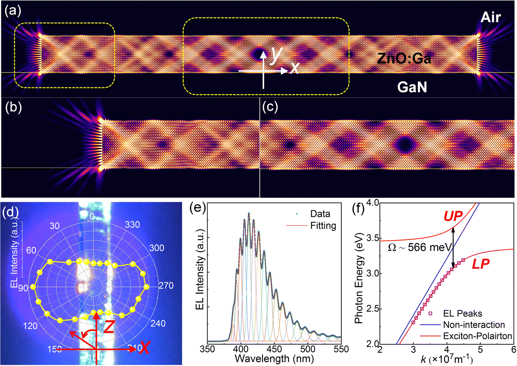 | ||
| Fig. 4 Microcavity effect on the EL characteristics of the n-ZnO:Ga microribbon/p-GaN heterojunction LED. (a) Numerical calculation of standing wave field distribution, which is confinedto the cross-section of the LED structure. Enlarged simulation of (b) region-I, (c) region-II marked in (a). (d) Polar plot of the EL intensity of the LED, which was distributed in the x–z plane. The background image is an optical microscopy EL image. (e) Lorentzian-fitted EL spectrum of the heterojunction device with multiple interference peaks. (f) Energy-wave vector dispersion curve corresponding to the EL spectrum. The exciton–photon coupling strength, called Rabi splitting energy Ω, is extracted approximately 566 meV. | ||
The detection polarization angle 0° is set parallel to the z direction along the length direction of the CVD-synthesized ZnO:Ga microribbon, and the variation in the detection polarization angle with the EL intensity on the x–z plane is explored. The results are plotted in polar coordinates in Fig. 4(d), with the maximum value at approximately 90°. The minimum value is at approximately 0°, which is larger than the expected value of the ideal mode with linear polarization. This phenomenon is related to diffraction at the narrower sides of the microribbon. The angle corresponds to the optical microscopic EL image in the background image. This shows that the luminescence direction of the microribbon on the x–z plane is mainly located in the 90°–270° direction (x-axis direction), i.e., the output directions from the narrower sides of the microribbon, and the device has good linear polarization. The polarization of luminescence is influenced by the modes coupled to the optical microcavity. The electric field polarization dominates in the x direction, while the components in the y and z directions are very weak, which agrees well with the observation results. More interestingly, the EL spectrum with multipeak emission characteristics shown in Fig. 4(e) can be fitted well by the multi-Lorentzian function to determine each resonance peak. From the Lorentzian fitted spectrum, the mode spacing of the resonance peak in the low-energy regime is larger than that in the high-energy regime. The classical photonic crystal model is not sufficient to explain the luminescence of the device. Therefore, the obvious multipeak emission feature of the spectrum can be due to the EP behavior.57
The classical Lorentz oscillator model was used to explore the exciton–photon coupling in the microribbon-based microcavity, in which the refractive index and polaron dispersion can be interpreted by the dielectric approximation form:58
 | (1) |
 | (2) |
The cross-sectional width of the microribbons can wholly confine the light waves, forming optical resonances. The influence of different microribbon widths on the EL characteristics of devices was investigated. Devices were prepared by using ZnO:Ga-microribbons with the same length but different widths of 26, 38, and 45 μm, which correspond to LED-A, LED-B, and LED-C, respectively. Fig. 5(a)–(c) illustrate the EL spectra of the devices with similar injection current ranges. Significantly, a series of narrow peaks can be clearly distinguished on all EL spectra, which are due to the effect of the optical waveguide microcavity constructed by the quadrilateral cross section, so that all EL spectra can show multipeak emission characteristics. With increasing cross-sectional width of the microribbons, the spectral profiles exhibit significant broadening. In addition, the main peak shows a red shift of 399.0–422.3 nm, which is due to the self-absorption of guided light in the microribbon cavity induced by the band tail state.64 Thus, increasing the width of the microribbon can lead to enhanced polariton relaxation, whereby the photons escape from the confinement of the microcavity and release additional energy. In addition, the inhomogeneity of the spectrum spacing toward the longer-wavelength shoulder indicates that the output signals are attenuated in the light-emission region.53,65
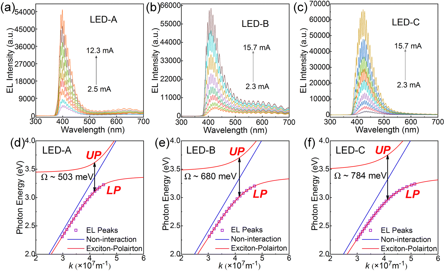 | ||
| Fig. 5 Microribbon width-dependent EL characteristics of the LEDs. (a) EL spectra of LED-A based on a 26 μm width microribbon. (b) EL spectra of LED-B based on a 38 μm width microribbon. (c) EL spectra of LED-C based on a 45 μm width microribbon. (d) LED-A: energy-wave vector dispersion curve (Ω ∼ 503 meV). (e) LED-B: energy-wave vector dispersion curve (Ω ∼ 680 meV). (f) LED-C: energy-wave vector dispersion curve (Ω ∼ 784 meV). | ||
We also gave the energy-wave vector dispersion relationship corresponding to the above devices to explore the influence of the microribbon width on the EP effect in devices. The energy-wave vector dispersion curves of the above three LEDs according to eqn (2) and the corresponding experimental points are shown in Fig. 5(d)–(f), respectively. The large Ω values from the microribbons with different widths are extracted in the figures (about 503, 680, and 784 meV, respectively), and the Ω value increases with the microribbon width. This phenomenon was explained by the increased overlap integral between the exciton and the photon field. That is, the EP coupling strength of the devices can be tunable.61 All the energy-wave vector dispersion curves clearly show anticrossing behavior between the UP and LP branches. At the same time, the photon energy of the EL peak fits the EP model well and is all located in the LP branch.66 Therefore, the prepared devices can simultaneously indicate strong coupling because of their excellent electronic transport properties and high-quality optical resonator, promoting the single-microribbon heterojunction to a favorable platform for low-dimensional lasers.67
Further optimization treatment was carried out. First, the CVD-synthesized ZnO:Ga microribbons, which could satisfy both optical and electrical requirements for the lasing emissions, was achieved through optimizing the growth conditions. The ZnO:Ga microribbon can support the F–P mode lasing upon optical excitation, while the Ga-dopant presented in the ZnO:Ga structure can boost its electronic transport properties, which are conducive to the current injection for the heterojunction devices. Second, heat dissipation, metal–semiconductor contact for current injection, and the device design optimization, were further taken into account, which allows higher injection current operation and possible achievement of a room temperature electrically pumped lasing emissions with a much lower threshold. The I–V characteristic curve is plotted in Fig. 6(a), which shows that the reverse leakage current is much lower. Fig. 6(b) shows the EL spectra under different injection currents, revealing the broad spontaneous emission spectrum observed at low injection currents (0.2–4.7 mA).
 | ||
| Fig. 6 Lasing characterization of optimized n-ZnO:Ga microribbon/p-GaN heterojunction LED. (a) I–V characteristic curve of the device. (b) EL spectra of the device with currents driving from 0.2 to 4.7 mA. (c) EL spectra as the driving current increased beyond 15.0 mA. (d) The changes of integrated EL intensity and spectral FWHM versus the injection current. (e) Magnified EL spectrum plotted at a light-emitting peak of 426.1 nm (∼38.0 mA). The spectrum FWHM of the lasing peak is extracted to about 0.23 nm, and the laser Q-factor is calculated to about 1800. | ||
For the continuous wave (CW) electrically-driven by the driving current in the range of 15.0–38.0 mA, the EL spectra are depicted in Fig. 6(c). From the graph, once the current increased to 28.0 mA, three sharp and separated emission peaks were observed in the EL spectrum, and they were centered at 421.9, 426.1, and 435.0 nm, respectively. The intensity increases rapidly with a further increase in the injection current, indicating the lasing action of the device. The EL spectrum is dominated by three sharp and discrete peaks, and the peak position is almost unchanged. These results demonstrate that the microribbons can work as optical waveguide to achieve high-quality stable lasing outputs. Fig. 6(d) shows the variations in the integrated EL intensity and the FWHM of the device as functions of the injection current. As the injection current increases, there is a significant transition from spontaneous emission to lasing radiation. Soon after the changeover to superlinear behavior, the FWHM decreased sharply from approximately 30 nm to 0.23 nm. From the superlinear behavior, the threshold current of the lasing is estimated approximately to be 25.6 mA. An obvious narrowing of the linewidth and a rapid increase in the nonlinear dependence of the luminescence intensity were observed, which provide strong proof of the lasing behavior.41,49 A magnified EL spectrum in 426.1 nm lasing mode at an injection current of 38.0 mA is shown in Fig. 6(e). The FWHM (δλ) of the lasing peak is extracted to be approximately 0.23 nm, and the estimated quality factor Q calculated using the relationship Q = λ/δλ is approximately 1800. As a result, the quality factor of lasing in the device is significantly higher than that of spontaneous emission in the device. It was confirmed that the observed sharp peak was the lasing in the microribbon.17,41 The results show that CVD-fabricated microribbons are high quality, and allow to achieve high-quality lasing emission at room temperature.
A comparison between the observed lasing peaks and exciton–photon features, achieved under the driving current at a lower level, was evaluated. Fig. 7(a) compares the normalized intensities of ordinary EL (∼4.7 mA lower than the threshold current) and lasing emission (∼38.0 mA above the threshold current). Only a broad spontaneous emission peak centered at around 402 nm can be observed at injection currents lower than the threshold. When the injected current exceeds the threshold, three sharp lasing peaks appear on the shoulder of the spontaneous emission spectrum, and the FWHM of these sharp peaks is approximately 0.2 nm. The sharp lasing peak that appears at injection currents above the threshold indicates the multi-lasing mode behavior of the system. The lasing spectrum profile (red line) shown in Fig. 7(a) suggests that the mode spacing in the low-energy regime is larger than that in the high-energy regime. The observed mode spacing broadening in the low-energy regime phenomenon is obviously different from the classical photon lasing mode, indicating that the general photonic model is inadequate to explain the F–P mode in the device. As the EL characteristics achieved at a low injection current level have been assigned to the EP, the lasing actions achieved at high driving current levels could be attributed to the strong coupling between excitons and F–P microcavity photons in the microribbon. This is strong proof of an EP laser, instead of classical photon lasers.25,37,63
 | ||
| Fig. 7 Polarization properties of EL emissions for the n-ZnO:Ga microribbon/p-GaN heterojunction microlaser device. (a) Normalized EL spectra plotted at injection currents of 4.7 mA (black line) and 38.0 mA (red line) are given for comparison. (b) Energy-wave vector dispersion curve at the injection current of 4.7 mA (Ω ∼ 486 meV). (c) Energy-wave vector dispersion curve at an injection current of 38.0 mA (Ω ∼ 871 meV). | ||
For a given microribbon, the observed values of mode spacing between the neighbouring lasing peaks exhibit a considerable increase as the mode number decreases. The unique changes may be caused by the formation of polaritons in the anticrossing negative curvature LP branch.64 According to eqn (2), the energy-wave vector dispersion curves of the device under ordinary EL and lasing emission are constructed. The energy-wave vector dispersion curve of the microribbon LED is plotted based on the EL image with an injection current of 4.7 mA and the experimental points are shown in Fig. 7(b). The energy-wave vector dispersion curve plotted on account of the lasing spectrum at an injection current of 38.0 mA and the experimental points are shown in Fig. 7(c). The Ω (∼871 meV) in lasing emission exceeds the dissipative energy of both photons and excitons, thus meeting the requirement for the strong coupling condition. The Ω under lasing emission is considerably higher than that under ordinary EL emission (∼486 meV), indicating that the EP coupling strength during lasing emission is considerably higher than that during ordinary EL emission. The effective mass of the quasiparticle is defined by meff = ħ2(d2E/dk2), which can be inferred from Fig. 7(c).68 The calculated LP mass is significantly larger than the bare-photon mass. These results further clearly confirm the formation of an EP laser. Unlike in conventional photonic lasers, population inversion is no longer a prerequisite, which is attributed to the mechanism of boson final-state stimulation, which makes the EP laser have a significantly low threshold.25,69
4 Conclusions
To summarize, we have designed and prepared an electrically driven EP luminescence and lasing device comprising a p-GaN substrate and a single ZnO:Ga-microribbon. In the device, the microribbon has a natural smooth side, which can provide a platform for strong coupling between excitons and cavity photons. The Rabi splitting energy can be tuned in the range of 503–784 meV by varying the cross-sectional sizes of the ZnO:Ga-microribbon, so that the EP coupling strength can be tunable. The giant Rabi splitting energies are helpful for the construction of low-threshold or even threshold-free lasing devices. Based on this, an electrically driven EP laser with a distinct multiple-mode structure is realized at room temperature. The laser device has a much lower threshold of 25.6 mA, effective suppression of spontaneous emission noise, and a high-quality factor of 1800. More importantly, this is due to the EPs formed in the microribbon of the device under current injection. This work clarifies the role of ZnO:Ga-microribbons in the construction of EP lasers and provides insights into the realization of high-quality electrically driven low-dimensional coherent light sources. We also believe that the demonstrated device can be used for the construction of ultralow-threshold lasers in the future.Author contributions
Yuzhou Sun: conceptualization, methodology, and writing – original draft. Mingming Jiang: project administration, funding acquisition, and writing – review & editing. Maosheng Liu: investigation and methodology. Binghui Li: formal analysis, validation, investigation, and resources. Kai Tang: data curation and validation. Peng Wan: visualization, validation, and formal analysis. Chongxin Shan: supervision, project administration, and funding acquisition. Dezhen Shen: supervision and resources.Conflicts of interest
There are no conflicts to declare.Acknowledgements
This study was supported by the National Natural Science Foundation of China (No. 12374257). The authors acknowledge the facilities in the Center for Microscopy and Analysis at Nanjing University of Aeronautics and Astronautics.Notes and references
- Y. Zhang, X. Wang, K. Yan, H. Zhu, B. Wang and B. Zou, Adv. Funct. Mater., 2023, 33, 2211272 CrossRef CAS.
- H. Deng, G. L. Lippi, J. Mørk, J. Wiersig and S. Reitzenstein, Adv. Opt. Mater., 2021, 9, 2100415 CrossRef CAS.
- K. Yoshida, J. Gong, A. L. Kanibolotsky, P. J. Skabara, G. A. Turnbull and I. D. W. Samuel, Nature, 2023, 621, 746 CrossRef CAS PubMed.
- J. Xu, T. Zhang, Y. Li, J. Zhang, Z. Wang, Q. Kan, R. Zhang and C.-Z. Ning, Laser Photonics Rev., 2023, 17, 2200322 CrossRef CAS.
- E. Seker, B. Olyaeefar, K. Dadashi, S. Åžengül, M. H. Teimourpour, R. El-Ganainy and A. Demir, Light: Sci. Appl., 2023, 12, 149 CrossRef CAS PubMed.
- N. Liang, J. Yan and T. Zhai, Laser Photon. Rev., 2023, 17, 2300343 CrossRef.
- Q. Chen, Z. Qi, J. Lin, J. Huang and G. Xie, Innovation, 2023, 4, 100498 Search PubMed.
- Q. Bao, W. Li, P. Xu, M. Zhang, D. Dai, P. Wang, X. Guo and L. Tong, Light: Sci. Appl., 2020, 9, 42 CrossRef CAS PubMed.
- E. Dimopoulos, M. Xiong, A. Sakanas, A. Marchevsky, G. Dong, Y. Yu, E. Semenova, J. Mørk and K. Yvind, Optica, 2023, 10, 973–976 CrossRef.
- R. Yi, X. Zhang, C. Li, B. Zhao, J. Wang, Z. Li, X. Gan, L. Li, Z. Li, F. Zhang, L. Fang, N. Wang, P. Chen, W. Lu, L. Fu, J. Zhao, H. H. Tan and C. Jagadish, Light: Sci. Appl., 2022, 11, 120 CrossRef CAS PubMed.
- H. Li, Z. Wang, L. Wang, Y. Tan and F. Chen, Light: Sci. Appl., 2023, 12, 223 CrossRef CAS PubMed.
- S. Cheng, Z. Qiao, Z. Wang, L. Xiao, S. Das, Y. T. Thung, Z. Yuan, V. D. Ta, W. Fan, Y.-C. Chen and H. Sun, Adv. Opt. Mater., 2023, 11, 2203133 CrossRef CAS.
- S. Jiang, C. Xia, R. Ji, H. Pang, D. Li, D. Yang and X. Ma, ACS Appl. Mater. Interfaces, 2024, 16, 3719–3725 CrossRef CAS PubMed.
- X. Yang, C.-X. Shan, P.-N. Ni, M.-M. Jiang, A.-Q. Chen, H. Zhu, J.-H. Zang, Y.-J. Lu and D.-Z. Shen, Nanoscale, 2018, 10, 9602–9607 RSC.
- Z. Wang, Y. Ren, Y. Wang, Z. Gu, X. Li and H. Sun, Appl. Phys. Lett., 2019, 115, 111103 CrossRef.
- A. Liu, G. Guan, X. Chai, N. Feng, M. Lu, X. Bai and Y. Zhang, Laser Photonics Rev., 2022, 16, 2200189 CrossRef CAS.
- B. Nikoobakht, R. P. Hansen, Y. Zong, A. Agrawal, M. Shur and J. Tersoff, Sci. Adv., 2020, 6, eaba4346 CrossRef CAS PubMed.
- A. Consoli, N. Caselli and C. Lopez, Nat. Photonics, 2022, 16, 219 CrossRef CAS.
- X. Li, S. Liu, Y. Wei, J. Ma, C. Song, Y. Yu, R. Su, W. Geng, H. Ni, H. Liu, X. Su, Z. Niu, Y.-L. Chen and J. Liu, Light: Sci. Appl., 2023, 12, 65 CrossRef CAS PubMed.
- X. Zhou, M. Jiang, K. Xu, M. Liu, S. Sha, S. Cao, C. Kan and D. N. Shi, Light: Sci. Appl., 2022, 11, 198 CrossRef CAS PubMed.
- K. Ren, C. Li, Z. Fang and F. Feng, Laser Photon. Rev., 2023, 17, 2200758 CrossRef.
- Z. Li, W. Liu, R. Wang, F. Chen, J. Chen, Y. Zhu, Z. Shi and C. Xu, Nano Energy, 2022, 93, 106832 CrossRef CAS.
- K. Tang, P. Wan, C. Kan, M. Liu, D. Shi and M. Jiang, Appl. Phys. Lett., 2022, 120, 011105 CrossRef CAS.
- X. Zhou, M. Jiang, J. Wu, M. Liu, C. Kan and D. Shi, Opt. Express, 2022, 30, 18273–18286 CrossRef CAS PubMed.
- M. D. Fraser, S. Hoefling and Y. Yamamoto, Nat. Mater., 2016, 15, 1049–1052 CrossRef CAS PubMed.
- W. Mao, M. Jiang, J. Ji, P. Wan, X. Zhou and C. Kan, Photon. Res., 2020, 8, 175–185 CrossRef CAS.
- G. Kreyder, L. Hermet, P. Disseix, F. Médard, M. Mihailovic, F. Réveret, S. Bouchoule, C. Deparis, J. Zuñiga-Pérez and J. Leymarie, Phys. Rev. B, 2023, 107, 125307 CrossRef CAS.
- C.-Y. Huang, C. Zou, C. Mao, K. L. Corp, Y.-C. Yao, Y.-J. Lee, C. W. Schlenker, A. K. Y. Jen and L. Y. Lin, ACS Photonics, 2017, 4, 2281–2289 CrossRef CAS.
- M. Leng, J. Wu, K. Dini, J. Liu, Z. Hu, J. Tang, T. C. H. Liew, H. Sun, R. Su and Q. Xiong, ACS Photonics, 2023, 10, 1349–1355 CrossRef CAS.
- Q. Zhang, S.-W. Wang, X. Liu, T. Chen, H. Li, J. Liang, W. Zheng, R. Agarwal, W. Lu and A. Pan, Nano Energy, 2016, 30, 481–487 CrossRef CAS.
- F. Chen, H. Li, H. Zhou, S. Luo, Z. Sun, Z. Ye, F. Sun, J. Wang, Y. Zheng, X. Chen, H. Xu, H. Xu, T. Byrnes, Z. Chen and J. Wu, Phys. Rev. Lett., 2022, 129, 057402 CrossRef CAS PubMed.
- T. Matsuo, Y. Ueda, H. Mizuno, F. Sasaki, K. Yamashita and H. Yanagi, ACS Photonics, 2022, 9, 2015–2023 CrossRef CAS.
- Z. Ye, F. Chen, H. Zhou, S. Luo, Z. Sun, H. Xu, H. Xu, H. Li, Z. Chen and J. Wu, Phys. Rev. B, 2023, 107, L060303 CrossRef CAS.
- Y. Wang, P. G. Lagoudakis and H. Sigurdsson, Phys. Rev. B, 2022, 106, 245304 CrossRef CAS.
- F. Chen, H. Zhou, Z. Ye, S. Luo, Z. Sun, Y. Zheng, X. Chen, H. Xu, H. Xu, T. Byrnes, H. Li, Z. Chen and J. Wu, Phys. Rev. B, 2022, 106, L020301 CrossRef CAS.
- S.-U. Kim, D.-Y. Um, J.-K. Oh, B. Chandran, C.-R. Lee and Y.-H. Ra, ACS Photonics, 2023, 10, 1053–1059 CrossRef CAS.
- T. Wang, Z. Zang, Y. Gao, C. Lyu, P. Gu, Y. Yao, K. Peng, K. Watanabe, T. Taniguchi, X. Liu, Y. Gao, W. Bao and Y. Ye, Nano Lett., 2022, 22, 5175–5181 CrossRef CAS PubMed.
- Q. Shang, M. Li, L. Zhao, D. Chen, S. Zhang, S. Chen, P. Gao, C. Shen, J. Xing, G. Xing, B. Shen, X. Liu and Q. Zhang, Nano Lett., 2020, 20, 6636–6643 CrossRef CAS PubMed.
- R. Su, A. Fieramosca, Q. Zhang, H. S. Nguyen, E. Deleporte, Z. Chen, D. Sanvitto, T. C. H. Liew and Q. Xiong, Nat. Mater., 2021, 20, 1315–1324 CrossRef CAS PubMed.
- S. Sha, K. Tang, M. Liu, P. Wan, C. Zhu, D. Shi, C. Kan and M. Jiang, Photon. Res., 2024, 12, 648–662 CrossRef.
- Z. Li, M. Jiang, Y. Sun, Z. Zhang, B. Li, H. Zhao, C. Shan and D. Shen, Nanoscale, 2018, 10, 18774–18785 RSC.
- Y. Sun, M. Jiang, B. Li, X. Xie, C. Shan and D. Shen, Opt. Express, 2022, 30, 740–753 CrossRef CAS PubMed.
- Z. Li, G. He, M. Jiang, J. Ji, C. Shan and D. Shen, J. Mater. Chem. C, 2019, 7, 10933–10944 RSC.
- M. Jiang, W. Mao, X. Zhou, C. Kan and D. Shi, ACS Appl. Mater. Interfaces, 2019, 11, 11800–11811 CrossRef CAS PubMed.
- L. Sun, J. Li, J. Han, M. Liu, M. Meng, B. Li and M. Jiang, Results Phys., 2023, 54, 107065 CrossRef.
- J. Dai, C. Xu, T. Nakamura, Y. Wang, J. Li and Y. Lin, Opt. Express, 2014, 22, 28831–28837 CrossRef PubMed.
- G. Weng, J. Tian, S. Chen, J. Yan, H. Zhang, Y. Liu, C. Zhao, X. Hu, X. Luo, J. Tao, S. Chen, Z. Zhu, J. Chu and H. Akiyama, ACS Photonics, 2021, 8, 787–797 CrossRef CAS.
- M. Jiang, G. He, H. Chen, Z. Zhang, L. Zheng, C. Shan, D. Shen and X. Fang, Small, 2017, 13, 1604034 CrossRef PubMed.
- J. Dai, C. X. Xu and X. W. Sun, Adv. Mater., 2011, 23, 4115–4119 CrossRef CAS PubMed.
- M. Liu, Z. Yang, S. Sha, K. Tang, P. Wan, C. Kan, D. N. Shi and M. Jiang, ACS Appl. Mater. Interfaces, 2023, 15, 54655–54666 CrossRef CAS PubMed.
- T. A. Growden, W. Zhang, E. R. Brown, D. F. Storm, D. J. Meyer and P. R. Berger, Light: Sci. Appl., 2018, 7, 17150 CrossRef CAS PubMed.
- B. Zhao, F. Wang, H. Chen, L. Zheng, L. Su, D. Zhao and X. Fang, Adv. Funct. Mater., 2017, 27, 1700264 CrossRef.
- M. Liu, M. Jiang, Q. Zhao, K. Tang, S. Sha, B. Li, C. Kan and D. N. Shi, ACS Appl. Mater. Interfaces, 2023, 15, 13258–13269 CrossRef CAS PubMed.
- W. Song, X. Wang, H. Chen, D. Guo, M. Qi, H. Wang, X. Luo, X. Luo, G. Li and S. Li, J. Mater. Chem. C, 2017, 5, 11551–11558 RSC.
- T. Liu, P. Ran, Y. Su, Z. Chen, R. Lai, W. Shen, Y. Ma, H. Zhu and Y. M. Yang, Photon. Res., 2023, 11, 1791–1801 CrossRef.
- C. Xu, F. Qin, Q. Zhu, J. Lu, Y. Wang, J. Li, Y. Lin, Q. Cui, Z. Shi and A. G. Manohari, Nano Res., 2018, 11, 3050–3064 CrossRef CAS.
- Y.-H. Ra, R. T. Rashid, X. Liu, S. M. Sadaf, K. Mashooq and Z. Mi, Sci. Adv., 2020, 6, eaav7523 CrossRef CAS PubMed.
- J. Lagois, Phys. Rev. B: Condens. Matter Mater. Phys., 1981, 23, 5511–5520 CrossRef CAS.
- L. K. van Vugt, S. Rühle, P. Ravindran, H. C. Gerritsen, L. Kuipers and D. Vanmaekelbergh, Phys. Rev. Lett., 2006, 97, 147401 CrossRef PubMed.
- M. A. Kaliteevski, S. Brand, R. A. Abram, A. Kavokin and L. S. Dang, Phys. Rev. B: Condens. Matter Mater. Phys., 2007, 75, 233309 CrossRef.
- Q. Shang, C. Li, S. Zhang, Y. Liang, Z. Liu, X. Liu and Q. Zhang, Nano Lett., 2020, 20, 1023–1032 CrossRef CAS PubMed.
- W. Du, S. Zhang, J. Shi, J. Chen, Z. Wu, Y. Mi, Z. Liu, Y. Li, X. Sui, R. Wang, X. Qiu, T. Wu, Y. Xiao, Q. Zhang and X. Liu, ACS Photonics, 2018, 5, 2051–2059 CrossRef CAS.
- K. Park, J. W. Lee, J. D. Kim, N. S. Han, D. M. Jang, S. Jeong, J. Park and J. K. Song, J. Phys. Chem. Lett., 2016, 7, 3703–3710 CrossRef CAS PubMed.
- X. Wang, M. Shoaib, X. Wang, X. Zhang, M. He, Z. Luo, W. Zheng, H. Li, T. Yang, X. Zhu, L. Ma and A. Pan, ACS Nano, 2018, 12, 6170–6178 CrossRef CAS PubMed.
- S. Zhang, Q. Shang, W. Du, J. Shi, Z. Wu, Y. Mi, J. Chen, F. Liu, Y. Li, M. Liu, Q. Zhang and X. Liu, Adv. Opt. Mater., 2018, 6, 1701032 CrossRef.
- M. Held, A. Graf, Y. Zakharko, P. Chao, L. Tropf, M. C. Gather and J. Zaumseil, Adv. Opt. Mater., 2018, 6, 1700962 CrossRef.
- R. Jayaprakash, K. Georgiou, H. Coulthard, A. Askitopoulos, S. K. Rajendran, D. M. Coles, A. J. Musser, J. Clark, I. D. W. Samuel, G. A. Turnbull, P. G. Lagoudakis and D. G. Lidzey, Light: Sci. Appl., 2019, 8, 81 CrossRef PubMed.
- H. Deng, G. Weihs, C. Santori, J. Bloch and Y. Yamamoto, Science, 2002, 298, 199–202 CrossRef CAS PubMed.
- F. Riminucci, V. Ardizzone, L. Francaviglia, M. Lorenzon, C. Stavrakas, S. Dhuey, A. Schwartzberg, S. Zanotti, D. Gerace, K. Baldwin, L. N. Pfeiffer, G. Gigli, D. F. Ogletree, A. Weber-Bargioni, S. Cabrini and D. Sanvitto, Phys. Rev. Appl., 2022, 18, 024039 CrossRef CAS.
| This journal is © The Royal Society of Chemistry 2024 |