
 Open Access Article
 This Open Access Article is licensed under a Creative Commons Attribution-Non Commercial 3.0 Unported Licence
Improved electrical performance of ultra-thin BexMg1−xO films using super-cycle atomic layer deposition†
Haewon
Song
,
Bowen
Wang
,
Jonghoon
Shin
,
Yu-Kyung
Park
,
Tae Kyun
Kim
,
Heewon
Paik
,
Haengha
Seo
,
Junil
Lim
,
Daeson
Kwon
,
Keonuk
Lee
,
Young Sin
Kim
,
Dong Hoon
Shin
and
Cheol Seong
Hwang
 *
*
Department of Materials Science and Engineering, and Inter-University Semiconductor Research Center, Seoul National University, Seoul, 08826, Republic of Korea. E-mail: cheolsh@snu.ac.kr
First published on 23rd January 2024
Abstract
This research explores the high-k dielectric behavior of ultra-thin BeMgO (BMO) films (≪5 nm) using the super-cycle atomic layer deposition (ALD) technique. The fabricated metal–insulator–metal devices, utilizing sputtered TiN as both bottom and top electrodes, demonstrate low leakage current and high capacitance characteristics with a minimum equivalent oxide thickness of 1.30 nm. The dielectric constants of the films are significantly higher than those of pure MgO or BeO films, reaching a maximum value of 14.2 at a film composition of Be0.29Mg0.71O, indicating the realization of the cubic rocksalt configuration of Be–O bonds. The rocksalt phase remains dominant even in Be-rich BMO films due to the structural coherence with the TiN electrodes, revealing the intricate interplay between composition and interface engineering. BMO films showed exceptional electrical stability even at a film thickness of 2.5 nm, demonstrating their strong dielectric strength. The trap-assisted tunneling mechanism governed the leakage current at this thickness. Such attributes make BMO films highly appealing in dynamic random-access memory capacitors, where the industry's relentless drive toward miniaturization necessitates ultra-thin dielectric films with uncompromising performance.
Introduction
The trade-off relationship between dielectric constant and bandgap has long been recognized as challenging in searching for new high-k (k = dielectric constant) dielectric materials for semiconductor applications, particularly in developing DRAM capacitors.1 Ongoing research is focused on optimizing dielectric materials to achieve sufficiently low leakage current while maintaining high capacitance.2–4 Extensive studies have been conducted on group IV binary oxides such as HfO2,5,6 ZrO27–10 and TiO2,11–13 as well as perovskite dielectrics like SrTiO3,14–16 exploring various modifications through doping or lamination with different dielectric materials. However, these modifications have yet to enhance the dielectric constant itself substantially.The k and the bandgap (Eg) of wurtzite (WZ) phase beryllium oxide (BeO) are 6.917 and 10.6 eV,18 respectively, representing the trade-off relation. Nonetheless, BeO has been spotlighted for its high thermal conductivity,19 high thermal endurance,20–23 mechanical strength,24–28 and chemical stability.29,30 The thermal conductivity value of BeO of 300 W K−1 m−1 is the second-highest value among all the known materials after diamond. Besides, a recent theoretical study reported that the rocksalt (RS) BeO can exhibit a dielectric constant of 275 and a bandgap of 10.1 eV.31 This finding suggested a method to break the trade-off relationship and triggered several follow-up research studies. However, the RS BeO has not yet been realized with existing deposition techniques because RS BeO is stable only over an extremely high hydrostatic pressure of 130 GPa.22,32–35 The theoretical study has assumed such a high pressure to ensure the RS BeO structure and released the pressure to atmospheric value.31 In this case, the RS structure could be retained theoretically, but the experimental process can hardly follow such a process, rendering stabilizing the RS BeO at atmospheric pressure impractical.
Therefore, a different approach has been attempted. MgO is a well-known dielectric material with the RS structure with k and Eg values of 9.4 and 7.4 eV, respectively,36 which may serve as the framework of the RS BeO when mixed or the template layer when deposited alternatively. It was expected that the Be- and Mg-rich BeMgO (BMO) films would have WZ and RS structures, respectively, which has been experimentally proven.37
Therefore, BMO films were deposited by the super-cycle atomic layer deposition (ALD) method, which can ensure conformal deposition over the three-dimensional structure of the highly scaled semiconductor device. Super-cycle ALD is also useful to control the Be![[thin space (1/6-em)]](https://www.rsc.org/images/entities/char_2009.gif) :Mg ratio of the film by changing the BeO and MgO ALD cycle ratio. The authors’ group has reported a feasible super-cycle ALD approach to growing BMO films using dimethylberyllium (DMBe) and bis(ethylcyclopentadienyl)magnesium (Mg(EtCp)2) as a precursor for Be and Mg sources with H2O as an oxygen source.37 Be0.21Mg0.79O films exhibited a k value of ∼18 while maintaining a large bandgap of >8 eV, owing to the stabilization of Be–O configuration as RS. However, Be-richer BMO films showed a WZ structure with lower k-values. These results were consistent with the computational simulations that the modified RS phase is stable up to x ∼ 0.3 and exhibits a k value of ∼18.38 Still, it was not assured that these outcomes were ultimately achievable performances given that the MgO was susceptible to degradation by its natural hygroscopic properties when exposed to H2O during the H2O-based ALD process.39
:Mg ratio of the film by changing the BeO and MgO ALD cycle ratio. The authors’ group has reported a feasible super-cycle ALD approach to growing BMO films using dimethylberyllium (DMBe) and bis(ethylcyclopentadienyl)magnesium (Mg(EtCp)2) as a precursor for Be and Mg sources with H2O as an oxygen source.37 Be0.21Mg0.79O films exhibited a k value of ∼18 while maintaining a large bandgap of >8 eV, owing to the stabilization of Be–O configuration as RS. However, Be-richer BMO films showed a WZ structure with lower k-values. These results were consistent with the computational simulations that the modified RS phase is stable up to x ∼ 0.3 and exhibits a k value of ∼18.38 Still, it was not assured that these outcomes were ultimately achievable performances given that the MgO was susceptible to degradation by its natural hygroscopic properties when exposed to H2O during the H2O-based ALD process.39
In the following research for the MgO ALD, it was discovered that ozone (O3) as an oxygen source eliminated such a problem.40 Also, in situ crystallization of MgO film was achievable when the MgO film was grown on a TiN bottom electrode, owing to crystal structure coherency between TiN and MgO. With these improvements, the leakage current of MgO film could be decreased by more than three orders of magnitude.40
Therefore, this study utilizes super-cycle ALD with O3 to deposit ultra-thin BMO films, aiming to overcome the constraints of previous H2O-based ALD. The electrical performances of BMO films with varying Be contents were evaluated using a MIM capacitor structure, striving to surpass the performance of existing BeO and MgO thin films. The careful structural and chemical analysis further substantiates the enhancements in the electrical performance. Additionally, the potential of these films for dynamic random-access memory (DRAM) capacitor applications was explored, particularly emphasizing the importance of thin film scalability in modern semiconductor technology.
Experimental procedure
Atomic layer deposition
A 4-inch-scale single-wafer showerhead type ALD reactor (CN-1, Atomic Premium) was adopted to deposit the BeO and MgO thin films. ALD was performed using Diethylberyllium (DEBe) and Bis(cyclopentadienyl)magnesium (MgCp2) as Be and Mg precursors, respectively. O3 with a concentration of 180 g Nm−3 was used as the oxygen source. Argon gas (99.9999% purity) was employed as a purge gas at a flow rate of 1000 standard cubic centimeters per min (sccm) and as a carrier gas during the precursor feeding step with a flow rate of 80 sccm. The ALD process consisted of sub-cycles comprising precursor feeding, Ar purging, O3 feeding, and Ar purging steps. The Be–O sub-cycle followed a sequence of 2-30-5-30, with the duration of each step in seconds. Similarly, the Mg–O sub-cycle followed a sequence of 6-30-6-30. The BMO thin film was deposited using a super-cycle ALD approach, as illustrated in Fig. 1(a), where a super-cycle with a specific ratio of the Be–O and Mg–O sub-cycles was repeated.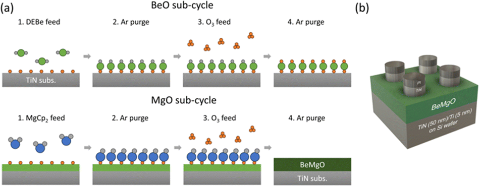 | ||
| Fig. 1 Schematic representation of (a) the super-cycle ALD technique used for BMO film deposition. The BMO composition is controlled by adjusting the BeO and MgO sub-cycle ratios. (b) Illustration of the MIM-structured device, designed to assess the electrical performance of the fabricated films. | ||
Both MgO and BeO exhibited ALD temperature windows of 300–350 °C, but peculiarities related to excessive deposition were observed during BMO deposition within this temperature range. Therefore, a growth temperature of 275 °C, slightly lower than the ALD window of MgO and BeO films, was adopted in this study. Although the MgO and BeO film growth per cycle (GPC) was slightly higher and lower, respectively, than their saturated GPC in the ALD window, no peculiarities were observed in BMO super-cycle deposition at this temperature. Post-deposition annealing (PDA) was performed using a rapid thermal annealing process under an O2 atmosphere for 5 minutes at a temperature of 500 °C, which has been identified as the best condition for achieving stable electrical properties.
Annealing treatment
Post-deposition annealing (PDA) was performed using a rapid thermal annealing (RTA, Korea Vacuum Tech, KVR-3006T) process under an O2 atmosphere for 5 minutes at a temperature of 500 °C, which has been identified as the best condition for achieving stable electrical properties.40Physical and chemical analysis
The thickness of the deposited BMO thin film was measured using spectroscopic ellipsometry (J. A. Woollam, ESM-300), and the measured thickness was validated by cross-section field-emission transmission electron microscopy (FE-TEM, JEM-F200). The crystal structure of the deposited BMO film was analyzed with grazing incidence (ω = 0.5°) X-ray diffraction (GAXRD, PANalytical, X’pert Pro) using Cu Kα X-ray radiation. The composition of the deposited BMO film was analyzed using Auger electron spectroscopy (AES) (PHI-710), and the bonding states of the film were examined using X-ray photoelectron spectroscopy (XPS) (AXIS SUPRA).Electrical analysis
As shown in Fig. 1(b), MIM capacitors were fabricated using a stack comprising 30 nm Pt/10 nm TiN/BMO thin film/50 nm TiN/5 nm Ti/100 nm SiO2/Si. The SiO2 layer was formed by the thermal oxidation of a Si(100) wafer, followed by a 5 nm Ti layer deposition and a 50 nm TiN layer (bottom electrode, BE) using reactive sputtering (Applied Materials, Endura). A shadow mask with a 300 μm diameter hole pattern was employed for the top electrode deposition, and a 10 nm TiN layer and a 30 nm Pt layer (top electrode, TE) were deposited using DC magnetron sputtering (EQCELL, SNTEK).Capacitance–voltage (C–V) and current density–voltage (J–V) measurements were conducted using an HP 4194A impedance analyzer and an HP 4140D picoammeter. All measurements were performed with the bottom electrode layer grounded while bias was applied to the top electrode. During C–V measurements, a voltage sweep ranging from −1.5 V to +1.5 V was applied, while J–V measurements involved voltage sweeps from 0 V to 1.5 V and from 0 V to −1.5 V.
Results and discussion
Fig. 2(a) shows the variation of the BMO film thickness as a function of the super-cycle (s-cy) ALD numbers with different BeO:MgO cycle ratios (cycle ratio). The cycle ratios chosen were 1:2, 1:1, and 2:1, resulting in GPC values of 0.43 nm s-cy−1, 0.22 nm s-cy−1, and 0.32 nm s-cy−1, respectively. These values are consistent with the calculated values based on the formula GPCa:b = a × GPCMgO + b × GPCBeO, using the known GPC values of MgO (0.15 nm cy−1) and BeO (0.09 nm cy−1) in previous studies40,41 (The calculated values were GPC1:2 = 0.39 nm s-cy−1, GPC1:1 = 0.24 nm s-cy−1, and GPC2:1 = 0.33 nm s-cy−1). Fig. 2(b) shows the composition of BMO films deposited with various cycle ratios determined by AES. Fig. S1 of online ESI,† shows the spectra. It was observed that the Be composition ratio in the BMO film increases proportionally with the increases in the BeO cycle ratio. However, the Be composition ratio is slightly lower than the expected value from the ALD cycle ratio, suggesting slight retardation of BeO film nucleation on MgO film.
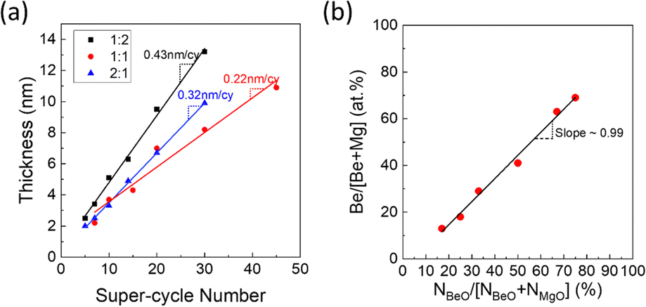 | ||
| Fig. 2 (a) Relationship between the number of super-cycles and film thickness (growth per cycle, GPC) for various sub-cycle ratios. (b) Correlation between sub-cycle ratio and atomic ratio, estimated by AES (see Fig. S1, ESI† for details). | ||
These two results indicate that the surface reactions in the super-cycle ALD process were similar to those in the ALD growth of each binary oxide, even though the growth temperature adopted for BMO deposition (275 °C) was slightly lower than the ALD temperature window for BeO and MgO films. Anomalous growth behavior, such as incomplete ligand exchange reaction or incomplete ligand fraction elimination, reported for BeO42 and MgO ALD40 conducted at temperatures below the ALD window, could be effectively suppressed by alternately progressing sub-cycles of BeO and MgO films. This finding is further proven by the XPS data shown in Fig. 3.
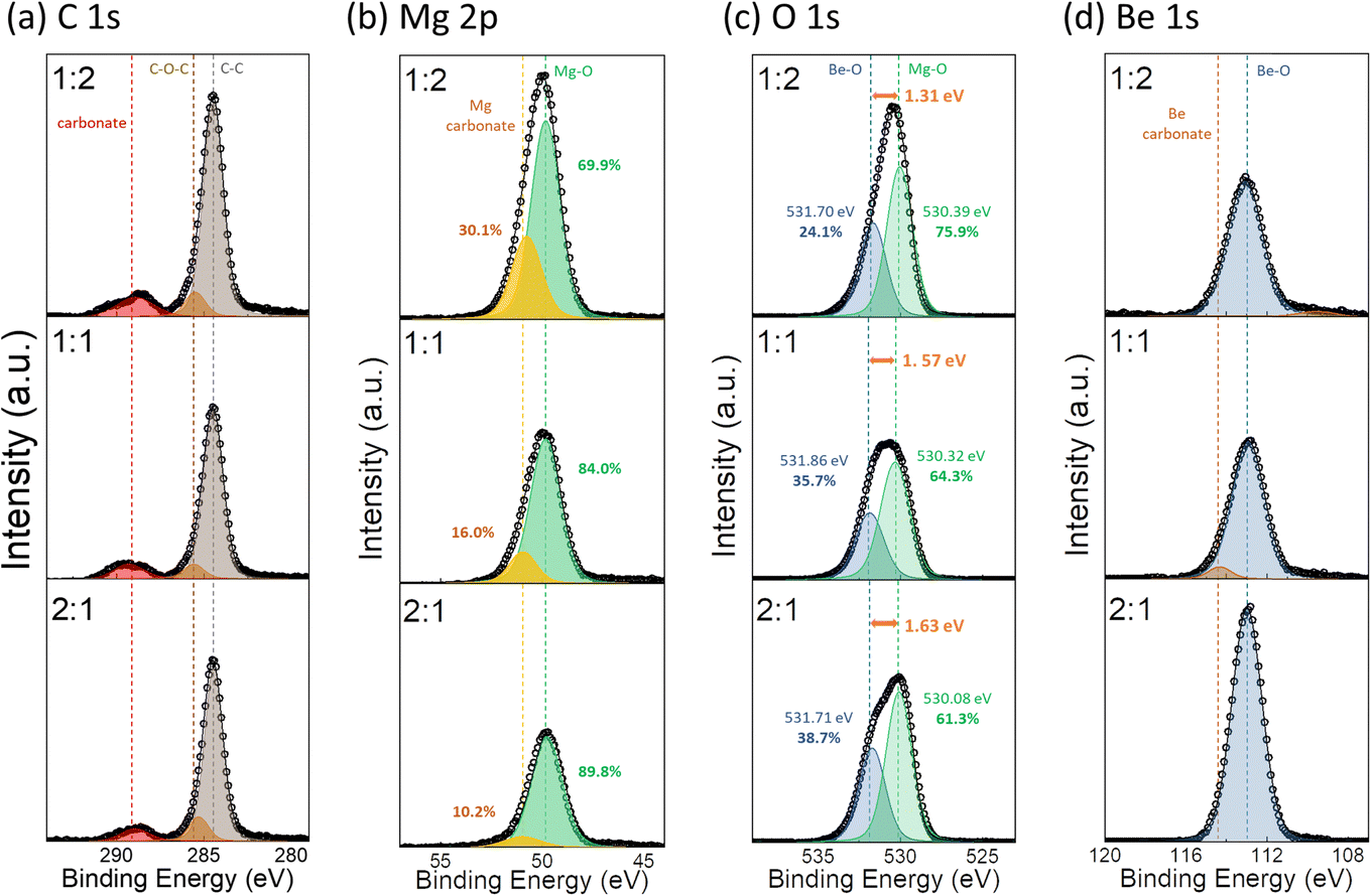 | ||
| Fig. 3 XPS narrow scan spectra of BMO films on TiN substrate, presenting (a) C 1s, (b) Mg 2p, (c) O 1s, and (d) Be 1s peaks. Each peak has been deconvoluted for the best fit, following calibration where the C–C bond peak is fixed at 284.5 eV. | ||
Fig. 3(a)–(d) present the XPS narrow scan results for the elements O, Be, Mg, and impurity C. A binding energy calibration was conducted using the adventitious C–C bond peak at 284.5 eV, as depicted in Fig. 3(a). Examining the Mg 2p peak in Fig. 3(b), it can be observed that the peaks have two components corresponding to Mg–carbonate (50.7 eV) and MgO (49.8 eV).43 Also, the overall peak area decreases as Mg content decreases, and the relative intensity of the Mg–carbonate peak decreases from 30.1% to 10.2% as the BeO cycle ratio increases. A consistent trend is observed in Fig. 3(a), where the carbonate and C–O–C peak intensities diminish with increasing BeO cycle ratio. According to a previous study on MgO ALD involving MgCp2 and O3,40 the Cp ligand of the MgCp2 ruptures during the O3 pulse step, leading to carbon-containing –O–Cx fragments on the surface. At the low deposition temperature of 275 °C, as in this study, ruptured ligands of –O–Cx were not completely removed, leading to increased impurity content within the film. The decrease in the relative intensity of the Mg carbonate peak of Mg 2p spectra and the carbonate peak in C 1s spectra with the increasing Be–O cycle ratio indicates the suppression of such undesired growth behavior observed during MgO single film deposition. This improvement is due to the small molecular size of the Be precursor, DEBe. When the MgO cycle is followed by another MgO cycle, the large size of the MgCp2 precursor hinders it from reaching the –O–Cx bonding site through the Cx-carbonate chain. In contrast, when the BeO cycle follows the MgO cycle, the small-sized DEBe molecules can reach the –O–Cx bonding site and facilitate ligand exchange to –O–Be–OH, thereby removing the Cx chain efficiently and enabling normal ALD with fewer impurities.
The O 1s spectra in Fig. 3(c) were also deconvoluted into two peaks. Considering that the Be–O bond is expected to have a stronger bonding than the Mg–O bond in the BMO solid solution, the peaks with the higher and lower binding energies were interpreted as the Be–O and Mg–O bond, respectively. The positions of the deconvoluted peaks are in reasonable agreement with the literature values of the O 1s peaks in BeO and MgO single films. (BeO: 531.1 eV, MgO: 529.4 eV).40,44 The ratio of the peak areas for the Be–O bond increases in the order of 1:2, 1:1, and 2:1, following the BeO cycle ratio, and the variation in the peak area of the Be 1s peak in Fig. 3(d) shows a similar trend. However, it is noteworthy that the energy difference between the two deconvoluted O 1s peaks increases with the increase in Be content (from 1.31 to 1.63 eV). According to a previous study on BMO films,31,37 the higher dielectric constant observed in BMO films is attributed to the elongation of the Be–O bond length and the softening of the optical phonon mode when the Be–O bond is incorporated into the RS MgO framework. This theory implies that the strength of the Be–O bonds in the RS phase is weaker than that in WZ BeO. Therefore, the higher binding energy difference between the peaks with increasing Be content indicates a gradual transition of the Be–O configuration from RS with lower binding energy to WZ with higher binding energy.45
Fig. 4 presents the phase analysis results conducted using GIXRD to investigate the crystallographic factors contributing to the increase in dielectric constant. Fig. 6(a) shows peaks at ∼36.7° and 42.7°, corresponding to the (111) and (200) planes of RS MgO or RS TiN, respectively. However, it is difficult to precisely determine the origin of these peaks from which layer, as MgO and the TiN have similar lattice constants and share the same crystal structure (MgO: rocksalt, a = 0.421 nm, #45-0946; TiN: rocksalt, a = 0.424 nm, #38-1420). The peak at 41–44°, which corresponds to the (200) peak of RS TiN or MgO, was background subtracted and deconvoluted into peaks of MgO and TiN, as shown in Fig. 4(b). The peak of the TiN substrate was inspected and used as a reference peak for deconvolution. The coexistence of MgO and TiN RS peaks implies that MgO followed the TiN substrate's preferred orientation, suggesting local epitaxial growth, as reported in the previous MgO research.40
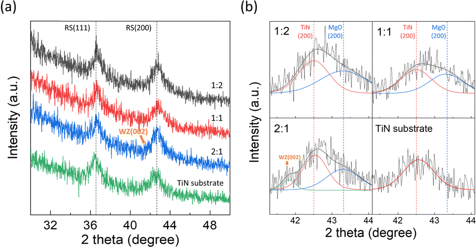 | ||
| Fig. 4 (a) Grazing incidence X-ray diffraction (GIXRD) spectra of BMO samples following post-deposition annealing (PDA) at 500 °C, compared with a bare TiN substrate. (b) An expanded view of the GIXRD spectra in the 2 theta range of 41–44°, featuring background subtraction and peak deconvolution for detailed analysis. | ||
Notable observations were made in the 2:1 sample with the highest Be content. A small peak was observed at ∼41.7° on the left edge of the RS (200) peak. This small peak can be attributed to the WZ (002) peak,46 as confirmed by the magnified and background-subtracted spectra of the peak region in Fig. 4(b) and the Gaussian fitting results of the peak. It can be inferred that in the 2:1 sample, with a composition of Be0.63Mg0.37O, Be atoms do not fully incorporate into the RS MgO framework but instead segregate into a distinct WZ phase.
Cross-section TEM analysis was performed on the same samples after depositing the TiN top electrode to examine the microstructure of the BMO film in more detail. Images were obtained from at least eight different locations within the prepared specimens, and a survey was conducted by analyzing the fast Fourier transform (FFT) signals from multiple regions in each image to investigate the crystal structure. The TEM images of each sample and the FFT patterns of the chosen region are indicated by a red or yellow box in Fig. 5. All samples were found to be polycrystalline, with the 1:1 and 2:1 samples showing some regions that were not fully crystallized. In the 1:2 sample, only the interplanar distance corresponding to the RS MgO phase was observed at all locations, as shown in Fig. 5(a). In contrast, the 1:1 and 2:1 samples manifested an interplanar distance of 0.16 nm, coinciding with the WZ BeO phase, albeit sporadically. These findings corroborate that the 1:2 sample forms a complete solid solution in which BeO is fully dissolved into the RS MgO framework.
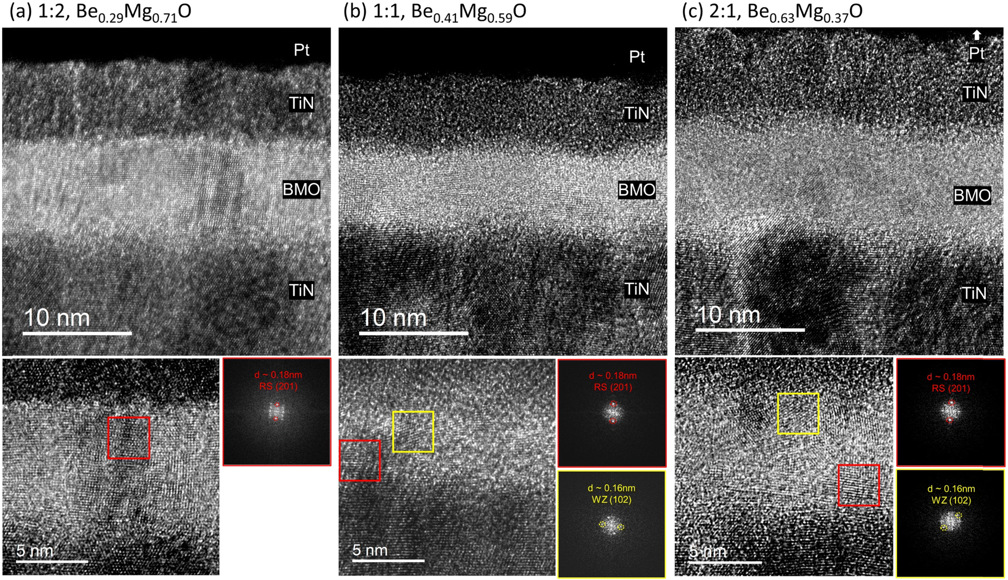 | ||
| Fig. 5 Transmission electron microscopy (TEM) images presenting the cross-sectional view of the top-Pt/TiN/BMO/bottom-TiN stack. High-resolution images of the BMO layer are provided along with fast Fourier transform (FFT) patterns from selected areas of metal–insulator–metal (MIM) devices. These devices utilize BMO films fabricated with a total cycle count of 60, and with different sub-cycle ratios: (a) 1:2, (b) 1:1, and (c) 2:1. | ||
Conversely, a phase separation occurs in the 1:1 and 2:1 samples, culminating in a distinct WZ BeO phase. Although the presence of WZ BeO in the 2:1 sample was previously inferred from the GIXRD results shown in Fig. 4, no such peak was observed for the 1:1 sample. This discrepancy could be attributed to the reduced Be content and a smaller quantity of WZ BeO in the 1:1 sample. Furthermore, even in the 2:1 sample, where Be-content was 63%, WZ BeO was not universally present, suggesting that many Be atoms still contribute to a solid solution with MgO as RS.
The epitaxial coherence between the TiN and MgO layers might account for the continued predominance of the RS phase even in Be-rich samples. A previous study has confirmed the continuous crystallinity from the bottom TiN layer through the MgO layer to the top TiN layer in MIM devices that utilize TiN as the top and bottom electrodes.40 In the TEM images in Fig. 5, the atomic arrangements between the bottom TiN layer and the BMO layers appear consistent, inferring that the TiN substrate effectively templates the BMO film into adopting the RS phase. According to previous computational studies, RS structure in a BMO solid solution can remain stable up to a 30% Be composition.37,38 This result is consistent with the current findings that only the 1:2 sample, with a Be composition of 29%, avoided phase separation into WZ BeO. In contrast, the 1:1 and 2:1 samples show non-negligible WZ phase fraction. Below this ∼30% threshold, BMO films can display dielectric constants ranging from 10 to 20, contingent upon atomic configurations.
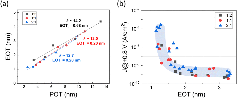
The results from electrical measurements closely corroborate the findings from the microstructural analyses. Fig. 6 illustrates the electrical measurement results for MIM devices fabricated with BMO films of varying thicknesses. The bulk k for each BMO film, based on cycle ratios of 1:2, 1:1, and 2:1, was determined through the inverse slope of the equivalent oxide thickness (EOT)–physical oxide thickness (POT) plot depicted in Fig. 6(a), where EOT was derived from the estimated k value of each sample by EOT = (3.9/k) × POT. For these cycle ratios, the k values were 14.2, 12.0, and 12.7. Given that the known k values for single films of MgO and BeO are 9.4 and 6.9, respectively,17,36 these results substantiate the hypothesis that forming a solid solution of MgO and BeO in BMO films enhances the dielectric constant.
 | ||
| Fig. 6 Plots illustrating the electrical characteristics of BMO-based metal–insulator–metal (MIM) devices: (a) equivalent oxide thickness (EOT) versus physical oxide thickness (POT) plot. (b) Leakage current density (J) versus EOT plot. | ||
Additionally, the y-axis intercept of the fitted line represents the interfacial EOT (EOTi), a factor potentially restricting EOT scaling in MIM devices.47 Values of EOTi less than 1 nm indicate a high-quality interface between the TiN electrodes and the BMO film, corroborating earlier discussions. Tangent loss values, derived from C–V measurements, consistently remained well below 0.1 for all samples, as further detailed in Fig. 7(b). This precludes the possibility that the elevated k values observed are a consequence of dielectric relaxation phenomena.
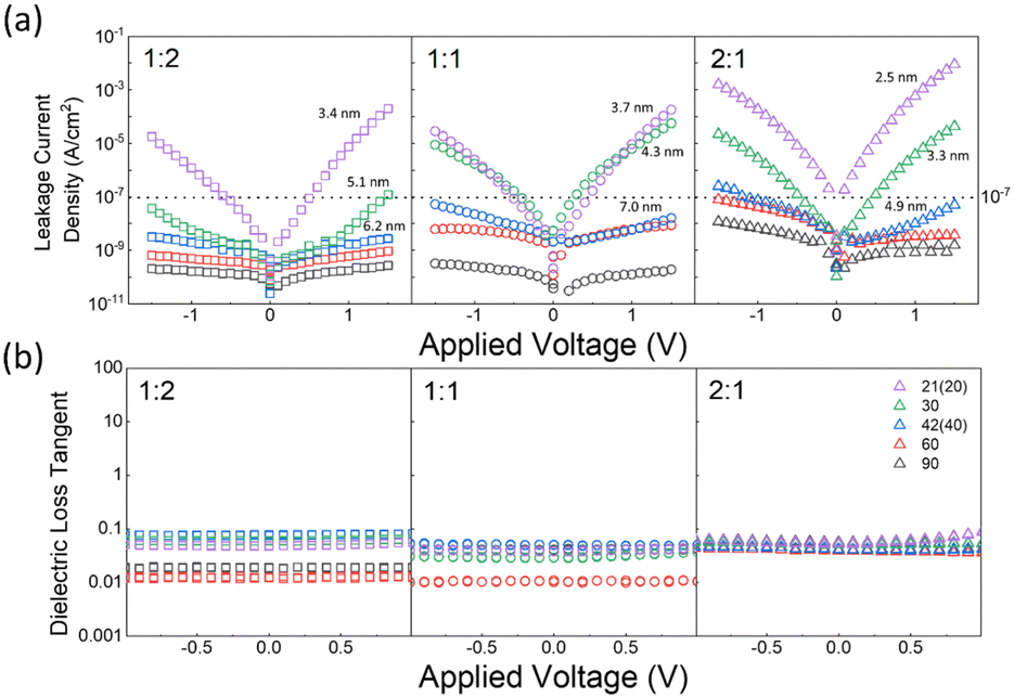 | ||
| Fig. 7 Electrical characterization of BMO-based metal–insulator–metal (MIM) devices, showing (a) current density–voltage (J–V) curves, and (b) dielectric loss tangent plots. These measurements are for devices with various total ALD cycle counts: 90, 60, 42 (40 for the 1:1 ratio), 30, and 21 (20 for the 1:1 ratio). The thicknesses of the three thinnest BMO films in each case are noted in (a). | ||
These results align with observations from GIXRD (Fig. 4) and TEM (Fig. 5). The 1:2 sample with the Be-content of 29% showed the highest k value of 14.2 among the three composition samples, indicating the RS structure of this sample. In the other two samples, although a certain amount of Be was incorporated into the RS MgO, there were regions where this incorporation was incomplete, resulting in a less pronounced increase in k value (12.0 and 12.7). These values were lower than those predicted by computational simulations and previous experimental research.37 This discrepancy may stem from the reduced thickness of BMO films (2–14 nm) used for this study compared to prior work (7–27 nm).
Fig. 6(b) shows a J–EOT plot that gauges the capacitor performance of the MIM devices under study. A critical J value of 10−7 A cm−2 at a +0.8 V bias was indicated, a standard criterion for DRAM capacitor operation. Samples with an EOT of 1.5 nm or higher (physical oxide thickness, POT ≥ 5 nm) displayed sufficiently low J levels. However, as the EOT decreases below 1.5 nm, a rapid increase in J value is observed. The minimum EOT within the standard leakage current specification was 1.30 nm (with J ∼ 1.8 × 10⁻⁸ A cm−2). Considering that the minimum EOT reported for MgO and BeO in earlier studies hovered around 3 nm,40,41 it is evident that utilizing a BeO–MgO solid solution film deposited through super-cycle ALD brings beneficial enhancements in electrical performances.
In contrast to the bulk k values derived from the EOT–POT relationship (Fig. 6(a)), the overall electrical performance shown in the J–EOT plot (Fig. 6(b)) appeared consistent across all compositions. Notably, all samples exhibited a common inverse relationship between the J level and the EOT, as indicated by the blue curve in the plot. In Be-rich samples, three different structures, RS, WZ, and amorphous, were observed, each with significantly different k values (approximately ∼12–18 for RS, ∼7 for WZ, and ∼6 for amorphous). The regions with lower k structures, such as WZ and amorphous, are expected to contribute positively to the J performance because dielectrics with lower k values generally exhibit stronger bonding strength and, consequently, higher bandgap energy. Therefore, the decrease in k value observed in Be-rich samples can be offset by reducing the POT, which lowers the EOT while maintaining optimal J performance.
Table 1 presents a comparative analysis of various MIM structures reported in the literature, including this study. This comparison focuses on the POT, EOT, and k values for devices that meet the standard criterion for critical J value (10−7 A cm−2 at 0.8 V). These parameters are pivotal in assessing their suitability for DRAM capacitor applications. Although BMO films exhibit a lower dielectric constant than other high-k materials, resulting in EOT values above 1 nm, their significant advantage is the substantially lower POT. These characteristics highlight BMO's potential in applications requiring ultra-thin dielectric films.
Another beneficial feature of BMO revealed in this research is the stable leakage current density and low dielectric loss values in MIM devices, even with sub-5 nm film thickness. The extremely narrow gap between the storage nodes of current DRAM requires dielectric film thickness (POT) <5 nm, irrespective of its electrical performance. Otherwise, the three-dimensional DRAM capacitor cannot be fabricated. Fig. 7(a) presents the J–V curves for MIM devices fabricated with various BMO film thicknesses, with the three thinnest samples in each case detailed in the figure. Correspondingly, Fig. 7(b) depicts the dielectric loss for these samples, using the same symbols and colors as in Fig. 7(a). Even for the thinnest 2.5 nm sample with a cycle ratio of 2:1 (total cycle number of 21), stable leakage current density was observed in the working voltage region, along with a dielectric loss value of ∼0.1. This low-level dielectric loss and stability in ultra-thin films, as corroborated by the consistent EOT–POT relationship in Fig. 6, are especially relevant for the advancement of DRAM capacitors, which require dielectric films to approach a thickness of 3 nm in line with ∼10 nm design rules. To the authors’ knowledge, no high-k dielectric material has been reported to exhibit such sufficiently low leakage currents at this thickness.
Fig. 8(a) provides the XPS valence band edge spectra for the BMO samples, using the Si substrate spectrum as a reference. All BMO samples exhibited a consistent valence band offset (VBO) value of 2.9 eV. Assuming a bandgap consistent with previous studies (>8 eV), the conduction band offset (CBO) would be greater than 5.1 eV. Although this value may involve uncertainty, it suggests a high likelihood of tunneling conduction mechanisms in ultra-thin (∼3 nm) layers with such high CBO values.
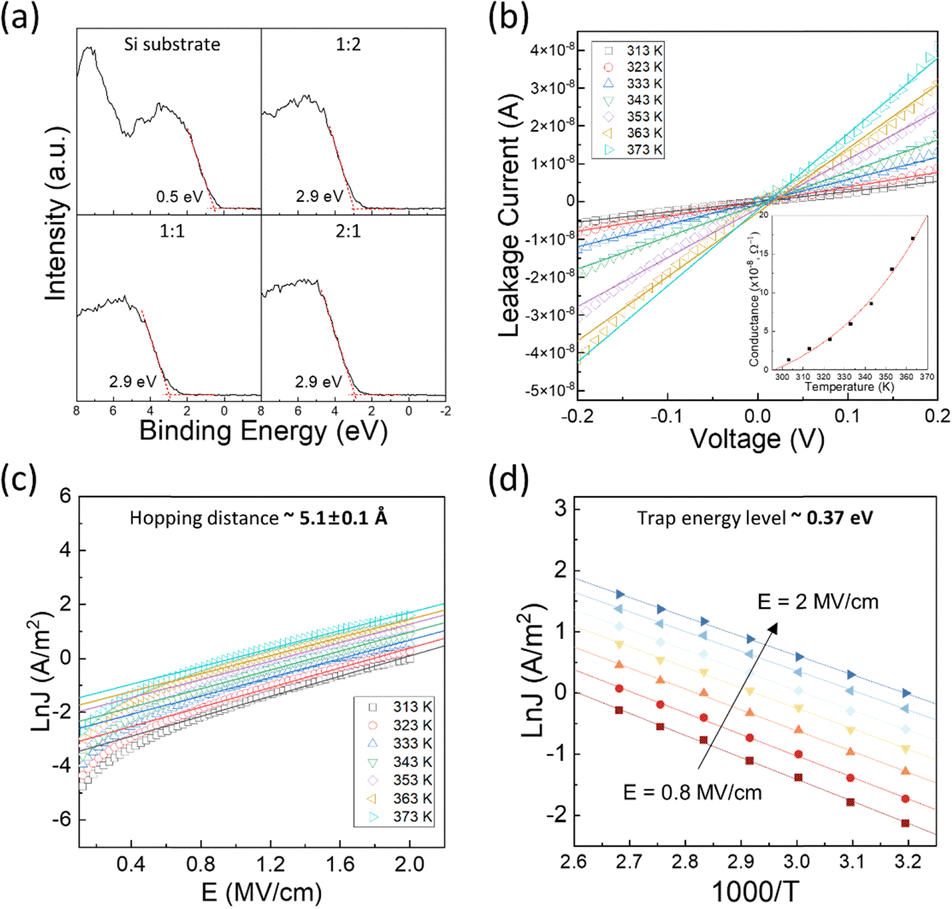 | ||
| Fig. 8 (a) XPS valence band edge spectra of BMO samples with the Si substrate spectrum included for comparison. (b) Leakage current measurements at various temperatures for a 3.3 nm thick BMO MIM sample with a cycle ratio of 2:1; conductance near 0 V is shown in the inset. (c) lnJ – E curve fitting for the hopping conduction model. (d) Arrhenius plot derived from lnJ – 1000/T data, focusing on the electric field region where linear fitting was applied. | ||
Therefore, the leakage current mechanisms were further investigated in a 3.3 nm-thick, 2:1 BMO film by measuring J–V curves with increasing temperatures. Conductance was calculated via the best linear fit of the J–V curve near 0 V. As shown in the inset of Fig. 8(b), temperature-dependent conductance indicates a lower likelihood of direct tunneling. Instead, the power function-like dependence of conductivity on temperature suggests the possibility of phonon-assisted tunneling, as outlined by the Glazman–Metrov model.51,52 However, an adequate fit could not be achieved for this case. Alternatively, trap-assisted tunneling (TAT) was examined, and the data could be well fitted using this model with appropriate parameters.
Fig. 8(c) and (d) present the results of fitting to the TAT model,53–55 represented by the equation 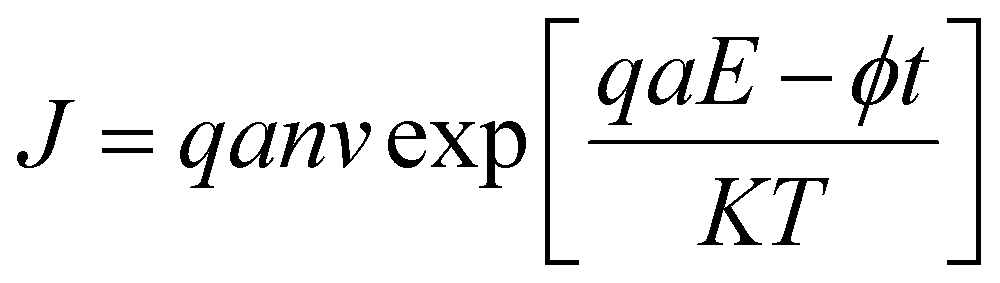 , where q is the electronic charge, a is the mean spacing between trap sites (i.e., the hopping distance), n is the electron concentration in the conduction band of the dielectric, v is the frequency of thermal vibration of electrons at the trap sites, T is the absolute temperature, K is the Boltzmann's constant, qaE is the field-effect barrier lowering, and ϕt is the energy level from the trap states to the bottom of the conduction band in BMO. The hopping distance was calculated from the slope of the ln(J)–E (electric field) curve in the E regions of 0.8–2 mV cm−1, while the trap energy level was derived from the slopes of the Arrhenius plot of ln(J)–1000/T. The estimated hopping distance is approximately 5.1 Å, with a trap energy of 0.37 eV. These values agree well with previously reported values of 6.6 Å for hopping distance and 0.22 eV for trap energy level in thermally grown ALD MgO films.56 The conduction via the TAT mechanism could be sustained up to a high electric field of 2 mV cm−1 without breakdown, which can be attributed to the robust dielectric strength of the BMO layer.
Lastly, the stability of BMO films over the humidity was investigated by examining changes in electrical properties over time following MIM fabrication. Fig. 9 displays the J–V and C–V measurement results before and after the elapsed time of up to 9 months in the atmosphere, represented by black and red dots. Degradations are mainly observed in Mg-rich samples, while Be-rich samples exhibit relatively higher resistance to degradation. These degradations are believed to arise from the well-known hygroscopic nature of MgO.39 When MgO comes into contact with moisture, it forms Mg(OH)2, decreasing capacitance due to its dissolution into cations and anions. The relative water resistance of Be-rich BMO films presents a potential solution for adopting hygroscopic MgO-based films in integrated circuit fabrication. However, further study is necessary to determine the specific relationship between changes in film microstructure and their impact on electrical properties.
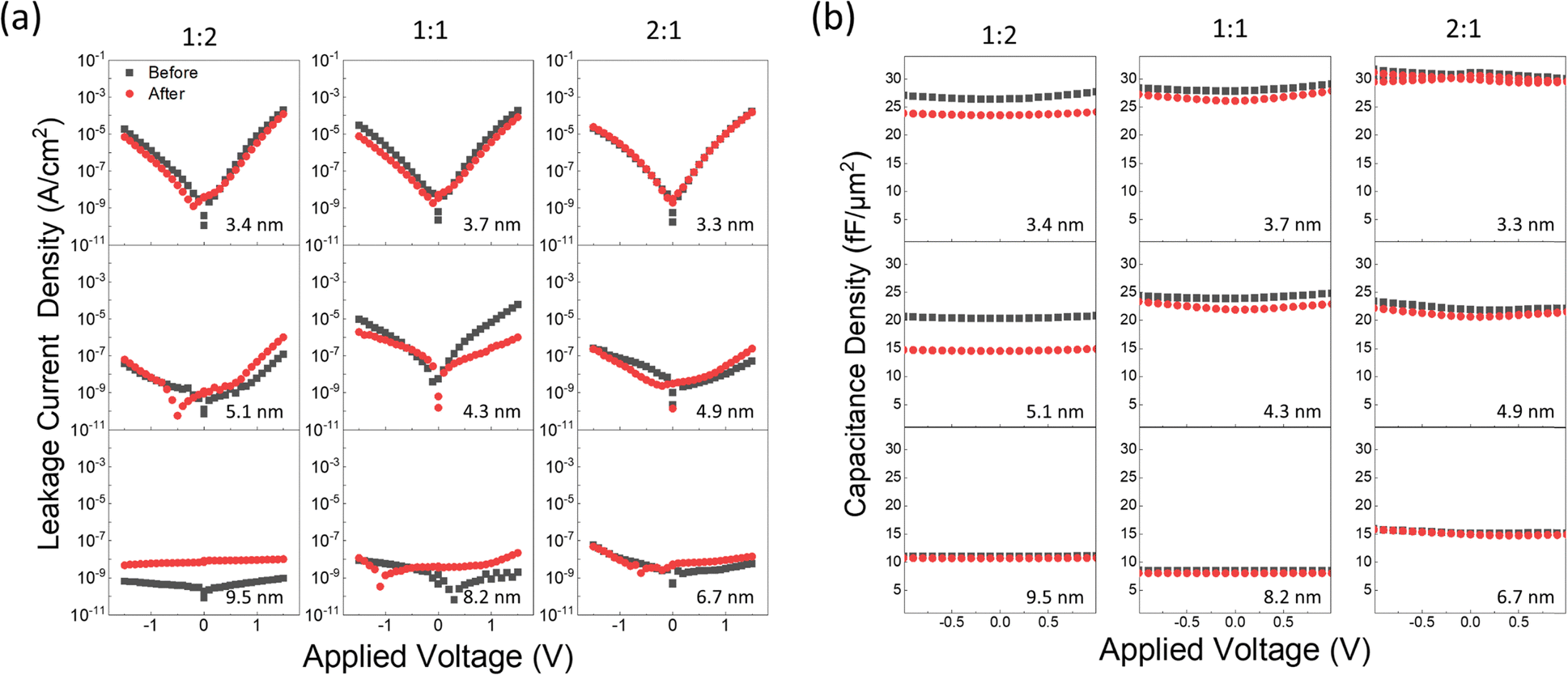 | ||
| Fig. 9 Long-term stability assessment of BMO-based metal–insulator–metal (MIM) devices conducted over a period of 9 months. (a) J–V plots illustrating changes in leakage current performance over time, and (b) C–V plots demonstrating the variations in capacitance before and after the elapsed period. | ||
Previous research that adopted laminated BeO/MgO/BeO films for water stability enhancement discussed the path for water diffusion.41 In that case, it was assumed that degradation occurred partially near the interface between the dielectric layer and the top electrode. In the present study, the degradation of J–V was more prominent in thicker samples. In cases showing well-controlled low J levels, as seen in thick samples, creating new leakage paths due to interfacial degradation has a more detrimental impact than in cases where J levels were initially high, as in thin samples. Conversely, the degradation of C–V was more prominent in thinner samples. The proportion of degraded thickness relative to the total dielectric thickness is higher for thinner samples, resulting in a more pronounced decrease in capacitance than in thicker samples.
Conclusions
In conclusion, this study reports a detailed investigation of the fabrication and characterization of BMO thin films using super-cycle ALD for the high-k dielectric application. Super-cycle ALD, adopting the O3 instead of H2O as the oxygen source, suppressed abnormal overgrowth of the MgO film and carbon fragment inclusion into the film. This suppression is derived from the small size of the DEBe precursor, which can facilitate the ALD-specific ligand exchange reaction at the reaction sites. Microstructural analyses showed that the BMO film with <∼30% Be-content had an RS structure. However, the film contained a WZ structure portion as the Be-content exceeded ∼30%. Nonetheless, the RS phase remains dominant even in films with higher Be content, owing to the structural coherency between MgO and TiN. This coherency is further facilitated by the layer-by-layer growth mode inherent to ALD, enabling the BMO films to inherit the crystalline structure of the underlying TiN layer.The films exhibited promising electrical performance, achieving a minimum EOT of 1.30 nm while securing the DRAM capacitor leakage current specification. Moreover, stable leakage current density and low dielectric loss were observed even at a film as thin as 2.5 nm, with current conduction predominantly occurring through the TAT model over a large electric field region. These traits are particularly advantageous for DRAM capacitors, where ultra-thin dielectric layers are necessary. Also, Be-rich BMO samples displayed enhanced resistance to water-induced degradation, establishing them as potential candidates for integration into circuit designs.
Author contributions
H. Song designed and performed the experiments and wrote the manuscript draft. B. Wang assisted with the experiment design and data interpretations. J. Shin, Y. Park, T. K. Kim, H. Paik, H. Seo, J. Lim and D. Kwon helped review the manuscript. K. Lee, Y. S. Kim and D. H. Shin assisted with the ALD deposition and device fabrication. C. S. Hwang supervised the whole research and manuscript preparation.Conflicts of interest
There are no conflicts to declare.Acknowledgements
This work was supported by the Korea Evaluation Institute of Industrial Technology through the Technology Innovation Program (no. 20017216).Notes and references
- J. Robertson, J. Vac. Sci. Technol., B: Microelectron. Nanometer Struct. – Process., Meas., Phenom., 2000, 18, 1785–1791 CrossRef.
- S. K. Kim, S. W. Lee, J. H. Han, B. Lee, S. Han and C. S. Hwang, Adv. Funct. Mater., 2010, 20, 2989–3003 CrossRef.
- W. Jeon, J. Mater. Res., 2020, 35, 775–794 CrossRef.
- K. H. Kuesters, M. F. Beug, U. Schroeder, N. Nagel, U. Bewersdorff, G. Dallmann, S. Jakschik, R. Knoefler, S. Kudelka, C. Ludwig, D. Manger, W. Mueller and A. Tilke, Adv. Eng. Mater., 2009, 11, 241–248 CrossRef.
- D.-S. Kil, K. Hong, K.-J. Lee, J. Kim, H.-S. Song, K.-S. Park, J.-S. Roh, H.-C. Sohn, J.-W. Kim and S.-W. Park, in Digest of Technical Papers. 2004 Symposium on VLSI Technology, 2004., 2004, pp. 126–127.
- M. H. Park, Y. H. Lee, T. Mikolajick, U. Schroeder and C. S. Hwang, MRS Commun., 2018, 8, 795–808 CrossRef.
- D.-S. Kil, H.-S. Song, K.-J. Lee, K. Hong, J.-H. Kim, K.-S. Park, S.-J. Yeom, J.-S. Roh, N.-J. Kwak, H.-C. Sohn, J.-W. Kim and S.-W. Park, in 2006 Symposium on VLSI Technology, 2006. Digest of Technical Papers., 2006, pp. 38–39.
- H. J. Cho, Y. D. Kim, D. S. Park, E. Lee, C. H. Park, J. S. Jang, K. B. Lee, H. W. Kim, Y. J. Ki, I. K. Han and Y. W. Song, Solid-State Electron., 2007, 51, 1529–1533 CrossRef.
- H. Seo, I. W. Yeu, D. S. Kwon, D. G. Kim, J. Lim, T. K. Kim, H. Paik, J.-H. Choi and C. S. Hwang, Adv. Electron. Mater., 2022, 8, 2200099 CrossRef.
- S. H. Cha, C. H. An, S. T. Cho, D.-G. Kim, D. S. Kwon, J. I. Lim, W. Jeon and C. S. Hwang, Phys. Status Solidi RRL, 2019, 13, 1900282 CrossRef.
- S. K. Kim, W. D. Kim, K. M. Kim, C. S. Hwang and J. Jeong, Appl. Phys. Lett., 2004, 85, 4112–4114 CrossRef.
- S. K. Kim, G.-J. Choi, S. Y. Lee, M. Seo, S. W. Lee, J. H. Han, H.-S. Ahn, S. Han and C. S. Hwang, Adv. Mater., 2008, 20, 1429–1435 CrossRef.
- S. K. Kim, K. M. Kim, D. S. Jeong, W. Jeon, K. J. Yoon and C. S. Hwang, J. Mater. Res., 2013, 28, 313–325 CrossRef.
- S. W. Lee, J. H. Han, S. Han, W. Lee, J. H. Jang, M. Seo, S. K. Kim, C. Dussarrat, J. Gatineau, Y.-S. Min and C. S. Hwang, Chem. Mater., 2011, 23, 2227–2236 CrossRef.
- W. Lee, J. H. Han, W. Jeon, Y. W. Yoo, S. W. Lee, S. K. Kim, C.-H. Ko, C. Lansalot-Matras and C. S. Hwang, Chem. Mater., 2013, 25, 953–961 CrossRef.
- S. H. Kim, W. Lee, C. H. An, Y. Kim, D. S. Kwon, D.-G. Kim, S. H. Cha, S. T. Cho, J. Lim and C. S. Hwang, Phys. Status Solidi RRL, 2019, 13, 1900373 CrossRef.
- M. A. Subramanian, R. D. Shannon, B. H. T. Chai, M. M. Abraham and M. C. Wintersgill, Phys. Chem. Miner., 1989, 16, 741 CrossRef.
- D. M. Roessler, W. C. Walker and E. Loh, J. Phys. Chem. Solids, 1969, 30, 157–167 CrossRef.
- G. A. Slack and S. B. Austerman, J. Appl. Phys., 1971, 42, 4713–4717 CrossRef.
- S. C. Carniglia and J. E. Hove, J. Nucl. Mater., 1961, 4, 165–176 CrossRef.
- S. B. Austerman, J. Nucl. Mater., 1964, 14, 225–236 CrossRef.
- U. D. Wdowik, J. Phys.: Condens. Matter, 2010, 22, 045404 CrossRef.
- W. A. Chupka, J. Berkowitz and C. F. Giese, J. Chem. Phys., 2004, 30, 827–834 CrossRef.
- G. G. Bentle, J. Am. Ceram. Soc., 1966, 49, 125–128 CrossRef.
- C. F. Cline, H. L. Dunegan and G. W. Henderson, J. Appl. Phys., 2004, 38, 1944–1948 CrossRef.
- R. M. Hazen and L. W. Finger, J. Appl. Phys., 1986, 59, 3728–3733 CrossRef.
- V. Milman and M. C. Warren, J. Phys.: Condens. Matter, 2001, 13, 241 CrossRef.
- I. R. Shein, V. S. Kiĭko, Yu. N. Makurin, M. A. Gorbunova and A. L. Ivanovskiĭ, Phys. Solid State, 2007, 49, 1067–1073 CrossRef.
- V. A. Sashin, M. A. Bolorizadeh, A. S. Kheifets and M. J. Ford, J. Phys.: Condens. Matter, 2003, 15, 3567 CrossRef.
- K. J. Hubbard and D. G. Schlom, J. Mater. Res., 1996, 11, 2757–2776 CrossRef.
- K. Yim, Y. Yong, J. Lee, K. Lee, H.-H. Nahm, J. Yoo, C. Lee, C. Seong Hwang and S. Han, NPG Asia Mater., 2015, 7, e190–e190 CrossRef.
- J. Boettger and J. Wills, Phys. Rev. B: Condens. Matter Mater. Phys., 1996, 54, 8965–8968 CrossRef PubMed.
- C. Park, S. Lee, Y. Ko and K. J. Chang, Phys. Rev. B: Condens. Matter Mater. Phys., 1999, 59, 13501–13504 CrossRef.
- M. B. Sahariah and S. Ghosh, J. Appl. Phys., 2010, 107, 083520 CrossRef.
- A. P. Jephcoat, R. J. Hemley, H. K. Mao, R. E. Cohen and M. J. Mehl, Phys. Rev. B: Condens. Matter Mater. Phys., 1988, 37, 4727–4734 CrossRef PubMed.
- L. Yan, C. M. Lopez, R. P. Shrestha, E. A. Irene, A. A. Suvorova and M. Saunders, Appl. Phys. Lett., 2006, 88, 142901 CrossRef.
- W. C. Lee, S. Kim, E. S. Larsen, J. H. Choi, S. H. Baek, M. Lee, D. Y. Cho, H. K. Lee, C. S. Hwang, C. W. Bielawski and S. K. Kim, Appl. Surf. Sci., 2020, 501, 144280 CrossRef.
- G. Han, I. W. Yeu, K. H. Ye, S.-C. Lee, C. S. Hwang and J.-H. Choi, J. Mater. Chem. C, 2021, 9, 851–859 RSC.
- J. H. Lee, J. H. Eun, S. G. Kim, S. Y. Park, M. J. Lee and H. J. Kim, J. Mater. Res., 2003, 18, 2895–2903 CrossRef CAS.
- B. W. Wang, J. Choi, H. G. Kim, S. D. Hyun, C. Yoo, S. Kim, H. Lee and C. S. Hwang, J. Mater. Chem. C, 2021, 9, 15359–15374 RSC.
- B. W. Wang, S. Kim, H. Song, H. Seo, X. Li, J. M. Choi, J. Choi, J. Shin and C. S. Hwang, J. Mater. Chem. C, 2022, 10, 6611–6620 RSC.
- D. Koh, J.-H. Yum, S. K. Banerjee, T. W. Hudnall, C. Bielawski, W. A. Lanford, B. L. French, M. French, P. Henry, H. Li, M. Kuhn and S. W. King, J. Vac. Sci. Technol., B: Microelectron. Nanometer Struct. – Process., Meas., Phenom., 2014, 32, 03D117 CrossRef.
- J. L. Chen and J. H. Zhu, Res. Chem. Intermed., 2019, 45, 947–950 CrossRef CAS.
- Y. Jang, D. Jung, P. R. Sultane, E. S. Larsen, C. W. Bielawski, S. M. Lee and J. Oh, Appl. Surf. Sci., 2021, 572, 151405 CrossRef.
- W. Olovsson, L. Weinhardt, O. Fuchs, I. Tanaka, P. Puschnig, E. Umbach, C. Heske and C. Draxl, J. Phys.: Condens. Matter, 2013, 25, 315501 CrossRef CAS.
- S. M. Lee, J. H. Yum, S. Yoon, E. S. Larsen, W. C. Lee, S. K. Kim, S. Shervin, W. Wang, J.-H. Ryou, C. W. Bielawski and J. Oh, ACS Appl. Mater. Interfaces, 2017, 9, 41973–41979 CrossRef CAS.
- S. E. Kim, J. Y. Sung, J. D. Jeon, S. Y. Jang, H. M. Lee, S. M. Moon, J. G. Kang, H. J. Lim, H.-S. Jung and S. W. Lee, Adv. Mater. Technol., 2023, 8, 2200878 CrossRef CAS.
- W. Jeon, S. Yoo, H. K. Kim, W. Lee, C. H. An, M. J. Chung, C. J. Cho, S. K. Kim and C. S. Hwang, ACS Appl. Mater. Interfaces, 2014, 6, 21632–21637 CrossRef CAS.
- Y. W. Kim, A. J. Lee, D. H. Han, D. C. Lee, J. H. Hwang, Y. Kim, S. Moon, T. Youn, M. Lee and W. Jeon, J. Mater. Chem. C, 2022, 10, 12957–12965 RSC.
- S. Kupke, S. Knebel, U. Schroeder, S. Schmelzer, U. Bottger and T. Mikolajick, IEEE Electron Device Lett., 2012, 33, 1699–1701 CAS.
- B. Oliver and J. Nowak, J. Appl. Phys., 2003, 95, 546–550 CrossRef.
- Z. Wen, L. You, J. Wang, A. Li and D. Wu, Appl. Phys. Lett., 2013, 103, 132913 CrossRef.
- F.-C. Chiu, W.-C. Shih and J.-J. Feng, J. Appl. Phys., 2012, 111, 094104 CrossRef.
- F.-C. Chiu, Adv. Mater. Sci. Eng., 2014, 2014, 578168 Search PubMed.
- F.-C. Chiu, P.-W. Li and W.-Y. Chang, Nanoscale Res. Lett., 2012, 7, 1–9 CrossRef PubMed.
- W. Kang, B. J. Choi and J. H. Han, Ceram. Int., 2020, 46, 10115–10120 CrossRef CAS.
Footnote |
| † Electronic supplementary information (ESI) available: AES depth profiles of BMO samples with different cycle ratios. See DOI: https://doi.org/10.1039/d3tc04338j |
| This journal is © The Royal Society of Chemistry 2024 |