
 Open Access Article
 This Open Access Article is licensed under a
 Creative Commons Attribution 3.0 Unported Licence
From monolayer to thin films: engineered bandgap in CVD grown Bi2Se(3−x)Sx topological insulator alloys†
Michal
Poplinger
ab,
Dimitris
Kaltsas
 c,
Chen
Stern
ab,
Pilkhaz
Nanikashvili
ab,
Adi
Levi
ab,
Rajesh K.
Yadav
ab,
Sukanta
Nandi
ab,
Yuxiao
Wu
bd,
Avinash
Patsha
e,
Ariel
Ismach
e,
Ashwin
Ramasubramaniam
fg,
Amaia
Pesquera
h,
Amaia
Zurutuza
h,
Ioanna
Zergioti
c,
Leonidas
Tsetseris
c,
Tomer
Lewi
ab and
Doron
Naveh
*ab
c,
Chen
Stern
ab,
Pilkhaz
Nanikashvili
ab,
Adi
Levi
ab,
Rajesh K.
Yadav
ab,
Sukanta
Nandi
ab,
Yuxiao
Wu
bd,
Avinash
Patsha
e,
Ariel
Ismach
e,
Ashwin
Ramasubramaniam
fg,
Amaia
Pesquera
h,
Amaia
Zurutuza
h,
Ioanna
Zergioti
c,
Leonidas
Tsetseris
c,
Tomer
Lewi
ab and
Doron
Naveh
*ab
aFaculty of Engineering, Bar-Ilan University, Ramat-Gan 52900, Israel. E-mail: doron.naveh@biu.ac.il
bInstitute for Nanotechnology and Advanced Materials, Bar-Ilan University, Ramat-Gan 52900, Israel
cDepartment of Physics, School of Applied Mathematical and Physical Sciences, National Technical University of Athens, Athens, Greece
dDepartment of Physics, Faculty of Exact Sciences, Bar-Ilan University, Ramat-Gan 52900, Israel
eDepartment of Materials Science and Engineering, Tel Aviv University, Ramat Aviv, Tel Aviv 6997801, Israel
fDepartment of Mechanical and Industrial Engineering, University of Massachusetts, Amherst, USA
gMaterials Science and Engineering Graduate Program, University of Massachusetts, Amherst, USA
hGraphenea Headquarters, Spain
First published on 17th January 2024
Abstract
Topological insulators, a class of materials possessing bulk bandgap and metallic surface states with a topological nontrivial symmetry, are considered promising candidates for emerging quantum and optoelectronic applications. However, achieving scalable growth and control over the parameters including thickness, carrier density, bulk bandgap, and defect density remains a challenge in realizing such applications. In this work, we show the scalable growth of topological insulator alloys Bi2Se(3−x)Sx and demonstrate composition-tunable bandgap, using chemical vapor deposition (CVD). A bandgap increase of up to ∼40% at a sulfur concentration of ∼15% is demonstrated. Correspondingly, the real part (n) of the refractive index is reduced in the alloy by ∼25% relative to that of Bi2Se3. Additionally, electronic transport measurements indicate a bulk p-type doping and field-effect tunable metallic surface states of the alloy. This work paves the way for the controlled growth of topological insulators, free from surface-state pinning, suitable for quantum optoelectronics and spintronics applications.
Introduction
Topological insulators (TIs), a class of materials having a bulk bandgap and metallic states,1–4 are considered promising for novel applications in electronics and optoelectronics.5–10 This is due to the several interesting properties introduced by their surface/edge states such as spin-momentum locking, resulting in spin-polarized transport and significant suppression of backscattering by impurities.11 The topological properties are mainly induced by relatively strong spin–orbit coupling interaction,12,13 and under certain conditions, may also be augmented by applying an electric field.12Bi2Se3 is one of the most studied three-dimensional (3D) TIs due to its ![[Doublestruck Z]](https://www.rsc.org/images/entities/char_e17d.gif) 2 topology manifested in a band structure with a single Dirac cone at the gamma point and a relatively large, direct bandgap of ∼0.3 eV.11,14–17 However, the material is usually heavily n-doped, likely due to shallow defect states emerging from Se vacancies that act as donors. This results in the pinning of the Fermi level to the conduction band, leading to bulk conduction rather than surface-dominated conduction of charge carriers. This issue is one of the main challenges in device applications of Bi2Se3 and other TIs.11,14,15,18
2 topology manifested in a band structure with a single Dirac cone at the gamma point and a relatively large, direct bandgap of ∼0.3 eV.11,14–17 However, the material is usually heavily n-doped, likely due to shallow defect states emerging from Se vacancies that act as donors. This results in the pinning of the Fermi level to the conduction band, leading to bulk conduction rather than surface-dominated conduction of charge carriers. This issue is one of the main challenges in device applications of Bi2Se3 and other TIs.11,14,15,18
The pursuit of TI materials having large bulk bandgaps also stems from their importance for future room-temperature spintronic applications.1,19,20 In this respect, alloying presents a promising means of tuning the electronic properties of Bi2Se3,15,21–23 with the potential to address both the problems of Fermi-level pinning and bandgap engineering. By utilizing a chemical composition of higher stability in the alloy, the density of natural chalcogen vacancies decreases and suppresses the natural n-doping of Bi2Se3.
The implementation of practical electronic and optoelectronic devices requires repeatable growth of high-quality active materials with uniformity over large areas. In this context, chemical vapor deposition (CVD) is a well-known method for scalable deposition of transition metal dichalcogenides (TMDCs),24,25 transition metal oxides (TMOs) such as wafer-scale single-layer amorphous MoO3,26,27 and has also been demonstrated on chalcogenide optical materials.28 CVD grown Bi2Se3 crystals, with sizes up to 20 μm, were previously reported as well,29 yet the synthesis of alloyed Bi2Se3 has primarily relied on solution-processed techniques and molecular beam epitaxy (MBE).15,21,30–32
Here, we show a CVD growth of Bi2Se3 alloyed with sulfur on various substrates, from isolated crystals to continuous films, uniform on a wafer-scale and with a crystal domain size up to ∼50 μm. The alloyed crystals present a wider bulk bandgap (up to 40% larger than pure Bi2Se3), p-type doping, and field-effect tunable Fermi-level while maintaining the original structural and topological properties of Bi2Se3.
Results and discussion
Continuous layers and isolated Bi2Se(3−x)Sx crystals were grown by CVD on various substrates (see Table 1), starting from Bi2Se3 powder (Alfa Aesar – 99.999%) and sulfur powder (Sigma Aldrich – 99.5%), as illustrated schematically in Fig. 1a. In short, the growth of Bi2Se(3−x)Sx was carried out in a quartz tube at the temperatures specified in Table 1 for the Bi2Se3 precursor and at 140 °C for the sulfur, at a base pressure of 50 mTorr and N2 flow rate of 5 sccm (see the ESI† for full synthesis details). The temperature of the substrate (Table 1) was controlled by its distance from the Bi2Se3 precursor and the temperature at the center of the furnace.| Substrate | Growth temperature [°C] | Growth time [min.] | Substrate temperature [°C] | Morphology |
|---|---|---|---|---|
| Si/SiO2 | 570 | 10 | 440 | Isolated hexagonal crystals with growth direction perpendicular to the substrate (Fig. S1a, ESI) |
| Sapphire | 580 | 180 | 450 | Hexagonal crystals on a scale of ∼50 μm clustered in vertical growth (Fig. S1b, ESI) |
| Monolayer graphene on Si/SiO2 | 580 | 60 | 460 | Isolated hexagonal crystals on a scale of up to 15 μm (Fig. S1c, ESI) |
| 120 | 440 | Isolated hexagonal crystals on a scale of up to 20 μm (Fig. S1d, ESI) | ||
| 180 | 410 | Continuous layers (Fig. S1e, ESI) |
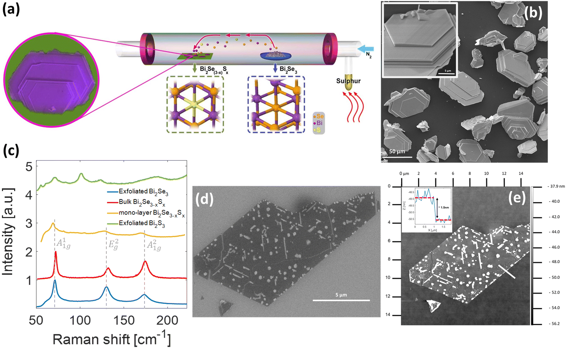 | ||
| Fig. 1 Growth process and structural characterization of CVD-grown Bi2Se(3−x)Sx. (a) Schematic illustration of the CVD system and growth process. (b) HRSEM images of the hexagonal grown Bi2Se(3−x)Sx crystals. (c) Raman spectra of exfoliated Bi2Se3 (blue), bulk and monolayer Bi2Se(3−x)Sx grown by CVD (red and yellow respectively), and exfoliated Bi2S3 (green). (d) HRSEM image of monolayer Bi2Se(3−x)Sx grown by CVD. (e) AFM topography of monolayer Bi2Se(3−x)Sx grown by CVD, showing (inset) a 1.5 nm step thickness of the flake. | ||
The representative morphology of isolated crystals is presented in Fig. 1b, showing hexagonal domains on a scale of up to 50 μm. However, the morphology depends drastically on the growth substrate and exhibits large variations in the growth products. On a substrate of Si/SiO2, the hexagonal crystals are oriented vertically to the surface, having minimal contact area with the substrate (Fig. S1a, ESI†). On sapphire substrates, multiple crystalline domains grow laterally and vertically from a single seed and overlap each other (Fig. S1b, ESI†). In high-vacuum conditions, the growth is dominated by thin crystals and adlayers forming crystal seeds in the principal crystalline directions. The minimal measured thickness is attributed to such a monolayer and was found to be 1.5 nm (see the SEM micrograph and AFM topography in Fig. 1d and e). Interestingly, the growth on graphene-covered Si/SiO2 is lateral (Fig. S1c and S1d, ESI†) and tends to form continuous films (Fig. S1e, ESI†). The latter is probably a result of reduced surface reactivity and enhanced diffusivity of the reactants on the surface of graphene. In all cases, the obtained alloys maintain high uniformity (Fig. 2 and Fig. S2, ESI†), owing to the high diffusivity of sulfur in Bi2Se3 and its ability to passivate existing vacancies (see Fig. S3 and associated text, ESI†).
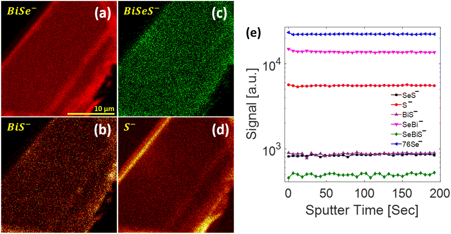 | ||
| Fig. 2 Time-of-flight secondary ion mass spectroscopy (TOF-SIMS) analysis. Chemical lateral imaging of Bi2Se(3−x)Sx flakes using (a) BiSe−, (b) BiS−, (c) BiSeS−, and (d) S− ions. (e) Signal intensity of selected ions as a function of sputtering time (depth). | ||
The Raman signature (Fig. 1c) of bulk and monolayer Bi2Se(3−x)Sx (red and yellow lines, respectively) show similar peak positions, with distinct broadening of the peaks in the monolayer crystal compared to that of a bulk crystal. Both thin and thick alloys show shifted spectra relative to pure exfoliated Bi2Se3 (Fig. 1c, blue line), as specified in Table S1 (ESI†). The Raman spectrum of orthorhombic Bi2S3 (Fig. 1c, green line) differs distinctly from the rhombohedral crystals, showing characteristic Raman modes at ∼101 and ∼189 cm−1 that do not appear in the grown alloy materials. This is further supported by the X-ray diffraction (XRD) pattern of the alloyed samples in which the peaks show proximity to those of the reference exfoliated Bi2Se3 sample and agree with the calculated XRD of the rhombohedral structure (Fig. S4, ESI†).
From the analysis of XRD measurements of the alloyed crystals (Fig. 3a and Fig. S4b, ESI†), the variation in the c-axis spacing was correlated with structurally optimized results of Density Functional Theory (DFT) calculations resolved by relative sulfur concentration (see ESI† for details). In a random alloy, the calculated structure predicts a trend that can be fitted to c = −4 × 10⁻⁵[%S]2 − 6.5 × 10⁻³[%S] + 28.669 Å (Fig. S5, ESI†), where the constant coefficient (28.669) is the experimental c value for pure Bi2Se3. The data for two alloys on monolayer graphene on Si/SiO2 (90 nm) are summarized in Table 2 relative to Bi2Se3.
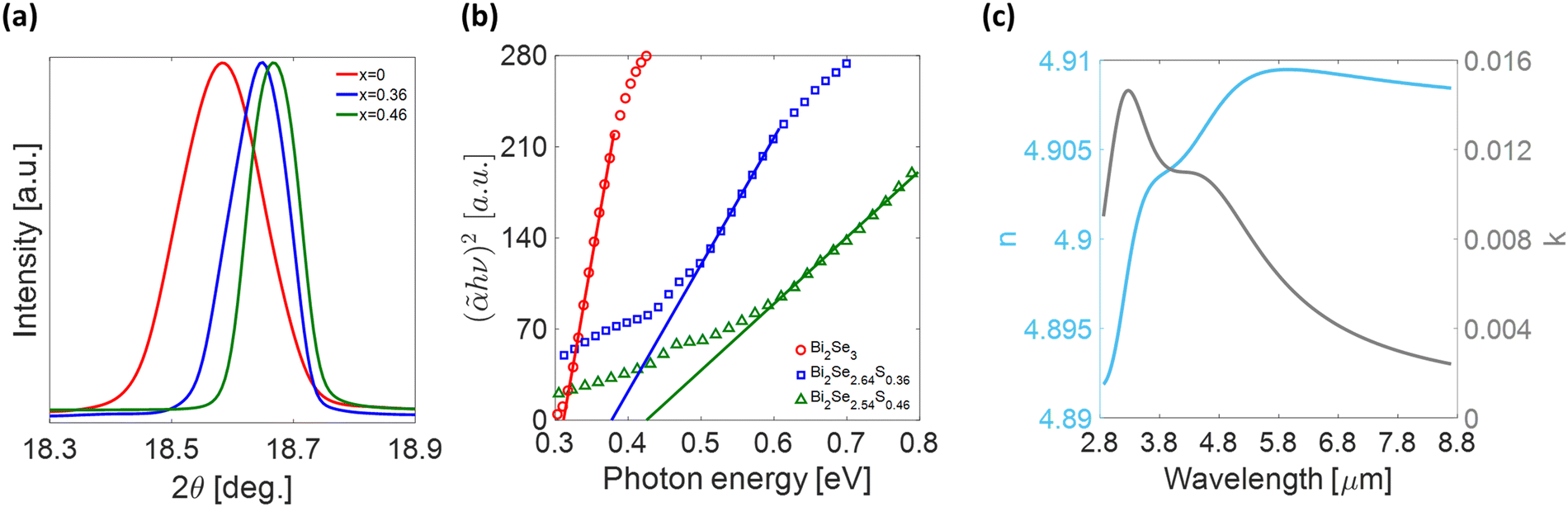 | ||
| Fig. 3 (a) Illustration of the shift in the crystallographic planes of the alloyed samples relative to those of Bi2Se3 (the crystallographic plane 006 is given as an example). (b) Tauc plots for the direct bandgap of exfoliated pure Bi2Se3 and sulfur alloyed Bi2Se3 samples. (c) Extracted real (n, blue line) and imaginary (k, gray line) parts of the refractive index of Bi2Se2.64S0.36. | ||
| Sample | c [Å] | [%S] | x | Chemical formula | E g [eV] |
|---|---|---|---|---|---|
| Bi2Se3 | 28.669 | 0 | 0 | Bi2Se3 | 0.31 ± 1.42 × 10⁻³ |
| Bi2Se(3−x)Sx #1 | 28.586 | 11.9 | 0.36 | Bi2Se2.64S0.36 | 0.38 ± 1.42 × 10⁻³ |
| Bi2Se(3−x)Sx #2 | 28.561 | 15.2 | 0.46 | Bi2Se2.54S0.46 | 0.43 ± 2.74 × 10⁻³ |
The variation in the bandgap values of these samples is given in Table 2. The values were determined by applying the Tauc method on the quantity ![[small alpha, Greek, tilde]](https://www.rsc.org/images/entities/i_char_e0dc.gif) , which was obtained by employing the Kubelka–Munk (K–M) function (eqn (1))33,34 on the reflection spectra of the samples:
, which was obtained by employing the Kubelka–Munk (K–M) function (eqn (1))33,34 on the reflection spectra of the samples:
 | (1) |
 is the reflection of the sample. Pure exfoliated Bi2Se3 yielded a direct bandgap of 0.31 eV (Fig. 3b), matching with the data reported in the literature for Bi2Se3. The calculated direct bandgap values of the alloyed samples are summarized in Table 2. Correlating the sulfur content with the calculated bandgaps, we find that the bandgap increases with higher sulfur content in the sample. Particularly, replacing 15.2% of the chalcogen content with sulfur results in a nearly 40% larger bandgap than that of Bi2Se3.
Fig. 3c shows the real (n) and imaginary (k) parts of the complex refractive index of Bi2Se2.64S0.36 obtained by fitting the experimental reflection spectrum with a multiple Drude–Lorentz oscillator model, as detailed in Fig. S6 and Table S2 (ESI†). The values of n at the wavelength corresponding to the bulk energy bandgap are compared for the pure (6.34)35 and alloyed (4.90) Bi2Se(3−x)Sx TIs and are qualitatively in compliance with the Moss relation (Table 3).36 However, the metallic surface states result in the absence of an absorption edge in TIs, rendering the Moss relation as undefined. In addition, in highly doped samples, where the Fermi level is pinned to the conduction band, a Moss–Burstein shift is manifested due to the metallicity of the bulk.37–39 Interestingly, the losses manifested in the imaginary part of the refractive index are significantly smaller than previously reported chalcogenide topological insulators.7,35,40
Further characterization of the alloy TIs was exercised by measuring their electrical characteristics. Devices were fabricated on 300 nm Si/SiO2 (Fig. 4a) with metallization of Ti/Au contacts. Room temperature I–V measurements at varying gate voltages show an effective field effect (Fig. 4b and c), with some nonlinear character arising from a metal-semiconductor interface at the contacts. This is indicative of an unpinned Fermi-level in the alloyed samples as well as a narrow bulk bandgap semiconductor rather than the metallic behavior of highly doped topological insulators. Furthermore, temperature-dependent measurements (see the ESI† for details) demonstrate a typical metallic behavior, where the resistance increases with increasing temperature (Fig. 4c inset), as opposed to a semiconductor. This characteristic metallic behavior stems from a decrease in the mean free path of electrons between collisions as temperature increases. Since the bulk of the alloys exhibits a bandgap that was measured optically, the metallic transport is exclusively attributed to surface states, implying that the topological phase is maintained after alloying with sulfur. Yet, the origin of the varying temperature coefficient of resistance remains unclear. Notably, monolayer samples are highly resistive, indicating that the topological phase is not supported in monolayer Bi2Se(3−x)Sx. We associate the electrical resistance with the contact interface; however, at this stage, these observations are not conclusive and may require further investigation.
 | ||
| Fig. 4 (a) Optical microscope image of a Bi2Se(3−x)Sx device. Gate-dependent (b) Id–Vd and (c) conductance of a Bi2Se(3−x)Sx device. Inset shows resistance as a function of the temperature of a Bi2Se(3−x)Sx device. | ||
Conclusions
We have grown Bi2Se(3−x)Sx by CVD from powder precursors on several substrates, obtaining isolated crystals and continuous films. The formation of the latter is promoted by graphene-covered substrates, probably due to enhanced diffusion and reduced surface chemical reactivity. Additionally, smaller Bi2Se(3−x)Sx crystals tend to have higher sulfur content (12–15%). We associate this trend with the increased surface area of smaller crystals, leading to higher sulfur diffusion. Optical measurements show that the bulk energy bandgap was tuned by ∼40% with a sulfur content of ∼15%, a reasonable value compared with, e.g., InGaAs.41 The bandgap tuning affected the optical constants and reduced the n value of Bi2Se2.64S0.36 by ∼25% compared to that of Bi2Se3, in qualitative agreement with the Moss relation.36 Moreover, the alloy is characterized by remarkably low losses. I–V measurements demonstrate a field effect tuning of the device and a proven unpinned Fermi-level of Bi2Se(3−x)Sx. The field effect tuning and the absence of Moss–Burstein shift indicate a lower density of defects. Interestingly, the Fermi-level resides on the valence band in the case of the alloyed TI, rather than in the case of pure Bi2Se3. Furthermore, the temperature dependence of the resistance reveals a clear metallic behavior that stems from surface state-dominated transport. The coexistence of bulk bandgap and metallic transport is a conclusive proof of the conservation of the original topological properties of Bi2Se3 in the alloys. This work paves the way for the controlled growth of topological insulators, free from surface-state pinning, suitable for quantum optoelectronics and spintronics applications.Author contributions
Sample preparation: Michal Poplinger, Pilkhaz Nanikashvili, Amaia Pesquera, Amaia Zurutuza, Ioanna Zergioti and Doron Naveh. Data collection: Michal Poplinger, Chen Stern, Pilkhaz Nanikashvili, Adi Levi, Rajesh K. Yadav, Sukanta Nandi, Yuxiao Wu, Avinash Patsha. Theoretical and computational results: Dimitris Kaltsas, Leonidas Tsetseris, Ashwin Ramasubramaniam, Tomer Lewi, Sukanta Nandi, Michal Poplinger and Doron Naveh. Study conception and design: Doron Naveh, Ioanna Zergioti. Study supervision: Doron Naveh. Draft manuscript preparation: the manuscript was written through the contribution of all authors. All authors have approved the final version of the manuscript.Conflicts of interest
There are no conflicts of interest to declare.Acknowledgements
This work was supported by the European Union's Horizon 2020 research and innovation program under Grant Agreement No. 801389 (Project LEAF-2D). A. P. and A. I. acknowledge the generous support from the Israel Science Foundation, grant number 2596/21.References
- M. Z. Hasan and C. L. Kane, Colloquium: Topological Insulators, Rev. Mod. Phys., 2010, 82(4), 3045–3067, DOI:10.1103/RevModPhys.82.3045.
- F. D. M. Haldane, Nobel Lecture: Topological Quantum Matter, Rev. Mod. Phys., 2017, 89(4), 040502, DOI:10.1103/RevModPhys.89.040502.
- J. E. Moore, The Birth of Topological Insulators, Nature, 2010, 194–198, DOI:10.1038/nature08916.
- X. L. Qi and S. C. Zhang, Topological Insulators and Superconductors, Rev. Mod. Phys., 2011, 83(4), 1057–1110, DOI:10.1103/RevModPhys.83.1057.
- M. He, H. Sun and Q. Lin He, Frontiers of Physics Topological Insulator: Spintronics and Quantum Computations, Front. Phys, 2019, 14(4), 43401, DOI:10.1007/s11467-019-0893-4.
- D. Kong and Y. Cui, Opportunities in Chemistry and Materials Science for Topological Insulators and Their Nanostructures, Nat. Chem., 2011, 3, DOI:10.1038/NCHEM.1171.
- D. Singh, S. Nandi, Y. Fleger, S. Z. Cohen and T. Lewi, Deep-Subwavelength Resonant Meta-Optics Enabled by Ultra-High Index Topological Insulators, Laser Photon Rev., 2023, 17(9), 2200841, DOI:10.1002/lpor.202200841.
- M. Yang, J. Wang, Y. Zhao, L. He, C. Ji, X. Liu, H. Zhou, Z. Wu, X. Wang and Y. Jiang, Three-Dimensional Topological Insulator Bi 2 Te 3/Organic Thin Film Heterojunction Photodetector with Fast and Wideband Response from 450 to 3500 Nanometers, ACS Nano, 2019, 13(1), 755–763, DOI:10.1021/acsnano.8b08056.
- X. Sun, G. Adamo, M. Eginligil, H. N. S. Krishnamoorthy, N. I. Zheludev and C. Soci, Topological Insulator Metamaterial with Giant Circular Photogalvanic Effect, Sci. Adv., 2021, 7(14) DOI:10.1126/sciadv.abe5748.
- X. Zhang, X. Liu, C. Zhang, S. Peng, H. Zhou, L. He, J. Gou, X. Wang and J. Wang, Epitaxial Topological Insulator Bi2Te3 for Fast Visible to Mid-Infrared Heterojunction Photodetector by Graphene As Charge Collection Medium, ACS Nano, 2022, 16(3), 4851–4860, DOI:10.1021/acsnano.2c00435.
- L. A. Walsh, A. J. Green, R. Addou, W. Nolting, C. R. Cormier, A. T. Barton, T. R. Mowll, R. Yue, N. Lu, J. Kim, M. J. Kim, V. P. Labella, C. A. Ventrice, S. McDonnell, W. G. Vandenberghe, R. M. Wallace, A. Diebold and C. L. Hinkle, Fermi Level Manipulation through Native Doping in the Topological Insulator Bi2Se3, ACS Nano, 2018, 12(6), 6310–6318, DOI:10.1021/acsnano.8b03414.
- S. K. Wang, J. Wang and K. S. Chan, Multiple Topological Interface States in Silicene, New J. Phys., 2014, 16, DOI:10.1088/1367-2630/16/4/045015.
- S. K. Wang, J. Wang and J. F. Liu, Topological Phase in One-Dimensional Rashba Wire, Chin. Phys. B, 2016, 25(7), 077305, DOI:10.1088/1674-1056/25/7/077305.
- Y. Xia, D. Qian, D. Hsieh, L. Wray, A. Pal, H. Lin, A. Bansil, D. Grauer, Y. S. Hor, R. J. Cava and M. Z. Hasan, Observation of a Large-Gap Topological-Insulator Class with a Single Dirac Cone on the Surface, Nat. Phys., 2009, 5(6), 398–402, DOI:10.1038/nphys1274.
- G. M. Stephen, I. Naumov, S. Tyagi, O. A. Vail, J. E. Demell, M. Dreyer, R. E. Butera, A. T. Hanbicki, P. J. Taylor, I. Mayergoyz, P. Dev and A. L. Friedman, Effect of Sn Doping on Surface States of Bi2Se3 Thin Films, J. Phys. Chem. C, 2020, 124(49), 27082–27088, DOI:10.1021/acs.jpcc.0c07176.
- H. Zhang, C.-X. Liu, X.-L. Qi, X. Dai, Z. Fang and S.-C. Zhang, Topological Insulators in Bi2Se3, Bi2Te3 and Sb2Te3 with a Single Dirac Cone on the Surface, Nat. Phys., 2009, 5(6), 438–442, DOI:10.1038/nphys1270.
- I. A. Nechaev, R. C. Hatch, M. Bianchi, D. Guan, C. Friedrich, I. Aguilera, J. L. Mi, B. B. Iversen, S. Blügel, P. Hofmann and E. V. Chulkov, Evidence for a Direct Band Gap in the Topological Insulator Bi2Se3 from Theory and Experiment, Phys. Rev. B: Condens. Matter Mater. Phys., 2013, 87(12), 121111(R), DOI:10.1103/PhysRevB.87.121111.
- K. Mazumder and P. M. Shirage, A Brief Review of Bi2Se3 Based Topological Insulator: From Fundamentals to Applications, J. Alloys Compd., 2021, 888, 161492, DOI:10.1016/j.jallcom.2021.161492.
- T. Sato, K. Segawa, H. Guo, K. Sugawara, S. Souma, T. Takahashi and Y. Ando, Direct Evidence for the Dirac-Cone Topological Surface States in the Ternary Chalcogenide TlBiSe2, Phys. Rev. Lett., 2010, 105(13), 136802, DOI:10.1103/PhysRevLett.105.136802.
- K. Nakayama, K. Eto, Y. Tanaka, T. Sato, S. Souma, T. Takahashi, K. Segawa and Y. Ando, Manipulation of Topological States and the Bulk Band Gap Using Natural Heterostructures of a Topological Insulator, Phys. Rev. Lett., 2012, 109(23), 236804, DOI:10.1103/PhysRevLett.109.236804.
- J. Jeon, K. Yu, J. Kim, J. Moon, S. Oh and E. J. Choi, Observation of Optical Absorption Correlated with Surface State of Topological Insulator, Phys. Rev. B: Condens. Matter Mater. Phys., 2019, 100(19), 195110, DOI:10.1103/PhysRevB.100.195110.
- Y. H. Choi, N. H. Jo, K. J. Lee, H. W. Lee, Y. H. Jo, J. Kajino, T. Takabatake, K. T. Ko, J. H. Park and M. H. Jung, Simple Tuning of Carrier Type in Topological Insulator Bi2Se3 by Mn Doping, Appl. Phys. Lett., 2012, 101(15), 152103, DOI:10.1063/1.4755767.
- Y. S. Hor, J. G. Checkelsky, D. Qu, N. P. Ong and R. J. Cava, Superconductivity and Non-Metallicity Induced by Doping the Topological Insulators Bi2Se3 and Bi2Te3, J. Phys. Chem. Solids, 2011, 72, 572–576, DOI:10.1016/j.jpcs.2010.10.027.
- C. Stern, S. Grinvald, M. Kirshner, O. Sinai, M. Oksman, H. Alon, O. E. Meiron, M. Bar-Sadan, L. Houben and D. Naveh, Growth Mechanisms and Electronic Properties of Vertically Aligned MoS2, Sci. Rep., 2018, 8(1), 16480, DOI:10.1038/s41598-018-34222-z.
- A. Cohen, P. K. Mohapatra, S. Hettler, A. Patsha, K. V. L. V. Narayanachari, P. Shekhter, J. Cavin, J. M. Rondinelli, M. Bedzyk, O. Dieguez, R. Arenal and A. Ismach, Tungsten Oxide Mediated Quasi-van der Waals Epitaxy of WS2on Sapphire, ACS Nano, 2023, 17(6), 5399–5411, DOI:10.1021/acsnano.2c09754.
- M. H. Alam, S. Chowdhury, A. Roy, X. Wu, R. Ge, M. A. Rodder, J. Chen, Y. Lu, C. Stern, L. Houben, R. Chrostowski, S. R. Burlison, S. J. Yang, M. I. Serna, A. Dodabalapur, F. Mangolini, D. Naveh, J. C. Lee, S. K. Banerjee, J. H. Warner and D. Akinwande, Wafer-Scalable Single-Layer Amorphous Molybdenum Trioxide, ACS Nano, 2022, 16(3), 3756–3767, DOI:10.1021/acsnano.1c07705.
- T. Ivanova, K. A. Gesheva and A. Szekeres, Structure and Optical Properties of CVD Molybdenum Oxide Films for Electrochromic Application, J. Solid State Electrochem., 2002, 7(1), 21–24, DOI:10.1007/s10008-002-0274-7.
- D. Singh, M. Poplinger, A. Twitto, R. Snitkoff, P. Nanikashvili, O. Azolay, A. Levi, C. Stern, G. C. Taguri, A. Albo, D. Naveh and T. Lewi, Chemical Vapor Deposition of Spherical Amorphous Selenium Mie Resonators for Infrared Meta-Optics, ACS Appl. Mater. Interfaces, 2022, 14(3), 4612–4619, DOI:10.1021/acsami.1C17812.
- M. Naveed, Z. Cai, H. Bu, F. Fei, S. A. Shah, B. Chen, A. Rahman, K. Zhang, F. Xie and F. Song, Temperature-Dependent Growth of Topological Insulator Bi2Se3 for Nanoscale Fabrication, AIP Adv., 2020, 10(11), 115202, DOI:10.1063/5.0021125.
- A. A. Rahman, R. Huang and L. Whittaker-Brooks, Distinctive Extrinsic Atom Effects on the Structural, Optical, and Electronic Properties of Bi2S3–XSex Solid Solutions, Chem. Mater., 2016, 28(18), 6544–6552, DOI:10.1021/acs.chemmater.6b02081.
- M. M. Salunkhe, K. V. Khot, S. H. Sahare, P. N. Bhosale and T. Bhave, Low Temperature and Controlled Synthesis of Bi2(S1–XSex)3 Thin Films Using a Simple Chemical Route: Effect of Bath Composition, RSC Adv., 2015, 5(70), 57090–57100, 10.1039/c5ra07372c.
- J. Lin, S. Lu, Y. Zhang, L. Zeng, Y. Zhang and H. Fan, Selenide-Doped Bismuth Sulfides (Bi2S3–XSex) and Their Hierarchical Heterostructure with ReS2 for Sodium/Potassium-Ion Batteries, J. Colloid Interface Sci., 2023, 645, 654–662, DOI:10.1016/j.jcis.2023.04.107.
- P. R. Jubu, O. S. Obaseki, A. Nathan-Abutu, F. K. Yam, Y. Yusof and M. B. Ochang, Dispensability of the Conventional Tauc’s Plot for Accurate Bandgap Determination from UV-Vis Optical Diffuse Reflectance Data, Res. Opt., 2022, 9, 100273, DOI:10.1016/j.rio.2022.100273.
- P. Makuła, M. Pacia and W. Macyk, How To Correctly Determine the Band Gap Energy of Modified Semiconductor Photocatalysts Based on UV-Vis Spectra, J. Phys. Chem. Lett., 2018, 9(23), 6814–6817, DOI:10.1021/acs.jpclett.8b02892.
- S. Nandi, S. Z. Cohen, D. Singh, M. Poplinger, P. Nanikashvili, D. Naveh and T. Lewi, Unveiling Local Optical Properties Using Nanoimaging Phase Mapping in High-Index Topological Insulator Bi2Se3 Resonant Nanostructures, Nano Lett. Article ASAP, 2023, 23(24), 11501–11509, DOI:10.1021/acs.nanolett.3c03128.
- T. S. Moss, Relations between the Refractive Index and Energy Gap of Semiconductors, Phys. Status Solidi., 1985, 131(2), 415–427, DOI:10.1002/pssb.2221310202.
- T. S. Moss, The Interpretation of the Properties of Indium Antimonide, Proc. Phys. Soc. B, 1954, 67, 775–782, DOI:10.1088/0370-1301/67/10/306.
- E. Burstein, Anomalous Optical Absorption Limit in InSb, Phys. Rev., 1953, 93(3), 632–633, DOI:10.1103/PhysRev.93.632.
- G. Martinez, B. A. Piot, M. Hakl, M. Potemski, Y. S. Hor, A. Materna, S. G. Strzelecka, A. Hruban, O. Caha, J. Novák, A. Dubroka, Č. Drašar and M. Orlita, Determination of the Energy Band Gap of Bi2Se3, Sci. Rep., 2017, 7, 6891, DOI:10.1038/s41598-017-07211-x.
- Z. Yue, B. Cai, L. Wang, X. Wang and M. Gu, Intrinsically Core-Shell Plasmonic Dielectric Nanostructures with Ultrahigh Refractive Index, Sci. Adv., 2016, 2(3) DOI:10.1126/sciadv.1501536.
- S. J. Sweeney, T. D. Eales and A. R. Adams, The Impact of Strained Layers on Current and Emerging Semiconductor Laser Systems, J. Appl. Phys., 2019, 125(8), 082538, DOI:10.1063/1.5063710.
Footnote |
| † Electronic supplementary information (ESI) available: Bi2Se(3−x)Sx synthesis, mass spectroscopy mapping of the grown Bi2Se(3−x)Sx crystals, diffusion processes of chalcogen atoms, Raman spectroscopy, X-ray diffraction, lattice parameters–sulfur content relation by DFT calculations, reflection measurements, optical constants, and temperature-dependent resistance measurements. See DOI: https://doi.org/10.1039/d3tc03428c |
| This journal is © The Royal Society of Chemistry 2024 |