
Regulating thermal diffusion of gold thin films at solid-state interfaces for site-selective decoration of gold nanoparticles on titania nanotubes as an efficient SERS sensing platform†
Zhiyan
Hu
,
Shan
Chen
,
Yue
Shi
,
Fengyu
Yuan
,
Fengjiao
Yu
 ,
Jun
Fang
and
Yang
Yang
*
,
Jun
Fang
and
Yang
Yang
*
State Key Laboratory of Materials-Oriented Chemical Engineering, College of Chemical Engineering, Nanjing Tech University, Nanjing 210009, China. E-mail: yangy@njtech.edu.cn
First published on 23rd November 2023
Abstract
Decorating plasmonic Au nanoparticles on TiO2 nanotube arrays with high specific surface area is an efficient strategy for constructing high-performance surface-enhanced Raman scattering (SERS) substrates. Direct deposition of a Au thin film on a TiO2 support, followed by dewetting at elevated temperatures, is economical for scale-up production of Au nanoparticles. The thermal diffusion behavior of Au on a high-curvature surface, however, makes it difficult to meet an optimized distribution of Au nanoparticles that is required for forming electromagnetic SERS hotspot regions. Herein, we proposed a layer-by-layer deposition method to prepare Au-decorated TiO2 nanotube arrays using ZnO nanowires as structural templates. Au nanoparticles could be loaded on either the interior or exterior of the TiO2 nanotubes or buried in the walls simply by switching the sequence of magnetron sputtering of Au and atomic layer deposition of TiO2. We revealed that regulating the thermal diffusion of the Au thin film in the confined ZnO/TiO2 interlayer favors an optimal distribution of the dewetted Au nanoparticles at the interstices. By virtue of the size and interspace of the Au nanoparticles balancing each other, Au–TiO2 featuring Au nanoparticles dispersed on the inner walls of TiO2 nanotubes provided abundant localized electromagnetic field hot spots with a small amount of Au consumption. This Au–TiO2 substrate presented high SERS activity, e.g. a detection limit of 10−9 M for the R6G molecule. This substrate could also achieve self-cleaning through photocatalytic degradation of adsorbed organic analytes, which is required for repeated SERS sensing.
1. Introduction
Surface-enhanced Raman scattering (SERS) spectroscopy has attracted intensive attention due to its enormous potential in the fields of medicine, biology, and analytical chemistry for molecular-level trace detection.1–3 Initially, many studies were based on noble metals Au, Ag, and Cu, where enhanced Raman signals were achieved by exploiting electromagnetic (EM) enhancement.4–8 Electrons on the surface of rough metallic nanostructures are excited to generate localized surface plasmon resonance (SPR), which amplifies the Raman signal by intensifying the induced dipole moments of analyte molecules. With the prospect of reducing the cost of noble metal SERS substrates, researchers have devoted their attention to various semiconductor SERS active substrates like TiO2, ZnO and MoS2.9–12 The effective charge transfer (CT) between the semiconductor band gap and the adsorbed molecule as well as the coupling of the charge transfer path to the incident light contributes to the selective enhancement of the target molecule vibration mode by the chemical mechanism (CM). Recently, hybrid nano-heterostructures composed of plasmonic metals and semiconductors have been fabricated to achieve integrated multiple functions with the advantages of low cost, high stability, reproducibility, self-cleaning, and easy manufacturing.13–17 Because of the high photocatalytic activity, good biocompatibility, and ultra-high stability of TiO2,18 various types of TiO2 and plasmonic metal hybrid nanostructures have been studied as recyclable, ultra-stable, and self-cleaning SERS substrates.11,19–22SERS sensitivity depends on the target molecules that are distributed in the hotspot region and in good contact with the substrate.23 Constructing reasonable support nanostructures with a high specific surface, like Au-coated TiO2 nanotubes, plays a crucial role in realizing efficient SERS performance.19,24 Using 1-D nanostructures as a structure-directing and removable template is one common strategy to fabricate TiO2 nanotubes. The charged surface of TiO2 nanotubes under basic conditions or of those further modified by a polyelectrolyte is inclined to be electrostatic bound to Au nanoparticles of opposite charges, facilitating the organization of Au nanoparticles on TiO2.25 Otherwise, it is of low cost and high throughput to directly deposit Au thin film on the outer walls of TiO2 nanotubes by physical vapor deposition using a Au target. Previous studies have shown that the sputtered Au thin film on flat substrates will agglomerate and grow into large Au particles upon thermal treatment. A thicker Au film usually leads to larger dewetted individual Au nanoparticles, however, a broader size distribution and wider particle interspacing.26,27 It is evident that the morphology, size, density of Au nanoparticles, and the hybrid pattern with semiconductors have a great influence on the hotspot region and SERS activity of the composite substrate.28 In view of the shadow effect and high curvatures of TiO2 nanotubes in the array, the coating of a uniform Au thin film is still challenging. Besides, the Au nanoparticles formed by dewetting of the Au thin film cannot be distributed closely enough to form a large number of hot spots throughout the TiO2 nanotube array.29 Therefore, it is significant to tailor the organization modes of the dewetted Au nanoparticles on TiO2 nanotubes for aiming at specific functions of the hollow composites.
In this work, we proposed an efficient solid-state route for site-selective decoration of Au nanoparticles on TiO2 nanotubes in a single system setup. ZnO nanowire arrays were selected as a 1-D structural template for sequential deposition of Au and TiO2 thin films via a layer-by-layer (LbL) mode. The solid-state interfaces constructed by the LbL mode were exploited to provide a unique platform to regulate the thermal diffusion of Au at elevated temperatures, which is closely related to ZnO nanowire template characteristics.30 After the Au thin film was converted to individual nanoparticles through dewetting and interface-tuned diffusion, the ZnO nanowire template was selectively removed by a mild acidic etching, forming Au-coated TiO2 composites with a tubular structure. We illustrated that Au nanoparticles could be easily loaded on either the interior or exterior of the TiO2 nanotubes or buried in the walls by switching the sequence of magnetron sputtering of Au and atomic layer deposition (ALD) of TiO2.
Furthermore, we investigated the different thermal diffusion behaviors of the Au thin film in confined and unconfined environments and their effect on the morphology and spatial distribution of the dewetted Au nanoparticles. For a very thin magnetron-sputtered Au film, the dewetted Au nanoparticles, which were loaded in the interior of the TiO2 nanotubes (Au–TiO2), exhibited the best SERS performance for Rhodamine 6G (R6G) probe molecules with the lowest detection limit of 10−9 M. The outstanding SERS performance of Au–TiO2 originated from the synergetic contribution of TiO2 and the incorporated Au nanoparticles with a suitable size and an optimized spatial density, which were achieved through dewetting of the Au thin film at the confined ZnO/TiO2 interstices. The enriched hot spots could induce a large near-field enhancement effect, which was also confirmed by finite-difference time-domain (FDTD) simulation. In addition, the Schottky junction formed between Au and TiO2 improved the photo-generated charge separation efficiency and granted Au–TiO2 outstanding performance in degrading organic pollutants, enabling Au–TiO2 with self-cleaning function to be recycled and reused as SERS substrates. This design strategy will thus allow us to tailor optimistic composite structures constructed by dewetted Au nanoparticles and TiO2 nanotubes for targeted applications.
2. Experimental section
2.1. Materials
Zinc nitrate hexahydrate (Zn(NO3)2·6H2O) was procured from Sigma Aldrich. Hexamethylenetetramine (C6H12N4, HMTA) was procured from Shanghai Lingfeng Chemical Reagent Co., Ltd. Hydrofluoric acid (HF) was procured from Shanghai No. 4 Reagent & H.V. Chemical Co., Ltd. Glycerin was procured from Xilong Scientific Co., Ltd. Rhodamine 6G (R6G), Rhodamine B (RhB) and methylene blue (MB) were procured from Shanghai Yuanye Co., Ltd. All the chemical reagents were used as received. Deionized water (DI water) was consumed to produce the solutions of the experiments.2.2. Preparation of TiO2 nanotube arrays decorated with Au nanoparticles
ZnO nanowire arrays used as templates were grown on FTO/glass substrates (3 cm × 1 cm) through a chemical solution reaction following a standard procedure.31 The obtained ZnO samples were annealed in air at 500 °C for 1 h to remove organic residuals on the nanowire surface.The samples with Au nanoparticles loaded on the interior and exterior of the TiO2 nanotubes, and embedded in the TiO2 nanotube wall were denoted as Au–TiO2, TiO2–Au and TiO2–Au–TiO2, respectively. For Au–TiO2, a 3 nm thick Au thin film was sputtered onto the as-prepared ZnO nanowire array template using an ultra-high vacuum magnetron system (AGAR Sputter Coater) at ambient temperature. The operating current was 15 mA, and it was maintained for 90 seconds. Subsequently, a TiO2 shell layer with a thickness of 15 nm was deposited by ALD (MNT-100) using TiCl4 and water as the precursors, which confined the Au thin film to the interface between the ZnO nanowires and TiO2 conformal layer. With regard to TiO2–Au, the sputtering of the Au thin film was conducted using the same parameters after the deposition of 15 nm thick TiO2. To synthesize TiO2–Au–TiO2, a 5 nm layer of TiO2 was first coated onto the ZnO template by ALD, followed by sputtering of the Au thin film. Finally a 10 nm layer of TiO2 was coated on the sample surface by another ALD operation.
The above products were annealed at 500 °C for 1 h to trigger the dewetting process of the Au thin film. Afterward, a mixed solution of HF, glycerin, and water was employed to etch the TiO2 tips for further removing the internal ZnO nanowire template. After washing with DI water and ethanol, three types of TiO2 nanotube arrays with site-selective decoration of Au nanoparticles were obtained.
2.3. Characterization
The morphologies of the samples were investigated by field emission scanning electron microscopy (SEM, Hitachi S-4800). A transmission electron microscope (TEM, JEM-2100 plus) operated at 200 kV was used to determine the detailed nanotube morphology and the size of the Au nanoparticles in each sample. The crystal phase of the samples was determined by X-ray diffraction (XRD, Rigaku D/MAX-2400). The absorption spectra were obtained with a UV-vis spectrophotometer (Shimadzu UV-3600). The SERS measurements were carried out at room temperature using a confocal microscopy Raman spectrometer with a 50× objective field lens (LabRAM HR Evolution, HORIBA Jobin Yvon, France). The laser beam power was about 1 mW and the laser beam diameter was around 1 μm. An excitation wavelength of 532 nm, a scan time of 10 s, and accumulation of one time were applied. The SERS substrates were immersed into the solution of target molecules for 30 min for reaching the adsorption equilibrium, then taken out, rinsed with DI water and dried under ambient conditions.3. Results and discussion
The fabrication schematic of three types of TiO2 nanotubes with Au nanoparticles decorated in different positions is illustrated in Fig. 1a. In brief, a ZnO nanowire array prepared by a solution method was used as the structural template of the nanotube substrate. Then, the Au thin film was deposited as the inside layer, interlayer, and outside layer, respectively, relative to the TiO2 shell manipulatively through varying the sequence of the TiO2 ALD and Au sputtering processes. When the Au thin film was thermally annealed at 500 °C below the Au melting point, it was prone to split open and retract into distinct Au nanoparticles by solid-state dewetting.32 The primary Au nanoparticles continued to grow and ripen by adatom attachment via surface diffusion at elevated temperature. After the samples gradually cooled down to room temperature, we removed the top edge of TiO2 and the inner ZnO nanowires by chemical etching and obtained the Au-decorated TiO2 nanotube arrays.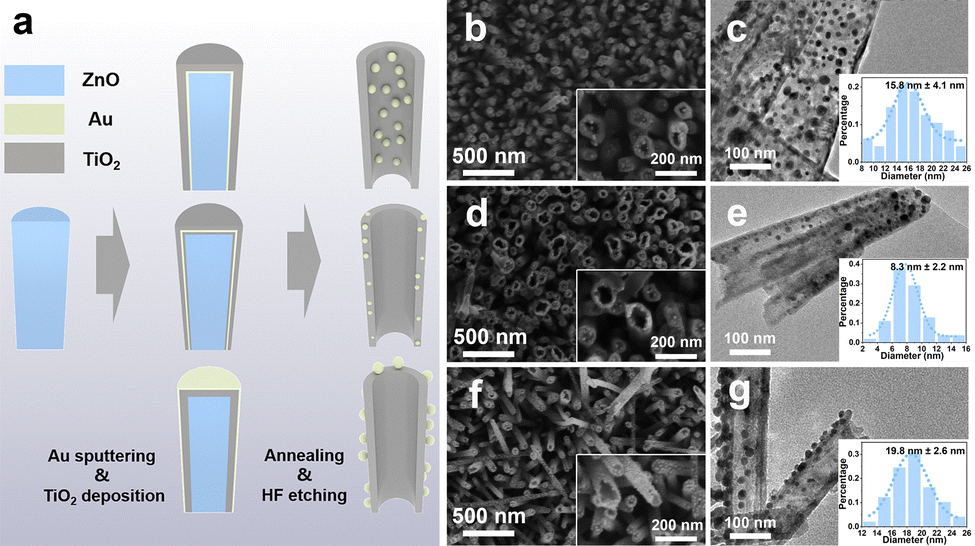 | ||
| Fig. 1 (a) Fabrication procedure for site-selective decoration of Au nanoparticles on TiO2 nanotubes by dewetting Au thin film. SEM images of Au–TiO2 (b), TiO2–Au–TiO2 (d), and TiO2–Au (f). TEM images of Au–TiO2 (c), TiO2–Au–TiO2 (e), and TiO2–Au (g); inset in each panel is the corresponding size distribution histogram of the loaded Au nanoparticles. | ||
The SEM images of the three samples intuitively depict the hollow structure of TiO2 nanotubes in the arrays. The Au nanoparticles are uniformly distributed inside the nanotubes for Au–TiO2 (Fig. 1b), embedded in the nanotube wall for TiO2–Au–TiO2 (Fig. 1d), and outside the nanotubes for TiO2–Au (Fig. 1f). Thus the site-selective localization of Au nanoparticles relative to the TiO2 shell is also clear. Although the thickness of the initial Au thin film was identical, there is a significant difference in the average size of Au nanoparticles for the three samples by analyzing the particle size based on TEM observations. The average sizes of the Au nanoparticles for Au–TiO2, TiO2–Au–TiO2, and TiO2–Au are 15.8 nm (Fig. 1c), 8.3 nm (Fig. 1e), and 19.8 nm (Fig. 1g), respectively.
We took Au–TiO2 as an example to further investigate the structural features of the Au-decorated TiO2 composite nanotubes. Fig. S1a (ESI†) shows a SEM image of the ZnO–Au–TiO2 core–shell nanowire array annealed at 500 °C for 1 h in air. The inhomogeneous contrast in the TEM image (Fig. S1b, ESI†) indicates the presence of a discontinuous Au particulate interlayer. The ALD-deposited TiO2 external layer is uniform with a thickness of 15 nm, agreeing with the value predetermined by the ALD cycles. Notably, the TiO2 shell is conformal to the substrate, which completely encapsulates the underlying ZnO–Au nanowire. Fig. 2a is a typical TEM image of the Au–TiO2 nanotubes that were converted from the annealed ZnO–Au–TiO2 nanowires by acidic etching. The nanotube wall slightly cracked due to the phase transition of TiO2 at 500 °C and the pressing of the Au nanoparticles subjected to an anisotropic pressure upon thermal expansion. In addition, Au nanoparticles of various sizes are densely distributed in the interior of the nanotube. In the high-resolution TEM image exhibited in Fig. 2b, the lattice spacing of 0.23 and 0.35 nm can be, respectively, attributed to the (111) plane of the Au nanoparticles and the (101) plane of the TiO2 nanotubes of the anatase phase. We can also observe the shrinkage of Au-enclosing TiO2 sections due to grain boundary diffusion during the sintering process. Fig. 2c shows the individual element mappings of the Au–TiO2 nanotubes. The elemental densities of Ti and O follow a decreasing trend along the edge to the interior, confirming its nanotube-like structure, while the dispersed nanoparticles only consist of Au. EDX elemental analysis in Fig. S2 (ESI†) reveals that the atomic ratio of Ti to Au is 2.83. The above microstructure characterizations verify the successful preparation of the Au–TiO2 nanotubes.
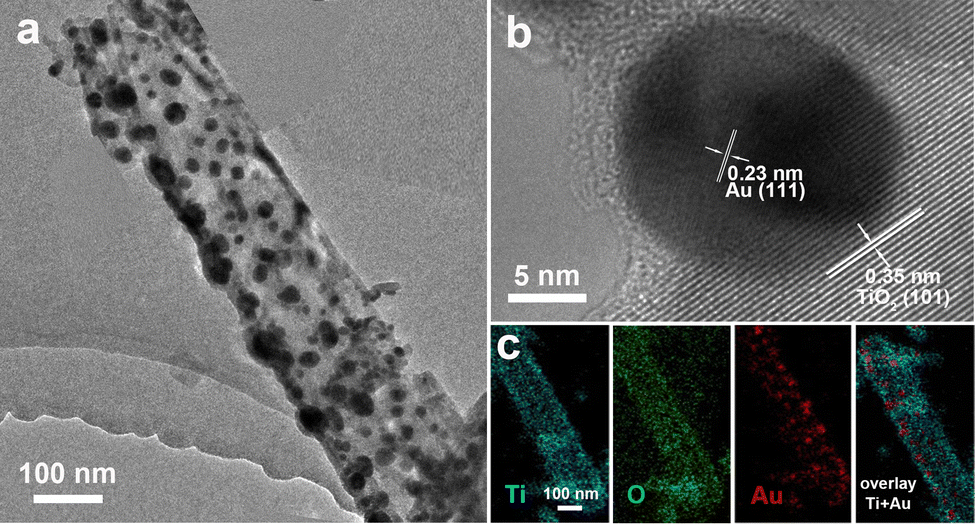 | ||
| Fig. 2 (a) TEM image of a selected Au–TiO2 nanotube. (b) HRTEM image of an area including the Au–TiO2 interface. (c) EDX elemental mappings of Ti, O, Au, and Ti + Au for the composite nanotube. | ||
Fig. 3a shows the XRD patterns of the annealed ZnO–Au–TiO2 sample and the different products of Au–TiO2, TiO2–Au–TiO2 and Au–TiO2. All the samples have a diffraction peak located at 25.5°, which corresponds to the (101) lattice plane of the anatase phase TiO2.30 This result reveals that the amorphous phase of the ALD-deposited TiO2 shells was transformed into anatase upon annealing at 500 °C. The distinct peaks of ZnO–Au–TiO2 at 31.8°, 34.4°, 35.2°, 47.5° and 62.8° can be assigned to (100), (002), (101), (102), and (103) lattice planes of wurtzite ZnO, which are absent from Au–TiO2, TiO2–Au–TiO2 and Au–TiO2, indicating the successful removal of the ZnO templates by acidic etching. However, the diffraction peaks of Au are not found in all the XRD patterns, which is probably caused by the small size, high dispersion and low quantity of the loaded Au nanoparticles.33
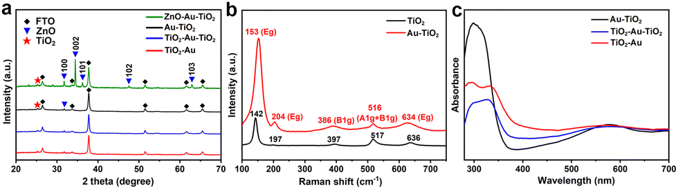 | ||
| Fig. 3 (a) XRD patterns of ZnO–Au–TiO2 annealed at 500 °C, Au–TiO2, TiO2–Au–TiO2 and TiO2–Au. (b) Raman spectra of single TiO2 and Au–TiO2 nanotubes. (c) UV-vis diffuse reflectance spectra of Au–TiO2, TiO2–Au–TiO2 and TiO2–Au. | ||
Fig. 3b exhibits the Raman spectra of the single TiO2 and Au–TiO2 nanotubes. The identical vibration modes of Eg (142 cm−1), Eg (197 cm−1), B1g (397 cm−1), A1g + B1g (517 cm−1), and Eg (636 cm−1) suggest that the TiO2 in the Au–TiO2 nanotubes is of tetragonal anatase structure. Its conventional cell consists of two primitive cells, each containing two TiO2 units, which is consistent with the results of the XRD patterns.34 The Raman scattering intensity of Au–TiO2 is significantly enhanced and slightly shifted compared to the single TiO2, which may be attributed to the plasmon resonance-assisted amplification of Raman scattering caused by the Au nanoparticles.35
The optical properties of the different Au-decorated TiO2 composite nanotubes were investigated by absorption spectroscopy. Fig. 3c shows the UV-vis diffuse reflectance spectra of Au–TiO2, TiO2–Au–TiO2, and TiO2–Au. As expected, the three samples show the characteristic absorption of TiO2 in the UV region, where the signal of Au–TiO2 is the strongest. In addition, a blue-shift of the absorption edge is observed for Au–TiO2 from 380 to 360 nm, different from those of TiO2–Au–TiO2 and TiO2–Au. The above phenomena demonstrate that the light absorption of the TiO2 nanotubes was affected by the size and site of the loaded Au nanoparticles, e.g. Au–TiO2 with Au nanoparticles decorated in the interior of TiO2 nanotubes, could reduce the shielding effect and ensure adequate UV light absorption by TiO2. Moreover, the enhanced light absorption in a wide visible region is observed for the three samples on account of the SPR absorption generated by the dewetted Au nanoparticles with various sizes.
For investigating the site-selective effect of the Au nanoparticles on the SERS performance of the Au-decorated TiO2 nanotubes, we employed R6G and MB as prototype probe molecules to explore the SERS behavior of Au–TiO2, TiO2–Au–TiO2 and TiO2–Au under 532 nm excitation. As shown in Fig. 4a and c, the three composite substrates provided enhanced Raman signals for both R6G and MB with a low concentration of 10−6 M, while the single TiO2 nanotube substrate was unresponsive (data not shown). The obtained Raman peaks agree well with the reported literature.36,37 Specifically, the characteristic peaks of R6G at 612, 774, 1186 and 1314 cm−1 can be individually assigned to C–C–C in-plane ring vibration, C–C–C out-of-plane bending vibration, C–H in-plane bending and C–O–C stretching motion. The other peaks observed in the positions of 1364, 1506 and 1652 cm−1 correspond to the stretching of the aromatic ring.36 In the case of MB, the weak intensity peaks around 669, 767 and 1071 cm−1 are derived from the out-of-plane and in-plane bending of C–H vibration. The peaks around 1394 cm−1 are caused by C–N symmetrical stretching vibration. The C–C ring stretching mode is attributed to the most intense peak located at around 1623 cm−1.37 Evidently the enhanced SERS signals depend on the decoration of Au nanoparticles on the TiO2 nanotube arrays. However, we also notice that the performance drastically varies with the loading sites of the dewetted Au nanoparticles, although the sputtered amount of Au is ideally the same for Au–TiO2, TiO2–Au–TiO2 and TiO2–Au. Fig. 4b and d summarize the spectral intensities of the three substrates by monitoring the characteristic peaks of R6G and MB, where Au–TiO2 presents a superior SERS activity to Au–TiO2–Au and TiO2–Au.
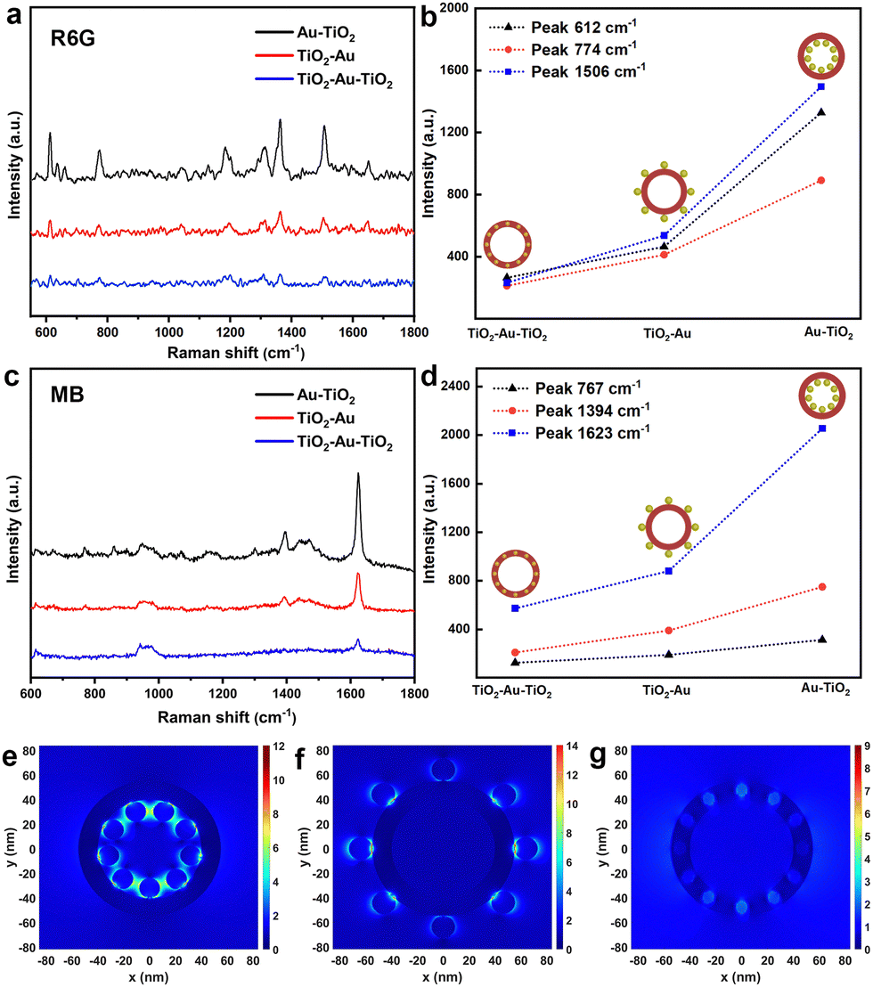 | ||
| Fig. 4 SERS spectra of R6G (a) and MB (c) with a concentration of 10−6 M on Au–TiO2, TiO2–Au–TiO2 and TiO2–Au under 532 nm excitation. SERS intensities of R6G at peaks of 612, 774, and 1506 cm−1 (b), and MB at peaks of 767, 1394, and 1623 cm−1 (d) for the three samples. (e)–(g) FDTD simulations of the optimized models of Au–TiO2, TiO2–Au, and TiO2–Au–TiO2 composite nanotubes. The EM-field enhancement was obtained by excitation at 532 nm. | ||
As verified by the microstructure analysis shown in Fig. 1, the site-selective decoration of the Au nanoparticles on the TiO2 nanotubes by dewetting the Au thin film of the same thickness resulted in a difference in the average size, which accordingly adjusted the interspaces between the Au nanoparticles distributed on the equal-area supports. It is known that Au atoms can diffuse to long distances on a heterogeneous surface at high temperatures.30,38 During the annealing process, the heat input first induced the disintegration of the Au thin film into isolated particles. Subsequently, the large particles grew and ripened by diffusion of Au atoms from the neighboring smaller particles according to the Gibbs–Thomson equations. For Au–TiO2, the spatial confinement between the internal ZnO nanowire and the TiO2 shell could retard the migration of Au atoms for formation of larger Au nanoparticles in the thermal diffusion process, whereas the Au nanoparticles formed in the TiO2 interlayer exhibited a much smaller size, suggesting the stronger binding force of the TiO2 bilayer constructed by ALD with the sandwiched Au thin film. With respect to TiO2–Au, the Au thin film was directly deposited on the external side of the ZnO/TiO2 core–shell nanowires, the dewetting process of which was merely influenced by the TiO2 support. As a result, the formed Au nanoparticles outside the nanotubes featured the largest size.
The 3D FDTD simulation was carried out to numerically estimate the EM field distribution in the three Au-decorated TiO2 nanotubes. The simulation models of Au nanoparticles at different locations of TiO2 nanotubes (Fig. S3, ESI†) were constructed by ideal geometric parameters based on the diverse particle size evolution from the identical Au thin film. Fig. 4e–g exhibit the EM field images of Au–TiO2, TiO2–Au and Au–TiO2–Au at an excitation wavelength of 532 nm. The dipole resonance intensity of the Au nanoparticles is known to be simultaneously correlated with their size and distribution, inducing a strong electric field, which favors the SERS signal of the adsorbed probe molecules. From the FDTD simulations, it can be observed that numerous EM hot spots are formed at the nanogaps of the Au nanoparticles in Au–TiO2via multiple plasmonic coupling (Fig. 4e). In contrast, fewer plasmonic coupling regions emerge between the Au nanoparticles in TiO2–Au, although the electric field intensity at the Au/TiO2 interface is greatly enhanced due to the larger size of the Au nanoparticles (Fig. 4f). In the case of TiO2–Au–TiO2 where Au nanoparticles are surrounded by TiO2, the change in the dielectric electric field environment causes Au–TiO2–Au to present the weakest EM field intensity (Fig. 4g).
Additionally, we simulated the EM field distributions in the three Au-decorated TiO2 nanotubes by taking the size distribution of the Au nanoparticles into account. The number of dewetted Au nanoparticles still stayed with the identical thickness of the initial Au thin film. Fig. S4 (ESI†) exhibits the EM field images of Au–TiO2, TiO2–Au and Au–TiO2–Au with a 20% size distribution of the Au nanoparticles. From the FDTD simulations, it is observed that more EM hot spots can form at the nanogaps of the Au nanoparticles in Au–TiO2 due to multiple plasmonic coupling, consistent with the results obtained from ideal geometric parameters based on the diverse particle size evolution. In order to evidence the effect of configuration on the formation of the hotspot region, we further conducted simulations under conditions of identical Au nanoparticle size and interspace to investigate the EM field associated with these three structural configurations. The results in Fig. S5 (ESI†) show that Au–TiO2 still exhibits the most significant EM field enhancement and the broadest hotspot region compared to TiO2–Au and TiO2–Au–TiO2 configurations. This observation suggests that the Au–TiO2 configuration offers distinct advantages for SERS performance. The multiple scattering of incident light within the nanotube cavity might contribute to amplifying the electric field intensity and expanding the coverage within the hotspot region. It can be concluded that the superior SERS performance of Au–TiO2 does not solely stem from the optimized spatial density of the Au nanoparticles but also from the unique Au–TiO2 configuration. Obviously, the probe molecules adsorbed on Au–TiO2 have a higher probability to be distributed in the electric field coupling region, thus achieving an effective enhancement of their Raman signals. Furthermore, Au–TiO2 could benefit from the capillary effect of TiO2 nanotubes, the cavities of which are capable of serving as molecular sinks to effectively enrich the probe molecules in the hotspot region distributed in the nanotube interior.
We further used Au–TiO2 as a substrate for Raman detection of the probe molecule R6G of different molecular concentrations. Fig. 5a shows the SERS spectra of R6G with a concentration ranging from 10−5 down to 10−9 M. The Raman peaks of R6G slowly decrease in intensity with decreasing concentration of R6G, and the signals are clearly observable at a concentration as low as 10−9 M, indicating a high sensitivity. The calculated analytical enhancement factor (AEF) of Au–TiO2 for R6G at 612 cm−1 is 6.64 × 10⁶ (ESI†). For investigating the reproducibility and stability of the SERS sensing that are important for the practicability of the substrate, Raman signals of R6G with a concentration of 10−5 M were collected by randomly taking 25 points on the Au–TiO2 substrate. As shown in Fig. 5b, the fluctuation of the peak intensity at 612 cm−1 is slight with a relative standard deviation (RSD) value of ∼0.12 (Fig. 5c), implying a uniform distribution of SERS hot spots on the entire substrate. In addition, after the as-prepared Au–TiO2 was stored in a wet environment for 10 days, the SERS spectrum of R6G obtained from the substrate is almost unchanged (Fig. S6, ESI†). The above results clearly demonstrate that the Au–TiO2 substrate possesses high stability, good uniformity and a low detection limit in SERS sensing, with potential in trace detection for molecules of interest.
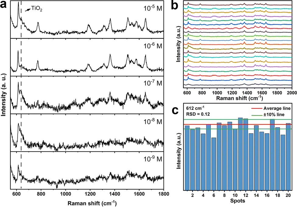 | ||
| Fig. 5 (a) SERS spectra of different concentrations of R6G molecule deposited on the Au–TiO2 substrate. (b) SERS spectra of R6G with a concentration of 10−5 M collected from 20 random sites on the Au–TiO2 substrate. (c) R6G signal intensities at 612 cm−1, presenting an RSD of 0.12. | ||
Considering the photocatalytic property of TiO2, we studied the self-cleaning ability of Au–TiO2, which is indispensable for a recyclable SERS substrate. The experiment of photocatalytic degradation of MB dye molecules in bulk solution was first applied under Xe lamp irradiation (100 mW cm−2) using Au–TiO2 (3 cm × 1 cm) as the photocatalyst. Fig. 6a shows the absorption spectra of MB (20 μM, 20 ml) during this process. As illustrated in Fig. 5b, the concentration of MB was reduced to 8% of the initial value within 120 min. The intimate contact between Au and TiO2 in Au–TiO2 is supposed to form a Schottky barrier, which could suppress the recombination of electrons and holes photogenerated in TiO2 and improve its photocatalytic activity for dye degradation.39 The cycling stability of Au–TiO2 as the photocatalyst was further investigated. The results summarized in Fig. 6b show that the degradation performance towards MB did not deteriorate after three degradation cycles operating under the same experimental conditions.
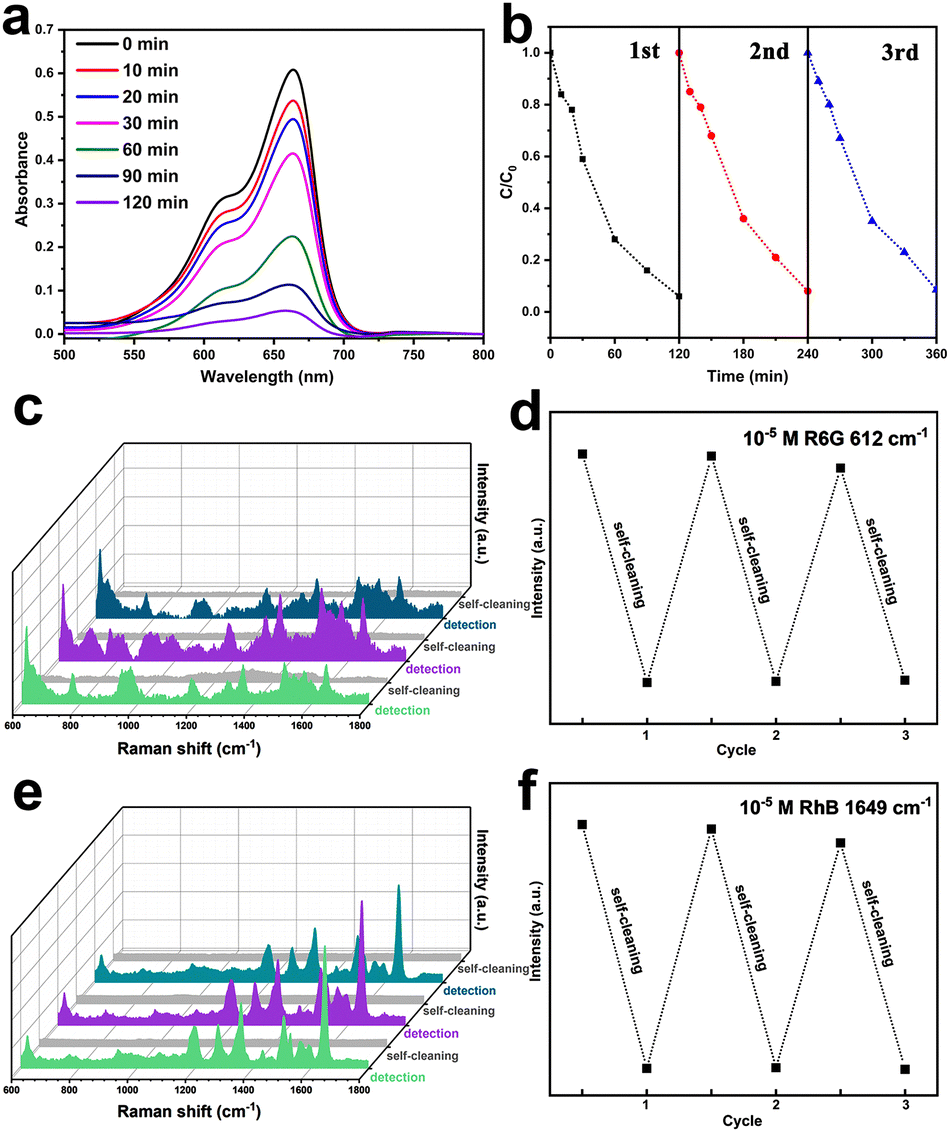 | ||
| Fig. 6 (a) UV-vis spectra of MB solution (20 μM, 20 ml) under Xe lamp irradiation for different times in the presence of Au–TiO2. (b) Cycle test results of photocatalytic degradation of MB. Reversible SERS behaviors of R6G (c) and (d) and RhB (e) and (f) by using the Au–TiO2 substrate during three cycles. | ||
On the basis that Au–TiO2 can effectively and continuously clean itself by photocatalytic degradation of the target molecules adsorbing on the surface, we examined its recyclable application as a self-cleaning SERS substrate. Fig. 6c shows the Raman spectra of R6G (10−5 M) measured on the Au–TiO2 SERS substrate via a procedure of detecting/cleaning in three consecutive cycles. Characteristic Raman peaks of R6G could be clearly identified by the initial SERS detection. After the used substrate was immersed in DI water and illuminated with a Xe lamp for 30 min, the Raman signals from R6G vanished, indicating a complete removal of the analyte by the cleaning treatment. As displayed in Fig. 6d, this reversible SERS behavior can sustain at least three cycles by tracking the intensity of the Raman peak at 612 cm−1. When RhB was used as the target probe molecule, we came to the same conclusion (Fig. 6e and f). Therefore, the Au–TiO2 substrate with efficient self-cleaning performance is expected to showcase its reversibility for a wide variety of organic analytes.
4. Conclusions
Au-decorated TiO2 nanotube arrays with different spatial distributions of Au nanoparticles have been successfully prepared via a top-down LbL deposition method using ZnO nanowires as structural templates. We demonstrate that regulating the thermal diffusion of the Au thin film in the confined ZnO/TiO2 interlayer favors an optimal distribution of the dewetted Au nanoparticles at the interstices with a small amount of Au consumption. By virtue of the size and interspace of the Au nanoparticles balancing each other, Au–TiO2 featuring Au nanoparticles dispersed on the inner walls of TiO2 nanotubes exhibited abundant localized EM field hot spots relative to those of TiO2–Au–TiO2 and TiO2–Au, which was supported by FDTD simulations. Accordingly, Au–TiO2 showed the best SERS activity, e.g. a detection limit of 10−9 M with an RSD of 0.12 for the R6G molecule. Meanwhile, the Au–TiO2 SERS substrate could achieve self-cleaning through photocatalytic degradation of the adsorbed organic analyte, which is required for repeated usage.Conflicts of interest
There are no conflicts to declare.Acknowledgements
This work is financially supported by the National Natural Science Foundation of China (21878157 and 22078156), and the Project of Priority Academic Program Development of Jiangsu Higher Education Institutions (PAPD).References
- N. Guarrotxena and G. C. Bazan, Adv. Mater., 2014, 26, 1941–1946 CrossRef CAS.
- X. Wang, S. C. Huang, T. X. Huang, H. S. Su, J. H. Zhong, Z. C. Zeng, M. H. Li and B. Ren, Chem. Soc. Rev., 2017, 46, 4020–4041 RSC.
- J. F. Li, Y. F. Huang, Y. Ding, Z. L. Yang, S. B. Li, X. S. Zhou, F. R. Fan, W. Zhang, Z. Y. Zhou, D. Y. Wu, B. Ren, Z. L. Wang and Z. Q. Tian, Nature, 2010, 464, 392–395 CrossRef CAS.
- Z. Q. Tian, J. S. Gao, X. Q. Li, B. Ren, Q. J. Huang, W. B. Cai, F. M. Liu and B. W. Mao, J. Raman Spectrosc., 1998, 29, 703–711 CrossRef CAS.
- M. Dendisová-Vyškovská, V. Prokopec, M. Člupek and P. Matějka, J. Raman Spectrosc., 2012, 43, 181–186 CrossRef.
- K. Kim and H. S. Lee, J. Phys. Chem. B, 2005, 109, 18929–18934 CrossRef CAS PubMed.
- D. Li, J. Q. Liu, H. B. Wang, C. J. Barrow and W. R. Yang, Chem. Commun., 2016, 52, 10968–10971 RSC.
- J. P. Lee, D. C. Chen, X. X. Li, S. Yoo, L. A. Bottomley, M. A. El-Sayed, S. Park and M. L. Liu, Nanoscale, 2013, 5, 11620–11624 RSC.
- S. Xie, D. Chen, C. Gu, T. Jiang, S. Zeng, Y. Y. Wang, Z. Ni, X. Shen and J. Zhou, ACS Appl. Mater. Interfaces, 2021, 13, 33345–33353 CrossRef CAS.
- S. Cong, Y. Yuan, Z. Chen, J. Hou, M. Yang, Y. Su, Y. Zhang, L. Li, Q. Li, F. Geng and Z. Zhao, Nat. Commun., 2015, 6, 7800 CrossRef CAS PubMed.
- K. Huang, C. Li, X. Zhang, X. Meng, L. Wang, W. Wang and Z. Li, Appl. Surf. Sci., 2020, 518, 146219 CrossRef CAS.
- G. Song, W. Gong, S. Cong and Z. Zhao, Angew. Chem., Int. Ed., 2021, 60, 5505–5511 CrossRef CAS PubMed.
- J. Lin, Y. Shang, X. Li, J. Yu, X. Wang and L. Guo, Adv. Mater., 2017, 29, 1604797 CrossRef.
- X. Tang, X. Fan, L. Yao, G. Li, M. Li, X. Zhao, Q. Hao and T. Qiu, J. Phys. Chem. Lett., 2022, 13, 7816–7823 CrossRef CAS.
- J. Huang, T. X. Zhou, W. S. Zhao, S. C. Cui, R. Guo, D. Li, N. R. Kadasala, D. L. Han, Y. H. Jiang, Y. Liu and H. L. Liu, J. Colloid Interface Sci., 2022, 628, 315–326 CrossRef CAS PubMed.
- J. Dong, Y. Wang, Q. Wang, Y. Cao, Q. Han, W. Gao, Y. Wang, J. Qi and M. Sun, Nanotechnology, 2022, 33, 135501 CrossRef.
- M. Sakir, E. Yilmaz and M. S. Onses, Microchem. J., 2020, 154, 104628 CrossRef CAS.
- P. Lv, C. Y. Zhao, W. J. Lee, S. P. Huo, S. H. Kwon, J. Fang and Y. Yang, Appl. Surf. Sci., 2019, 494, 508–518 CrossRef CAS.
- X. Li, G. Chen, L. Yang, Z. Jin and J. Liu, Adv. Funct. Mater., 2010, 20, 2815–2824 CrossRef CAS.
- Z. Dai, G. Wang, X. Xiao, W. Wu, W. Li, J. Ying, J. Zheng, F. Mei, J. Wang and C. Jiang, J. Phys. Chem. C, 2014, 118, 22711–22718 CrossRef CAS.
- J. Prakash, P. Kumar, R. A. Harris, C. Swart, J. H. Neethling, A. J. van Vuuren and H. C. Swart, Nanotechnology, 2016, 27, 355707 CrossRef.
- C. Xu, H. Geng, R. Bennett, D. A. Clayton and S. Pan, J. Phys. Chem. C, 2013, 117, 1849–1856 CrossRef CAS.
- J. Langer, D. J. de Aberasturi and J. Aizpurua, et al. , ACS Nano, 2022, 14, 28–117 CrossRef.
- S. Wang, J. Yao, Z. Ou, X. Wang, Y. Long, J. Zhang, Z. Fang, T. Wang, T. Ding and H. Xu, Nanoscale, 2022, 14, 4705–4711 RSC.
- J. Yu, G. A. Rancea and A. N. Khlobystov, J. Mater. Chem., 2009, 19, 8928–8935 RSC.
- C. V. Thompson, Annu. Rev. Mater. Res., 2012, 42, 339–434 CrossRef.
- K. Sugawara, M. Kawamura, Y. Abe and K. Sasaki, Microelectron. Eng., 2007, 84, 2476–2480 CrossRef CAS.
- Y. F. Wang, S. Ma, H. Yu, Y. Liu, J. Gao, L. Yang, M. Zhang, G. He and Z. Q. Sun, Nanotechnology, 2020, 32, 75708 CrossRef.
- Y. Cai, F. Y. Yuan, F. Li, H. H. Kang, D. X. Xue, S. P. Huo, F. J. Yu, J. Fang and Y. Yang, CrystEngComm, 2021, 23, 6551–6558 RSC.
- Y. Yang, R. B. Yang, H. J. Fan, R. Scholz, Z. Huang, A. Berger, Y. Qin, M. Knez and U. Gösele, Angew. Chem., Int. Ed., 2010, 49, 1442–1446 CrossRef CAS.
- Z. Y. Hu, H. J. Huang, F. Y. Yuan, Y. Cai, H. B. Shu, F. J. Yu, J. Fang and Y. Yang, J. Colloid Interface Sci., 2023, 644, 466–477 CrossRef CAS PubMed.
- S. Karim, M. E. Toimil-Molares, W. Ensinger, A. G. Balogh, T. W. Cornelius, E. U. Khan and R. Neumann, J. Phys. D: Appl. Phys., 2007, 40, 3767–3770 CrossRef CAS.
- W. F. Yan, V. Petkov, S. M. Mahurin, S. H. Overbury and S. Dai, Catal. Commun., 2005, 6, 404–408 CrossRef CAS.
- C. Engelbrekt, K. T. Crampton, D. A. Fishman, M. Law and V. A. Apkarian, ACS Nano, 2020, 14, 5061–5074 CrossRef CAS.
- O. L. Stroyuk, V. M. Dzhagan, A. V. Kozytskiy, A. Y. Breslavskiy, S. Y. Kuchmiy, A. Villabona and D. Zahn, Mater. Sci. Semicond. Process., 2015, 37, 3–8 CrossRef CAS.
- X. Z. Wang, Z. Wang, M. Zhang, X. S. Jiang, Y. F. Wang, J. G. Lv, G. He and Z. Q. Sun, J. Alloys Compd., 2017, 725, 1166–1174 CrossRef CAS.
- H. Chen, Z. Yang and S. Lee, Langmuir, 2016, 32, 10184–10188 CrossRef CAS PubMed.
- E. Florez, F. Vines, J. A. Rodriguez and F. Illas, J. Chem. Phys., 2009, 130, 244706 CrossRef.
- Q. Deng, X. W. Duan, D. H. L. Ng, H. B. Tang, Y. Yang, M. G. Kong, Z. K. Wu, W. P. Cai and G. Z. Wang, ACS Appl. Mater. Interfaces, 2012, 4, 6030–6037 CrossRef CAS.
Footnote |
| † Electronic supplementary information (ESI) available. See DOI: https://doi.org/10.1039/d3tc03702a |
| This journal is © The Royal Society of Chemistry 2024 |