
Enhanced nanogenerator by embedding lead-free double perovskite Cs2AgBiBr6 in polymer matrix for hybrid energy harvesting†
Mengrou
Wang
 a,
Xin
Wang
a,
Yubing
Xu
a,
Shunjie
Chai
a,
Zhiwei
Zhao
a,
Qing
Li
a,
Jun
Wu
a,
Jing
Chen
a,
Zhuoya
Zhu
a,
Byung Seong
Bae
b,
Razika
Tala-Ighil
c,
Jianming
Zhou
d,
Ying
Zhu
e and
Wei
Lei
*a
a,
Xin
Wang
a,
Yubing
Xu
a,
Shunjie
Chai
a,
Zhiwei
Zhao
a,
Qing
Li
a,
Jun
Wu
a,
Jing
Chen
a,
Zhuoya
Zhu
a,
Byung Seong
Bae
b,
Razika
Tala-Ighil
c,
Jianming
Zhou
d,
Ying
Zhu
e and
Wei
Lei
*a
aSchool of Electronic Science and Engineering, Joint International Research Laboratory of Information Display and Visualization, Southeast University, Nanjing 210000, China. E-mail: lw@seu.edu.cn
bDepartment of Electronics & Display Engineering Hoseo University, Hoseo Ro 79, Asan city, Chungnam 31499, Republic of Korea
cDepartment of Physics, URMPE Unit, UMBB University, 35000 Boumerdes, Algeria
dE-xray Electronic Co. Ltd, Suzhou 215131, China
eE-spectrum Optoelectronic Co. Ltd., Suzhou 215111, China
First published on 27th November 2023
Abstract
Mechanical energy harvesters fabricated with halide perovskites display excellent electrical output because of their prominent permittivity. An all-inorganic lead-free double perovskite, Cs2AgBiBr6 (CABB), with competitive performance, excellent environmental stability and non-toxicity can break the confines of practical unavailability. CABB microcrystals, which are effective nucleating agents and dielectric fillers, are embedded into a polyvinylidene-fluoride (PVDF)-matrix as efficient electron-acceptors to induce electro-active PVDF β-phase formation and enhance the composite dielectric constant, which contributes to notable hybrid electric outputs. CABB–PVDF hybrid nanogenerators with the optimal CABB concentration of 20 wt% possess triboelectric and piezoelectric effects, with a nanogenerator with a 1.2 cm × 1.2 cm effective contact area and 70 μm film thickness exhibiting a unique response with an open-circuit voltage of 126 V and a short-current density of 4.67 mA m−2 under a 0.5 Hz mechanical frequency and 4 cm s−1 motion speed. An identical device achieves the highest output power density of 0.39 W m−2 at 8 Hz and 0.64 m s−1, which could light up at least 86 commercial LEDs using a 1 μF capacitor and power small electronic devices such as a timer using 22 μF. The corresponding force sensing is achieved with a different distribution of external forces using a 10 wt% CABB–PVDF composite film. This functional composite maintains its stability and charge retention capacity for effective application in various environmental conditions.
1. Introduction
Energy harvesting from mechanical vibrations1,2 or biomechanical movements3 using eco-friendly energy-harvesting technologies has inspired considerable research enthusiasm in convenient environmental energy collection and electrical energy conversion.4,5 Nanogenerators (NGs), including triboelectric6 (TE) NGs and piezoelectric7 (PE) NGs, are potentially convenient and efficient energy harvesting schemes that have extensive applications as sustainable power sources for small-scale portable electronic devices8 due to their advantages of simple implementation mechanism,9 convenient manufacturing process,10 diverse material selections,11 and abundant structural designs.12 To effectively convert distributed low-frequency mechanical energy13 into usable electricity, TENGs usually separate opposite polarity charges originating from the contact of different substances through the TE effect14 based on the coupling of contact electrification and electrostatic induction, while the electricity in PENGs originates from the mechanical deformation15 of the PE material between two electrodes. Although multitudinous explorations have been conducted before, output power density improvement is still an urgent challenge16 that limits the popularization of NGs. Embedding fillers in polymers17 to synthesize composite polymer films (CPFs) is utilized to increase the dielectric constant (ε) and surface charge density of materials, which could result in TENG performance improvement. Polydimethylsiloxane (PDMS) and polyvinylidene fluoride (PVDF) are highly common and useful polymer supporting materials for latent TE and PE properties in NG-type devices. K. Ghosh18et al. incorporated micropatterns on a PDMS/Ti3C2TxMXene surface utilizing 3D printing technology and acquired a negative TE material, which achieved an open-circuit voltage (Voc) of 146 V and a short-circuit current (Isc) at 32 μA when a 2.8 N, 10 Hz external force was applied. Yu's group19 prepared a hybrid nanogenerator (HENG) based on a PVDF/PDMS-barium titanate nanowires (BTO)–carbon nanotube (CNT) composite nanofiber through an electrospinning process, whose maximum output power density was 223.7 mW m−2 with a 100 MΩ load, and this continuous power source could supply electricity to small electronic devices.Having excellent flexibility and PE properties,20 PVDF-based compositions are usually used to produce high-performance NGs with high β-phase content, because this all-trans conformation (TTTT) crystalline phase has the largest polarization with the best electroactive properties. Many of the various inorganic additives, such as reduced graphene oxide (rGO),21 molybdenum disulfide (MoS2),22 and so on, exhibit complexity and cost-intensive processing that confine their fabrication and growth; hence, finding new functional materials that act as promotive additives,23 such as the noteworthy halide perovskite-like materials, has strong potential to enhance NG performance. Halide perovskite-like materials are already the most promising star in areas such as photovoltaics,24 photo-detection,25 light-emitting diodes,26etc., because of their remarkable optoelectronic properties. These properties originate from the semiconducting and ionic properties of perovskites, which serve as effective nucleating agents and could facilitate the conversion of amorphous- or nonpolar-phase PVDF into the polar β-crystalline phase. In some recent studies, CsPbI2Br-decorated PVDF nanofibers27 possessed the most desirable morphology and functionality with a Voc of 8.3 V and ISC of 1.91 μA. Considering the PE effect of PVDF, using the above functional materials to establish HENGs28,29 could be regarded as a progressive scheme to achieve an efficient energy conversion mode. F. Jiang30et al. used Cs3Bi2Br9 as a functional filler to prepare a poly(vinylidene fluoride-co-hexafluoropropylene) (PVDF-HFP)-based composition; the resulting HENG achieved an enhanced Voc and short-current density (Jsc) of 400 V and 1.63 μA cm−2. Additionally, stable and environmentally friendly lead-free double perovskite materials with the structure A2BI+BII3+X6 (ref. 31–33) also have bright application prospects because their comparable performance makes them competitive substitutes with traditional lead-halide perovskite; the bismuth-based double perovskite Cs2AgBiBr6 (CABB) can be regarded as the most representative of these materials.
Various methods have been proposed for composite film preparation, including electrospinning,34 one-step co-precipitation,23 and blade coating technology,35etc. Rather than the above tedious processes, the CABB–PVDF based composites were prepared by spin-coating with additional drop-casting in this work to form a HENG device using CABB as the effective filler material. This flexible composite film incorporates CABB as an efficient electron acceptor into the PVDF matrix as well, inducing the nucleation of β-phase PVDF. According to our study, the CABB–PVDF composite film with a CABB concentration of 20 wt% (20 wt% CABB@PVDF film) had improved electron-trapping ability and effective polarization of PVDF; its suitable concentration and band structure also provide the possibility to reduce the charge loss and enhance electrical performance. With an effective contact area (S) of 1.2 cm × 1.2 cm and a film thickness of 70 μm, the 20 wt% CABB@PVDF film could achieve a Voc of 126 V and a Jsc of 4.67 mA m−2 with 0.5 Hz and 4 cm s−1 external motivation; this device could access the highest output power density of 0.39 W m−2 at 8 Hz and 0.64 m s−1, with a corresponding internal resistance of 500 MΩ. By charging different capacitors, the above device could light up at least 86 commercial LEDs using a 1 μF capacitor and power some small electronic devices such as a timer at 22 μF as well. Moreover, the PE effect related to the PVDF phase was also verified by FTIR characterization, with the corresponding force sensing also being achieved using a different distribution of external forces and 10 wt% CABB@PVDF film. Although the optimal concentrations for PE and TE are inconsistent, the optimum HENG output exhibits the same effect with TE corresponding to its optimal dielectric constant. Finally, via the encapsulation and protection of the PVDF polymer, the stability and charge retention capacities of CABB have also been greatly strengthened, which is crucial for its application in environmental conditions.
2. Results and discussion
The simple one-step compound synthesis method for the preparation of the lead-free double perovskite CABB-polyvinylidene fluoride (PVDF) composites is schematically illustrated in Fig. 1(a). CABB crystals are formed in advance through a controlled cooling crystallization method, as previous research reported.33,36 The moisture-stable and flexible CABB@PVDF films are then synthesized by embedding various contents of the as-prepared CABB microcrystal (MC) powder in PVDF; the annealing process supports the growth of the MCs. The change in the color of the surface of the composite films from translucent to orange indicates the dispersion of the CABB MCs into the PVDF matrix. The cross-sectional structure of the 20 wt% CABB@PVDF film is presented in detail in Fig. 1(b). Fig. 1(b1) shows the schematic structure of the composite film, in which the cubic CABB MCs, which are circled in red in the cross-section structure (Fig. 1(b2)), are randomly scattered in the PVDF film. As shown in Fig. S1a (ESI†), the average thickness of the prepared composite films was almost 31.48 μm, where the mean CABB MC particle size is 22.77 μm at corresponding concentration, as shown in Fig. S2d4 (ESI†). Fig. 1(c) and Fig. S2a (ESI†) depict the surface morphologies of CABB@PVDF films with different CABB contents, which were obtained using the spin-coating with additional drop-casting and spin-coating-only method, respectively. Due to the effects of the additional drop-casting, the film thickness increases and ensures a tight connection between the films on the substrates, as they separate easily if only dropping is used. An obviously remarkable phenomenon is observed, namely, the MC particle size increases with the enhancement of the CABB content. As shown in Fig. 1(c8), the size changes from 0.71 μm or 8.93 μm at 5 wt% to 2.12 μm or 39.86 μm at 64 wt%; the relevant particle sizes in Fig. 1(c8) were obtained by Gaussian fitting in Fig. S2c and d (ESI†) simultaneously. In the concentration range from 0 wt% to 20 wt%, CABB MCs only form on the surface or interior of the composite films rather than throughout the cross-section,37 where the larger grain size contributes to an effective S with inconspicuous surface roughness changes; also, the sufficient CABB serves as efficient electron trapping acceptors to preserve more negative charges and enhance the TE output.30 However, when the content exceeds 20 wt%, excessive CABB causes the MCs to stretch across the entire membrane, which results in agglomeration on the surface of the CABB@PVDF films, which impedes the interaction between CABB and PVDF, causes incomplete contact between two TE surfaces, and eventually reduces the output properties. The elemental (C, F, Cs, Ag, Bi and Br) mapping images of 20 wt% CABB@PVDF film in Fig. 1(d) and Fig. S2b (ESI†) also reveal a uniform dispersion of CABB in the PVDF polymer at the 50 μm scale; this homogeneous matrix formation illustrates the regular position of the CABB microstructures within the PVDF network. The SEM-energy dispersive X-ray spectroscopy (EDS) spectra in Fig. 1(d1) and Fig. S2b2 (ESI†) confirm the presence of the elements C, F, Cs, Ag, Bi and Br in the composite films and equally verify the CABB structure of Cs![[thin space (1/6-em)]](https://www.rsc.org/images/entities/char_2009.gif) :Ag:Bi:Br = 2:1:1:6, yielding an estimated chemical composition of A2BI+BII3+X6 type. Some basic optical properties are then illustrated in Fig. 1(e)–(g), which present the ultraviolet-visible (UV-Vis) absorption spectrum, photoluminescence (PL) spectrum and time-resolved PL (TRPL) information, respectively. As shown in the inset figure in Fig. 1(e), with increasing CABB content in the composite films, their surface color becomes deep orange, with the absorption intensity growing strongly. Compared with those of pure CABB in Fig. 1(e), the absorption intensities of the composite films remain at a lower level for lower relative CABB content, but the absorption cutoff is the same as that of CABB at about 524 nm, while the pure PVDF is almost transparent in the visible range. The PL intensities of the CABB@PVDF films in Fig. 1(f) generally have a positive correlation with the CABB content, and are lower than that of pure CABB. Due to the intensified light scattering and refraction loss38,39 of the CABB@PVDF composites, the fluorescence efficiency decrease in the CABB MCs leads to intensities lower than that of pure CABB. Additionally, the PL peak position of the composite films moves to 636 nm, which represents a blue shift of 42 nm compared to that of CABB at 678 nm, and was ascribed to the passivation and high interaction between CABB and PVDF chains.40 Compared with the negligible light response of pure PVDF, the absorption and PL intensities of the composite films were all clearly enhanced. Fig. 1(g) presents the TRPL transformation regulation (changing rules of the curves) fitting using a two-exponential-decay model, which indicates that the CABB@PVDF film may have increased trap states and act as additional radiative relaxation channels, leading to the decrease in radiative decay rates and charge-carrier lifetime compared with pure CABB.41,42 The weighted-average PL decay time (τavg) of the 20 wt% CABB@PVDF film is 1.7 μs, while those of pure PVDF and pure CABB are 869 ns and 3.8 μs, respectively. Further, the carrier lifetime of the composite films increases with the enhancement of the CABB content; the inset figure in Fig. 1(g) shows that a higher CABB doping amount could eliminate the nonradiative recombination pathway effectively by passivating defects.
:Ag:Bi:Br = 2:1:1:6, yielding an estimated chemical composition of A2BI+BII3+X6 type. Some basic optical properties are then illustrated in Fig. 1(e)–(g), which present the ultraviolet-visible (UV-Vis) absorption spectrum, photoluminescence (PL) spectrum and time-resolved PL (TRPL) information, respectively. As shown in the inset figure in Fig. 1(e), with increasing CABB content in the composite films, their surface color becomes deep orange, with the absorption intensity growing strongly. Compared with those of pure CABB in Fig. 1(e), the absorption intensities of the composite films remain at a lower level for lower relative CABB content, but the absorption cutoff is the same as that of CABB at about 524 nm, while the pure PVDF is almost transparent in the visible range. The PL intensities of the CABB@PVDF films in Fig. 1(f) generally have a positive correlation with the CABB content, and are lower than that of pure CABB. Due to the intensified light scattering and refraction loss38,39 of the CABB@PVDF composites, the fluorescence efficiency decrease in the CABB MCs leads to intensities lower than that of pure CABB. Additionally, the PL peak position of the composite films moves to 636 nm, which represents a blue shift of 42 nm compared to that of CABB at 678 nm, and was ascribed to the passivation and high interaction between CABB and PVDF chains.40 Compared with the negligible light response of pure PVDF, the absorption and PL intensities of the composite films were all clearly enhanced. Fig. 1(g) presents the TRPL transformation regulation (changing rules of the curves) fitting using a two-exponential-decay model, which indicates that the CABB@PVDF film may have increased trap states and act as additional radiative relaxation channels, leading to the decrease in radiative decay rates and charge-carrier lifetime compared with pure CABB.41,42 The weighted-average PL decay time (τavg) of the 20 wt% CABB@PVDF film is 1.7 μs, while those of pure PVDF and pure CABB are 869 ns and 3.8 μs, respectively. Further, the carrier lifetime of the composite films increases with the enhancement of the CABB content; the inset figure in Fig. 1(g) shows that a higher CABB doping amount could eliminate the nonradiative recombination pathway effectively by passivating defects.
 | ||
| Fig. 1 (a) Fabrication process of flexible CABB@PVDF film, including synthesis procedure, annealing time and film structure schematic. (b) Structure of 20 wt% CABB@PVDF film. (b1) Schematic structure. (b2) Cross-section view. (c) Surface morphology of CABB@PVDF films with different CABB contents obtained by the spin-coating and additional drop-casting method. (c1)–(c7) Surface morphology for CABB contents of 0–64 wt%. (c8) Grain size change regulation with CABB content increase. (d) EDS spectrum and elemental (C, F, Cs, Ag, Bi and Br) mapping images of 20 wt% CABB@PVDF film obtained by the spin-coating and additional drop-casting method. (e) UV-Vis, (f) PL spectra, and (g) TRPL of CABB@PVDF films with CABB contents of 0–64 wt%. | ||
X-ray diffraction (XRD) patterns were used to analyze the PVDF phase of the CABB@PVDF film, as depicted in Fig. 2(a). The inset picture in Fig. 2(a1) presents a schematic of the CABB structure; all composite films have CABB diffraction peaks, as the red marks emphasize. Additionally, pure PVDF possesses a strong α diffraction peak, which represents an electrically inactive nonpolar phase, at 17.7°, 18.3° and 19.9°, corresponding to the (100), (020) and (021) reflections.43 Through the addition of CABB MCs, the PVDF composite films generate the dominant electroactive β-phase at 20.6° belonging to the (110)/(200) reflection of the orthorhombic β-PVDF phase. The detailed PVDF phase diffraction positions of the various composites are as shown in Fig. 2(a2). Regrettably, XRD analysis cannot quantify β-phase content, but the Fourier transform infrared (FTIR) spectra in Fig. 2(b) can calculate it27 in detail. The vibrational bands at 765, 795, and 976 cm−1 are ascribed to the PVDF α-phase, while those at 840 and 1275 cm−1 indicate the electroactive β-phase, and that at 1234 cm−1 suggests the semi-electroactive γ-phase. The addition of CABB MCs usually induces electroactive β-phase formation due to the interaction of CABB with PVDF polymer chains, because the negatively charged ions that originate from the ionic nature of CABB can interact with the positively charged CH2 group. The PVDF β-phase contents are obtained as follows:44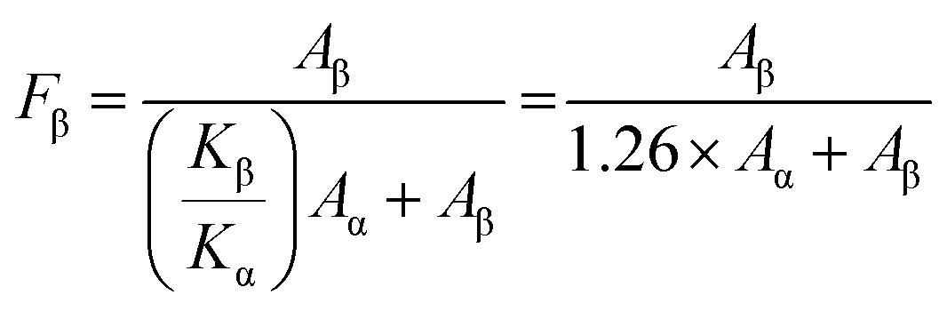 , where Aα and Aβ are the absorbance values at 765 and 840 cm−1, respectively, while Kα and Kβ are two constants with values of 6.1 × 10⁴ and 7.7 × 104 cm2 mol−1, respectively. The PVDF β-phase contents in Fig. 2(b2) indicate that the optimum doping amount that generates the most effective polarization is 10 wt% CABB, which gives 73.4% β-phase content; the uniformly distributed CABB contributes to abundant β-phase induction. Lower CABB contents are insufficient to fully polarize PVDF, but the agglomeration of CABB MCs on the polymer surface at ultra-high content would expose the ionic semiconductor CABB to the environment, accelerating surface charge dissipation and thus impeding β-phase generation and degrading electrical performance, which is consistent with the XRD conclusions. The above effects are also analyzed in the schematic diagram in Fig. 2(c). The suitable dispersion concentration of 10 wt% causes CABB to be encased in PVDF well, and the polymer could have a protective function in reducing perovskite charge dissipation. This ratio also accelerates β-phase nucleation, with self-polarization forming a built-in electric field at the interface of CABB and PVDF, avoiding the excessive occurrence of depolarization. HENGs usually exhibit compound PE and TE effects. The PE effects and corresponding simulation are presented in Fig. 2(d) and (e). When an external force is applied to dielectrics in a specific direction, polarization inside the material will occur and form numerous dipoles, gathering positive and negative charges on the opposite surfaces simultaneously. To balance the electrode potential, the induced electrostatic charges accumulated at the top and bottom surfaces of the CABB@PVDF film cause negative charges to flow through external circuit. When the compression force is withdrawn, the negative charges flow back, which maintains the electrostatic neutral state of the film. Hence, external periodic mechanical signals can induce the PE alternating current (AC). The COMSOL results in Fig. 2(e) theoretically describe the surface potential distribution of the above film under external forces. Similarly, the PE properties Voc and ISC for different CABB contents are presented in Fig. 2(f) and (g). As the CABB content is varied, the peak PE signals occur at 10 wt%, where the highest Voc is 6.4 V and the ISC is 64.2 nA with an effective S of 2 cm × 2 cm and a 30 N mechanical force, confirming the XRD and FTIR results.
 | ||
| Fig. 2 (a) XRD patterns, (b1) FTIR spectra, and (b2) PVDF β-phase contents of CABB@PVDF films with different CABB contents. (c) Schematic diagram of PVDF phase change and CABB contributions. (d) Whole “press-release” cycle of the PENGs an external pressure is applied. Three motion states are no force, compressed and released. (e) PE potential distribution simulated using COMSOL. The forces exerted on PENG are 0 N and ±0.1 MPa (±10 N). The physical size of the PENG is 2 cm × 2 cm. Voc and Jsc (f) measurements and (g) peak of composite film PENGs with different CABB contents. | ||
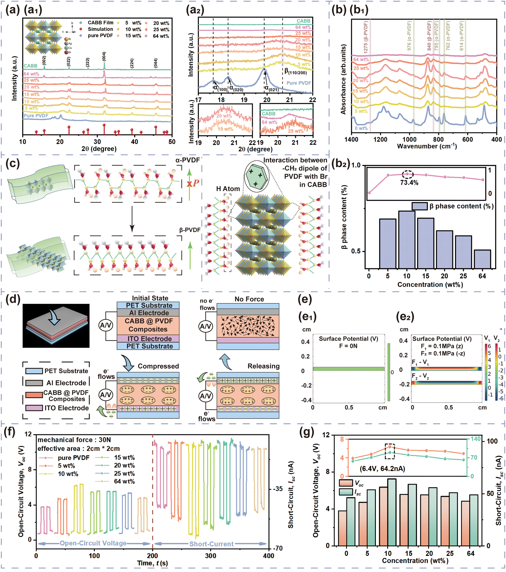
The relative dielectric constant (εr) and dielectric loss (loss tangent, tanδ) of the CABB@PVDF film in Fig. 3(a) were measured using a parallel plate capacitor model through scanning the frequency from 10 Hz to 10 MHz in the dark. The εr value, which is a meaningful parameter for characterizing the output performance of a HENG, increases as the CABB doping content increases within the range of 0–20 wt%, especially in the low-frequency region, where the highest εr of the composite film with 20 wt% is 25.12 at 1 kHz, and the corresponding tanδ is 0.23. The improved dielectric properties of the composite films derive from the mixture of PVDF with high-εr CABB and the large dipole–dipole interactions or interfacial polarization37,43 at the interfaces between two heterogeneous materials of conductive particles in composite films with higher CABB content. The adjacent particle distance becomes shorter as the CABB content increases, and then forms micro-capacitor structures between dielectric adjacent particles, which leads to abundant polarization charges being stored in an electric field.45,46 As the CABB content continues to increase, εr diminishes due to the weak insulating nature of the composite films, which easily allows electrical breakdown in the sample.47 Unusually, excessive CABB causes surface agglomeration and thus a higher εr, but the higher tanδ restrains the output level as well. Fig. 3(b) and (c) also depict the HENG effects. During a “press–release” working period, no voltage or current flow exists in the initial electrostatic equilibrium state. When periodic mechanical signals are initiated, the CABB@PVDF and PET surface begins to become polarized and leads to charge transfer at separation, and charge recombination then occurs when the surfaces contact lightly. In the triboelectrification process, the CABB@PVDF films are negatively charged because they are electronegative, causing charges to flow from the PET electrodes to the composite film electrodes. As the force continues to cause closer contact, the PE effect subsequently occurs as shown in Fig. 2(d) and (e), creating small charge transfer. After removing the external forces, both TE and PE charges are generated, and a higher reverse current occurs. The COMSOL simulation in Fig. 3(c) also presents the electric potential distribution in the contact and separated states. Similarly, the hybrid output parameters Voc and Jsc for different CABB contents are shown in Fig. 3(d) and (e), which show that the HENG with an effective S of 1.2 cm × 1.2 cm possesses the highest Voc of 126 V and Jsc of 4.67 mA m−2 with a f of 0.5 Hz and a motion speed (v) of 4 cm s−1 when the CABB content is 20 wt%.
 | ||
| Fig. 3 (a and a1) Measured εr, (a2) tanδ, and (a3) εr and tanδ at 1 KHz of composite films with different CABB contents. (b) Whole “press–release” cycle of HENG illustrated by motion displacement d. The five motion states are fully released, pressing started, fully contacting, compressed, and release started. (c) TE effects on potential distribution simulated using COMSOL. The gaps d are 1 μm and 4 mm. The physical size of the HENG is 1.2 cm × 1.2 cm. Voc and Jsc (d) measurements and (e) peaks for the composite film HENGs with different CABB contents. | ||
Based on Fig. 3(d) and (e), 20 wt% CABB was considered to be the best doping ratio; hence, qualitative analysis of the surface elements on the above film and pure CABB was implemented through X-ray photoelectron spectroscopy (XPS) characterization. The XPS scan in Fig. 4(a) verifies the existence of the elements C, F, Cs, Ag, Bi, and Br in the 20 wt% CABB@PVDF film (referred to as the composite film in this paragraph) and of the elements C, Cs, Ag, Bi, and Br in pure CABB based on the distinctive elemental peaks; the top curves are pure CABB, and the bottom curves are the composite film. For the composite film, the C 1s peak exhibits three components at 284.8 eV, 286.5 eV, and 291.0 eV corresponding to the C–C, H–C–H, and F–C–F bonds of PVDF, respectively. The F 1s peak at 688.2 eV demonstrates the existence of organic fluorine. Pure CABB has only a C1 peak at 284.8 eV, which comes from the environment. The Cs 3d spectrum indicating the presence of Cs+ features two peaks of Cs 3d3/2 at 739 eV and Cs 3d5/2 at 725 eV in the composite film, which move 1.3 eV toward the lower-energy direction compared with the Cs 3d3/2 peak at 737.7 eV and Cs 3d5/2 peak at 723.7 eV for pure CABB. Similarly, the peaks of Ag 3d3/2 at 374.3 eV and Ag 3d5/2 at 368.3 eV in the composite film have a 1 eV shift compared with the peaks of Ag 3d3/2 at 373.3 eV and Ag 3d5/2 at 367.3 eV for pure CABB. Additionally, the Bi3+ valence state peaks of Bi 4f5/2 at 164.5 eV and Bi 4f7/2 at 159.16 eV in the composite film are also 0.7 eV higher in energy than those of Bi 4f5/2 at 163.8 eV and Bi 4F7/2 at 158.46 eV for pure CABB. The Br 3d peaks of Br 3d3/2 at 69.6 eV and Br 3d5/2 at 68.6 eV in the composite film also present a peak movement of 0.9 eV compared with Br 3d3/2 at 68.7 eV and Br 3d5/2 at 67.7 eV in pure CABB, and correspond to the existence of Br−. The binding energy values shifted positively (toward higher binding energy on the spectrum) compared with those of pure CABB due to the interfacial interactions between the –CF2/–CH2 dipoles of the PVDF polymer and CABB.43,48 The electrostatic interactions between PVDF and CABB contribute to the self-orientation of the polymer chains, which lead to electroactive β-phase formation. Kelvin probe force microscopy (KPFM) characterization was also used to determine the surface potential changes before and after the formation of composite, where probe makes tiny displacement vibrations along the surface to capture surface potential, as shown in Fig. 4(b). The surface roughness and potential of pure PVDF are 0.41 μm and −710.9 mV, as presented in Fig. 4(c), while they are 1.8 μm and −969.2 mV for the composite film, as Fig. 4(d) indicates. Due to the presence of dipoles, the trapped electrons inside CABB cause positive charges to accumulate on its surface, thus leading to the potential of the PVDF region of composite film being inferior to that of pure PVDF. Abrupt surface potential changes in the composite film are clearly found in the vicinity of the CABB periphery, which is due to the accumulation of opposite polarity charges at the CABB and PVDF interfaces resulting in the existence of macroscopic dipoles, whereas the pure PVDF surface potential remains stable due to its smooth surface morphology. Furthermore, the more undulating surfaces and enhanced surface potential of the composite film compared with pure PVDF give rise to electroactive behavior, which could lead to synergic effects and increase the TE charging ability of the device.49 The polarization intensity of ferroelectrics changes along with the electric field, as shown in the polarization versus electric field (P–E) loop in Fig. 4(e), which represents the polarization response of the composite film under the action of an external electric field. The coercive field (Ec), residual polarization intensity (Pr), and spontaneous polarization intensity (Ps) of the composite film were: Ec = 30.71 kV cm−1, Pr = 0.018 μC cm−2, and Ps = 0.0615 μC cm−2, where Pr = 0.29 Ps. The smooth and wide P–E loop with diagonal ends originates from the defects of CABB–PVDF and complex stresses. In addition, CABB50 matches the energy levels of PVDF51 (HOMO: highest occupied molecular orbital, LUMO: lowest unoccupied molecular orbital) well compared to other perovskites (MAPbBr3, CsPbBr3, Cs3Bi2Br9) or inorganic oxides (ZnO, TiO2), as shown in Fig. 4(f). Due to the intrinsic defects of CABB, trap states distributed between the conduction and valence bands can accommodate more electrons, leading to improved promoting HENG output performance for the embedded CABB MCs. Fig. 4(g) shows the electron transfer and trapping mechanism of the HENG during the whole motion period. When contact occurs, the electrons transfer from the PET (PET energy level52) surface to the PVDF LUMO level and then are rapidly captured by CABB trap states, considering that electrons tend towards transition to lower energy levels. When separation occurs, the composite films release electrons through the peripheral circuit to maintain potential balance, which leads to pulse current formation. This explanation verifies the macroscopic working mechanism in Fig. 2(d) and 3(b).
 | ||
| Fig. 4 (a) XPS spectrum of CABB and 20 wt% CABB@PVDF film. (b) KPFM of (c) PVDF and (d) 20 wt% CABB@PVDF film. (e) P–E loop of 20 wt% CABB@PVDF film. (f) Comparison of energy levels with those of other materials. (g) Illustration of the energy levels of CABB–PVDF HENG and the corresponding electron transfer and trapping process. | ||
Fig. 5 explores some factors influencing the HENG output characteristics of the 20 wt% CABB@PVDF film. The film thickness data in Fig. 5(a) and (b) demonstrates that a thickness of 1 μm usually results in the best Voc and Jsc of 157 V and 5.08 mA m−2, respectively, when applying an f of 0.5 Hz and a v of 4 cm s−1 with an S of 1.2 cm × 1.2 cm. When the thickness is lower than 1 μm, the output response increases as the thickness improves, because it is highly related to number of accumulated charges. A thicker film generates and gathers sufficient tribo-charges to enhance electric output. However, the response gradually weakens when the thickness exceeds 1 μm, because excessive thickness enlarges the distance between the electrode and surface, limiting the electrostatic induction effect.53Fig. 5(c) and (d) present the effect of S on the response; Voc and ISC exhibit a monotonically increasing trend, but Jsc decreases as the effective S increases. When the f is 0.5 Hz and the v is 4 cm s−1 with a thickness of 70 μm, the Voc, ISC, and Jsc values change from 90.8 V, 0.4 μA, and 6.2 mA m−2 to 210 V, 1.8 μA, and 1.5 mA m−2 as the size changes from 0.8 cm × 0.8 cm to 3.5 cm × 3.5 cm. The enlarged S could accommodate more surface charges, but an excessively increased S would reduce contact effectivity.54 The f value associated with v also affects the outputs, as shown in Fig. 5(e) and (f). Generally speaking, due to the excellent charge trapping capacity of the composite film, higher v leads to faster electron transfer, hence providing a higher Voc, Jsc and output power, correspondingly. Under 4 cm initial gap between two relative surfaces, Voc and Jsc increase rapidly when f changes from 0.125 to 8 Hz, with the corresponding increased dipole moment changing rate resulting in a decrease of escaped charges, thus leading to charge accumulation on the two surfaces at higher impact frequency.55 The peak-to-peak Voc and Jsc increase from 33.8 V and 2.1 mA m−2 to 209.9 V and 11.0 mA m−2, respectively, when f increases from 0.125 to 8 Hz. However, as f continues to rise, Voc and Jsc decline because of restricted charge transfer due to transient contact.56 Further, the f values associated with the motion distance in Fig. 5(g) and (h) also indicate that Voc and Jsc show continuous growth as the distance is reduced or f is increased at a constant v of 4 cm s−1. The Voc and Jsc increase from 76 V and 2.45 mA m−2 to 132 V and 4.81 mA m−2, respectively, as f changes from 0.125 to 8 Hz.
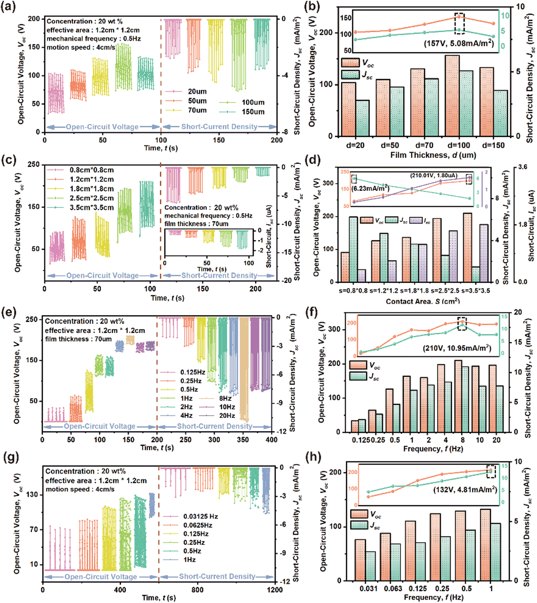 | ||
| Fig. 5 (a), (c), (e), and (g) Voc and Jsc measurement results, and (b), (d), (f), and (h) Voc and Jsc peaks of 20 wt% CABB@PVDF film HENGs under different test conditions. Influence of (a), (b) film thickness and (c), (d) S. Influence of (e), (f) v and (g), (h) motion distance associated frequency. | ||
The long-time stability test in Fig. 6(a) confirms the strong robustness of the device under 1000 s of continuous motion at a speed of 4 cm s−1 and frequency of 0.5 Hz; Voc fluctuates within 136.3 V to 124.9 V, and the Jsc loss is not significant. Through the rectifier transformation depicted in Fig. 6(b), the dispersed low-frequency mechanical energy becomes reusable energy to produce a direct current (DC), which could power small portable electronic devices or charge a lithium-ion battery to store electrical energy. Numerous factors in Fig. 6(c) and (d) indicate that both capacitance and v are key to influencing the charging speed. Lower capacitance and higher v positively influence the Voc and Jsc. Fig. 6(c) shows that to charge to 0.2 V using different capacitors but the same f of 4 Hz (or v of 0.32 m s−1), a circuit with a 0.1 μF capacitance only requires 0.95 s, but a 1000 μF circuit requires 100 s. Additionally, after 100 s of charging, the voltage of a 3.3 μF capacitor increases to 4.2 V, but the voltage only reaches 0.2 V for a 1000 μF capacitor. As shown in Fig. 6(d), the motion f or v have analogous effects in terms of charge capability. For 0.1 μF, the HENG only requires 1.1 s to charge to 1.88 V at 8 Hz or 0.64 m s−1, while it needs 100 s at 0.125 Hz. An f of 8 Hz achieves the fastest charging speed, presenting a positive correlation with the frequency magnitude when lower than 8 Hz. When the value reaches 20 Hz, the charging rate slows down for Voc and appears to decrease, as shown in Fig. 5(e) and (f). Owing to the extremely high number of accumulated charges, the strong electric field generation causes air breakdown,57 which limits the retainable surface charge and reduces the output performance accordingly. The insets in Fig. 6(c) and (d) present the charging behavior in one motion cycle; the capacitor begins to charge at contact, but remains stable or discharges slowly when separated.58Fig. 6(e) then evaluates the load voltage, load current density, and output power density at 8 Hz. The maximum output power density of the 20 wt% CABB@PVDF film HENG is 0.39 W m−2 with a 500 MΩ load. When f is kept constant, the highest output power density can be acquired when the external resistance matches the internal resistance according to the maximum power transfer theory. The load voltage rises constantly and the load current decreases as the resistance is raised from 10 KΩ to 2 GΩ, and the optimal output power density is produced at 500 MΩ because of equilibration with the internal resistance. Fig. 6(f) and (g) present the influence of relative humidity (RH) and temperature (T) on stability. As the RH rises in Fig. 6(f), the Voc presents an obvious downward trend, which is reversible when the RH decreases to ambient RH due to the excellent hydrophobicity of PVDF. Higher RH usually results in a layer of water on the composite surface, which thus impedes the production of charges by contact electrification. As shown in Fig. 6(g), an appropriate T could dissipate surface vapor, which contributes to higher Voc. However, excessive T will lead to charge escape due to the thermal excitation of surface charges, reducing Voc as well. Due to the outstanding reversibility and adaptability of CABB, the Voc could be restored by cycling RH and T. Fig. 6(h) demonstrates that a 20 wt% CABB@PVDF film with an effective area of 1.2 cm × 1.2 cm could light up more than 86 LEDs under 0.1 μF and 8 Hz (or 0.64 m s−1) test conditions; this device can release the stored electricity to light LEDs and only requires 30 s to charge from 0 V to 210 V. Further, as depicted in Fig. 6(i), it requires almost 640 s to charge from 0 V to 2.5 V at 22 μF with an f of 8 Hz or v of 0.64 m s−1; the stored electricity could then be utilized to power a timer. Comparisons of the properties of the perovskite-based or PVDF-composition-based TENG structures and their output features are listed in Table S1 (ESI†).
 | ||
| Fig. 6 (a) Stability test of the Voc and Jsc of the PET/ITO/20 wt% CABB@PVDF//PET/Al HENG with an S of 1.2 cm × 1.2 cm over 1000 s. (b) Rectifier application in energy conversion systems. Charging curves of the above HENG at (c) various capacitances but the same f of 4 Hz, or (d) various f values but the same capacitance of 0.1 μF. (e) Load voltage, load current density and output power density of the above HENG under various external load resistances. Influence of (f) RH and (g) T on Voc (above) and Jsc (below). (h) 84 commercial yellow LEDs lighted by the above HENG using a 0.1 μF capacitor with an f of 8 Hz (or v of 0.64 m s−1). (i) Timer powered by the above HENG using a 22 μF capacitor and an f of 8 Hz (or v of 0.64 m s−1). | ||
Finally, some PE effects are also examined in detail in Fig. 7. Fig. 7(a) presents the measured piezo-response under different bending angles to examine its mechanical flexibility and outputs. As the bending angle increases, the corresponding stress, Voc and ISC are enhanced as well. PE output can be obtained by bending (0.1 MPa) the composite layer, as shown in Fig. 7(b); the Voc and ISC responses are 1.33V and 20.1nA, respectively. Thus, this versatile and robust composite layer has the potential to be applied to various devices other than TENGs. Fig. 7(c)–(e) presents the detection of several human physiological motions using a polymer-based PENG attached directly on a human as a wearable sensor based on its flexibility. During the detection of body joint movements, such as finger-, elbow- and knee-bending, the device remains stable and does not generate any electrical output when the joints are fully straightened, but the Voc of the sensor gradually rises as the joint bends. Hence, the above device could be integrated with a self-powered smart electronics system as a sensor. Additionally, a 3 × 5 pressure sensor array using a 10 wt% CABB@PVDF composite film was realized in practical application, in which the size of each sensor was 0.8 cm × 0.8 cm and each sensor was considered to be one pixel, as shown in Fig. 7(f1). Fig. 7(f2) presents a theoretical current distribution when the force impacted at the corresponding pixels, while the actual instantaneous spatially distributed pressure was recorded as current and is presented in Fig. 7(f3); as shown, instantaneous current generation only occurred where a force existed. An identical experiment and the corresponding result using the PVDF-only device is shown in Fig. S4 (ESI†).
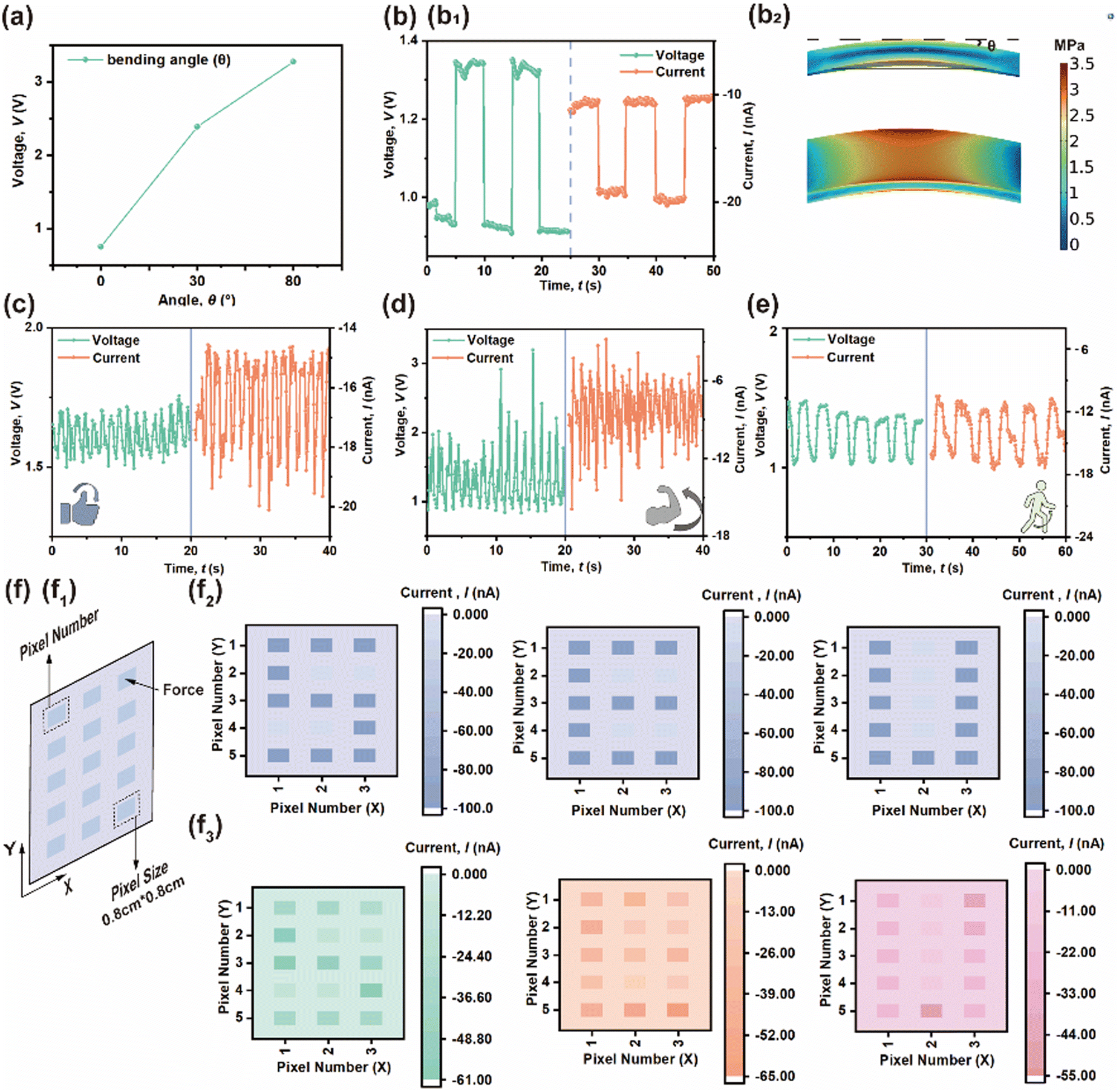 | ||
| Fig. 7 (a) PENG Voc at different bending angles. (b1) Voc and ISC response and (b2) corresponding force distribution under 0.1 MPa bending. Voc and ISC in the (c) finger-, (d) elbow-, and (e) knee-bending state. (f) 3 × 5 pressure sensor array based on 10 wt% CABB@PVDF film. (f1) Pressure sensor array schematic; size of each sensor size is 0.8 cm × 0.8 cm. (f2) Theoretical and (f3) actual current distribution when force impacted at the relevant pixels. | ||
3. Experimental section
3.1 Materials and reagents
All reagents and solvents are commercially available and were used as received. Hydrobromic acid in water (HBr, 48 wt%), cesium bromide (CsBr, 99.9%) and silver bromide (AgBr, 99.9%) were obtained from Aladin. Bismuth bromide (BiBr3, 98%), anhydrous isopropanol (IPA, 99.5%) and polyvinylidene fluoride (PVDF, Mw ∼ 45000) were purchased from Macklin. Anhydrous ethanol (AE, 99.7%), acetone (99.5%) and N,N-dimethylformamide (DMF, 99.9%) were acquired from Sinopharm Chemical Reagent Co., Ltd. All chemicals were used without any further purification. ITO PET substrates were purchased from South China Science & Technology Company Limited. PET commercial films with a thickness of 50 μm were obtained from Shanghai Huadong Compound Insulating Filter Cloth & Mesh Factory.
3.2 Preparation of CABB crystals
The CABB crystals were obtained as prepared by researchers previously.33,36 Firstly, CABB crystals were obtained according to a procedure previously reported by Slavney et al.36 2.13 g (10 mmol) CsBr, 2.25 g (5 mmol) BiBr3 and 0.94 g (5 mmol) AgBr were dissolved in 60 ml HBr under stirring at 125 °C for 2 h until the solution clarified. After the temperature was decreased to ambient temperature in an ice bath, red shattered crystals were achieved. The finished products were cleaned with IPA and dried in a vacuum oven at 60 °C.3.3 Preparation of various CABB–PVDF composite films with different CABB concentrations
ITO PETs with a size of 2 cm × 2 cm × 1.1 mm were first cleaned using an ultrasonic process in detergent, deionized water, acetone and IPA for 15 min each. After 5 min of ozone-UV treatment on the ITO surface, the ITO PETs were preheated at 60 °C on an IKA-RET hotplate before use.To fabricate composite polymer films, an initial PVDF polymer solution was prepared by dissolving 0.1 g PVDF powder in 1 ml DMF under constant stirring at 70 °C for 24 h. The CABB–PVDF composite precursors were then prepared by mixing 1 ml PVDF solution with various weight percentages (0 wt%, 5 wt%, 10 wt%, 15 wt%, 20 wt%, 25 wt%, and 64 wt%) of as-prepared CABB powder under continuous stirring at 75 °C for 2 h on a hotplate. Limited by the solubility of CABB in DMF, the highest CABB weight percentage was 64%.
The composition then was spin-coated onto the already prepared substrates (ITO-coated PET substrates) at 500 rpm for 8 s and 1000 rpm for 10 s, respectively, followed by drying on a hotplate at 110 °C for 20 min. These newly prepared substrates were cut to 1.5 cm × 1.5 cm because of the uneven edges, fully covered with the corresponding composition solution using the drop-casting method, and then reannealed under the above conditions to form a dense and uniform film. The final composite films possessed an effective contact area of 1.2 cm × 1.2 cm due to the existing uneven edges. Other composite films with different dimensions were prepared using the same method but with different substrate sizes. Composite films with the same concentration but different thicknesses were prepared using different volumes of solution and measured using high-precision vernier calipers.
3.4 Fabrication of CABB–PVDF composite film HENGs
Further, these composite films were used to construct HENGs having a structure of PET/ITO/CABB–PVDF composition//PET/Al. The HENG was assembled using a typical vertical contact-separation mode, where the CABB–PVDF composition film was the negative TE layer and a commercial PET film (50 μm in thickness) was the positive one. The PET films had the same size as the composite films. The ITO PETs supported the CABB–PVDF composite film and served as the bottom electrode, while conductive aluminium (Al) adhesive tape with a size of 1.2 mm × 1.2 mm × 60 μm was the top electrode and was connected to the PET film. Lastly, parts of both the top and bottom electrodes of the nanogenerators (1.2 cm × 1.2 cm) were connected to copper wires using conductive silver paste. These two layers were fixed on the mover and stator of a linear motor, respectively. Other CABB–PVDF HENGs with different areas or thickness had the same configuration, except that different composite films were used. Studies on the mixing concentration, film thickness, motion frequency corresponding to motion speed or relative distance, output response, and influence factors of properties all used the HENG with an active area of 1.2 cm × 1.2 cm. Studies on area used composite films and PET films with other sizes. Ambient humidity was maintained at 28–32%, and ambient temperature was kept at 15 °C. The studies on temperature and humidity used the control variable method. The composite film thickness in the above studies was 70 μm except in the film-thickness-related research. For the PENG devices, the Al electrode was directly prepared on the surface of the composite films and grounded the surface during the test. The PENG size was 2 cm × 2 cm, while each array element was 0.8 cm × 0.8 cm.3.5 Characterizations and measurements
Scanning electron microscope (SEM) images and SEM-energy dispersive X-ray spectroscopy (EDS) spectra were obtained using a Quanta 200 FEI (United States). Absorption spectra were achieved through UV-VIS spectroscopy using a Lab Tech Bluestar (USA). Photoluminescence (PL) spectra and carrier lifetime (τ) were measured using a fluorescence spectrometer (FS5, Techcomp). X-ray diffraction (XRD) patterns were obtained using a Rigaku SmartLab SE (Japan). Fourier transform infrared (FTIR) spectra were measured using a Thermo Scientific Nicolet iS20 (USA). The relative dielectric constant and dielectric loss (loss tangent) were measured using an impedance analyzer (Agilent 4294A). Atomic force microscopy (AFM) and Kelvin probe force microscopy (KPFM) images were taken using a Bruker Dimension Icon (German). X-ray photoelectron spectroscopy (XPS) tests were achieved using a Thermo Scientific ESCALAB 250Xi (USA). The polarization–electric field (P–E) hysteresis curves were measured under room ambient conditions using a PK-FERRO20B (USA) operated in virtual ground mode. All electrical performance measurements were accessed using a linear motor (RXP45). Open-circuit voltage (Voc) and short-circuit current density (Jsc) curves were measured using a Keithley 2400 through Voltmeter mode or Current meter mode. Rectifiers, various capacitors, resistors, and commercial yellow LEDs were obtained from Risym (Shen Zhen, China).4. Conclusions
CABB–PVDF-based composites were fabricated simply in this work to form a HENG device using CABB as an effective filler material. In terms of the PE effect, the improved electro-active β-phase content of 73.4% verified by FTIR for the 10 wt% CABB@PVDF film prompts dipole generation and could achieve a different distribution of external forces. Additionally, the hybrid output mainly originates from the optimal dielectric constant with 20 wt% CABB due to its stronger TE effect. The composition with 20 wt% CABB content could improve electron-trapping ability and polarize PVDF effectively, which further reduced charge loss and enhanced electrical performance due to the band structure matching. With an effective S of 1.2 cm × 1.2 cm and film thickness of 70 μm, the 20 wt% CABB@PVDF film could achieve a Voc of 126 V and Jsc of 4.67 mA m−2 with a f of 0.5 Hz and a v of 4 cm s−1. The above device achieved the highest output power density of 0.39 W m−2 with a f of 8 Hz and v of 0.64 m s−1, and matching internal resistance of 500 MΩ as well. Additionally, at least 86 commercial LEDs can be lit up using a 1 μF capacitor, while small electronic devices such as a timer can be powered at 22 μF. This composite film also possesses effective applications under environmental conditions due to its stability and charge retention capacity.Author contributions
W. Lei and M. Wang supervised the project throughout the whole process of all experiments. M. Wang and X. Wang grew crystals. M. Wang and S. Chai realized COMSOL simulations. M. Wang and Y. Xu synthesized composite films and did electrical experiments. M. Wang, Z. Zhao, Q. Li, J. Wu, J. Chen, Z. Zhu, B. Bae, R. Tala-Ighil, J. Zhou, Y. Zhu, and W. Lei analyzed results and wrote the manuscript. All authors made comments on the manuscript.Conflicts of interest
The authors declare that they have no known competing financial interests or personal relationships that could have appeared to influence the work reported in this paper.Acknowledgements
This work is financially supported by National Key Research and Development Program of China (2022YFE0139100, 2021YFE0105900), National Natural Science Foundation Project of China (62175028, 51879042, 61674029), National Natural Science Foundation Project for Young Researcher (12005038), Program 111_2.0 in China (BP0719013), Leading Technology of Jiangsu Basic Research Plan (BK20192003), International cooperative research project of Jiangsu province (BZ2022008).References
- X. Li, C. Zhang, Y. Gao, Z. Zhao, Y. Hu, O. Yang, L. Liu, L. Zhou, J. Wang and Z. L. Wang, Energy Environ. Sci., 2022, 15, 1334–1345 RSC.
- D. Wang, D. Zhang, M. Tang, H. Zhang, F. Chen, T. Wang, Z. Li and P. Zhao, Chem. Eng. J., 2022, 446, 136914 CrossRef CAS.
- Z. Xu, D. Li, K. Wang, Y. Liu, J. Wang, Z. Qiu, C. Wu, J. Lin, T. Guo and F. Li, Appl. Energy, 2022, 312, 118739 CrossRef.
- C. Zhi, S. Shi, S. Zhang, Y. Si, J. Yang, S. Meng, B. Fei and J. Hu, Nano-Micro Lett., 2023, 15, 60 CrossRef PubMed.
- M. V. Paranjape, S. A. Graham, P. Manchi, A. Kurakula and J. S. Yu, Small, 2023, 19, e2300535 CrossRef.
- H. Varghese, H. M. A. Hakkeem, K. Chauhan, E. Thouti, S. Pillai and A. Chandran, Nano Energy, 2022, 98, 107339 CrossRef CAS.
- C. Chen, S. Zhao, C. Pan, Y. Zi, F. Wang, C. Yang and Z. L. Wang, Nat. Commun., 2022, 13, 1391 CrossRef CAS PubMed.
- Y. Qin, J. Mo, Y. Liu, S. Zhang, J. Wang, Q. Fu, S. Wang and S. Nie, Adv. Funct. Mater., 2022, 32, 2201846 CrossRef CAS.
- X.-S. Zhang, M.-D. Han, B. Meng and H.-X. Zhang, Nano Energy, 2015, 11, 304–322 CrossRef CAS.
- G. Du, J. Wang, Y. Liu, J. Yuan, T. Liu, C. Cai, B. Luo, S. Zhu, Z. Wei, S. Wang and S. Nie, Adv. Sci., 2023, 10, 2206243 CrossRef CAS.
- Q. Duan, W. Peng, J. He, Z. Zhang, Z. Wu, Y. Zhang, S. Wang and S. Nie, Small Methods, 2023, 7, 2201251 CrossRef CAS PubMed.
- W. G. Kim, D. W. Kim, I. W. Tcho, J. K. Kim, M. S. Kim and Y. K. Choi, ACS Nano, 2021, 15, 258–287 CrossRef CAS.
- H. Zhao, M. Xu, M. Shu, J. An, W. Ding, X. Liu, S. Wang, C. Zhao, H. Yu, H. Wang, C. Wang, X. Fu, X. Pan, G. Xie and Z. L. Wang, Nat. Commun., 2022, 13, 3325 CrossRef.
- H. Zou, L. Guo, H. Xue, Y. Zhang, X. Shen, X. Liu, P. Wang, X. He, G. Dai, P. Jiang, H. Zheng, B. Zhang, C. Xu and Z. L. Wang, Nat. Commun., 2020, 11, 2093 CrossRef CAS.
- Y. Dobashi, D. Yao, Y. Petel, T. N. Nguyen, M. S. Sarwar, Y. Thabet, C. L. W. Ng, E. S. Glitz, G. T. M. Nguyen, C. Plesse, F. Vidal, C. A. Michal and J. D. W. Madden, Science, 2022, 376, 502–507 CrossRef CAS PubMed.
- C. Wu, A. C. Wang, W. Ding, H. Guo and Z. L. Wang, Adv. Energy Mater., 2019, 9, 1802906 CrossRef.
- K. Eom, Y. E. Shin, J. K. Kim, S. H. Joo, K. Kim, S. K. Kwak, H. Ko, J. Jin and S. J. Kang, Nano Lett., 2020, 20, 6651–6659 CrossRef CAS.
- K. Ghosh, C. Iffelsberger, M. Konečný, J. Vyskočil, J. Michalička and M. Pumera, Adv. Energy Mater., 2023, 13, 2203476 CrossRef CAS.
- B. Zhao, L. Lei, Y. Zhu, Z. Cheng, Y. Liu, S. Wang, M. Liu, T. Yu, W. Yang and Y. Li, Chem. Eng. J., 2023, 461, 142086 CrossRef CAS.
- L. Shi, H. Jin, S. Dong, S. Huang, H. Kuang, H. Xu, J. Chen, W. Xuan, S. Zhang, S. Li, X. Wang and J. Luo, Nano Energy, 2021, 80, 105599 CrossRef CAS.
- S. K. Karan, R. Bera, S. Paria, A. K. Das, S. Maiti, A. Maitra and B. B. Khatua, Adv. Energy Mater., 2016, 6, 1601016 CrossRef.
- M. Kim, D. Park, M. M. Alam, S. Lee, P. Park and J. Nah, ACS Nano, 2019, 13, 4640–4646 CrossRef CAS.
- L. Chen, M. He, L. Li, S. Yuan, A. Chen, M. Chen, Y. Wang, L. Sun, L. Wei, T. Zhang, Q. Li and Q. Zhang, Chem. Eng. J., 2022, 450, 138279 CrossRef CAS.
- Z. Zhang, Q. Sun, Y. Lu, F. Lu, X. Mu, S. H. Wei and M. Sui, Nat. Commun., 2022, 13, 3397 CrossRef CAS.
- X. Zhang, Y. Yao, L. Liang, X. Niu, J. Wu and J. Luo, Angew. Chem., Int. Ed., 2022, 61, e202205939 CrossRef CAS.
- B. Liu, J. Li, G. Wang, F. Ye, H. Yan, M. Zhang, S.-C. Dong, L. Lu, P. Huang, T. He, P. Xu, H.-S. Kwok and G. Li, Sci. Adv., 2022, 8, eabq0138 CrossRef CAS.
- S. Wu, F. Zabihi, R. Y. Yeap, M. R. Y. Darestani, A. Bahi, Z. Wan, S. Yang, P. Servati and F. K. Ko, ACS Nano, 2023, 17, 1022–1035 CrossRef CAS.
- Y. P. Lim, J. S. C. Koay, J. Zhao, S. Huang, B. T. Goh, K. C. Aw, B. Chen, C. Y. Haw and W. C. Gan, Adv. Funct. Mater., 2022, 32, 2206750 CrossRef CAS.
- S. Hajra, A. M. Padhan, M. Sahu, P. Alagarsamy, K. Lee and H. J. Kim, Nano Energy, 2021, 89, 106316 CrossRef CAS.
- F. Jiang, X. Zhou, J. Lv, J. Chen, J. Chen, H. Kongcharoen, Y. Zhang and P. S. Lee, Adv. Mater., 2022, 34, 2200042 CrossRef CAS.
- H. Yin, Y. Xian, Y. Zhang, W. Chen, X. Wen, N. U. Rahman, Y. Long, B. Jia, J. Fan and W. Li, Adv. Funct. Mater., 2020, 30, 2002225 CrossRef CAS.
- L. Wang, W. Zheng, F. Vitale, X. Zhang, X. Li, Y. Ji, Z. Liu, O. Ghaebi, C. T. Plass, R. Domes, T. Frosch, G. Soavi, E. Wendler, Y. Zhang and C. Ronning, Adv. Funct. Mater., 2022, 32, 2111338 CrossRef CAS.
- W. Pan, H. Wu, J. Luo, Z. Deng, C. Ge, C. Chen, X. Jiang, W.-J. Yin, G. Niu, L. Zhu, L. Yin, Y. Zhou, Q. Xie, X. Ke, M. Sui and J. Tang, Nat. Photonics, 2017, 11, 726–732 CrossRef CAS.
- Y. Xue, T. Yang, Y. Zheng, E. Wang, H. Wang, L. Zhu, Z. Du, X. Hou and K.-C. Chou, J. Mater. Chem. A, 2022, 10, 21893–21904 RSC.
- S. Shen, Y. Zhao, R. Cao, H. Wu, W. Zhang, Y. Zhu, K. Ren and C. Pan, Nano Energy, 2023, 110, 108347 CrossRef CAS.
- A. H. Slavney, T. Hu, A. M. Lindenberg and H. I. Karunadasa, J. Am. Chem. Soc., 2016, 138, 2138–2141 CrossRef CAS.
- V. Jella, S. Ippili, J.-H. Eom, J. Choi and S.-G. Yoon, Nano Energy, 2018, 53, 46–56 CrossRef CAS.
- H. Luo, Y. Yang, Y. Wang and J. Hou, Compos. Commun., 2021, 27, 100818 CrossRef.
- H. Luo, J. Hu, Y. Dou, Y. Yang and J. Hou, Compos. Commun., 2020, 22, 100516 CrossRef.
- Z. Anajafi, M. Naseri and G. Neri, Sens. Actuators, B, 2020, 304, 127252 CrossRef CAS.
- J. J. Yoo, G. Seo, M. R. Chua, T. G. Park, Y. Lu, F. Rotermund, Y. K. Kim, C. S. Moon, N. J. Jeon, J. P. Correa-Baena, V. Bulovic, S. S. Shin, M. G. Bawendi and J. Seo, Nature, 2021, 590, 587–593 CrossRef CAS.
- W. Wu, C. Zhao, M. Hu, A. Pan, W. Xiong and Y. Chen, Nanoscale, 2023, 15, 5705–5711 RSC.
- S. Ippili, V. Jella, J. Kim, S. Hong, H.-S. Kim and S.-G. Yoon, Nano Energy, 2022, 103, 107781 CrossRef CAS.
- S. D. Mahapatra, P. C. Mohapatra, A. I. Aria, G. Christie, Y. K. Mishra, S. Hofmann and V. K. Thakur, Adv. Sci., 2021, 8, 2100864 CrossRef CAS.
- X. Liu, X.-R. Sun, C. Luo, H.-Z. Ma, H. Yu, Y. Shao, M.-B. Yang and B. Yin, J. Mater. Chem. C, 2022, 10, 265–273 RSC.
- G. Jian, M. Liu, C. Yan, F. Wu, B. Song, K.-S. Moon and C.-P. Wong, Nano Energy, 2019, 58, 419–426 CrossRef CAS.
- S. Ippili, V. Jella, A. M. Thomas, C. Yoon, J.-S. Jung and S.-G. Yoon, J. Mater. Chem. A, 2021, 9, 15993–16005 RSC.
- Z. Zhao, J. Wu, Y.-Z. Zheng, N. Li, X. Li and X. Tao, ACS Catal., 2019, 9, 8144–8152 CrossRef CAS.
- Y. H. Lee, D. H. Kim, Y. Kim, I. Shabbir, M. Li, K. H. Yoo and T. W. Kim, Nano Energy, 2022, 102, 107676 CrossRef CAS.
- Z. Zhang, Q. Sun, Y. Lu, F. Lu, X. Mu, S. H. Wei and M. Sui, Nat. Commun., 2022, 13, 3397 CrossRef CAS PubMed.
- A. Veved, G. W. Ejuh and N. Djongyang, Polym. Bull., 2021, 78, 4977–4986 CrossRef CAS.
- B. T. I. Ali, N. Widiastuti, Y. Kusumawati, A. L. Ivansyah and J. Jaafar, Mater. Res. Express, 2022, 9, 125302 CrossRef.
- N. Cui, L. Gu, Y. Lei, J. Liu, Y. Qin, X. Ma, Y. Hao and Z. L. Wang, ACS Nano, 2016, 10, 6131–6138 CrossRef CAS.
- F. Peng, M. Gao, Z. Han, D. Liu, K. Dai, L. Mi, D. Zhang, G. Zheng, C. Liu and C. Shen, Nano Energy, 2022, 103, 107771 CrossRef CAS.
- Y. Tang, B. Xu, Y. Gao, Z. Li, D. Tan, M. Li, Y. Liu and J. Huang, Nano Energy, 2022, 103, 107833 CrossRef CAS.
- P. Zhang, W. Tong, C. Liang, Y. Chen, Y. Liu, Z. Wang and Y. Zhang, J. Mater. Chem. A, 2022, 10, 24310–24319 RSC.
- S. M. S. Rana, M. T. Rahman, S. Sharma, M. Salauddin, S. H. Yoon, C. Park, P. Maharjan, T. Bhatta and J. Y. Park, Nano Energy, 2021, 88, 106300 CrossRef CAS.
- C. Ye, S. Yang, J. Ren, S. Dong, L. Cao, Y. Pei and S. Ling, ACS Nano, 2022, 16, 4415–4425 CrossRef CAS PubMed.
Footnote |
| † Electronic supplementary information (ESI) available See DOI: https://doi.org/10.1039/d3tc03314g |
| This journal is © The Royal Society of Chemistry 2024 |