
Lead-free halide perovskites for high-performance thin-film flexible supercapacitor applications†
Ankur
Yadav
a,
Ankush
Saini
a,
Praveen
Kumar
b and
Monojit
Bag
 *ab
*ab
aAdvanced Research in Electrochemical Impedance Spectroscopy, Indian Institute of Technology Roorkee, Roorkee 247667, India. E-mail: monojit.bag@ph.iitr.ac.in
bCentre for Nanotechnology, Indian Institute of Technology Roorkee, Roorkee 247667, India
First published on 27th November 2023
Abstract
The growing interest in smart portable electronic devices demands a flexible and lightweight power supply. Among all the rechargeable energy storage devices thin film-based supercapacitors are the best alternatives for high-power and high-energy-density applications. Very recently hybrid halide perovskites have gained a lot of attention in energy harvesting and storage applications due to their superior electronic and ionic conductivity. However, one of the challenges in these materials is lead toxicity, which may be a bottleneck for commercialization in portable and wearable electronics. In this article, we have demonstrated that the lead-free double perovskite could be the best choice for thin-film-based supercapacitors due to their higher energy and power density compared to lead-based perovskite supercapacitors. We have compared the electrochemical performance of organic–inorganic hybrid perovskites such as methylammonium lead trichloride (MAPbCl3), inorganic perovskites such as cesium lead trichloride (CsPbCl3), and lead-free perovskites such as cesium bismuth chloride (Cs3Bi2Cl9). Lead-free perovskite-based asymmetric thin film supercapacitor devices fabricated from quasi-solid-state gel electrolyte show an areal capacitance of 64 mF cm−2, which is 8–10 times higher than that of lead-based supercapacitors due to the higher specific surface area (26.4 m2 g−1) and ionic conductivity in the Cs3Bi2Cl9 electrode. The estimated energy density is over 6.6 μW h cm−2, which is also 3–4 times higher than the lead-based devices. X-Ray diffraction analysis after the first charging cycle reveals the reappearance of the orthorhombic peak of Cs3Bi2Cl9, while lead-based perovskites do not show any change during charging or discharging cycles. Lead-free perovskite supercapacitors also show improved stability over lead-based perovskite supercapacitors. These devices are also flexible over wide angles for bending and twisting with ∼90% capacity retention.
Introduction
Current energy storage research is focused on developing innovative, cost-effective, high-specific-capacitance electroactive materials. However, the international community faces major environmental issues because of excessive usage of carbon-based fossil fuels, which causes global warming due to the production of greenhouse gases, particularly CO2.1–3 A major component of modern storage energy technologies is the use of electrochemical processes, such as water splitting, fuel cells, batteries, and supercapacitors, all of which could be used to combat global energy shortages.4–7 Supercapacitors (SCs) have received a lot of attention as storage devices because of their high-power density and long-life cycle when compared to secondary batteries.8–10 The choice of electrode materials and their manufacturing is critical in improving the capacitive performance of SCs. Lead halide perovskites have achieved extraordinary success in a wide range of applications, including solar cells,11 light-emitting diodes,12–14 detectors,15,16 and other optoelectronic devices. In recent studies with non-aqueous electrolytes, halide perovskite-based supercapacitors have emerged as promising materials for energy storage applications.17–21 The majority of halide perovskite research has been focused on Pb-based materials, due to their excellent properties, and well-understood formation process.22–24 However, lead (Pb) toxicity is still a source of contention. Pb, a very toxic element, can accumulate in the human body and induce a variety of brain-related symptoms including abdominal pain, constipation, and headaches.23,25,26 Nontoxic bismuth (Bi3+) has emerged as an intriguing contender to replace Pb2+; it has a distinct valence state from Pb2+ owing to the similarity in characteristics.27,28 The effective ionic radius and electro-negativity of Bi3+ are comparable to Pb2+ ions, and it contains the same 6s2 lone pair as Pb2+. Bi3+-based hybrid perovskites are therefore anticipated to display semiconducting properties similar to lead-based halide perovskites. Therefore many groups have been synthesizing lead-free halide perovskite for various applications including energy generation and storage.25,29–31In this work, we have synthesized three different types of perovskite powder keeping the halide ion the same. Organic–inorganic hybrid perovskite such as methylammonium lead trichloride (MAPbCl3), completely inorganic halide perovskite materials such as cesium lead trichloride (CsPbCl3) and a lead-free double perovskite Cs3Bi2Cl9 have been studied in this article. Porous active electrodes consist of 15% polyvinylidene fluoride (PVDF) and 15% carbon super p with 70% perovskite powder. The detail of the electrode preparation is given in the experimental section. From the electrochemical measurement of all three porous electrodes, it is evident that the lead-free perovskite has the highest energy density of over 100 W h kg−1 and stability. We have fabricated a solid-state asymmetric supercapacitor device using Li-ion based quasi-solid-state gel electrolyte sandwiched between a porous perovskite electrode and an activated carbon electrode. The areal capacitance is 64 mF cm−2 for the lead-free perovskites while the energy density is 6.5 μW h cm−2, which is much higher than the lead-based perovskite electrodes. The device flexibility has been tested with a custom built linear and angular stage over wide bending and twisting angles to study its mechanical stability.
Results and discussion
Structural characterization
X-ray diffraction (XRD) was conducted to verify the phase and crystallinity of CsPbCl3, MAPbCl3, and Cs3Bi2Cl9. The XRD pattern of the MAPbCl3 (Fig. 1a) exhibits a significant peak at around 35.23° value, which matches to the (021) plane of the cubic MAPbCl3. Other less intense peaks present at 2θ values 15.57°, 22.09°, 31.43°, 38.74°, 48.01°, and 50.76° correspond to the (001), (011), (002), (211), (003) and (013) planes of cubic MAPbCl3, respectively and it matches well the pattern defined in the JCPDS card No. 96-723-1906.32 The XRD patterns of CsPbCl3 show diffraction peaks at 15.8°, 22.5°, 32.1°, 35.9°, 39.4°, and 46.0°, assigned to (010), (011), (020), (012), (121), and (022) crystal planes of CsPbCl3 (Fig. 1b), respectively (JCPDS card no. 18-0366), which confirms the formation of a cubic-phase perovskite crystal without detectable crystalline impurities.33 The powdered XRD pattern of Cs3Bi2Cl9 (Fig. 1c) shows XRD peaks at 14.9°, 16.5°, 19.59°, 23.4°, 30.6°, 33.2°, 41.0° and 47.6°, which correspond to the (210), (301), (302), (411), (304), (404), (415) and (426) planes.34 These planes are well matched with JCPDS file No. 70-0990. The XRD pattern indicates the higher crystalline and defect-free nature of the synthesized perovskite materials. Brunauer–Emmett–Teller (BET) analysis was used to measure the specific surface area, average pore diameter, and pore volume of the perovskite powders. The pore size distribution of MAPbCl3, CsPbCl3, and Cs3Bi2Cl9 perovskite samples is shown in Fig. 1d–f, respectively. A wide pore distribution is indicated by the BJH size distributions of the perovskites. The N2 adsorption isotherm is shown in the inset of these figures. The N2 adsorption/desorption isotherm of the perovskite exhibits a typical type-IV isotherm, which is characteristic of mesoporous materials.35 The existence of microspores in the materials is indicated by the abrupt increase in the slope of the adsorption isotherms at relatively low pressures (P/P0 < 0.1). Adsorption at higher relative pressures (P/P0 ∼ 1) reveals the total pore volume from both the micro- and mesopores, whereas the constant increase in adsorption at higher relative pressures illustrates the monolayer/multilayer adsorption of the nitrogen molecule there.36,37 The adsorption isotherms show that the perovskites have hierarchical pore architectures, which is advantageous for electrochemical performance. The highest specific surface area (SSA) was obtained for lead-free Cs3Bi2Cl9, i.e., 26.42 m2 g−1 while MAPbCl3 and CsPbCl3 show SSA of 15.66 m2 g−1 and 17.73 m2 g−1, respectively.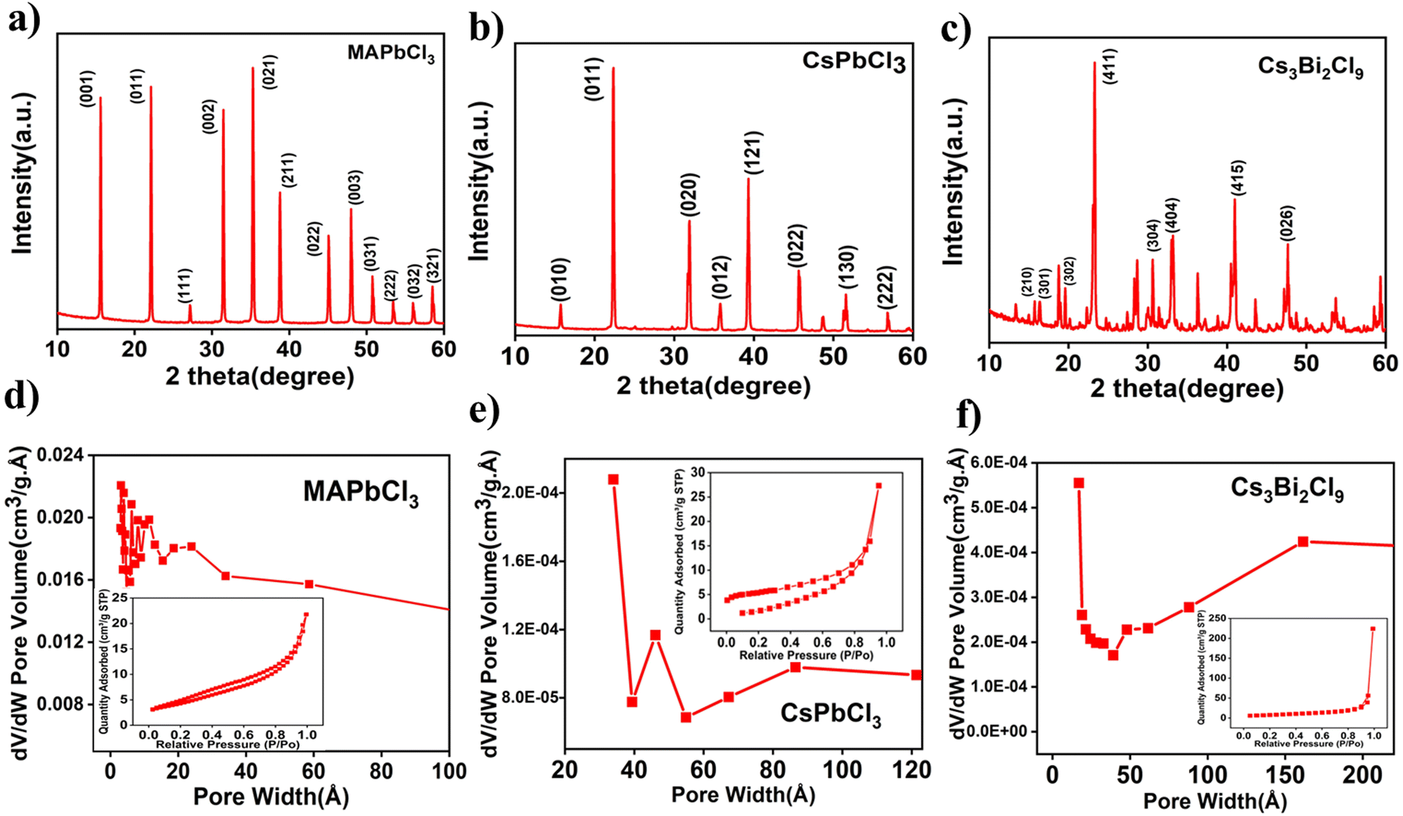 | ||
| Fig. 1 Powder XRD of (a) MAPbCl3, (b) CsPbCl3 and (c) Cs3Bi2Cl9. BET surface area measurement of (d) MAPbCl3, (e) CsPbCl3 and (f) Cs3Bi2Cl9. | ||
Field emission scanning electron microscopy (FESEM) was used to analyse the surface morphology of the perovskite electrodes, as shown in Fig. S1 (ESI†). FESEM images show the presence of macropores in the perovskite samples. The benefit of having macropores is that they help in reducing the electrolyte ion diffusion distance to the active sites and lowering the ion transport resistance, which facilitates the development of a more effective electrical double layer.38 The thermal stability of the synthesized perovskite powders was tested by thermogravimetric analysis (TGA). The perovskite powders were heated from room temperature to 800 °C with an increment of 10 °C min−1 in the presence of a nitrogen atmosphere. MAPbCl3 shows the first stage of loss of mass (exothermic reaction) around 260 °C (Fig. S2, ESI†), while cesium-based inorganic perovskites are comparatively more thermally stable than mixed organic inorganic perovskites (MAPbCl3) with the first exothermic reaction at around 450 °C for Cs3Bi2Cl9 and 600 °C for CsPbCl3. In the case of MAPbCl3/CsPbCl3, the first thermal event corresponds to reaction
| MAPbCl3/CsPbCl3 (s) → MACl/CsCl (s) + PbCl2 (s) |
In the case of Cs3Bi2Cl9, weight loss started at approximately 450 °C, then sharply increased after 590 °C, corresponding to the boiling of BiCl3. Therefore, both inorganic and lead-free perovskites are stable over a wide temperature range of operation.
XPS analysis
To understand the structural aspects of the electrode materials, we have performed X-ray photoelectron spectroscopy (XPS), especially lead-free Cs3Bi2Cl9 perovskite powder and the as prepared electrode. The full scan XPS spectra of the synthesized Cs3Bi2Cl9 powder and as prepared electrode are shown in Fig S3 (ESI†). In Fig. 2 the XPS spectra of the constituent elements Cs, Bi and Cl are shown for the synthesized powder as well as for the as prepared electrode. It should be noted that some carbon and oxygen are present in the pure perovskite powder due to trapped gases and moisture during synthesis. The major difference observed in the XPS spectrum of bismuth is the existence of mixed states in pure perovskite powder due to which there are four peaks in the XPS spectrum. This could be due to the presence of Bi2O3 apart from BiCl3. After mixing with carbon super P and PVDF in acetonitrile solvent, two of the peaks disappear in the electrode materials. There is a shift (∼1 ev) observed in Bi3+ peak position possibly due to the formation of BiF3. We have also observed the broadening of the Cl 2p peaks after electrode preparation. A similar trend is also observed for the Cs and Cl spectrum. The number of peaks decreases while the binding energies increase. | ||
| Fig. 2 XPS analysis spectra of the as-synthesized powder (a) Bi 4f, (b) Cl 2P and (c) Cs 3d and the as prepared electrode (d) Bi 4f, (e) Cl 2P and (f) Cs 3d of the Cs3Bi2Cl9 perovskites. | ||
Electrochemical measurement
The as-prepared perovskite samples were used as electroactive materials to investigate their electrochemical performances in a three-electrode system. Galvanostatic charge/discharge (GCD) cycling was used to calculate the capacitance, energy, and power density of the materials using the discharge side of the curve. There is a negligible voltage drop in the GCD test results. The charging and discharging behaviour in Fig. 3a departs from an isosceles triangle, which is a result of pseudo capacitance. The specific capacitance (F g−1), energy density (W h kg−1) and power density (W kg−1) can be calculated from eqn (S1)–(S3) in the ESI.† Lead-free perovskite Cs3Bi2Cl9 shows the highest specific capacitance around 175 F g−1 at 0.2 A g−1 current density compared to lead-based perovskite materials. Due to the diffusion effect limiting the movement of the electrolytic ions at higher current densities, some active surface areas of the electrode become inaccessible for storing charge at high current densities. Consequently, electrochemical reactions only occur at the surface and that results in a decrease in the specific capacitance value, as shown in Fig. 3b. However, with a low current density, the ions have enough time to penetrate into the interior part of the electrode, allowing the entire electrode material to participate in the electrochemical process.39 This process should be reversible to achieve long cycle life of the supercapacitors. Another interesting thing is observed at higher current densities (above 0.5 A g−1); CsPbCl3 has a higher value of capacitance than the other two perovskite electrode materials. Lead-free perovskite also shows a higher window than the other two lead-based perovskites. Cs3Bi2Cl9 exhibits the highest energy density of 103 W h kg−1 at 0.2 A g−1 and a power density of around 700 W g−1 at 0.7 A g−1 current density. A similar trend for energy density as shown in Fig. 3c was also observed at higher current density. It can be seen from Fig. 3d that the power density increases almost linearly with respect to current density. In comparison to MAPbCl3 and CsPbCl3, lead-free perovskite has a slightly higher power density. Fig. 3e shows the comparison of the cyclic voltammetry curves of the perovskite electrode over an applied scan rate of 5 mV s−1. Eqn (S4) (ESI†) can be used to calculate the specific capacitance from the CV curve. In each CV curve, there is a prominent redox peak, indicating that the capacitance is primarily based on redox processes. The peak current increases almost linearly with scan rate (Fig. S4, ESI†), demonstrating high electrochemical capacitance, interfacial faradaic redox reactions, and rapid electron and ion transport rates.40 Furthermore, symmetrical CV curves were obtained even with increased scan speeds, indicating the synthesized materials' strong ion and electron conduction. To understand the electrochemical charge storage mechanism, the CV curves can be fitted by using the power-law relationship as given by the equation below,| ip = kvb | (1) |
![[thin space (1/6-em)]](https://www.rsc.org/images/entities/char_2009.gif) ipvs. logv graph was used to calculate the b-value. The capacitive and/or diffusive contributions can be calculated using the above relationship. The capacitive response is more likely to be diffusion dominated (behaving like a battery) if the b-value is closer to 0.5. The electrode's surface reactions are more likely to be capacitive-dominated if the b-value is closer to 1.41 Fig. S5 (ESI†) illustrates the plots of logv (scan rate) vs. logip for each electrode by the relationship (eqn (1)). The b-values of MAPbCl3, CsPbCl3, and Cs3Bi2Cl9, obtained from the slope of the linear fits, are 0.82, 0.57, and 0.88, respectively, at 0V. The b-values of the MAPbCl3 and Cs3Bi2Cl9 electrodes are in the range of 0.5 and 1, but are comparatively closer to 1, showing that the charge storage mechanism is a combination of capacitive and diffusive response, with a significantly higher contribution from capacitive response in the low voltage regime. In the case of the CsPbCl3 electrode, the relatively lower b-value indicates a relatively large contribution from diffusion-controlled processes. It can also be observed from Fig. S5 (ESI†) that at higher potential, the b value for MAPbCl3 and Cs3Bi2Cl9 decreases, which indicates that the charge storage mechanism is mainly diffusion limited at higher applied bias. The relatively stable b-value for CsPbCl3 indicates that the charge storage is independent of applied bias.
ipvs. logv graph was used to calculate the b-value. The capacitive and/or diffusive contributions can be calculated using the above relationship. The capacitive response is more likely to be diffusion dominated (behaving like a battery) if the b-value is closer to 0.5. The electrode's surface reactions are more likely to be capacitive-dominated if the b-value is closer to 1.41 Fig. S5 (ESI†) illustrates the plots of logv (scan rate) vs. logip for each electrode by the relationship (eqn (1)). The b-values of MAPbCl3, CsPbCl3, and Cs3Bi2Cl9, obtained from the slope of the linear fits, are 0.82, 0.57, and 0.88, respectively, at 0V. The b-values of the MAPbCl3 and Cs3Bi2Cl9 electrodes are in the range of 0.5 and 1, but are comparatively closer to 1, showing that the charge storage mechanism is a combination of capacitive and diffusive response, with a significantly higher contribution from capacitive response in the low voltage regime. In the case of the CsPbCl3 electrode, the relatively lower b-value indicates a relatively large contribution from diffusion-controlled processes. It can also be observed from Fig. S5 (ESI†) that at higher potential, the b value for MAPbCl3 and Cs3Bi2Cl9 decreases, which indicates that the charge storage mechanism is mainly diffusion limited at higher applied bias. The relatively stable b-value for CsPbCl3 indicates that the charge storage is independent of applied bias.
 | ||
| Fig. 3 (a) Galvanostatic charge discharge (GCD) measurement for all three electrodes, (b) specific capacitance, (c) energy density, (d) power density, (e) cyclic voltammetry and (f) Nyquist plot of all three electrodes. Inset: High frequency semicircle. | ||
To further understand the electrochemical behavior of the perovskite electrodes, Fig. 3f shows the Nyquist plots obtained through electrochemical impedance spectroscopy. The intercept of the curves with the horizontal axis presents the charge transfer resistance (CTR). According to the inset of Fig. 3f, the CTRs of the MAPbCl3, CsPbCl3, and Cs3Bi2Cl9 electrodes are 20 Ω, 16 Ω and 11 Ω, respectively. The ratio of the dielectric loss factor ε′′ to the dielectric constant ε′ is defined as the loss tangent and is given by
| tanδ = ε′′/ε′ | (2) |
As shown in Fig. S6a (ESI†), the loss tangent curve for the perovskite electrodes is given as a function of frequency. It is evident from the plot that tanδ increases with frequency, reaching a maximum value at frequency fm, and then declines in the high-frequency zone. Since the ohmic resistance was more important than the reactance component for the capacitance of the dipole charges at low frequencies, tanδ increases as frequency increases.42 On further increase in frequency to the MHz regime, tanδ decreases because the reactance component increases proportionately to frequency but the ohmic portion does not change with frequency. The calculated value of the diffusion coefficient from the loss tangent plot lies in the range of 10−14–10−16 m2 s−1 for perovskite electrodes. The Einstein equation D = μkBT, where D is the diffusion coefficient, μ is the mobility, kB is Boltzmann's constant, and T is the absolute temperature, can also be used to determine ionic mobility. It can be observed from Fig. S6b (ESI†) that the mobility of lead-free perovskite Cs3Bi2Cl9 is slightly less than that of MAPbCl3 but higher than that of CsPbCl3. Ionic mobility does not significantly change with a bias applied. Jonscher's power law was used to calculate the ionic conductivity of perovskite by the equation σion = ε0ε′′ω.43 For Cs3Bi2Cl9 electrodes, the highest ionic conductivity (Fig. S6c, ESI†) is observed at ambient temperature among all samples. Higher ionic conductivity in lead-free Cs3Bi2Cl9 electrodes results in higher specific capacitance and energy density.
 | ||
| Fig. 4 XRD pattern of CsCl, BiCl3 and Cs3Bi2Cl9 powder and electrode (as prepared, after charging and after discharging). | ||
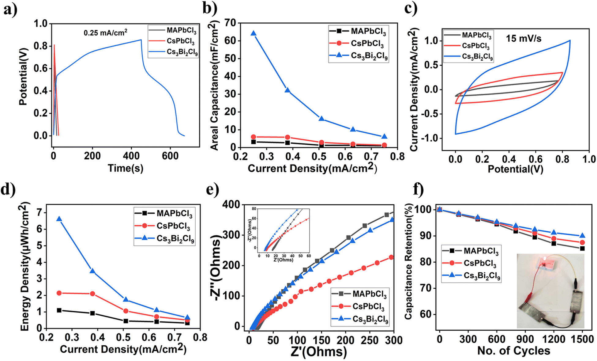 | ||
| Fig. 5 (a) GCD measurement data, (b) calculated areal capacitance, (c) cyclic voltammetry measurement, (d) energy density, (e) Nyquist plots of various devices and (f) cyclic stability measurement. Inset: Working device. | ||
The fundamental charge-transfer kinetics that occurs at the electrode/electrolyte interface region was examined using the EIS analysis of various perovskite supercapacitor devices, and the results were analysed using a Nyquist plot, as shown in Fig. 5e. A small semicircle that results from charge transfer resistance can be seen in the high-frequency area of the Nyquist plot. The lead-free Cs3Bi2Cl9 supercapacitor device exhibited a small equivalent series resistance (Resr) of about 7 Ω followed by CsPbCl3 and MAPbCl3 with Resr 9 Ω and 15 Ω, respectively. The Bode magnitude and Bode phase plots of various devices are shown in Fig. S10 (ESI†). A cycling stability test was performed to evaluate the electrochemical performance of the various perovskite devices. Fig. 5f shows that the capacitance retention of the Cs3Bi2Cl9 device is up to 90% after 1500 cycles, which is the highest among the various perovskite devices tested here. We have also demonstrated working devices where two ASCs are used in series to drive a red light-emitting diode, indicating their practical applications in thin film-based energy storage devices.
 | ||
| Fig. 6 (a) Substrate bending during bending angle measurement; variation of areal capacitance and corresponding fitted data (b) with bending angles, (c) with bending cycles and (d) substrate twisting during twisting angle measurements; variation of areal capacitance (e) with twisting angles and (f) with twisting cycles. | ||
In the ESI† Fig. S6b (inset shows CV curves at different bending angles) represents the change in areal capacitance of a flexible device with a linear stage. The device retains around 93% of the initial capacitance after a 180° bending angle. Cycling stability was also tested for bending cycles and the device retains 89% of the initial capacitance. We have fitted linearly and exponentially for the bending angle and bending cycles, respectively. The fitting parameters for bending angle and bending cycle are shown in Tables S1 and S2 in the ESI.† It is observed that the device reaches a steady state value at 89% after 200 bending cycles while there is a characteristic bending cycle of 30. Twisting angle and twisting cycle tests were performed with an angular stage setup. The device retains approx. 86% of the initial areal capacitance after 120° twisting angles (Fig. 6e) and 83% (Fig. 6f) after 200 twisting cycles. Tables S3 and S4 in the ESI† show the fitting parameters of twisting angle and cycling stability measurement data. The steady state value reaches 82% after 200 twisting cycles while the characteristic twisting cycle is ∼76. However, twisting angle results in faster degradation of the device compared to the bending angle. The relative decrease in device performance during bending and twisting angle and cycle measurement is due to the crack formation and delamination of the active electrode with SS substrates. Therefore, interface engineering is necessary for further improvement of the stability of these flexible thin film supercapacitors.
Conclusion
In conclusion we have successfully fabricated high performance thin film flexible supercapacitors of lead-free halide perovskite Cs3Bi2Cl9 having areal capacitance 64 mF cm−2 at an energy density over 6.5 μW h cm−2 for a mass loading of 1 mg cm−2. Areal capacitance is 8–10 times higher, while energy density is 3–4 times higher than the lead-based perovskites such as MAPbCl3 and CsPbCl3. The improved performance is due to the increased specific surface area as well as higher ionic conductivity in lead-free perovskites compared to lead-based perovskites. The charge storage mechanism in these devices is mostly capacitive at the low applied bias while it is diffusion dominated at higher applied bias voltage. Ex situ XRD measurement reveals the reorganization of ions during Li-intercalation, which results in additional XRD peaks after charging. No such changes are observed in MAPbCl3 or CsPbCl3-based devices during charging or discharging cycles. We have demonstrated the flexibility of these thin film devices over a wide range of up to 180° for bending and 120° for twisting angle. These devices are also stable over 200 bending and twisting cycles. Therefore, lead-free halide perovskites could be potential candidates for thin film flexible supercapacitors as energy storage devices in portable electronics.Experimental methods
Materials used
The materials used in this study consist of lead chloride(II) (99.9%, Sigma Aldrich), cesium chloride (CsCl), 99% SRL Chemicals, methylammonium chloride (98%, TCI Chemicals), and dimethylformamide (DMF, anhydrous 99.8%, Sigma Aldrich), bismuth chloride (99%, Sigma Aldrich), acetonitrile (99%, SRL Chemicals), lithium bis(trifluoromethane sulfonic)imide (99%, Sigma Aldrich), polyvinyl alcohol (99%, Sigma Aldrich).Synthesis of perovskite powder
We have used a single-step method of obtaining perovskite powder for supercapacitor applications. Some perovskite powder can be obtained within a few minutes, which is otherwise 8–10 hours to obtain the powder by grinding synthesized single crystals.For MAPbCl3 perovskite powder, 0.5 M MACl, and 0.7 M PbCl2 were dissolved in mixed solvent DMF and DMSO (7:3). The solution was filtered with a 0.2 μm PTFE syringe filter and then 1 mL acetonitrile (ACN) was added into the precursor solution and put at the hot plate at 60 °C.
For CsPbCl3 perovskite powder, 0.5 M CsCl and 0.7 M PbCl2 were dissolved in DMF and stirred for 30 minutes. The solution was filtered with a 0.2 μm PTFE syringe filter and 200 μL mL acetonitrile (ACN) was added to the precursor solution. The solution was kept on a hot plate at 60 °C for 30 minutes. Perovskite powder was obtained, excess solution was removed from the glass vial, and powder was dried on a hot plate at 60 °C for 15 minutes.
For Cs3Bi2Cl9 lead-free perovskite powder, 1.2 M CsCl and 1 M BiCl3 were dissolved in DMF and sonicated for 15 minutes. The solution was filtered, and 200 μL acetonitrile was added to the precursor solution. After that, the solution was put on a hot plate at 75 °C for 30 minutes. The excess solution was removed from the voil, and the powder was dried at 70 °C for 15 minutes.
Material characterization
An X-ray diffractometer (XRD D8-Advance) with Cu K = 1.54 Å was used to characterize the synthesized perovskite powder for structural information in the angle range of 10°–60°. Using a field emission scanning electron microscope, morphological characterization of the perovskite powder was performed (FE-SEM QUANTA 200 FEG). A Quanta chrome BET surface analyser was used to get the surface area of the perovskite powder. The detailed analysis of the surface elemental components of the prepared electrodes has been done by X-ray photoelectron spectroscopy (XPS) (PHI 5600 Versa Probe III).Electrode fabrication and electrochemical measurement
The active perovskite powder electrodes were prepared by mixing the synthesized perovskite material (MAPbCl3 or CsPbCl3 or Cs3Bi2Cl9: 70%), binder (PVDF: 15%), and activated carbon (Super P: 15%) in a sufficient amount of NMP solvent. To make a homogenous slurry, the solution was agitated for 12 hours. The homogenous slurry was then uniformly coated onto a graphite sheet (1 × 0.8 cm2), and the coated electrodes were then dried in a vacuum oven at 80 °C for 12 hours. The loaded active ingredients on the electrodes weigh about 1 mg (approx.).A three-electrode system was used (Auto-lab potentiostat/galvanostat electrochemical analyzer), which includes a perovskite working electrode, a counter electrode (Pt), and a reference electrode (Ag/AgCl) in an electrolyte solution. 0.1 M LiTFSi in acetonitrile was used as the liquid electrolyte.
Gel electrolyte-based device fabrication
Solid state thin film supercapacitor devices have been fabricated by preparing a quasi-solid gel electrolyte, which can be sandwiched between two active electrodes. To prepare the PVA/LiTFSi gel electrolyte, an appropriate amount of PVA was dissolved in DI water, and then 0.1 M LiTFSi electrolyte solution was added and continuously stirred until a gel paste was formed. After that, the Cs3Bi2Cl9 perovskite electrode and activated carbon electrode were sandwiched to form the asymmetric supercapacitor (ASC) device. Using a PVA/LiTFSi gel electrolyte as the electrolyte medium, both electrodes are put face to face without a separator. To protect it from outside moisture, the device was wrapped with parafilm.Abbreviations
| 3D | 3 Dimensional |
| 2D/3D | Quasi 2 dimensional |
| HPs | Halide perovskites. |
Funding sources
The work is supported by the Science and Engineering Research Board (SERB), Department of Science and Technology, India under the award no. CRG/2021/001744 dated 07/03/2022.Conflicts of interest
There are no conflicts to declare.Acknowledgements
MB acknowledges Science and Engineering Research Board, Department of Science and Technology, India under the award no. CRG/2021/001744 dated 07/03/2022 for partial support. A. Y. acknowledges Council of Scientific and Industrial Research (CSIR), New Delhi for PhD fellowship. A. S. and P. K. acknowledge Ministry of Education, Government of India for PhD fellowship. A. Y. acknowledges Tinkering Laboratory, IIT Roorkee for providing 3D printing facilities to develop the linear and angular stage.References
- A. Elgendy, N. M. El Basiony, F. El-Taib Heakal and A. E. Elkholy, J. Power Sources, 2020, 466, 228294 CrossRef CAS.
- A. E. Elkholy, F. El-Taib Heakal and N. K. Allam, RSC Adv., 2017, 7, 51888–51895 RSC.
- G. A. Olah, A. Goeppert and G. K. S. Prakash, J. Org. Chem., 2009, 74, 487–498 CrossRef CAS.
- A. Vlad, N. Singh, J. Rolland, S. Melinte, P. M. Ajayan and J. F. Gohy, Sci. Rep., 2014, 4, 1–7 Search PubMed.
- L. Kouchachvili, W. Yaïci and E. Entchev, J. Power Sources, 2018, 374, 237–248 CrossRef CAS.
- W. Cheng, J. Fu, H. Hu and D. Ho, Adv. Sci., 2021, 8, 1–13 Search PubMed.
- T. Schoetz, L. W. Gordon, S. Ivanov, A. Bund, D. Mandler and R. J. Messinger, Electrochim. Acta, 2022, 412, 140072 CrossRef CAS.
- P. Sun, C. Wang, W. He, P. Hou and X. Xu, ACS Sustain. Chem. Eng., 2017, 5, 10139–10147 CrossRef CAS.
- C. Ogata, R. Kurogi, K. Hatakeyama, T. Taniguchi, M. Koinuma and Y. Matsumoto, Chem. Commun., 2016, 52, 3919–3922 RSC.
- A. E. Elkholy, F. E. Heakal and N. K. Allam, Electrochim. Acta, 2019, 296, 59–68 CrossRef CAS.
- A. Mahapatra, D. Prochowicz, M. M. Tavakoli, S. Trivedi, P. Kumar and P. Yadav, J. Mater. Chem. A, 2020, 8, 27–54 RSC.
- Y. Zu, J. Dai, L. Li, F. Yuan, X. Chen, Z. Feng, K. Li, X. Song, F. Yun, Y. Yu, B. Jiao, H. Dong, X. Hou, M. Ju and Z. Wu, J. Mater. Chem. A, 2019, 7, 26116–26122 RSC.
- N. Wang, L. Cheng, R. Ge, S. Zhang, Y. Miao, W. Zou, C. Yi, Y. Sun, Y. Cao, R. Yang, Y. Wei, Q. Guo, Y. Ke, M. Yu, Y. Jin, Y. Liu, Q. Ding, D. Di, L. Yang, G. Xing, H. Tian, C. Jin, F. Gao, R. H. Friend, J. Wang and W. Huang, Nat. Photonics, 2016, 10, 699–704 CrossRef CAS.
- R. Kumar, J. Kumar, P. Srivastava, D. Moghe, D. Kabra and M. Bag, ACS Appl. Mater. Interfaces, 2020, 12, 34265–34273 CrossRef CAS PubMed.
- A. Mahapatra, V. Anilkumar, R. D. Chavan, P. Yadav and D. Prochowicz, ACS Photonics, 2023, 10, 1424–1433 CrossRef CAS.
- A. Mahapatra, D. Prochowicz, J. Kruszyńska, S. Satapathi, S. Akin, H. Kumari, P. Kumar, Z. Fazel, M. M. Tavakoli and P. Yadav, J. Mater. Chem. C, 2021, 9, 15189–15200 RSC.
- N. Tewari, D. Lam, C. H. A. Li and J. E. Halpert, APL Mater., 2022, 10, 040905 CrossRef CAS.
- S. Narayanan, N. Parikh, M. M. Tavakoli, M. Pandey, M. Kumar, A. Kalam, S. Trivedi, D. Prochowicz and P. Yadav, Eur. J. Inorg. Chem., 2021, 1201–1212 CrossRef CAS.
- R. Kumar and M. Bag, J. Phys. Chem. C, 2021, 125, 16946–16954 CrossRef CAS.
- R. Kumar and M. Bag, Energy Technol., 2022, 10, 2100889 CrossRef CAS.
- A. Yadav, P. S. Shukla, A. Suhail, J. Kumar and M. Bag, ACS Appl. Nano Mater., 2023, 6, 16960–16969 CrossRef CAS.
- H. Huang, M. I. Bodnarchuk, S. V. Kershaw and M. V. Kovalenko, ACS Energy Lett., 2017, 9, 2071–2083 CrossRef.
- X. Li, X. Gao, X. Zhang, X. Shen, M. Lu, J. Wu, Z. Shi, V. L. Colvin, J. Hu, X. Bai, W. W. Yu and Y. Zhang, Adv. Sci., 2021, 8, 2003334 CrossRef CAS PubMed.
- S. Y. Kim and H. Won, J. Mater. Chem. C, 2019, 7, 5226–5234 RSC.
- F. Giustino and H. J. Snaith, ACS Energy Lett., 2016, 1, 1233–1240 CrossRef CAS.
- W. Ke and M. G. Kanatzidis, Nat. Commun., 2019, 1–4 CAS.
- P. K. Nayak, M. Sendner, B. Wenger, Z. Wang, K. Sharma, A. J. Ramadan, R. Lovrinčić, A. Pucci, P. K. Madhu and H. J. Snaith, J. Am. Chem. Soc., 2018, 140, 574–577 CrossRef CAS PubMed.
- A. Swarnkar, V. K. Ravi and A. Nag, ACS Energy Lett., 2017, 2, 1089–1098 CrossRef CAS.
- Q. Huang, C. Tian, J. Lai, F. Qi, N. Zhang, J. Liu, Z. Liang, D. Wu and X. Tang, Inorg. Chem., 2022, 61, 14447–14454 CrossRef CAS PubMed.
- L. Qian, Y. Sun, M. Wu, C. Li, D. Xie, L. Ding and G. Shi, Nanoscale, 2018, 10, 6837–6843 RSC.
- S. Beniwal, A. Kumar, R. Kumar, A. Suhail and M. Bag, J. Phys. Chem. C, 2023, 127, 12874–12881 CrossRef CAS.
- G. Maculan, A. D. Sheikh, A. L. Abdelhady, M. I. Saidaminov, A. Haque, B. Murali, E. Alarousu, O. F. Mohammed, T. Wu and O. M. Bakr, J. Phys. Chem. Lett., 2015, 6, 3781–3786 CrossRef CAS.
- P. Jyoti, S. Rana, T. Swetha, H. Mandal, A. Saeki, P. R. Bangal and S. P. Singh, J. Phys. Chem. C, 2019, 123, 17026–17034 CrossRef.
- N. K. Tailor and S. Satapathi, Integr. Med. Res., 2020, 9, 7149–7157 CAS.
- P. Sagar, A. Agrawal, A. Gaur and G. D. Varma, J. Energy Storage, 2023, 59, 106580 CrossRef.
- S. K. Meher and G. R. Rao, J. Phys. Chem. C, 2011, 115, 15646–15654 CrossRef CAS.
- D. V. Chernysheva, Y. A. Chus, V. A. Klushin, T. A. Lastovina, L. S. Pudova, N. V. Smirnova, O. A. Kravchenko, V. M. Chernyshev and V. P. Ananikov, ChemSusChem, 2018, 11, 3599–3608 CrossRef CAS.
- B. Thomas, S. Geng, M. Sain and K. Oksman, Nanomaterials, 2021, 11, 653 CrossRef CAS PubMed.
- S. Verma, B. Padha, A. Singh, S. Khajuria, A. Sharma, P. Mahajan, B. Singh and S. Arya, Fullerenes, Nanotubes Carbon Nanostruct., 2021, 29, 1045–1052 CrossRef CAS.
- K. Li, B. Zhao, H. Zhang, H. Lv, J. Bai, H. Ma, P. Wang, W. Li, J. Si, X. Zhu and Y. Sun, Adv. Funct. Mater., 2021, 31, 2103073 CrossRef CAS.
- A. Yadav, P. S. Shukla, J. Kumar, G. Das Varma and M. Bag, Energy Technol., 2022, 10, 2200778 CrossRef CAS.
- S. Ghosh, J. S. Kumar, N. Chandra, R. S. Ganesh, H. Inokawa and T. Kuila, Composites, Part B, 2019, 177, 107373 CrossRef CAS.
- P. Srivastava, R. Kumar and M. Bag, Phys. Chem. Chem. Phys., 2021, 23, 10936–10945 RSC.
- L. Wang, H. Yao, F. Chi, J. Yan, H. Cheng, Y. Li, L. Jiang and L. Qu, ACS Nano, 2022, 16, 12813–12821 CrossRef CAS.
- A. Inman, T. Hryhorchuk, L. Bi, J. Wang, B. Greenspan, T. Tabb, E. M. Gallo, A. Vahidmohammadi, G. Dion and Y. Gogotsi, J. Mater. Chem. A, 2023, 11, 3514–3523 RSC.
- X. Li, J. Shao, S. K. Kim, C. Yao, J. Wang, Y. R. Miao, Q. Zheng, P. Sun, R. Zhang and P. V. Braun, Nat. Commun., 2018, 9, 2578 CrossRef.
Footnote |
| † Electronic supplementary information (ESI) available. See DOI: https://doi.org/10.1039/d3tc02784h |
| This journal is © The Royal Society of Chemistry 2024 |