
 Open Access Article
 This Open Access Article is licensed under a Creative Commons Attribution-Non Commercial 3.0 Unported Licence
Thermoelectric Zintl phases with ultralow thermal conductivity: synthesis, structural characterization, and transport properties of Ca10AlSb9 and Ca10CdSb9†
Kowsik
Ghosh
 a,
Leah
Borgsmiller
b,
Sviatoslav
Baranets
ac,
G. Jeffrey
Snyder
*b and
Svilen
Bobev
*a
a,
Leah
Borgsmiller
b,
Sviatoslav
Baranets
ac,
G. Jeffrey
Snyder
*b and
Svilen
Bobev
*a
aDepartment of Chemistry and Biochemistry, University of Delaware, Newark, Delaware 19716, USA. E-mail: bobev@udel.edu
bDepartment of Materials Science and Engineering, Northwestern University, Evanston, IL 60208, USA. E-mail: jeff.snyder@northwestern.edu
cDepartment of Chemistry, Louisiana State University, Baton Rouge, Louisiana 70803, USA
First published on 2nd September 2024
Abstract
Two new Zintl antimonides, Ca10MSb9 (M = Al and Cd), have been synthesized and characterized for the first time and their thermoelectric performance has been evaluated without additional optimization. The two phases can be readily synthesized either by Sn-flux or direct solid-state reactions. The compounds are isotypic and crystallize in a tetragonal crystal system with the space group P42/mnm (no. 136). The crystal structure is highly complex with significant structural disorder—both occupational and positional. For its careful elucidation, both single-crystal X-ray diffraction methods and Rietveld refinements of powder X-ray diffraction data for polycrystalline bulk samples were required. Despite the significant disorder, the structures retain their charge balance and these new Zintl phases are shown to be intrinsic semiconductors with a bandgap of about 0.5 eV. High-temperature transport measurements reveal remarkably low thermal conductivity (0.6–0.7 W m−1 K−1) in the temperature range 323 K to 573 K, which is even lower than that of the well-known thermoelectric Zintl material Yb14MnSb11. Additionally, Seebeck coefficient measurements showed a very high value for Ca10AlSb9, approaching 350 μV K−1 at 573 K. Therefore, we speculate that with proper systematic work and further optimization, these and potentially other Zintl compounds from this extended family can show excellent thermoelectric performance.
1. Introduction
Thermoelectric materials play an irreplaceable role in power generation for deep space exploration missions1,2 by helping generate electricity for probes and rovers using a temperature gradient. The efficiency of the energy conversion ability of such materials can be estimated from the dimensionless figure of merit, zT = S2T/ρκ, where ρ is the electrical resistivity, S is the Seebeck coefficient (also referred to as the thermopower), and κ is the thermal conductivity. From the zT expression, it is clear that improving the thermoelectric performance of a given material, i.e., enhancing the zT value, can be achieved by increasing the Seebeck coefficient and/or decreasing the electrical resistivity and thermal conductivity. However, accomplishing this task is challenging due to the mutual relationship between these material properties, which are all influenced by the charge carrier concentration. As such, good thermoelectric materials must have high charge carrier concentrations (∼1020 cm−3), which in turn cause the electrical resistivity to decrease, but can lead to an increase in the thermal conductivity. Often, high charge carrier concentrations can cause lowering of the Seebeck coefficient (generally optimal zT occurs when S ∼200–250 μV K−1).1–4Zintl phases are a class of materials that in the past 15 years have been explored as promising candidates for thermoelectric applications.5–9 A key feature of Zintl phases is the coexistence of covalent bonding (within the polyanionic sub-lattice) and ionic interactions (between the cations and anions), which allows us to consider the structures as formed from species with stable valence-shell electron configurations.6,9,10 As a result, many Zintl phases show intrinsic semiconducting behavior. Considering that optimal electrical transport properties are realized in semiconducting materials that are (can be) heavily doped, one can understand the increased attention towards such compounds. Additionally, structural complexity, which is the norm for many Zintl phases, can lead to low lattice thermal conductivity.6,9–13 Therefore, it can be expected that such a combination of structural features/properties may contribute to high zT values.
Most of the Zintl phases related to the development of thermoelectric materials belong to the families of tetrelides (based on the elements of group 14) and pnictides (based on the elements of group 15). Among them, the phases with the general chemical formula Yb14MSb11 (M = Mn, Mg, Zn, Al)14–18 are known as some of the highest performing thermoelectric materials in the high-temperature regime. They share something in common—all have inherently low and glass-like thermal conductivity,15–17 which can lead to zT values as high as 1.3 at 1223 K for Yb14Mn1−xAlxSb11.17 Some other examples of Zintl pnictides with high thermoelectric performance are AE3MSb3 (AE = Ca, Sr; M = Al, Ga),19–21 clathrates,7,22–24 skutterudites,25,26 Mg3Sb2,27–29 AEM2Pn2 (AE = alkaline-earth metal, Yb, Eu; M = Mg, Mn, Zn, Cd; Pn = Sb, Bi),30–39 AE5M2Sb6 (AE = Ca, Sr; M = Al, Ga),40–45 and A9M4+xSb9 (A = Ca, Yb; M = Zn, Mn, Cd).46–49 The electrical transport properties of some of those materials can be easily tuned by appropriate chemical doping, and the thermal conductivities can be reduced by the introduction of disorder into their crystal structures.
At this point, one should recall that phonon scattering within Zintl phases can be enhanced (thereby decreasing the lattice thermal conductivity) either by heavy atoms, which reduce the phonon velocity (thereby indirectly increasing scattering), or by introducing substitutional disorder via iso- and alio-valent substitutions in either cationic or anionic sites. In all cases, structural disorder is created, which adds to the complexity of the chemical bonding. With reference to that, we can cite results from our own recent studies that have shown enhanced thermopower in (Ca,RE)9Cd4Sb9![[thin space (1/6-em)]](https://www.rsc.org/images/entities/char_2009.gif) 50 and Ca10RECdSb951 phases (RE = rare-earth metal), where heavy rare-earth elements substitute the light Ca. Another example of substitutional disorder leading to enhanced thermoelectric performance is the case of Li and Cd co-doping in Mg3Sb2.52
50 and Ca10RECdSb951 phases (RE = rare-earth metal), where heavy rare-earth elements substitute the light Ca. Another example of substitutional disorder leading to enhanced thermoelectric performance is the case of Li and Cd co-doping in Mg3Sb2.52
The crystal structures with naturally “built-in” disorder and complexity of some Zintl phases can be a great starting point for the optimization of their transport properties. For instance, the newly discovered Zintl pnictides AE10MSb9 (AE = Ca, Yb; M = Ga, In, Mn, Zn),53–57 known as “10-1-9” phases, have all shown ultralow thermal conductivity due to the complex disorder in their crystal structures. One should be reminded that the abbreviated “10-1-9” formula is deceptively simplified (and may imply similarities with the Zintl “11-1-9” phases such as Yb11GaSb9, Yb11InSb9, Yb11AlSb9, and Eu11InSb9,58–61 which is not true as their structures are distinctly different), since it does not indicate the disorder on multiple sites—the actual formula, which can be presented as AE10+x+yM1−ySb9, serves this purpose better, but is too complicated and seldom used in colloquial descriptions/writing. Because of the inherent disorder, the structure is amenable to doping. For example, the sodium doped Yb10MgSb9 samples have shown an enhanced zT value of 1 at 800 K, which is even higher than that of Yb14MnSb11 at that temperature.53 Therefore, it is not surprising that some of the “10-1-9” phases we reported not long ago have caught attention and are now being developed as new thermoelectric materials.53–57
In this contribution, we describe the synthesis, structural characterization and transport properties of new members of the “10-1-9” family, Ca10+x+yM1−ySb9 (0 < x < 0.5, 0 < y < 0.68; M = Al, Cd). As indicated already, for the sake of simplicity, the formula Ca10MSb9 will be used hereafter. We present the results of synthesis of both single crystals and powder samples and the structural characterization of these new materials, which was carried out via single-crystal X-ray diffraction methods and complemented by Rietveld refinements from powder X-ray diffraction data. The highly disordered structures can be rationalized using the Zintl concept.62,63 TB-LMTO-ASA calculations for an idealized, disorder-free Ca11CdSb9 structure were done and helped reveal some of the details of the nature of chemical bonding. Thermoelectric property measurements on the as-synthesized samples suggest that these materials can be an excellent starting point for zT optimization and the development of new thermoelectrics.
2. Experimental section
2.1 Synthesis
Single crystals of Ca10MSb9 (M = Al, Cd) were grown by the Sn flux method, and polycrystalline samples were made by the solid-state direct reaction method. All work was carried out under a protective atmosphere or under vacuum since both the starting materials and the products are moderately air-sensitive. The elements Ca, Cd/Al, Sb, and Sn were purchased from Sigma-Aldrich and Alfa-Aesar with a purity of ≥99.9% wt. In a typical flux-growth experiment, elemental Ca, Cd, Sb and Sn mixtures were loaded into a 2 cm3 alumina crucible (with the ratio Ca:Cd:Sb:Sn = 5:1:9:70). The crucible was then covered with a piece of quartz wool and sealed in an evacuated fused silica tube. The following heat treatment was then applied: (1) heating to 500 K (rate: 100 K h−1) with a subsequent 6 h dwelling; (2) heating to 1273 K (rate: 100 K h−1); (3) equilibration at this temperature for 12 h; and (4) cooling to 1023 K (rate: 5 K h−1). At that point, the tube can be taken out of the muffle furnace, allowing the Sn flux to be separated from the solid (done by centrifugation). Since the grown crystals are not stable in ambient air, upon separation of the molten metal flux from the solid product, the sealed tube must be transferred to a glove box and then opened.
Safety note: high-temperature centrifugation is a relatively simple process, but it is associated with a risk for injury and must be performed with proper personal protective equipment: fireproof clothing, heat-resistant gloves, and a face shield.
Bulk powders of Ca10AlSb9 were synthesized by fusing the respective elements without flux. In this case, the mixture with an appropriate stoichiometric ratio was heated at 1273 K for 8 h before cooling to room temperature at a rate of 50 K h−1. While successful in synthesizing the Al variant, this approach did not afford the Cd analog. This was accomplished (for both Ca10AlSb9 and Ca10CdSb9) through ball-milling, followed by high-temperature annealing. The elemental ratios were based on the actual refined compositions, which are represented in Table 1. The elements were put into a ball-milling jar with a total of six metal balls (with diameters of about 10 mm and 6 mm). The elemental mixtures (a total amount of approx. 2 g) were mixed by ball-milling for an hour, before placing the sealed jar back inside the glovebox. The obtained powders were then pelletized and annealed in sealed Nb tubes for 7 days at 1173 K. Subsequently, the temperature was lowered to room temperature at a rate of 100 K h−1. The as-prepared polycrystalline samples were used for rapid hot-pressing and subsequent high-temperature electrical and thermal transport measurements. Note that the powder samples are highly reactive in ambient air. A similar observation was also noted for other “10-1-9” compounds.57
| a R 1 = ∑‖Fo| − |Fc‖/∑|Fo|; wR2 = [∑[w(Fo2 − Fc2)2]/∑[w(Fo2)2]]1/2, where w = 1/[σ2Fo2 + (AP)2 + (BP)] and P = (Fo2 + 2Fc2)/3. A and B are the respective weight coefficients (see CIFs – CCDC numbers 2366310 and 2366309 for Ca10CdSb9 and Ca10AlSb9, respectively). | ||
|---|---|---|
| Compound | Ca10CdSb9 | Ca10AlSb9 |
| Refined chemical formula | Ca10.96(2)Cd0.65(2)Sb9 | Ca10.98(2)Al0.32(2)Sb9 |
| fw/g mol−1 | 1608.63 | 1544.56 |
| Space group | P42/mnm, no. 136 | P42/mnm, no. 136 |
| a/Å | 11.9100(3) | 11.9035(3) |
| c/Å | 17.2327(7) | 17.1558(5) |
| V/Å3 | 2444.43(16) | 2430.86(14) |
| Z | 4 | 4 |
| ρ calc./g cm−3 | 4.37 | 4.22 |
| μ (Mo Kα)/cm−1 | 126.1 | 121.5 |
| R 1 (I > 2σ(I))a | 0.0265 | 0.0274 |
| wR2 (I > 2σ(I))a | 0.0469 | 0.0442 |
| R 1 (all data)a | 0.0315 | 0.0350 |
| wR2 (all data)a | 0.0481 | 0.0460 |
| Δρmax,min/e−·Å−3 | 1.04; −1.02 | 1.31; −0.99 |
2.2 Hot press sintering
We utilized rapid hot-pressing to get an appropriate pellet to perform the transport property measurements. A detailed hot press sintering method was described elsewhere.64 The as-synthesized powders of Ca10CdSb9 and Ca10AlSb9 were pressed into bulk polycrystalline sample pellets. Approximately 1.5 grams of powder per sample were loaded into a graphite die with graphite spacers and then pressed in a home-built induction hot-press under flowing argon.64 For the Ca10CdSb9 sample, the material was pressed at a temperature of 923 K at a pressure of ca. 45 MPa for 30 minutes. The Ca10AlSb9 material was found to require higher pressing temperatures and thus was pressed at a temperature of 1123 K at a pressure of ca. 50 MPa for an hour. The final pellets had a diameter of 12.7 mm and a thickness of approximately 2 mm.Following pressing, the samples were polished using isopropyl alcohol and polishing paper of varying grit sizes. The densities of these samples were then measured using the Archimedes method with isopropyl alcohol and were calculated to be 4.08 g cm−3 for Ca10CdSb9 (corresponding to 93% of the theoretical density) and 3.97 g cm−3 for Ca10AlSb9 (corresponding to ca. 95% of the theoretical density). It was noted that the pressed samples were quite air sensitive, with surface oxidation observed seconds after polishing similar to what has been reported in other “10-1-9” Zintl antimonites.57 Steps were taken to keep the samples under vacuum or in argon environments as much as possible.
2.3 Powder X-ray diffraction (PXRD)
For the as-prepared polycrystalline samples, powder X-ray diffraction (PXRD) measurements were carried out at room temperature on a Rigaku Miniflex diffractometer (filtered Cu Kα radiation, λ = 1.5418 Å). The data were collected between 15° and 75° 2θ with a step size of 0.05° and 2 seconds per step counting time. The Rietveld refinements were not feasible on these low-resolution powder XRD data, especially considering the high complexity of the crystal structures; however, the powder patterns can be compared with those simulated from single-crystal work, confirming the purity of the bulk. Powder X-ray patterns for the sintered Ca10CdSb9 sample were taken on a Stadi MP instrument with monochromatized Cu Kα1 radiation in reflection mode, covering the 2θ range of 12° to 90°. We employed constrained Rietveld refinements of powder X-ray diffraction data for the analysis of the sintered Ca10CdSb9 sample (Fig. 1). The Rietveld refinements were performed using GSAS-II.65 For these calculations, atomic coordinates and occupancies were fixed at the values determined from single-crystal X-ray diffraction. A small amount of Ca4Sb2O,66 formed due to oxidation in the course of the sintering process and/or post-sintering treatment, was included in the refinements. The sintered sample of Ca10AlSb9 is more air-sensitive than Ca10CdSb9 and tarnished visibly with the formation of an amorphous layer; therefore, the acquisition of a high-quality powder X-ray diffraction pattern could not be accomplished. | ||
| Fig. 1 Rietveld refinement of powder X-ray diffraction data for the sintered sample of Ca10CdSb9. (Inset): An enlarged view of the pattern in the region 2θ = 16–28°, where some relatively intense reflections are observed. This is where the differentiation between Ca10CdSb9 and the structurally related binary phase Ca11Sb10 is the easiest. The marked reflections correspond to Bragg peaks in P42/mnm (Ca10CdSb9), which are forbidden in the space group I4/mmm (Ca11Sb10). | ||
2.4 Single-crystal X-ray diffraction (SCXRD)
Suitable single crystals were selected and were cut under dry Paratone-N oil to appropriate dimensions (≤0.10 mm). After that, the crystals were scooped using MiTeGen plastic loops and transferred to the goniometer of a Bruker APEX diffractometer. The experiments were done at a temperature of 200(2) K, which was maintained using a stream of cold nitrogen gas. Monochromatized Mo Kα radiation with λ = 0.71073 Å was used for the measurements. Data were processed with the programs from the APEX3 software package (version 2019).67,68 Absorption corrections based on equivalent reflections were applied with SADABS. The crystal structures were solved using the intrinsic phasing method, implemented in SHELXT,69 and refined by the full-matrix least squares method on F2 with SHELXL.70 Selected details of the data collection and relevant crystallographic parameters for Ca10MSb9 (M = Al, Cd) are given in Table 1.CCDC numbers 2366309 and 2366310 contain the full supplementary crystallographic data for the compounds discussed in this paper.†
2.5 Electronic structure calculations
To calculate the electronic density of states (DOS) and band structure of disorder-free idealized Ca11CdSb9, we used the Stuttgart TB-LMTO-ASA code71,72 with the local density approximation. Experimental unit cell parameters and atomic coordinates (Table 1) were used as the input parameters in our calculation with some constraints, as elaborated in section 3.4. In order to satisfy the atomic sphere approximation (ASA), we introduced empty spheres into the calculation. The von Barth–Hedin functional (LDA) was employed,73 and a 6 × 6 × 2 k-point grid was used for Brillouin zone (BZ) integrations. Chemical bonding was examined by plotting crystal orbital Hamilton population (COHP) curves,74 using the dedicated module of LMTO software.712.6 Transport property measurements
The electrical resistivity of the Ca10CdSb9 polycrystalline sample was measured using a home-built four-point van der Pauw instrument under vacuum.75 Attempts to measure the Ca10AlSb9 sample using this same set-up were unsuccessful—the failure to make good electrical contact between the sample surface and the tungsten leads is believed to be the reason for the very high contact resistance. This contact resistance is likely due to the observed surface oxidation. Seebeck coefficients as a function of temperature were measured on both polycrystalline samples using a home-built two-point probe instrument under vacuum with chromel–niobium thermocouples.76 The thermal diffusivity was measured using a commercial Netzsch LFA 457 MicroFlash instrument under flowing argon. These thermal diffusivity values were then used to calculate the total thermal conductivity, κtot, using the following relationship: κtot = α × ρ × cp, where α is the thermal diffusivity, ρ is the sample density, and cp is the specific heat capacity approximated here using the Dulong-Petit law.3. Results and discussion
3.1 Notes on the synthesis
Very recently, within Ca–M–Sb ternary systems (M = Ga, In, Mn, Zn), we identified a new family of Zintl antimonides with the general approximate formula Ca10MSb9.57 The crystal structures of those phases are slightly different from each other, but overall, they share the same traits. The same was found when we synthesized and characterized Yb10MnSb9. All members have heavily disordered structures, which, as shown already, are amenable to doping. As such, these Zintl phases exhibit great potential for thermoelectric applications.53–57 Most of the early work on “10-1-9” antimonides utilized the self-flux method with molten Sb for the growth of high-quality crystals.57 It was believed that the high melting point of Sb (Tm = 904 K) narrows down the temperature region for crystal growth and avoids the formation of other competing phases that crystallize rather easily when more conventional Sn or Pb metal fluxes are employed. However, subsequently we found that crystals of Ca10ZnSb9 can also be grown in molten Pb.57 It is also noted that we were mindful of the possibility that under the harsh reaction conditions, the reduction of alumina (the crucible material) can release Al metal, which can then participate in the process and alter the products.77 Therefore, we also tried crystal growth experiments in niobium containers—keeping all other reaction parameters the same—these experiments did not give different outcomes.In the original work on Ca10MSb9,57 we suggested the plausibility of synthesizing isostructural phases with M = Al and Cd, and noted that a different strategy must be pursued as Sb-flux reactions failed to produce the targeted materials. By careful optimization of the experimental conditions, we found that the Sn flux method can lead to the growth of high-quality single crystals for the Ca10CdSb9 phase, which are suitable for further characterization.
As mentioned in the Introduction, we have been working on Zintl phases with Zn and Cd for the last few years.50,51 As a part of these investigations, we explored Ca–RE–M–Sb systems (RE = rare-earth metal), employing the Sn flux method. In this case, we aimed to synthesize “10-1-1-9” phases analogous to Ca10RECdSb9,51 which were deemed potential candidates for testing thermoelectric performance. During these experiments, under the conditions described in the Synthesis section and with the elemental ratio of Ca:RE:M:Sb:Sn = 10:1:1:9:70, the results were single crystals of the respective “10-1-9” phases. The same reaction procedure without rare-earth metals, for M = Cd, allowed the growth of sizeable single crystals of Ca10CdSb9; however, the rest of the crystalline products were crystals of the binary Ca11Sb10 phase.78 Following several optimization processes, including trials of different elemental ratios, a homogeneous collection of single crystals was found when the reaction was carried out by taking the elements in the ratio Ca:Cd:Sb:Sn = 5:1:9:70. We should also mention that a direct reaction with the elemental ratio established from refinements of the crystal structure from X-ray data (Table 1) also results in the formation of small crystals of the title Ca10CdSb9 phase, which indicates that inadvertent inclusion of Sn (from the flux) in the structure is unlikely.
For the Ca10AlSb9 phase, both Sn and Pb flux methods failed. A trial solid-state reaction with the elemental ratio of Ca:Al:Sb = 10:1:9 produced mostly Ca11Sb10.78 Through further optimization and varying the elemental ratios, we found that not only reducing the amount of calcium, but also reduction of the Sb amount leads to the growth of crystals of the desired phase. For example, when the elements were taken in the ratio Ca:Al:Sb = 4:1:3, many tiny but well-shaped Ca10AlSb9 crystals were obtained, together with larger, irregular Ca16Sb11 crystals.79
3.2 Notes on crystallography
The structural relationships and the differences between Ca11Sb10 and Ca10MSb9 (M = Mn, Zn, Ga and In) have been described previously.54 We revisit this because the structures of Ca11Sb10 and Ca10MSb9 have very similar unit cell parameters, yet they crystallize in different, though related, space groups:57 the former in a body-centered tetragonal and the latter in a primitive tetragonal. Though not easily identifiable, the symmetry differences can be discerned in the powder X-ray pattern of the Ca10CdSb9 phase (Fig. 1) by the peaks at 2θ = 19.6°, 21.75°, 24.2° and 26.25° (Cu Kα). These correspond to the Bragg reflections (212), (221), (311) and (223), respectively. These are symmetry-forbidden reflections, violating the condition h + k + l = 2n for the body-centered Ca11Sb10 structure. The overlap of peaks and the relatively poor signal-to-noise ratio (due to the low resolution of the Miniflex) make the analysis of the powder X-ray patterns somewhat more complicated (Fig. S1†), as only the (212) and (221) Bragg peaks for both Ca10CdSb9 and Ca10AlSb9 could be observed. Therefore, in order to confirm the formation of the phases in the bulk form with high purity, one requires the use of a diffractometer that operates with a monochromatized X-ray source and has sufficient power output and resolution. Ideally, the identification will be more than just a visual match and will involve either Le Bail or Rietveld refinements. We demonstrate this conjecture in Fig. 1, where data from the sintered Ca10CdSb9 sample are analyzed. Only through fitting can we confirm the quality of the material used for the property measurements. One should also notice that the sample started to oxidize on the surface during the data collection, and as a result, we identified small peaks of Ca4Sb2O.3.3 Crystal structure
We begin with the crystal structure of Ca10AlSb9 (Fig. 2), which is slightly different from that of Ca10CdSb9. Although both can be described as defect variants of LiCa10MgSb9,80 there are some subtle differences. The Ca10AlSb9 structure is very similar to Ca10ZnSb957 and Yb10MnSb9.55
 | ||
| Fig. 2 (a) The “average” crystal structure of Ca10AlSb9, where green, purple, and orange colored atoms represent Ca, Al, and Sb, respectively. (b) Close-up view of disordered structural fragments in the Ca10AlSb9 structure, in both ball-and-stick and polyhedral representations. (c) Close-up view of the analogous structural fragments in the parent LiCa10MgSb9 structure,80 which is reported as being free of disorder. | ||
The main structural unit in the anionic substructure of Ca10AlSb9 is the AlSb4 tetrahedron formed by an Al atom coordinated by two Sb5 and two Sb3 atoms (Fig. 2b). The latter Sb3 atoms split into two distinct positions, Sb3A and Sb3B (Table 2). The Sb3A/Sb3B occupancies are correlated to the occupancy of the Al atom in a manner similar to what has been previously discussed for other “10-1-9” antimonides.57 The range of Al–Sb3B and Al–Sb5 distances is narrow, between 2.72 Å and 2.75 Å (Table S1†), while Al–Sb3A distances are ca. 3.22 Å, much longer than expected for a single covalent bond. A partially occupied Ca atom, Ca4 in the current labeling scheme, was identified very close to the Al atoms (distance ca. 1.14 Å), which means that the two cannot be present together. The Ca4–Sb3A distance, however, is more reasonable (ca. 2.92 Å) but the Ca4–Sb3B distance is unphysical (2.37 Å). This indicates that the pairs Al/Sb3A and Ca4/Sb3B are also forbidden to exist simultaneously. Note that the occupancies of Al sites and Ca4 sites ought to complement each other since they are formally derived from the split of Mg 4f sites in the parent LiCa10MgSb9 structure.80 A similar observation was made in both Ca10ZnSb957 and Yb10MnSb955 structures. Note that the bond angles in the [AlSb4] tetrahedron in Ca10AlSb9 vary between 106.6° and 117.36° (Fig. 2b), close to the ideal 109.5° value. This indicates that the [AlSb4] tetrahedron is less distorted compared to the [ZnSb4] tetrahedron in Ca10ZnSb9 (bond angles in the range 103° to 122°)57 and the [MnSb4] tetrahedron (103° to 122.5°) in the Yb10MnSb9 structure.55 Compared with the parental LiCa10MgSb9 structure, the range of bond angles in the [MgSb4] tetrahedron is 105° to 125° (Fig. 2c), which possibly indicates some local disorder, but has not been reported.80 Here we caution the reader that there is significant residual electron density that was mentioned during the structural refinements of LiCa10MgSb9; therefore, to obtain the most clear picture, the structure of the archetype phase will have to be revisited.
| Atom | Site | Occupancy | x | y | z | U eq |
|---|---|---|---|---|---|---|
| a U eq is defined as one third of the trace of the orthogonalized Uij tensor. Anisotropic displacement parameters were kept equal within the pairs Ca3A/Ca3B, Ca6A/Ca6B, Sb2A/Sb2B, Sb3A/Sb3B, and Sb4A/Sb4B, respectively. | ||||||
| Ca1 | 16k | 1 | 0.0070(1) | 0.2513(1) | 0.1892(1) | 0.0136(2) |
| Ca2 | 16k | 1 | 0.0119(1) | 0.3367(1) | 0.3964(1) | 0.0111(2) |
| Ca3A | 4g | 0.96(1) | 0.1788(1) |
![[x with combining macron]](https://www.rsc.org/images/entities/i_char_0078_0304.gif)
|
0 | 0.0144(5) |
| Ca3B | 4g | (1 − Ca3A) | 0.139(4) |
|
0 | 0.0144(5) |
| Ca4 | 4f | 0.68(1) | 0.1642(3) | x | 0 | 0.042(1) |
| Ca5 | 4f | 0.303(8) | 0.3106(5) | x | 0 | 0.018(2) |
| Ca6A | 4e | 0.68(1) | 0 | x | 0.3602(2) | 0.013(1) |
| Ca6B | 4e | (1 − Ca6A) | 0 | x | 0.3388(8) | 0.013(1) |
| Al1 | 4f | (1 − Ca4) | 0.0964(6) | x | 0 | 0.009(2) |
| Sb1 | 8j | 1 | 0.2198(1) | x | 0.3182(1) | 0.0127(1) |
| Sb2A | 8j | 0.68(1) | 0.3024(1) | x | 0.1667(1) | 0.0113(3) |
| Sb2B | 8j | (1 − Sb2A) | 0.3172(3) | x | 0.1794(4) | 0.0113(3) |
| Sb3A | 8i | 0.68(1) | 0.0057(1) | 0.3514(1) | 0 | 0.0110(2) |
| Sb3B | 8i | (1 − Sb3A) | 0.0419(2) | 0.3218(2) | 0 | 0.0110(2) |
| Sb4A | 4g | 0.93 | 0.3735(1) |
|
0 | 0.0157(2) |
| Sb4B | 4g | (1 − Sb4A) | 0.4124(7) |
|
0 | 0.0157(2) |
| Sb5 | 4e | 1 | 0 | 0 | 0.1273(1) | 0.0126(1) |
| Sb6 | 4d | 1 | 0 | 1/2 | 1/4 | 0.0081(1) |
The Ca4 atom is found within the six-fold coordination of Sb atoms [Ca4–(Sb2)2–(Sb3)2–(Sb5)2]. However, overlapping between the [AlSb4] tetrahedron and [Ca4Sb6] octahedron (Fig. S2†) clearly indicates that these two polyhedra cannot exist together. Sb2 was also found to be split into Sb2A and Sb2B, much like the Sb3 atoms. We speculate that this is due to the existence of another Ca atom, Ca5, which is very close to the Ca4 atom (dCa4–Ca5 = 2.46 Å). The Ca5 atom is octahedrally coordinated [Ca5–(Sb2)2–(Sb3)2–(Sb4)2] by six Sb atoms, which are all disordered (Fig. 2b). There is no interference between the AlSb4 tetrahedron and [Ca5Sb6] octahedron, where both polyhedra share Sb3–Sb3 edges. Therefore, the local [AlSb4] and [Ca5Sb6] environments in Ca10AlSb9 can be seen as mirroring the [MgSb4] and [LiSb6] coordination polyhedra in the fully ordered LiCa10MgSb9 structure (Fig. 2c). One should recall that the site occupancies for Ca4/Sb3A, Al1/Sb3B, and Ca4/Sb2A are set to be equal (Table 2).
Finally, taking into account the underoccupancy of multiple atomic sites, the following non-stoichiometric formula results from the refinements: Ca10.98(2)Al0.32(1)Sb9. Refinements with unconstrained occupancies result in similar compositions within a few standard deviations. Now, coming back to the general formula A10+x+yM1−xSb9 (A = Ca, Yb; M = Al, Ga, In, Mg, Mn, Zn, Cd), as mentioned already, A and M elements can interchange and the variable of the A:M ratio depends on the “x”-value (the occupancy of the Ca4 atom is 0.68); the “y”-value reflects the occupancy of the A5 atom (here it is Ca5 with a “y”-value of about 0.30(1)). The electron charge balance for the Ca10AlSb9 structure can therefore be represented as (Ca2+)10.98(2)(Al3+)0.32(1)([Sb2]4−)2(Sb3−)5(h+)0.08, where h+ stands for an electron–hole. Such a partitioning scheme of the valence electrons, notwithstanding the disorder, is remarkably close to “neutrality”, just like the parent LiCa10MgSb9 structure,80 which can be described following the Zintl–Klemm rules as (Li+)(Ca2+)10(Mg2+)([Sb2]4−)2(Sb3−)5. In reality, the small deviation from the perfect charge-balance structure due to disorder can make the phase either an electron-rich or an electron-poor semiconductor and opens the opportunity to tune the charge-carrier concentrations. It is also noted that the electron count in “10-1-9” phases was recently described in a different way, wherein the formation or breakage of Sb–Sb bonds plays a role in defining the charge balance rather than leaving a small number of holes or electrons as dominant carriers in the structure.81 For example, the charge balance for the Yb10.5MgSb9 structure, assuming full Mg occupation, can be given as (Yb2+)10.5(Mg2+)([Sb2]4−)2(Sb3−)5. At the same time, the hole-version of the said structure, Yb10MgSb9, does not show the properties of cation-deficiency; therefore, the balance here can be narrated in terms of the formation of an additional Sb–Sb bond. If this is to happen, the partitioning of the valence electrons should be as follows: (Yb2+)10(Mg2+)([Sb2]4−)2.5(Sb3−)4. One must bear in mind the fact that these speculations are only drawn based on theoretical calculations and are yet to be validated experimentally via structural work based on the single-crystal X-ray diffraction data.
The disorder in Ca10CdSb9 shows a somewhat different occurrence pattern (Fig. 3) compared with all the other “10-1-9” phases reported so far. Unlike other structures, splitting of the Cd site results in a pair of Cd1 and Ca4 atoms (keeping total occupancy at 100%) (Table 3) surrounded by disordered Sb3 atoms (Sb3 → Sb3A + Sb3B), Sb2 and Sb5 atoms. The Cd1 atoms form a [CdSb4] tetrahedron, where the bond distance for Cd–Sb varies between 2.84 and 2.86 Å (Table S2†), close to the reported values in other structures with CdSb4 tetrahedra.50,82
 | ||
| Fig. 3 (a) The “average” crystal structure of Ca10CdSb9 (green, blue, and orange colored atoms represent Ca, Cd, and Sb atoms, respectively). (b) A close-up view of the disordered structural fragments in the Ca10CdSb9 structure compared with the analogous fragments in the Ca10MnSb9 structure, which are shown in panel (c). Panel (b) represents the first model of the Ca10CdSb9 structure, considering a Cd2/Cd3 pair. Panel (d) provides a close-up view of the local disorder when a Ca5/Cd2 pair is considered (second model during the refinements of the Ca10CdSb9 structure). | ||
| Atom | Site | Occupancy | x | y | z | U eq |
|---|---|---|---|---|---|---|
| a U eq is defined as one third of the trace of the orthogonalized Uij tensor. Anisotropic displacement parameters were kept equal within the pairs Sb3A/Sb3B. | ||||||
| Ca1 | 16k | 1 | 0.0084(1) | 0.2520(1) | 0.1885(1) | 0.0136(2) |
| Ca2 | 16k | 1 | 0.0113(1) | 0.3375(1) | 0.3961(1) | 0.0120(2) |
| Ca3 | 4g | 1 | 0.1798(1) |
|
0 | 0.0155(4) |
| Ca4 | 4f | 0.55(1) | 0.1576(3) | x | 0 | 0.0253(9) |
| Ca5 | 4f | 0.393(8) | 0.2992(4) | x | 0 | 0.023(2) |
| Ca6 | 4e | 1 | 0 | x | 0.3458(1) | 0.0247(5) |
| Cd1 | 4f | (1–Ca4) | 0.1006(1) | x | 0 | 0.0148(3) |
| Cd2 | 4f | 0.202(3) | 0.3787(2) | x | 0 | 0.016(1) |
| Sb1 | 8j | 1 | 0.2193(1) | x | 0.3196(1) | 0.0129(1) |
| Sb2 | 8j | 1 | 0.3065(1) | x | 0.1724(1) | 0.0185(1) |
| Sb3A | 8i | 0.55(1) | 0.0051(2) | 0.3523(2) | 0 | 0.0098(3) |
| Sb3B | 8i | (1–Sb3A) | 0.0340(2) | 0.3315(3) | 0 | 0.0098(3) |
| Sb4 | 4g | 1 | 0.3758(1) |
|
0 | 0.0171(2) |
| Sb5 | 4e | 1 | 0 | x | 0.1327(1) | 0.0142(2) |
| Sb6 | 4d | 1 | 0 | 1/2 | 1/4 | 0.0082(1) |
For convenience, let us start the discussion by drawing some structural similarities between the Ca10CdSb9 and Ca10MnSb9 structures. First, when we consider Cd2 in a similar location as Mn2, as depicted in Fig. 3b,c, one should notice the unphysical Ca4–Cd2 distance (ca. 2.4 Å) (Table S2†). Another Cd atom, labeled Cd3, is also found close by and shows a small but significant SOF of about 20% (Table 3). A similar observation was made in the Mn analogue with Mn2 and Mn3 pairs, as shown in Fig. 3c. Both Mn2 and Mn3 atoms can be viewed as nearly tetrahedrally coordinated by neighboring Sb atoms. The range of Mn–Sb contacts (2.83 Å to 3.05 Å) and the wide bond angle range (94° to 131°) further validated the distorted tetrahedral coordination (Fig. 3c). However, the Cd2/Cd3 pair is distorted differently with one atom in the pair showing a pseudo-octahedral coordination, similar to the Cd1/Ca4 pair (Fig. 3b), with a wide range of Cd–Sb bond distances between 2.97 Å and 3.97 Å (Table S2†). The distance of 3.97 Å for Cd2–Sb exceeds the limit of Cd–Sb contacts. Furthermore, the values for the bond angles of Sb2–Cd2–Sb2 and Sb4–Cd2–Sb3 are about 175° and 93°, respectively, confirming the notion of pseudo-octahedral coordination rather than considering a tetrahedral geometry. This observation required us to come up with a second model, where the split-pair of Cd2/Cd3 is treated as Ca5/Cd2 instead, which will fit better to the [CaSb6] octahedral coordination (Fig. 3d) and longer distances (Table S2†).
The natural question that arises then is which model provides a more sound representation? Taking into account the first model, the refined chemical formula will be Ca∼10.55Cd∼0.8Sb9, and partitioning of the electrons will yield the following: (Ca2+)10.55(Cd2+)0.8([Sb2]4−)2(Sb3−)5(h+)0.3. This breakdown is a significant deviation from the perfect charge balance, but it indicates that holes will be the dominant carriers. In model two, the one with the Ca/Cd pair, the refined formula becomes Ca∼10.95Cd∼0.65Sb9, where the charge balance can be formulated as (Ca2+)10.95(Cd2+)0.65([Sb2]4−)2(Sb3−)5(e−)0.2. In this case, one would expect electrons to be the dominant carriers, as inferred from the slight excess of valence electrons. We can argue that, from a chemical point of view, the model closer to a charge-balanced formula is the better one. Of course, a third model, which can be considered as an intermediate between the first and second models, is also possible. In the second model, the displacement ellipsoid of the Ca5 atom is elongated towards the Cd2 atom. Therefore, apart from the Cd2 atom being close to the Ca5 atom, we can consider the Ca5 atom splitting into two distinct sites. This allows us to introduce another Cd atom with a distorted tetrahedral coordination, Cd3, as shown in Fig. S4.† The refined occupancy of Cd3 (ca. 5%) is rather small, but statistically significant. In this case, the refined chemical formula is Ca∼10.80Cd∼0.71Sb9. Therefore, the breakdown of electrons here results in a nearly ideal charge balanced formula: (Ca2+)10.80(Cd2+)0.71([Sb2]4−)2(Sb3−)5(e−)0.02. Considering potential transport properties, the nonzero value of either e− or h+ indicates that n- and/or p-type semiconducting behavior might be attained within the same material with just careful control of the composition/structure (i.e., without using dopants). This speculation needs to be further investigated experimentally.
3.4 Electronic structure and chemical bonding
Accurate modeling of the electronic structure of Ca10MSb9 is a fairly difficult job because of the high degree of disorder. We should acknowledge that in analogy with the previously mentioned Yb10.5MgSb9,81 given the most “perfect” adherence to the Zintl concept (by virtue of a strict charge balance), the calculations should be performed on idealized Ca10.5CdSb9. However, coming up with a disorder-free model will require building an appropriate Ca10.5CdSb9 superstructure, which can be difficult to handle computationally. The alternative approach is to use suitable variants of the structure with the composition Ca10CdSb9 or Ca11CdSb9. We tried to evaluate the electronic structure using both approaches, first by taking into consideration hypothetical disorder-free Ca11CdSb9, assuming that the structure adopts the parental LiCa10MgSb9 structure.80 We made the following approximations: (i) the lattice parameters and the atomic coordinates were taken from the refinement of single-crystal X-ray diffraction data, (ii) the partially occupied Ca4 and Sb3b were excluded, and (iii) all the atomic positions including Ca5 were treated as fully occupied. Such approximations were also considered previously for calculating the electronic structure of Ca11ZnSb9.57 However, unlike Ca11ZnSb9,57 our structure was not relaxed, which may introduce some uncertainties in the estimated band gap size and the overall accuracy of the electronic structure calculations.In the second attempt, which is presented below, the composition Ca10CdSb9 was considered, and the model was derived by keeping all of the constraints (i) and (ii) the same (vide supra); approximation (iii) was modified—Cd1 was taken as 100% occupied and Ca5 was omitted. We caution that such constraints might not give the actual electronic structure, but can provide a reasonably close approximation.
The electronic density of states (DOS) for the Ca10CdSb9 structure is shown in Fig. 4a. The DOS below the Fermi level (EF) is mainly contributed by Sb atoms, whereas the Ca atoms dominantly contribute above the Fermi level. This observation can be correlated with the charge transfer from electropositive Ca atoms to the Sb atoms, which can be typically observed for pnictides consisting of alkaline earth metals.10,42,82–85 The contribution of Cd states near the Fermi level is negligible as expected due to only one Cd atom in the unit cell. Highly localized Cd states are detected around E − EF = −7.5 eV. Some Sb states are also localized around the same energy and must correspond to the Sb lone pairs. There is a finite electronic bandgap of about 0.5 eV that is seen in the DOS; however, for EF to be at the edge of the band, a shift corresponding to the addition of one electron (within the rigid band approximation) is required. This is not surprising given that the chemical formula Ca10CdSb9 used in the calculation is one-electron short: (Ca2+)10(Cd2+)([Sb2]4−)2(Sb3−)5(h+). The exact opposite scenario is observed for the calculated electronic structure for Ca11CdSb9 (very much the same as Ca11ZnSb957), with one excess electron. In that case, the Fermi level will shift towards the gap if the integration is performed with one fewer electron. For a comparison, the density of states plot for Ca11CdSb9 is given in the ESI (Fig. S3†).
 | ||
| Fig. 4 (a) Total and projected electronic densities of states (DOS) for the idealized Ca10CdSb9 structure and (b) crystal orbital Hamilton population (COHP) curves for selected interactions. The vertical solid line indicates the Fermi level for Ca10CdSb9, while the vertical dashed line close to the solid line represents the actual Fermi level position after adding one electron per formula unit. | ||
The electronic band structure (Fig. 5) further confirms the 0.48 eV bandgap, which is of an indirect nature. Nevertheless, most importantly the bandgap value of about 0.5 eV for Ca11CdSb9 is comparable to that of Yb14MSb11 (M = Mg, Mn),86,87 giving an indication of such a small gap semiconductor, a critical requisite for optimal thermoelectric performance. Additionally, we should also mention that the DOS near the edges of the valence and conduction bands shows a steep slope, which results in high thermopower, which again is a desired outcome for thermoelectric performance.
 | ||
| Fig. 5 Electronic band structure of the idealized Ca10CdSb9 model, showing an indirect gap of 0.48 eV between valence and conduction bands. Energy of the Fermi level (0 eV) has been adjusted—see the text for discussion—by adding 1 electron per formula unit. | ||
The crystal orbital Hamilton population (COHP) curves for selected interactions are shown in Fig. 4b. The integrated value per Ca–Sb bond at the Fermi level (–ICOHP) for Ca10CdSb9 is relatively small. Such an observation was previously made for Ca11ZnSb9 as well.57 This can be related to the high ionicity of Ca–Sb interactions. In general, the –ICOHP value for the Ca–Sb interaction is also smaller than the value of Cd–Sb and Sb–Sb interactions, indicating that Cd–Sb and Sb–Sb bonds are more covalent in character. The antibonding characteristics for the Sb–Sb interactions correlate with the bonding within the [Sb2]4− dumbbells, which are isoelectronic with the I2 molecule and ought to have their π* orbitals filled.
3.5 Transport properties
In order to assess the thermoelectric performance of these new compounds, measurements of their electrical resistivity, Seebeck coefficient, and thermal conductivity as a function of temperature were conducted. These measurements allow for the calculation of the power factor and zT of the materials. Note that the surface of the Ca10AlSb9 sample was too resistive to achieve good electrical contact for the resistivity measurement and thus for that material we are only showing data for the Seebeck coefficient and thermal conductivity.Considering first the electrical properties, there is a range of observed Seebeck coefficients indicating different carrier concentrations between these two compounds (Fig. 6). The Ca10AlSb9 sample demonstrated the highest Seebeck coefficient with a maximum measured value approaching 350 μV K−1 (at 575 K) and the Ca10CdSb9 material demonstrated the lowest Seebeck coefficient indicative of the highest carrier concentration (most metallic behavior). Both materials had positive Seebeck coefficients demonstrating consistent p-type behavior across this family of materials, suggesting that the compositions of both of these phases should be close to the perfect Zintl balance, with only a slight hole excess.
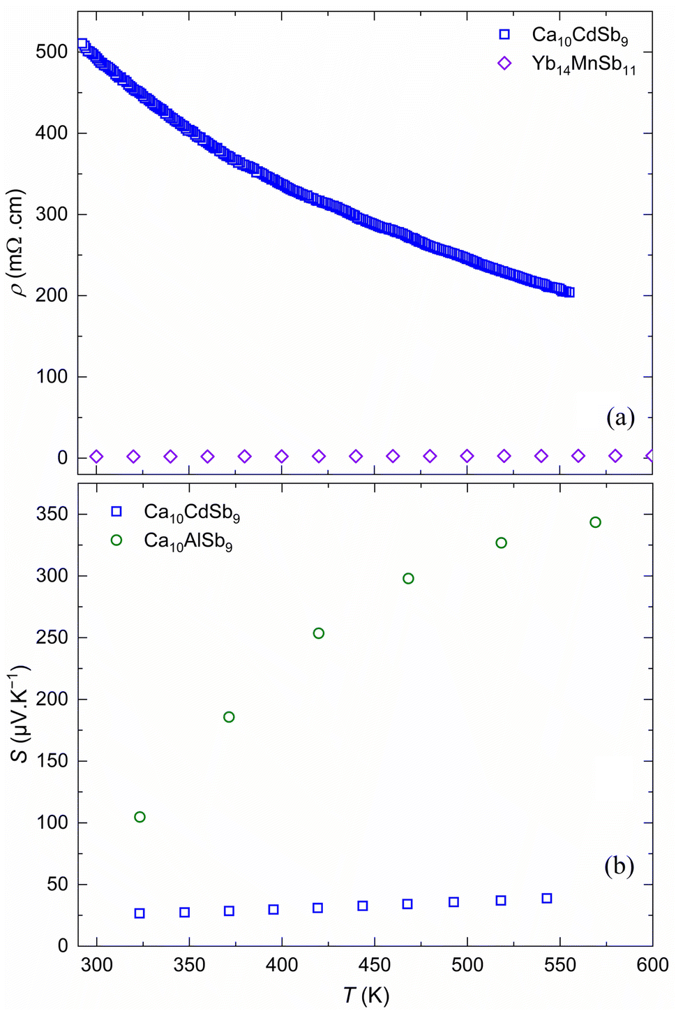 | ||
| Fig. 6 Temperature dependent (a) electrical resistivity of Ca10CdSb9 compared with that of the Yb14MnSb11 phase (a) and (b) Seebeck coefficient for sintered powder samples of Ca10MSb9 (M = Al, Cd). | ||
Ca10CdSb9 exhibits a monotonic decrease in electrical resistivity with temperature, as seen in Fig. 6a. This electrical resistivity is somewhat high for a good thermoelectric material, which can be seen here in comparison to that of the state-of-the-art Yb14MnSb11.15 However, this electrical resistivity value is lower than those of other similar materials in the family (Ca10MSb9, M = Ga, Mn, Zn).57 Similar to what was observed in these Ca10MSb9 samples with M = Ga, Mn, and Zn, there is a relatively high room temperature electrical resistivity in conjunction with a low Seebeck that is suggestive of a metallic or heavily doped semiconductor. This may indicate that there is some grain boundary scattering that could be reduced through microstructural modifications.88
Most notably, these two materials exhibit ultra-low glass-like thermal conductivity, which is of interest for thermoelectric applications. Fig. 7 shows the total thermal conductivity of these materials and compares it to those of other phases in this “10-1-9” family of materials as well as the high performing Yb14MnSb11 material.15 It can be seen that the A10MSb9 (A = Ca, Yb; M = Al, Cd, Mn, In, Ga, Zn) phases consistently exhibit very low thermal conductivities and these newly reported phases are amongst the lowest. This low thermal conductivity can be attributed to the large and complex unit cells consisting of substantial disorder, which impede phonon movement. All of these materials have thermal conductivities lower than that of the high zT material Yb14MnSb11, making them promising potential thermoelectrics. Using the measured thermal and electrical transport, the lattice thermal conductivity was calculated for the Ca10CdSb9 material. This is done using the equation κl = κtot − LσT, where κl is the lattice contribution to the thermal conductivity, κtot is the measured total thermal conductivity, L is the Lorenz number approximated using the Seebeck coefficient,89σ is the electrical conductivity, and T is the absolute temperature. However, because this material has a very high electrical resistivity and thus low electrical conductivity, the electronic contribution to the thermal conductivity, κe = LσT, is very low (on the order of 1 × 10⁻³ W m−1 K−1). This means that the lattice thermal conductivity dominates the thermal conduction in these materials and is roughly equivalent to the total thermal conductivity. This is consistent with what has been observed in other “10-1-9” compounds.54 To get the theoretical minimum lattice thermal conductivity, an intensive calculation is needed including phonon calculations, which would expand the computational scope for theoretical chemists, beyond the scope of our original goal here.
 | ||
| Fig. 7 High-temperature thermal conductivity of Ca10MSb9 (M = Al, Cd) compared with those of other reported phases with low thermal conductivity. | ||
For the Ca10CdSb9 sample, the thermoelectric power factor can be calculated via the equation PF![[double bond, length as m-dash]](https://www.rsc.org/images/entities/char_e001.gif) = S2σ, where S is the Seebeck coefficient and σ is the electrical conductivity (i.e., the inverse of the electrical resistivity, ρ). Similarly, the thermoelectric figure of merit, zT, can be calculated as follows:
= S2σ, where S is the Seebeck coefficient and σ is the electrical conductivity (i.e., the inverse of the electrical resistivity, ρ). Similarly, the thermoelectric figure of merit, zT, can be calculated as follows:
| zT = (PF)T/κ |
The calculated trends of the power factor and zT with temperature for Ca10CdSb9 are shown in Fig. 8. Despite the observed very low thermal conductivity, this material has a quite low zT due to its low power factor. The maximum zT measured here is 5 × 10⁻³, which is too low for practical thermoelectric applications. In addition to zT, the thermoelectric quality factor, B, was calculated for the Ca10CdSb9 material. The thermoelectric quality factor is calculated using the measured values for the Seebeck coefficient, electrical conductivity, and thermal conductivity90 (Fig. S5†). It provides a carrier concentration independent indication of maximum performance, with high B values corresponding to a high maximum attainable value of zT given appropriate doping. Here it can be seen that the B values are relatively low. The maximum calculated value of 3.8 × 10⁻⁴ at 520 K corresponds to a maximum possible zT of 1.5 × 10⁻³ at that temperature. However, the B increases with temperature indicating that the maximum possible zT for this material likely occurs at a higher temperature than the one measured. Additionally, the value of B is impacted by interfacial effects, so reducing the impact of grain boundaries in this material would likely increase B and thus increase the possible attainable zT.
 | ||
| Fig. 8 (a) Temperature dependence of the thermoelectric figure of merit, zT, for Ca10CdSb9. (b) Weighted mobility for Ca10CdSb9, calculated from the Seebeck coefficient and the electrical resistivity. | ||
In order to consider the dominant scattering mechanisms in this material, the weighted mobility was calculated for Ca10CdSb9, as shown in Fig. 8. The weighted mobility can be calculated from the measurements of the Seebeck coefficient and electrical resistivity and is useful in understanding underlying physics for the optimization of thermoelectric materials.91 While most materials demonstrate a decreasing trend in weighted mobility with temperature, indicating that phonon scattering dominates, here it can be seen that Ca10CdSb9 has an increasing weighted mobility with temperature. This is suggestive of grain boundary scattering like what has been observed in Mg3Sb2 samples.88 Thus, in addition to potential optimization through doping, there is also indication that the electrical resistivity could be improved by increasing the grain size in samples such as through changing the processing, allowing this material to have enhanced thermoelectric performance.
However, while this low power factor stemming from the high electrical resistivity and low Seebeck coefficient is not ideal for thermoelectric applications, this material has not been doped or otherwise further optimized. There may be routes to increase the Seebeck coefficient and/or reduce the electrical resistivity through doping with holes to enter a single carrier regime. This electronic property optimization in conjunction with the intrinsically low thermal conductivity could be a viable route to produce high quality thermoelectric materials from these two compounds. In a study conducted on the very similar Yb10MgSb9 phase, it was found that the addition of Na resulted in a significant reduction in the electrical resistivity without major reductions in the Seebeck coefficient, allowing the maximum zT to be increased from about 0.2 to greater than 1.53 Similar approaches could be considered here, where the addition of a suitable dopant would allow for an improvement of these electrical properties. Thus, while the undoped material is not a high performing thermoelectric material, the combination of the ultralow thermal conductivity and the semiconducting electronic structure with properties that can be altered through doping could allow for high performing materials through future optimization. Here, the discovery of these two new phases adds to the diverse array of AE10MSb9 (AE = Ca, Yb; M = Ga, In, Mn, Zn, Mg) materials that are worthy of further exploration to reach their full thermoelectric potential.
4. Conclusions
In this report, we presented two new Zintl antimonides with the approximate chemical formula Ca10MSb9 (M = Al and Cd), which extends the “10-1-9” family members. The new compounds exhibit a complex structure associated with high occupational and positional disorder. Both show ultralow thermal conductivity. The disorder for Ca10CdSb9 and Ca10AlSb9 is found to be different from all other “10-1-9” variants. The crystallographic disorder does not alter the (near) perfect charge balance of these phases employing the Zintl concept, which indicates semiconductor nature. The electrical resistivity of Ca10CdSb9 is relatively lower than those of other “10-1-9” members; however, its lower Seebeck coefficient limits the zT value. While Ca10AlSb9 boasts a high Seebeck coefficient, its highly reactive nature hinders accurate resistivity measurements. Both phases could be excellent starting materials for the optimization of thermoelectric properties. Currently, we are working on expanding this chemistry towards bismuthides.Data availability
CCDC numbers 2366309 and 2366310 contain the full supplementary crystallographic data for the compounds discussed in this paper.†Author contributions
Kowsik Ghosh: conceptualization, investigation, methodology, formal analysis, visualization, and writing – original draft. Leah Borgmiller: investigation, formal analysis, and writing – review & editing. Sviatoslav Baranets: conceptualization, investigation, formal analysis, and writing – review & editing. G. Jeffrey Snyder: supervision and writing – review & editing. Svilen Bobev: conceptualization, supervision, project administration, and writing – review & editing.Conflicts of interest
There are no conflicts to declare.Acknowledgements
This work was supported by the U.S. Department of Energy, Office of Science, Basic Energy Sciences, under Award # DE-SC0008885. L. B. is supported by the National Science Foundation Graduate Research Fellowship Program under Grant No. DGE-1842165. Part of this work made use of the IMSERC Crystallography facility at Northwestern University, which has received support from the Soft and Hybrid Nanotechnology Experimental (SHyNE) Resource (NSF ECCS-2025633), and Northwestern University. We sincerely thank Dr M. Ogunbunmi, who helped K. G. at the early stages of this work, and the anonymous reviewer who made very valuable suggestions with regards to the disorder modeling in Ca10CdSb9.References
- G. J. Snyder and E. S. Toberer, Nat. Mater., 2008, 7, 105–114 CrossRef CAS PubMed.
- T. C. Holgate, R. Bennett, T. Hammel, T. Caillat, S. Keyser and B. Sievers, J. Electron. Mater., 2015, 44, 1814–1821 CrossRef CAS.
- Y. Pei, A. D. Lalonde, H. Wang and G. J. Snyder, Energy Environ. Sci., 2012, 5, 7963–7969 RSC.
- A. Zevalkink, D. M. Smiadak, J. L. Blackburn, A. J. Ferguson, M. L. Chabinyc, O. Delaire, J. Wang, K. Kovnir, J. Martin, L. T. Schelhas, T. D. Sparks, S. D. Kang, M. T. Dylla, G. J. Snyder, B. R. Ortiz and E. S. Toberer, Appl. Phys. Rev., 2018, 5, 021303 Search PubMed.
- S. M. Kauzlarich, A. Zevalkink, E. Toberer and G. J. Snyder, Zintl Phases: Recent Developments in Thermoelectrics and Future Outlook, RSC Energy Environ. Ser., 2017, ch. 1, pp. 1–26 Search PubMed.
- E. S. Toberer, A. F. May and G. J. Snyder, Chem. Mater., 2010, 22, 624–634 CrossRef CAS.
- J. A. Dolyniuk, B. Owens-Baird, J. Wang, J. V. Zaikina and K. Kovnir, Mater. Sci. Eng., R, 2016, 108, 1–46 CrossRef.
- M. O. Ogunbunmi and S. Bobev, J. Mater. Chem. C, 2023, 11, 8337–8357 RSC.
- S. M. Kauzlarich, S. R. Brown and G. J. Snyder, Dalton Trans., 2007, 21, 2099–2107 RSC.
- A. Ovchinnikov and S. Bobev, J. Solid State Chem., 2019, 270, 346–359 CrossRef CAS.
- H. Kleinke, Chem. Mater., 2010, 22, 604–611 CrossRef CAS.
- B. Owens-Baird, J. Wang, S. G. Wang, Y. S. Chen, S. Lee, D. Donadio and K. Kovnir, J. Am. Chem. Soc., 2020, 142, 2031–2041 CrossRef CAS PubMed.
- A. Ovchinnikov, V. Smetana and A. V. Mudring, J. Phys.: Condens. Matter, 2020, 32, 243002 CrossRef CAS PubMed.
- R. Shang, A. He, E. L. Kunz Wille, N. H. Jo, J. C. Fettinger, P. C. Canfield and S. M. Kauzlarich, Inorg. Chem., 2023, 62, 2694–2704 CrossRef CAS PubMed.
- S. R. Brown, S. M. Kauzlarich, F. Gascoin and G. J. Snyder, Chem. Mater., 2006, 18, 1873–1877 CrossRef CAS.
- S. R. Brown, E. S. Toberer, T. Ikeda, C. A. Cox, F. Gascoin, S. M. Kauzlarich and G. J. Snyder, Chem. Mater., 2008, 20, 3412–3419 CrossRef CAS.
- E. S. Toberer, C. A. Cox, S. R. Brown, T. Ikeda, A. F. May, S. M. Kauzlarich and G. J. Snyder, Adv. Funct. Mater., 2008, 18, 2795–2800 CrossRef CAS.
- Y. Hu, J. Wang, A. Kawamura, K. Kovnir and S. M. Kauzlarich, Chem. Mater., 2015, 27, 343–351 CrossRef CAS.
- A. Zevalkink, E. S. Toberer, W. G. Zeier, E. Flage-Larsen and G. J. Snyder, Energy Environ. Sci., 2011, 4, 510–518 RSC.
- W. G. Zeier, A. Zevalkink, E. Schechtel, W. Tremel and G. J. Snyder, J. Mater. Chem., 2012, 22, 9826–9830 RSC.
- A. Zevalkink, W. G. Zeier, G. Pomrehn, E. Schechtel, W. Tremel and G. J. Snyder, Energy Environ. Sci., 2012, 5, 9121–9128 RSC.
- S. Johnsen, A. Bentien, G. K. H. Madsen and B. B. Iversen, Chem. Mater., 2006, 18, 4633–4642 CrossRef CAS.
- N. P. Blake, L. Møllnitz, G. Kresse and H. Metiu, J. Chem. Phys., 1999, 111, 3133–3144 CrossRef.
- T. Takabatake, K. Suekuni, T. Nakayama and E. Kaneshita, Rev. Mod. Phys., 2014, 86, 669–716 CrossRef CAS.
- M. Rull-Bravo, A. Moure, J. F. Fernández and M. Martín-González, RSC Adv., 2015, 5, 41653–41667 RSC.
- C. Uher and C. Semicon, Semimetals, 2001, 69, 139–253 CrossRef CAS.
- C. L. Condron, S. M. Kauzlarich, F. Gascoin and G. J. Snyder, Solid State Chem., 2006, 179, 2252–2257 CrossRef CAS.
- K. Imasato, S. D. Kang, S. Ohno and G. J. Snyder, Mater. Horiz., 2018, 5, 59–64 RSC.
- J. Zhang, L. Song, S. H. Pedersen, H. Yin, L. T. Hung and B. B. Iversen, Nat. Commun., 2017, 8, 1–8 CrossRef PubMed.
- W. Peng, S. Chanakian and A. Zevalkink, Inorg. Chem. Front., 2018, 5, 1744–1759 RSC.
- G. S. Pomrehn, A. Zevalkink, W. G. Zeier, A. Van De Walle and G. J. Snyder, Angew. Chem., Int. Ed., 2014, 53, 3422–3426 CrossRef CAS PubMed.
- F. Gascoin, S. Ottensmann, D. Stark, S. M. Haïle and G. J. Snyder, Adv. Funct. Mater., 2005, 15, 1860–1864 CrossRef CAS.
- H. Zhang, J. T. Zhao, Y. Grin, X. J. Wang, M. B. Tang, Z. Y. Man, H. H. Chen and X. X. Yang, J. Chem. Phys., 2008, 129, 164713 CrossRef PubMed.
- H. Zhang, M. Baitinger, M. B. Tang, Z. Y. Man, H. H. Chen, X. X. Yang, Y. Liu, L. Chen, Y. Grin and J. T. Zhao, Dalton Trans., 2010, 39, 1101–1104 RSC.
- K. Guo, Q. G. Cao, X. J. Feng, M. B. Tang, H. H. Chen, X. Guo, L. Chen, Y. Grin and J. T. Zhao, Eur. J. Inorg. Chem., 2011, 2011, 4043–4048 CrossRef CAS.
- X. J. Wang, M. B. Tang, H. H. Chen, X. X. Yang, J. T. Zhao, U. Burkhardt and Y. Grin, Appl. Phys. Lett., 2009, 94, 092106 CrossRef.
- A. Zevalkink, W. G. Zeier, E. Cheng, G. J. Snyder, J. P. Fleurial and S. Bux, Chem. Mater., 2014, 26, 5710–5717 CrossRef CAS.
- H. Zhang, L. Fang, M. B. Tang, Z. Y. Man, H. H. Chen, X. X. Yang, M. Baitinger, Y. Grin and J. T. Zhao, J. Chem. Phys., 2010, 133, 194701 CrossRef CAS PubMed.
- X. J. Wang, M. B. Tang, J. T. Zhao, H. H. Chen and X. X. Yang, Appl. Phys. Lett., 2007, 90, 6–9 Search PubMed.
- E. S. Toberer, A. Zevalkink, N. Crisosto and G. J. Snyder, Adv. Funct. Mater., 2010, 20, 4375–4380 CrossRef CAS.
- U. Aydemir, A. Zevalkink, A. Ormeci, H. Wang, S. Ohno, S. Bux and G. J. Snyder, Dalton Trans., 2015, 44, 6767–6774 RSC.
- A. Zevalkink, S. Chanakian, U. Aydemir, A. Ormeci, G. Pomrehn, S. Bux, J. P. Fleurial and G. J. Snyder, J. Phys.: Condens. Matter, 2015, 27, 015801 CrossRef CAS PubMed.
- S. Chanakian, A. Zevalkink, U. Aydemir, Z. M. Gibbs, G. Pomrehn, J. P. Fleurial, S. Bux and G. J. Snyder, J. Mater. Chem. A, 2015, 3, 10289–10295 RSC.
- A. Zevalkink, G. S. Pomrehn, S. Johnson, J. Swallow, Z. M. Gibbs and G. J. Snyder, Chem. Mater., 2012, 24, 2091–2098 CrossRef CAS.
- A. Zevalkink, E. S. Toberer, T. Bleith, E. Flage-Larsen and G. J. Snyder, J. Appl. Phys., 2011, 110, 013721 CrossRef.
- S. Ohno, U. Aydemir, M. Amsler, J. H. Pöhls, S. Chanakian, A. Zevalkink, M. A. White, S. K. Bux, C. Wolverton and G. J. Snyder, Adv. Funct. Mater., 2017, 27, 1–10 CrossRef.
- S. Ohno, A. Zevalkink, Y. Takagiwa, S. K. Bux and G. J. Snyder, J. Mater. Chem. A, 2014, 2, 7478–7483 RSC.
- S. K. Bux, A. Zevalkink, O. Janka, D. Uhl, S. Kauzlarich, G. J. Snyder and J. P. Fleurial, J. Mater. Chem. A, 2014, 2, 215–220 RSC.
- Y. Wang and S. Bobev, Chem. Mater., 2018, 30, 3518–3527 CrossRef CAS.
- M. O. Ogunbunmi, S. Baranets and S. Bobev, Mater. Today Adv., 2022, 16, 100310 CrossRef CAS.
- M. O. Ogunbunmi and S. Bobev, Chem. Mater., 2022, 34, 8808–8814 CrossRef CAS.
- X. Tang, B. Zhang, X. Zhang, S. Wang, X. Lu, G. Han, G. Wang and X. Zhou, ACS Appl. Mater. Interfaces, 2020, 12, 8359–8365 CrossRef CAS.
- L. Borgsmiller, Q. Li, M. Y. Toriyama and G. J. Snyder, Adv. Energy Mater., 2023, 13, 1–10 Search PubMed.
- L. Borgsmiller and G. J. Snyder, J. Mater. Chem. A, 2022, 10, 15127–15135 RSC.
- S. Baranets, A. Ovchinnikov and S. Bobev, Inorg. Chem., 2021, 60, 6702–6711 CrossRef CAS PubMed.
- L. Borgsmiller, M. Y. Toriyama and G. J. Snyder, Chem. Mater., 2024, 36, 5542–5551 CrossRef CAS.
- A. Ovchinnikov, S. Chanakian, A. Zevalkink and S. Bobev, Chem. Mater., 2021, 33, 3172–3186 CrossRef CAS.
- S. Kastbjerg, C. A. Uvarov, S. M. Kauzlarich, Y. S. Chen, E. Nishibori, M. A. Spackman and B. B. Iversen, Dalton Trans., 2012, 41, 10347–10353 RSC.
- T. Yi, C. A. Cox, E. S. Toberer, G. J. Snyder and S. M. Kauzlarich, Chem. Mater., 2010, 22, 935–941 CrossRef CAS.
- S. Bobev, V. Fritsch, J. D. Thompson, J. L. Sarrao, B. Eck, R. Dronskowski and S. M. Kauzlarich, J. Solid State Chem., 2005, 178, 1071–1079 CrossRef CAS.
- S. Q. Xia, J. Hullmann, S. Bobev, A. Ozbay, E. R. Nowak and V. Fritsch, J. Solid State Chem., 2007, 180, 2088–2094 CrossRef CAS.
- S. M. Kauzlarich, Chemistry, Structure and Bonding of Zintl Phases and Ions, Publ. by Wiley, VCH, New York, 1998 Search PubMed.
- R. Nesper, Z. Anorg. Allg. Chem., 2014, 640, 2639–2648 CrossRef CAS.
- A. D. LaLonde, T. Ikeda and G. J. Snyder, Rev. Sci. Instrum., 2011, 82, 025104 CrossRef PubMed.
- B. H. Toby, J. Appl. Crystallogr., 2001, 34, 210–213 CrossRef CAS.
- B. Eisenmann, H. Limartha, H. Schäfer and H. A. Graf, Z. Naturforsch. B, 1980, 35, 1518–1524 CrossRef.
- SAINT, Bruker AXS Inc., Madison, WI, USA, 2014 Search PubMed.
- SADABS, Bruker AXS Inc., Madison, WI, USA, 2014 Search PubMed.
- G. M. Sheldrick, Acta Crystallogr., Sect. A, 2015, 71, 3–8 CrossRef PubMed.
- G. M. Sheldrick, Acta Crystallogr., Sect. C: Struct. Chem., 2015, 71, 3–8 Search PubMed.
- O. K. Andersen, Phys. Rev. B: Solid State, 1975, 12, 3060–3083 CrossRef CAS.
- O. K. Andersen and O. Jepsen, Phys. Rev. Lett., 1984, 53, 2571–2574 CrossRef CAS.
- U. Von Barth and L. A. Hedin, J. Phys. C: Solid State Phys., 1972, 5, 1629–1642 CrossRef CAS.
- S. Steinberg and R. Dronskowski, Crystals, 2018, 8, 225 CrossRef.
- K. A. Borup, E. S. Toberer, L. D. Zoltan, G. Nakatsukasa, M. Errico, J. P. Fleurial, B. B. Iversen and G. J. Snyder, Rev. Sci. Instrum., 2012, 83, 123902 CrossRef PubMed.
- S. Iwanaga, E. S. Toberer, A. LaLonde and G. J. Snyder, Rev. Sci. Instrum., 2011, 82, 063905 CrossRef PubMed.
- S. Baranets and S. Bobev, J. Am. Chem. Soc., 2021, 143, 65 CrossRef CAS PubMed.
- K. Deller and B. Eisenmann, Z. Naturforsch. B, 1975, 31, 29–34 CrossRef.
- E. A. Leon-Escamilla, W. M. Hurng, E. S. Peterson and J. D. Corbett, Inorg. Chem., 1997, 36, 703–710 CrossRef CAS.
- A. K. Ganguli, S. Gupta and J. D. Corbett, Inorg. Chem., 2006, 45, 196–200 CrossRef CAS PubMed.
- L. Borgsmiller, M. Y. Toriyama, H. E. Kurtz, T. Ha, A. Al Rumaih and G. J. Snyder, Chem. Mater., 2024, 35, 10150–10155 CrossRef.
- K. Ghosh and S. Bobev, Solids, 2023, 4, 344–355 CrossRef CAS.
- A. Ovchinnikov, G. M. Darone, B. Saparov and S. Bobev, Materials, 2018, 11, 1–13 CrossRef PubMed.
- A. B. Childs, S. Baranets and S. Bobev, J. Solid State Chem., 2019, 278, 120889 CrossRef CAS.
- A. Balvanz, S. Baranets and S. Bobev, J. Solid State Chem., 2020, 289, 121476 CrossRef CAS.
- E. S. Toberer, S. R. Brown, T. Ikeda and S. M. Kauzlarich, Appl. Phys. Lett., 2008, 93, 11–14 CrossRef.
- C. J. Perez, M. Wood, F. Ricci, G. Yu, T. Vo, S. K. Bux, G. Hautier, G. M. Rignanese, G. J. Snyder and S. M. Kauzlarich, Sci. Adv., 2021, 7, 1–9 Search PubMed.
- J. J. Kuo, S. D. Kang, K. Imasato, H. Tamaki, S. Ohno, T. Kanno and G. J. Snyder, Energy Environ. Sci., 2018, 11, 429–434 RSC.
- H. S. Kim, Z. M. Gibbs, Y. Tang, H. Wang and G. J. Snyder, APL Mater., 2015, 3, 041506 CrossRef.
- S. D. Kang, and G. J. Snyder, Advances in Thermoelectricity: Foundational Issues, Materials and Nanotechnology, 2021, vol. 107, pp. 27–36 Search PubMed.
- G. J. Snyder, A. H. Snyder, M. Wood, R. Gurunathan, B. H. Snyder and C. Niu, Adv. Mater., 2020, 32, 2001537 CrossRef CAS PubMed.
Footnote |
| † Electronic supplementary information (ESI) available. CCDC 2366309 and 2366310. For ESI and crystallographic data in CIF or other electronic format see DOI: https://doi.org/10.1039/d4ta05000b |
| This journal is © The Royal Society of Chemistry 2024 |