
 Open Access Article
 This Open Access Article is licensed under a
 Creative Commons Attribution 3.0 Unported Licence
Effect of different halide-based ligands on the passivation and charge carrier dynamics in AgBiS2 nanocrystal solar cells†
Fiona
Treber
 a,
Elke
De Grande
a,
Ute B.
Cappel
bc and
Erik M. J.
Johansson
*a
a,
Elke
De Grande
a,
Ute B.
Cappel
bc and
Erik M. J.
Johansson
*a
aDepartment of Chemistry-Ångström, Physical Chemistry, Uppsala University, 75120 Uppsala, Sweden. E-mail: erik.johansson@kemi.uu.se
bCondensed Matter Physics of Energy Materials, Division of X-ray Photon Science, Department of Physics and Astronomy, Uppsala University, Box 516, 75120 Uppsala, Sweden
cWallenberg Initiative Materials Science for Sustainability, Department of Physics and Astronomy, Uppsala University, 75120 Uppsala, Sweden
First published on 23rd October 2024
Abstract
AgBiS2 nanocrystals have been shown to be a promising material for solar cell applications due to their high absorption coefficient, solution-processability and stability. However, detailed and systematic insight into how different surface passivation agents affect the overall material properties and corresponding device performance is still limited. Herein, a study about AgBiS2 nanocrystals treated with five different halide-based compounds – TBAI, TMAI, TBABr, TMABr and TMACl – is presented, with the nanocrystals themselves being synthesised via a newly adapted route under atmospheric conditions. For the differently passivated samples, variation in the ligand uptake, as well as shifts in the position of the valence and conduction bands could be observed. Incorporating these ligand-treated thin films into solar cell devices allowed for further investigation of their overall performance as well as into their respective charge carrier dynamics. Markedly longer charge carrier lifetimes were observed for the bromide- and chloride-passivated samples through transient photovoltage and photocurrent measurements as well as impedance spectroscopy. The effect of the surface modification on the charge carrier transport behaviour, on the other hand, was found to be less pronounced. Overall, this work demonstrates the importance of better understanding how different ligands affect nanocrystal properties, showcasing how it influences a wide variety of parameters controlling final device performance.
1 Introduction
Due to their unique properties, nano-crystalline materials attract considerable attention regarding their potential utilisation in a wide range of applications.1 For optoelectronic devices and solar cells in particular, the tunability of the material's band gap via particle size variation offers a significant advantage, while the normally colloidal nature of the nanocrystals (NCs) provides the opportunity for low-cost solution-based processing.2,3 Consequently, different materials were investigated to that effect, with one of the most prominent and well-studied examples being PbS, which resulted in certified power conversion efficiencies (PCEs) exceeding 11%.4,5 However, concerns regarding the toxicity of lead motivated a search for more environmentally benign alternatives. The ternary metal chalcogenide compound AgBiS2 was identified as a promising candidate in that regard by Bernechea et al. in 2016.6 Besides exhibiting a high absorption coefficient of around 105 cm−1 and having a suitable band gap ranging between 1.0 eV and 1.3 eV for typical particle sizes below 10 nm, this material was also shown to provide good chemical stability under ambient conditions.6–8 Many previous studies so far have focused on the optimisation of the solar cell performance by improving the AgBiS2 NCs themselves through various synthesis and processing conditions, or by employing device engineering, mostly by tuning the adjacent hole and electron transport layers.7,9–13 While these efforts yielded very good results in terms of improved device efficiencies,14 there are still a lot of areas, where further fundamental knowledge and understanding is needed. One such area is the complex interplay between the AgBiS2 NCs and their surface-terminating ligands. This topic is especially important to address, since it has previously been shown for other nano-crystalline compounds that the choice in passivating ligand can affect a wide variety of material properties, including recombination rates, the doping profile, as well as the positions of the valence (VB) and conduction bands (CB).5,15–17 Besides this, ligands play a significant role in the charge transport throughout the corresponding NC film, which is important in any kind of optoelectronic device.1,17,18 As a consequence, typical NC solar cell fabrication includes a ligand exchange step, which replaces the native insulating long chain aliphatic ligands, like oleic acid (OA) and oleylamine (OLAm), commonly used for colloidal synthesis and long term storage with smaller electrically better conducting ones.3,7,17,19 Previously published data utilizing different ligands during this exchange, such as tetramethylammonium iodide (TMAI), ethanedithiol (EDT), ethanethiol (ET) and 3-mercaptopropionic acid (3-MPA), indicates that the described effects also play a role in AgBiS2 NC-based solar cells.6,9,14,20 However, not much work has been done with the aim of comparing these differences in-depth and for multiple ligands at once yet, considering that the aforementioned data mainly stems from separate studies that have their focus elsewhere.Therefore, this study aims to improve on the knowledge regarding AgBiS2–ligand interaction in thin films in general and its consequences and effects on the solar cell performance in particular, while pursuing a fully ambient synthesis and fabrication process. The ligands tested via solid-state ligand exchange (SSLE) for that purpose are salts containing either tetrabutylammonium (TBA) and tetramethylammonium (TMA) cations, with either iodide (I), bromide (Br) or chloride (Cl) as the respective anions. In total, the five different compounds used were TBAI, TMAI, TBABr, TMABr and TMACl. This approach allowed for the investigation into different anion and cation sizes, as well as the respective affinities of the halides towards AgBiS2. We found that the passivation-effect can be mainly ascribed to the halides, with their respective uptake decreasing significantly from I to its smaller analogues Br and Cl. In addition to the effect the different ligand incorporation had on the energy levels of the VB and CB, this led to differences in solar cell performance as well. Special attention was paid to the effect the passivation had on the recombination and charge transport in the respective solar cell devices. To investigate that in detail, transient photocurrent and photovoltage techniques were paired with impedance spectroscopy to gain further insights. Interestingly, it was found that even though the ligand uptake was less for the smaller halides, the resulting devices showed significantly improved charge carrier lifetimes.
2 Results and discussion
For the fabrication of the AgBiS2 NCs, concepts from different known synthesis routes were taken and combined to allow for particle formation without the need for an inert atmosphere, while avoiding in situ passivation by ligands that would prove to be difficult to exchange later on. A simplified scheme of the procedure can be seen in Fig. 1(a), while a more detailed description is provided under Methods in Section 4. In short, elemental sulphur dissolved in OLAm at room temperature (RT) is used as a precursor to circumvent the necessity of using inert gas techniques required to handle organo-sulphur compounds commonly used in hot injection methods.21 This is in agreement with the previously published method by Akgul et al. for synthesising AgBiS2 NCs under ambient conditions.9 However, full adaptation of that process proved unsuitable for this study, due to the presence of 1-octanethiol during the synthesis, which could not be exchanged for halide-based ligands later on. Additionally, the use of silver and bismuth halide salts as precursors as reported could lead to in situ passivation of the formed NCs by the specific halide as reported previously for PbS, which in turn would distort the results of the planned halide-based SSLE.22 Therefore, silver and bismuth acetates (AgOAc and BiOAc3) were used instead, similar to the standard hot injection method.6,23 These metal precursors were first separately dissolved in toluene with the help of OLAm and OA, respectively, before combining them, inspired by the results published by Hu et al.13 Then, the mixture was held at 100 °C for the injection of the sulphur precursor, after which the crude NC dispersion was left to cool down to RT before purifying it through repeated precipitation with acetone. The final product redispersed in toluene had a dark brown colour and was stable under ambient conditions for months. To analyse the synthesised material, X-ray diffraction (XRD) was carried out on the drop cast NCs in a grazing incident geometry. The obtained diffractogram is depicted in Fig. 1(b) and it shows the expected peak broadening of a nanocrystalline sample. Upon comparison with previously published crystallographic data, it is confirmed that the correct cubic rock salt like crystal structure with space group Fm![[3 with combining macron]](https://www.rsc.org/images/entities/char_0033_0304.gif) m has been formed.24 The absorption spectrum of the diluted colloidal dispersion (Fig. 1(c)), on the other hand, is characterised by a featureless increase towards smaller wavelengths. Further analysis in form of a Tauc plot revealed an indirect band gap (BG) of about 1.14 eV, again being in good agreement with previous findings for AgBiS2 NCs.6,7 To verify the nanocristallinity and gain insights into the morphology and size distribution of the prepared sample, transmission electron microscopy (TEM) was utilised to obtain images of the synthesised particles. As can be seen in Fig. 1(d), the NCs appear to be mostly spherical in shape and their average size was found to be 5.1 nm in diameter, with values ranging between 2.5 nm and 8.9 nm. Additional images to showcase the overall homogeneity of the prepared particles together with a more detailed histogram representing the size distribution measured in these images are presented in Fig. S1 in the ESI.†
m has been formed.24 The absorption spectrum of the diluted colloidal dispersion (Fig. 1(c)), on the other hand, is characterised by a featureless increase towards smaller wavelengths. Further analysis in form of a Tauc plot revealed an indirect band gap (BG) of about 1.14 eV, again being in good agreement with previous findings for AgBiS2 NCs.6,7 To verify the nanocristallinity and gain insights into the morphology and size distribution of the prepared sample, transmission electron microscopy (TEM) was utilised to obtain images of the synthesised particles. As can be seen in Fig. 1(d), the NCs appear to be mostly spherical in shape and their average size was found to be 5.1 nm in diameter, with values ranging between 2.5 nm and 8.9 nm. Additional images to showcase the overall homogeneity of the prepared particles together with a more detailed histogram representing the size distribution measured in these images are presented in Fig. S1 in the ESI.†
 | ||
| Fig. 1 AgBiS2 synthesis and material characterisation: (a) synthesis scheme, (b) XRD data and ref. 24, (c) absorbance spectra with Tauc plot as inset and (d) TEM image of as-synthesised NCs. | ||
To also account for the elemental composition of the NCs synthesised with the described adapted method, X-ray photoelectron spectroscopy (XPS) was employed. The measurements were carried out on the five ligand-exchanged thin films, though, to simultaneously study the respective ligand uptake, as well as investigating potential changes to the constituents caused by the SSLE. The results obtained for the relevant core-level signals are depicted in Fig. 2, while the respective survey spectra of the ligand-exchanged thin films, in addition to data from an as-synthesised sample, are presented in Fig. S2 in the ESI.† Overall, they do not show any other impurities besides the expected signals for oxygen and carbon. When considering the ratio between the signals from the NC-related constituents and the impurities, however, a clear difference between the films having undergone SSLE and the untreated one can be observed (compare Fig. S2 and Table S1, ESI†). The former show a pronounced reduction in the carbon and oxygen signals, indicating a significant removal of the overall synthesis ligands. Additionally, it is interesting to note that no signal from nitrogen could be picked up, implying a rather complete removal of the OLAm, as one of the synthesis ligands. Moreover, the absence of a nitrogen signal further suggests no significant incorporation of either TBA or TMA took place during the SSLE. The corresponding elemental ratios calculated from the XPS spectra for the five different samples are listed in Table 1. Generally, all NC films seem to incorporate a lower amount of sulphur than indicated by the stoichiometric ratios of the corresponding bulk material AgBiS2. This characteristic is in agreement with previous reports, since metal chalcogenide NCs tend to have metal-rich surfaces.6,25,26 Regarding the silver to bismuth ratio, which has previously been shown to be an important determining factor in the material's properties especially in solar cell applications, the obtained results indicate a slightly silver rich composition of the prepared NCs.6,7 There is a notable trend though with the difference in relative amounts between the two metal components seemingly decreasing slightly for the smaller ligands. Another more pronounced trend visible is the considerably lower uptake in Br and Cl, compared to I during the ligand exchange. This could potentially be explained by the high affinity between silver and iodide, as predicted by the hard and soft acids and bases (HSAB) concept, which classifies both of these ions as a soft Lewis acid and base, respectively.27 Additionally, the presented data here implies that the halide incorporation into the AgBiS2 surface seems to get slightly enhanced by the smaller TMA cation in case of both I and Br. Generally, these findings indicate a significant difference in surface structure of the NCs depending on the specific ligand they were treated with, irrespective of their chemical similarity. Taking a closer look at the core-level signals though, it becomes apparent that the Ag 3d signal (Fig. 2(a)) unexpectedly does not seem to be changing depending on the ligand treatment. In all cases, the Ag 3d5/2 peak is centred around 367.9 eV and can be fitted with only one component, while the spin orbit splitting is constant at 6.0 eV.6,7 However, before taking these results as a verification that silver is not affected at all by the change in surface structure and makeup depending on the ligand treatment, one needs to consider that the expected differences in binding energies between electrons ejected from silver bound to sulphur or the halides in question is very small.6,28 This even extends to other elements, like oxygen, which could instead be present on the NCs surfaces, especially if the passivation by the halides is not sufficient, leaving room for potential oxidation due to the ambient processing.28 The Bi 4f signal presented in Fig. 2(b), on the other hand, shows clear signs of change between the five ligands. In each case, it is made up of a low and high binding energy component with the corresponding two 4f7/2 peaks centred around 158.1 eV and 158.8 eV, respectively, similar to previous observations of this material passivated with TMAI or TBAI.6,7 However, whereas for both TBAI and TMAI, the relative areas of both components are close to 1![[thin space (1/6-em)]](https://www.rsc.org/images/entities/char_2009.gif) :1, for the smaller ligands TBABr, TMABr and TMACl, the high energy component increases, while the low energy one simultaneously decreases. As a result, the ratio between them becomes closer to 1:2, with the high energy component dominating. Previously, the high energy component has been assigned to both Bi–S and Bi–I bonds in TMAI passivated AgBiS2 NCs, while the low energy component has been associated with a type of Bi–S bond that allows the bismuth to retain a lot of its electron density, which in turn has been correlated to higher trap densities.6,29 Here, it is additionally proposed that the high energy component at 158.8 eV represents a partially oxidised Bi–S species, since its increase coincides with a significantly lower amount of halide ligands on the surface of the NCs, making a full passivation prohibiting oxidisation unlikely. This assumption is further supported by a relative increase in the amount of oxygen detected in these samples (compare Table S1, ESI†). The remaining 2 peaks at 161.0 eV and 162.2 eV visible in Fig. 2(b) can be assigned to S 2p.7 However, any in-depth analysis of this signal is impeded by the overlap with the much more intense Bi 4f response. Therefore, the S 2s signal was also recorded and is presented in Fig. 2(c). From that, it can be observed that there are three components in total. The one at low binding energies around 225.3 eV can be assigned to the S–Ag and S–Bi bonds, while the second one has its maximum between 227.0 eV and 227.5 eV, depending on the ligand.9,30 These binding energies are slightly below what is expected for elemental sulphur, but higher than normal S–metal bonds, therefore either indicating some degree of incomplete reduction during the synthesis or a partial re-oxidisation at some later point. The last component centred around 231.8 eV, though, can clearly be assigned to some form of S–O species, probably formed at the surface.30 Again, while this signal is present in all five cases presented here, a clear difference can be seen between the bromide- and chloride-based ligands, compared to TBAI and TMAI. Whereas for the latter, this signal is comparatively small, it increases significantly with the decreased halide uptake in case of Br and Cl. This might imply that even though none of the halides are expected to passivate the S-sites directly, the higher amount of iodide present at neighbouring Ag- or Bi-sites and its larger size may also partially inhibit sulphur oxidisation due to steric hindering. Lastly, the different ligand signals themselves are presented in Fig. 2(d). From TBAI and TMAI, the resulting I 3d3/2 peaks can be observed at 619.0 eV, with a spin orbit splitting of 11.5 eV in both cases.7 Opposed to that, the spin orbit splitting for the Br 3d from TBABr and TMABr was found to be roughly 1.1 eV, which results in a significant overlap between both peaks with maxima at 68.0 ev and 69.1 eV.31 Similarly, the two peaks from the Cl 2p signal overlap as well due to a spin orbit splitting of around 1.6 eV, with the Cl 2p3/2 maximum being located at 197.8 eV.28,31 Overall, the XPS findings further confirm that the adapted synthesis method provides the desired material, while there seems to be significant differences in surface composition of the NCs between iodide-based ligands and its smaller halogen analogous, where oxides are expected to play an additional but crucial role in the passivation and charge neutrality. Nevertheless, ligand exchange in general seems to be taking place in all cases and layer-by-layer film formation is achievable for all ligands.
:1, for the smaller ligands TBABr, TMABr and TMACl, the high energy component increases, while the low energy one simultaneously decreases. As a result, the ratio between them becomes closer to 1:2, with the high energy component dominating. Previously, the high energy component has been assigned to both Bi–S and Bi–I bonds in TMAI passivated AgBiS2 NCs, while the low energy component has been associated with a type of Bi–S bond that allows the bismuth to retain a lot of its electron density, which in turn has been correlated to higher trap densities.6,29 Here, it is additionally proposed that the high energy component at 158.8 eV represents a partially oxidised Bi–S species, since its increase coincides with a significantly lower amount of halide ligands on the surface of the NCs, making a full passivation prohibiting oxidisation unlikely. This assumption is further supported by a relative increase in the amount of oxygen detected in these samples (compare Table S1, ESI†). The remaining 2 peaks at 161.0 eV and 162.2 eV visible in Fig. 2(b) can be assigned to S 2p.7 However, any in-depth analysis of this signal is impeded by the overlap with the much more intense Bi 4f response. Therefore, the S 2s signal was also recorded and is presented in Fig. 2(c). From that, it can be observed that there are three components in total. The one at low binding energies around 225.3 eV can be assigned to the S–Ag and S–Bi bonds, while the second one has its maximum between 227.0 eV and 227.5 eV, depending on the ligand.9,30 These binding energies are slightly below what is expected for elemental sulphur, but higher than normal S–metal bonds, therefore either indicating some degree of incomplete reduction during the synthesis or a partial re-oxidisation at some later point. The last component centred around 231.8 eV, though, can clearly be assigned to some form of S–O species, probably formed at the surface.30 Again, while this signal is present in all five cases presented here, a clear difference can be seen between the bromide- and chloride-based ligands, compared to TBAI and TMAI. Whereas for the latter, this signal is comparatively small, it increases significantly with the decreased halide uptake in case of Br and Cl. This might imply that even though none of the halides are expected to passivate the S-sites directly, the higher amount of iodide present at neighbouring Ag- or Bi-sites and its larger size may also partially inhibit sulphur oxidisation due to steric hindering. Lastly, the different ligand signals themselves are presented in Fig. 2(d). From TBAI and TMAI, the resulting I 3d3/2 peaks can be observed at 619.0 eV, with a spin orbit splitting of 11.5 eV in both cases.7 Opposed to that, the spin orbit splitting for the Br 3d from TBABr and TMABr was found to be roughly 1.1 eV, which results in a significant overlap between both peaks with maxima at 68.0 ev and 69.1 eV.31 Similarly, the two peaks from the Cl 2p signal overlap as well due to a spin orbit splitting of around 1.6 eV, with the Cl 2p3/2 maximum being located at 197.8 eV.28,31 Overall, the XPS findings further confirm that the adapted synthesis method provides the desired material, while there seems to be significant differences in surface composition of the NCs between iodide-based ligands and its smaller halogen analogous, where oxides are expected to play an additional but crucial role in the passivation and charge neutrality. Nevertheless, ligand exchange in general seems to be taking place in all cases and layer-by-layer film formation is achievable for all ligands.
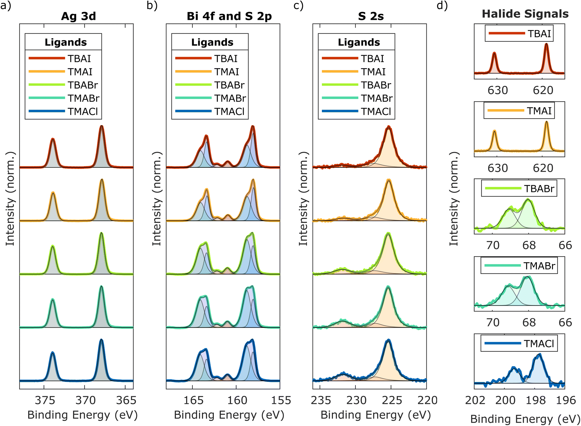 | ||
| Fig. 2 XPS core level spectra of AgBiS2 thin films treated with different ligands: (a) Ag 3d signal, fitted with one component, (b) overlapping Bi 4f and S 2p signals, fitted with 2 components for the Bi 4f (blue/green areas) and 1 component for the S 2p signals (red/orange areas), (c) S 2s signal, fitted with 3 components and (d) the different halide signals (I 3d, Br 3d, Cl 2p), fitted with one component each. | ||
| TBAI | TMAI | TBABr | TMABr | TMACl | |
|---|---|---|---|---|---|
| Ag (%) | 30.7 | 30.8 | 31.2 | 30.7 | 30.2 |
| Bi (%) | 25.8 | 26.3 | 27.3 | 28.2 | 27.4 |
| S (%) | 37.0 | 35.8 | 40.2 | 39.7 | 41.3 |
| Ligand (%) | 6.6 | 7.1 | 1.3 | 1.5 | 1.2 |
2.1 Devices and characterisation
To test the effect these differences have on the device performance, solar cells with an architecture according to Fig. 3(a) were fabricated with the AgBiS2 NCs in the active layer passivated by either TBAI, TMAI, TBABr, TMABr or TMACl. An exemplary scanning electron microscopy (SEM) cross-section image of one of the devices can be seen in Fig. 3(b), while the other ones regarding the remaining fours samples are depicted in Fig. S3 in the ESI.† In short, ITO covered glass was used as the transparent front contact, followed by zinc oxide (ZnO) to achieve electron selectivity with it functioning as the electron transport, respectively hole blocking, layer (ETL/HBL). The active layer containing the differently passivated AgBiS2 NCs was fabricated by SSLE in a layer-by-layer deposition method. To keep the presented samples comparable, all devices were made with three layers of the NCs, without any further optimisation to boost absorbance and thereby increase charge carrier generation for the distinct NC–ligand combinations. For the hole transport/electron blocking layer (HTL/EBL), poly(3-hexylthiophene-2,5-diyl) (P3HT) was applied on top of the AgBiS2 NCs, before MoO3 and silver were evaporated onto the structure to form the back contact. P3HT was chosen here due to its compatibility with ambient processing and storage under dry air conditions. Furthermore, it has been shown to provide good robustness and reproducibility, which is the main priority of this study to enable and facilitate the desired comparative focus of this work.7 Additionally, and to the same effect, the layer thickness of the P3HT was reduced compared to the previously employed recipe by utilizing dynamic instead of static coating to limit the otherwise significant influence of the co-absorption by the HTL. Consequently, the power conversion efficiencies (PCEs) are expected to be lower than previously reported values. Looking at the results from the JV characteristics of the best performing samples of each ligand presented in Fig. 3(c) and summarised in Table 2, this is confirmed. Nevertheless, all solar cells provide decent efficiencies with no apparent hysteresis behaviour (see Fig. S4 in ESI†), independent of the passivating material. Even though the differences in PCE regarding the chosen ligands are moderate, there are some interesting trends to be observed. While the three devices with NCs passivated by either Br or Cl show a generally higher VOC and slightly improved FF, the ones featuring I on the AgBiS2 surface instead seem to provide a better JSC. The former observation coincides with the findings from the XPS characterisation of the thin films, where it was found that SSLE treatment with the smaller halide ligands lead to a decreased low energy bismuth signal (compare Fig. 2(b)), commonly associated with anomalous defect-inducing Bi–S bonding.6,29 Therefore, the higher VOC might be attributed to a better passivation of trap states in these devices. Moreover, this behaviour was not only found for the best devices, but rather a general trend also reflected in the respective box plots provided in Fig. S5 in the ESI,† where ten equally fabricated samples for each ligand from different batches are considered. To be able to explain the differences in JSC caused by the changed passivation, a more detailed analysis of the active layer's response to illumination is needed. Thus, the incident photon-to-current conversion efficiency (IPCE) of the five best performing devices from Fig. 3(c) were measured over the visible and into the near-infrared spectrum to evaluate potential differences between the samples. The obtained curves are presented in Fig. 3(d) and show qualitatively the same features and overall trends. However, there are clear quantitative differences, with a steady increase in IPCE over most wavelengths from the smallest (TMACl) to the largest (TBAI) ligand compound. Consequently, the integrated JSC from the IPCE curves (see Table S2, ESI†) reflect the same trend and similar values compared to the ones from the JV data. Since this is not yet indicative of the cause for the observed differences, absorbance spectra of the halide-passivated AgBiS2 thin films are used to compare whether this trend seems to be related to changes in the charge transport and extraction or if already the absorbance profile and consequently the charge carrier generation is affected by the choice in ligand. As can be observed in Fig. 3(e), these absorbance spectra exhibit the same trends regarding their relative intensities as the IPCE curves in Fig. 3(d), thereby indicating that a significant amount of the differences in JSC can be attributed to a weaker absorption of the films made with the smaller halides. Taking into consideration the data displayed in Fig. 3(f), where the resulting average layer thicknesses (see Fig. 3(b) and S3, ESI†) of the five NC films are shown, a main contributor for the difference in absorbance and subsequent charge carrier generation apparently is the change in thickness of the photoactive layer as a result of the ligand treatment. Furthermore, the variation in the AgBiS2 layer thickness per type of sample, represented by the error bars in Fig. 3(f), seems to be closely correlated to the spread in JSC and subsequently PCE regarding solar cells of identical fabrication conditions observable in the corresponding box plot of these device parameters in Fig. S5 in the ESI.† To further investigate these aspects, illumination dependent JV measurements were carried out. Plotting the obtained JSC values against light intensity I and fitting the data points with the power-law expression, JSC ∝ Iα, as is done in Fig. 3(g), allows for the extraction of the power factor α, which is a measure of the charge extraction in a given device. While α = 1 represents the ideal case of full charge extraction, any deviation below unity signifies incomplete extraction of charge carriers before recombination.20 The obtained values for α for the five investigated samples are listed in Table 3. Even though there are losses present in all samples, overall the charge extraction seems to be working well for all tested ligands. However, under closer inspection there are some subtle trends to be made out. First, comparing the results gained from ligand salts with the same cations, it becomes apparent that in both cases α decreases slightly for decreasing halide anion size (αTMAI > αTMABr > αTMACl and αTBAI > αTBABr). On the other hand, treatment with compounds having TMA as the cation apparently lead to better charge extraction than those treated with TBA containing salts (αTMAI > αTBAI and αTMABr > αTBABr). Additionally, the ideality factor nid can be determined from the same illumination dependent JV measurements, by plotting the VOC instead of the JSC against the light intensity, as is shown in Fig. 3(h). Fitting the data points and further calculations according to yields the desired values, which are also presented in Table 3. The ideality factor is commonly related to the recombination mechanism dominating a given device, with nid = 1 describing the ideal case where only band-to-band recombination occurs. Values above 1, on the other hand, indicate that additional recombination pathways, such as trap-assisted Shockley–Read–Hall (SRH) recombination (nid = 2), are also present.20 Besides this, it has been shown that more complex mechanisms, such as ones related to surface recombination, can lead to values outside of the described interval.32 Here, all five tested devices exhibit ideality factors between 1 and 2, indicating that multiple recombination pathways exist for each of them. However, there are apparent differences based on the ligands employed, with the I-passivated NCs showing significantly higher values, than the ones treated with Br or Cl. This fits in well with the previous observations about the smaller halides providing a higher VOC overall and the proposed connection to the reduced anomalous trap-related Bi–S bonding in these materials. Besides this, additional trap-states at the interface between the AgBiS2 layer and the adjacent ETL and HTL could also contribute to the these observations regarding the ideality
factor, since changes in NC passivation are able to shift the position of the VB an CB, as well as effect the Fermi level EF.5 Hence, the interface formation might also be affected by the different ligands. To gain some insights into these phenomena, ultra-violet photon spectroscopy (UPS) was utilised to obtain the position of the VB edge against the Fermi level and the work function of the sample surface. The measured spectra with the relevant fits are presented in Fig. S6 in the ESI,† while the extracted corresponding values for the work function and VB edge are listed in Table S3, ESI.† In order to get a full picture also including the CB edge, these results are combined with the optical BGs obtained from both the Tauc plots of the thin film absorbance measurements as well as from the IPCE spectra (see Fig. S7, ESI†). Interestingly, the values obtained from the thin films with 1.2 eV were slightly higher than the band gap estimated for the NCs in dispersion as displayed in Fig. 1(c). According to the resulting data depicted in Fig. 3(i), all NC samples show rather intrinsic behaviour as previously seen for TMAI.6 Besides that, the respective energy levels change depending on the ligand used for surface treatment, with a shift towards lower energies taking place from TBAI over TMAI to TBABr. Afterwards, a slight shift back towards higher energies can be observed for TMABr and TMACl. Generally though, the Br- and Cl-based ligands seem to result in a slightly lower lying VB, EF and CB than their I-based analogues.
yields the desired values, which are also presented in Table 3. The ideality factor is commonly related to the recombination mechanism dominating a given device, with nid = 1 describing the ideal case where only band-to-band recombination occurs. Values above 1, on the other hand, indicate that additional recombination pathways, such as trap-assisted Shockley–Read–Hall (SRH) recombination (nid = 2), are also present.20 Besides this, it has been shown that more complex mechanisms, such as ones related to surface recombination, can lead to values outside of the described interval.32 Here, all five tested devices exhibit ideality factors between 1 and 2, indicating that multiple recombination pathways exist for each of them. However, there are apparent differences based on the ligands employed, with the I-passivated NCs showing significantly higher values, than the ones treated with Br or Cl. This fits in well with the previous observations about the smaller halides providing a higher VOC overall and the proposed connection to the reduced anomalous trap-related Bi–S bonding in these materials. Besides this, additional trap-states at the interface between the AgBiS2 layer and the adjacent ETL and HTL could also contribute to the these observations regarding the ideality
factor, since changes in NC passivation are able to shift the position of the VB an CB, as well as effect the Fermi level EF.5 Hence, the interface formation might also be affected by the different ligands. To gain some insights into these phenomena, ultra-violet photon spectroscopy (UPS) was utilised to obtain the position of the VB edge against the Fermi level and the work function of the sample surface. The measured spectra with the relevant fits are presented in Fig. S6 in the ESI,† while the extracted corresponding values for the work function and VB edge are listed in Table S3, ESI.† In order to get a full picture also including the CB edge, these results are combined with the optical BGs obtained from both the Tauc plots of the thin film absorbance measurements as well as from the IPCE spectra (see Fig. S7, ESI†). Interestingly, the values obtained from the thin films with 1.2 eV were slightly higher than the band gap estimated for the NCs in dispersion as displayed in Fig. 1(c). According to the resulting data depicted in Fig. 3(i), all NC samples show rather intrinsic behaviour as previously seen for TMAI.6 Besides that, the respective energy levels change depending on the ligand used for surface treatment, with a shift towards lower energies taking place from TBAI over TMAI to TBABr. Afterwards, a slight shift back towards higher energies can be observed for TMABr and TMACl. Generally though, the Br- and Cl-based ligands seem to result in a slightly lower lying VB, EF and CB than their I-based analogues.
 | ||
| Fig. 3 Basic solar cell structure, characterisation and related thin film results: (a) schematic structure of the solar cell architecture (not to scale), (b) corresponding SEM cross-section of a TMAI-passivated device, (c) JV-characteristics of the different samples, with the corresponding IPCE results in (d) and (e) relative absorbance profiles of the AgBiS2 thin films, (f) active layer thicknesses extracted from the SEM cross-section images ((b) and Fig. S3, ESI;† 30 measurements each), (g) illumination dependent JSC, (h) illumination dependent VOC and (i) energy levels of the differently passivated AgBiS2 NC thin films, extracted from UPS measurements together with the band gap values established via absorbance spectroscopy. | ||
| V OC (V) | J SC (mA cm−2) | FF (%) | PCE (%) | |
|---|---|---|---|---|
| TBAI | 0.34 | −13.40 | 51.18 | 2.30 |
| TMAI | 0.34 | −12.16 | 47.72 | 1.96 |
| TBABr | 0.38 | −11.13 | 53.29 | 2.24 |
| TMABr | 0.41 | −11.01 | 54.29 | 2.43 |
| TMACl | 0.36 | −10.68 | 54.68 | 2.21 |
| TBAI | TMAI | TBABr | TMABr | TMACl | |
|---|---|---|---|---|---|
| α | 0.92 | 0.96 | 0.87 | 0.95 | 0.89 |
| n id | 1.65 | 2.01 | 1.42 | 1.54 | 1.41 |
2.2 Charge carrier dynamics
So far, only steady-state characterisations of the solar cells have been discussed. To gain better insights into the relevant processes related to the observed differences caused by the ligand variation, transient photovoltage (TPV) and photocurrent (TPJ) measurements were carried out under different light biases (see ESI, Fig. S8†). The obtained rise and decay curves were subsequentially fitted with a single exponential to obtain the relevant time constants. Fig. 4(a) depicts the resulting charge carrier lifetimes τLT extracted directly from the TPV data in the different devices as a function of VOC due to the variation in applied light bias. Overall, the observed lifetimes fit with previously reported ranges for this material.6,12,20 Looking at the data, it becomes apparent that there is a clear split between the devices fabricated with TBAI or TMAI as the ligands and the ones utilizing TBABr, TMABr or TMACl. The latter exhibit clearly higher charge carrier lifetimes at a certain VOC compared to the I-passivated NCs. This is in accordance with the differences observed in the JV characteristics. However, it additionally confirms that a large contributor to the overall higher VOC in the Br- and Cl-containing solar cells is indeed a lower recombination rate, instead of other factors. Overall, the lifetimes of all samples are decreasing with increasing VOC, due to the higher light bias the solar cells are exposed to in that case. Thereby, more charge carriers get generated, which in turn provides more recombination opportunities for each excited carrier. The corresponding charge transport times τTTvs. recorded JSC are presented in Fig. 4(b). The latter was calculated from both time constants of the TPV and TPJ measurements according to Etgar et al. via τTPJ−1 = τTT−1 + τLT−1, but with the TPJ component dominating due to their relative differences.33 In contrast to the observations made about the lifetimes, the transport times of all devices seem to be relatively close, with no apparent trend or clear split occurring between the different ligands. Overall, the response of τTT as a function of light bias or resulting JSC is a lot flatter than the previously discussed τLT. All values are ranging between 2 μs and 6 μs, making the transport regime approximately an order of magnitude faster than the lifetimes under similar illumination conditions. | ||
| Fig. 4 Results from transient photovoltage and photocurrent measurements: (a) charge carrier lifetimes at different VOC, (b) transport times at different JSC. | ||
While these first insights into the charge carrier dynamics are already valuable in themselves, they can be further utilised in establishing a first tentative model to be able to interpret data obtained from performing impedance spectroscopy on the same samples. Since impedance spectroscopy allows to probe the inductive, capacitive and resistive properties of a material or device over a wide range of time scales, it is a versatile techniques that is useful to study charge carrier dynamics in more detail. The drawback of this method though is the need for non-trivial fitting of the complex impedance data.34–36 Therefore, having supplementary measurements to base an initial model on regarding the employed equivalent circuit is crucial for reliable interpretation. From the TPV and TPJ analysis, it has been established that there are at least two processes at play in the solar cell that effect the charge carriers, namely recombination and transport. These processes take place on different time scales, which should make them separable in the impedance spectra as well. Therefore, measurements of the five different ligand samples were carried out under increasing off-set bias (0.0–0.3 V), both in the dark and under illumination (0.4 sun equivalent). The obtained spectra in form of Nyquist plots can be seen in Fig. S9 and S10 in the ESI.† They all consist of a large semicircle that dominates the impedance, with a small shoulder appearing at higher frequencies, which is consistent with the two processes found via the TPV and TPJ measurements. These semicircle-like features in the Z′/−Z′′-plane are commonly fitted with a capacitive (C) and resistive (R) element in parallel, giving rise to an RC-element. In practical applications, however, it is oftentimes necessary to consider non-ideal capacitive behaviour in the form of a constant phase element (Q), which replaces the ideal capacitor in the RC-element.34 According to the Brug equation, the effective capacitance of such a constant phase element is then given via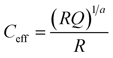 .37 Additionally, each RC-element is associated with a time constant τ of the related process, defined by τ = RC.34,37 Besides this, the spectra show no additional features, except for a small resistive offset typically observed in solar cells and generally attributed to the series resistance of the device.34,35 Consequently, the equivalent circuit chosen to fit the presented impedance data consists of a the aforementioned series resistance and two RQ-elements to represent the two semicircles in the Nyquist plots (see Fig. S9, ESI†).
Fig. 5 depicts the corresponding results from the fitting of the larger semicircle component. The time constants of this process presented in Fig. 5(a) exhibit a very similar behaviour to the ones obtained for the charge carrier lifetimes from the TPV data (compare Fig. 4(a)): they decrease with increasing voltage and show a clear split between the samples containing iodide and the ones incorporating either Br or Cl, for biases exceeding 0.1 V, both in the dark and under illumination. For a direct comparison between absolute values obtained from the two techniques, the conditions need to be chosen carefully though, due to their inherent differences. While during TPV measurements a light bias is used to establish a certain voltage across the cell under open circuit conditions, the offset bias in the impedance spectroscopy is imposed onto the device from an external source, with illumination being an additional factor that would increase the number of generated charge carriers in the system. Therefore, the closest match in conditions seems to be the impedance results at 0.3 V under illumination, together with the TPV data at a similar VOC. Interestingly, these values seem to match very well for all studied devices, as can be observed from Table 4. Thus, it can be concluded that the large semicircle in the impedance data represents the charge carrier recombination and the obtained time constants can be assigned to the carrier lifetimes. The associated resistive component, presented in Fig. 5(b), can therefore be assigned to the recombination resistance. Its overall trends underline the behaviour found for the lifetimes, both under illumination and in the dark. Generally, the recombination resistance in the dark is higher than under illumination, which is caused by the different amount of free charge carriers in the system. With more electrons and hole present in the material, the probability of them encountering each other and recombining is increasing. Contrary to that, the decrease of the recombination resistance with increasing forward bias, is assigned to the typical JV-characteristic a diode-based device, such as a solar cell, normally exhibits. That the observed process is connected to the solar cell junction is further underlined by the capacitive response visible in Fig. 5(c). There, the general trend seems to be an increase in capacitance towards larger forward bias. This matches the expected behaviour of a pn-junction, since its depletion region becomes narrower under forward bias and consequently the associated capacitance increases.35 Contrary to the lifetimes and recombination resistances, the capacitance of the depletion region appears to be less affected by the different ligands employed, with no inherently clear trend or separation being visible.
 | ||
| Fig. 5 Results from impedance spectroscopy fits for the large semicircle: (a) charge carrier lifetimes, (b) recombination resistance and (c) capacitance at different biases under illumination (0.4 sun equivalent) and in the dark. | ||
| TPV | Impedance | |||
|---|---|---|---|---|
| V OC (V) | τ LT (μs) | Bias (V) | τ LT (μs) | |
| TBAI | 0.30 | 14 | 0.30 | 17 |
| TMAI | 0.29 | 19 | 0.30 | 18 |
| TBABr | 0.30 | 55 | 0.30 | 58 |
| TMABr | 0.31 | 49 | 0.30 | 43 |
| TMACl | 0.31 | 54 | 0.30 | 47 |
Next, the fitting results regarding the smaller semicircle included in the model to account for the shoulder visible in the impedance data towards lower frequencies are considered. The calculated time constants associated with this process are depicted in Fig. 6(a) for all conditions explored. They show an overall much flatter response to an increasing forward bias than the lifetimes in Fig. 5(a), complementary to what could be observed from the TPV/TPJ measurements in Fig. 4. Another similarity between the results gained from the two methods is the high overlap between the values obtained for the differently passivated NCs in the devices, making them practically indistinguishable. This is further reinforced by the higher uncertainty these time constants have, due to the large overlap between the two semicircles observed in the impedance spectra and their relative size difference. Hence, the confidence intervals of this part of the fit significantly impacted, as indicated by the error bars in Fig. 6. To verify that the observed process can really be attributed to the charge transport, it is also important to compare the time scale it is occurring on to the previous findings (see Fig. 4(b)). Upon closer inspection, all time constants extracted from impedance spectra measured under illumination range between 2 μs and 7 μs, while the ones calculated from the TPV/TPJ data were found to be between 2 μs and 6 μs. This can be considered a very good match, both with respect to the depicted trends as well as the absolute numbers, implying that the observed process in the impedance spectra are indeed related to the charge transport through the devices. Regarding the different investigated samples, the findings of the impedance spectroscopy also indicate that the exact passivation, within the framework of the tested conditions, seems to have a negligible impact on the charge transport times. However, taking a closer look at the corresponding transport resistance and capacitance displayed in Fig. 6(b) and (c), respectively, there seem to be some subtle differences between the five samples, which would remain undiscovered, if one would only take the transport times from both techniques into consideration. While the overall response of both the resistive and the capacitive component in the dark is rather flat but slightly decreasing for increasing forward bias in all samples, this is not the case for the transport resistance under illumination. There, the trend remains comparatively flat for the iodide-passivated devices, while the ones employing the smaller halides show an enhanced transport resistance under increased bias. Similarly, these samples also show a slightly more pronounced response in the capacitance, which exhibits a simultaneous decrease over the described bias interval. These observations, might hint at a minor difference in the charge transport mechanism or indicate the presence of some limitation in the TBABr-, TMABr- and TMACl-based solar cells with respect to their charge transport. Hence, the previous findings regarding the slightly lower JSC found in those devices might not only be due to the differences in absorber layer thickness, but also impacted by the charge transport, either through the layer or across the adjacent interfaces.
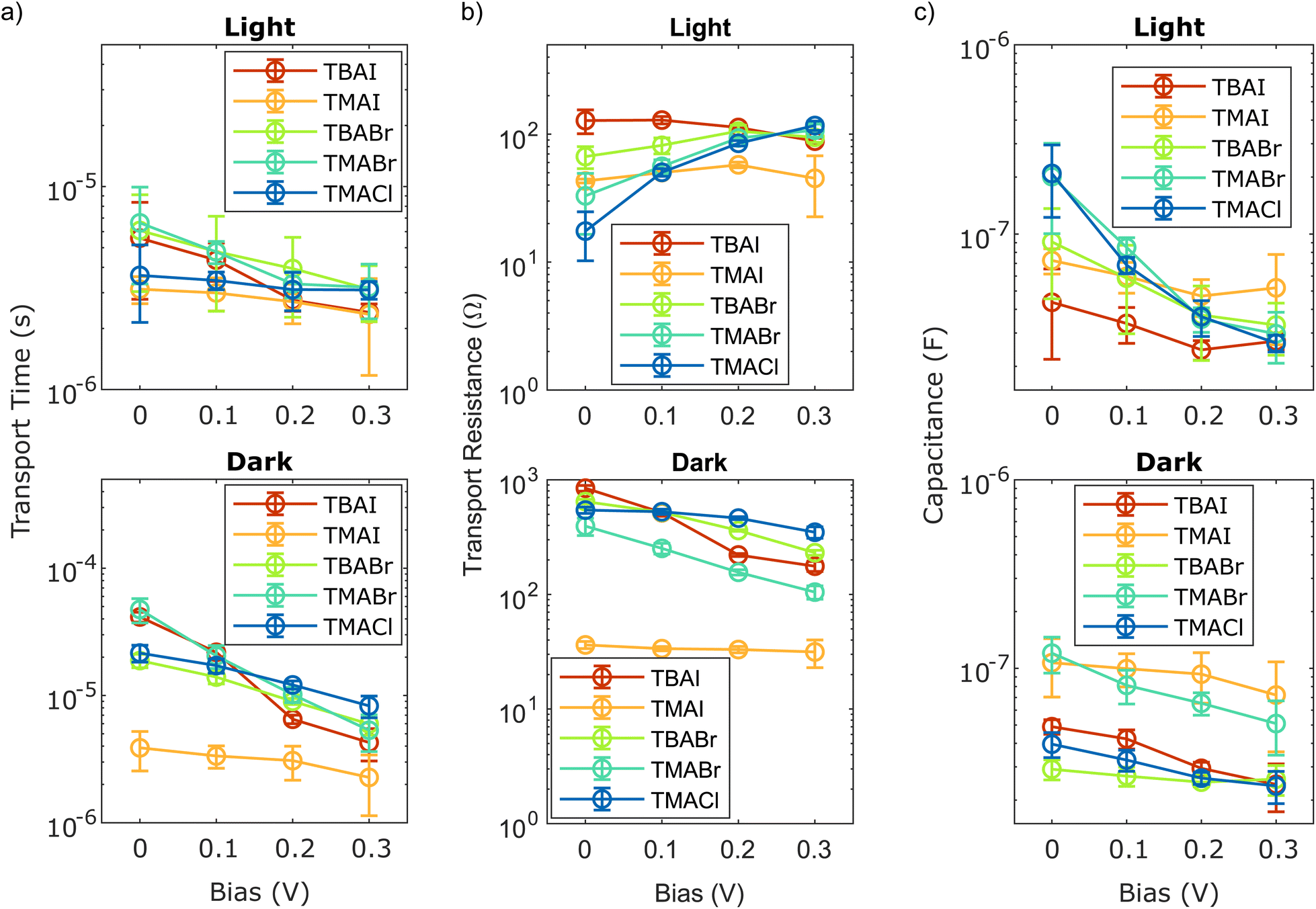 | ||
| Fig. 6 Results from impedance spectroscopy fits for the small semicircle: (a) charge carrier transport times, (b) transport resistance and (c) capacitance at different biases under illumination (0.4 sun equivalent) and in the dark. | ||
3 Conclusions
In this study, an inert-atmosphere-free synthesis method for AgBiS2 NCs has been demonstrated and subsequent device fabrication under ambient conditions allowed for the incorporation of different surface passivating compounds into the photoactive layer via ligand exchange. XPS analysis of the corresponding thin films revealed that the ligand uptake varied greatly, with the iodine from the TBAI and TMAI being incorporated to a much larger extend than the smaller halides from TBABr, TMABr and TMACl. As a result, the latter samples showed signs of a higher degree of surface oxidation instead. Simultaneously, the anomalous low energy component in the Bi 4f signal, previously associated with trap states, got reduced under those conditions. In agreement with this, the VOC values of the related solar cells were found to be higher, while the JSC tends to be slightly lower than the ones found for their TBAI or TMAI counterparts. The latter could at least in part be correlated with a thinner absorber layer thickness. Moreover, both transient measurements and impedance spectroscopy revealed a significant difference in charge carrier lifetimes between the iodide-passivation and NCs treated with TBABr, TMABr or TMACl at a certain voltage, with devices based on the smaller halide ligands outperforming the iodide-based ones. Regarding the charge carrier transport times, all five samples behaved similarly though. However, the associated transport resistance from the impedance spectra gave first insights into differences in either the transport mechanism or potential limits caused by the respective surface passivation. Whether this difference is related to the transport through the AgBiS2 NC layer itself, or an effect of the adjacent interfaces remains unclear at this point and needs to be addressed in future research. Overall, this study highlights the importance of understanding the interplay of QD–ligand interaction due to its significant impact on the overall material properties and thereby on any device employing these materials.4 Materials and methods
4.1 Materials
The following chemicals were purchased from Sigma-Aldrich/Merck and used as received, unless otherwise stated: silver(I) acetate (AgOAc, ≥99.9%), bismuth(III) acetate (BiOAc3, ≥99.99%), sulphur (S, ≥99.5%), oleylamine (OLAm, 70%), oleic acid (OA, 90%), toluene (99.8%), acetone (99.0%), zinc acetate dihydrate (99.5%), ethanolamine (≥99.5%), ethanol (≥99.8%), ITO coated glass (pre-patterned, Zhuhai Kaivo Optoelectronic Technology Co., Ltd), Hellmanex II (concentrate), methanol (≥99.9%), tetrabutylammonium iodide (TBAI, ≥99.0%), tetramethylammonium iodide (TMAI, 99%), tetrabutylammonium bromide (TBABr, 99%), tetramethylammonium bromide (TMABr, ≥98.0%), tetramethylammonium chloride (TMACl, ≥98.0%), poly(3-hexylthiophene-2,5-diyl) (P3HT, regioregular), chlorobenzene (99.8%), molybdenum(VI) oxide (MoO3, 99.98%), Ag.4.2 Methods
:1) with toluene and injected into the reaction mixture at 100 °C. Then, the resulting crude NC dispersion was transferred to a stirring plate and left there too cool down to RT for 20 min. Acetone was used as the anti-solvent to precipitate the NCs from the reaction mixture, followed by centrifugation (8000 rpm, 10 min), discarding of the supernatant and subsequent redispersion in toluene. This precipitation–redispersion cycle was repeated once more for further purification. Lastly, the redispersed NCs were centrifuged (3000 rpm, 10 min) without the addition of the anti-solvent to remove any potential bulk material and/or agglomerates. The concentration of the supernatant was afterwards adjusted to 20 mg mL−1 for storage under ambient conditions and further use in the device fabrication and characterisations.
4.2.4.1 JV-Measurements. JV-Characteristics of the finished devices were obtained from a Wavelabs Sinus-70 solar simulator to imitate AM1.5G conditions. The variation of the illumination intensities for certain measurements was done via calibrating for different surface energies of the same spectrum, with the correlation x kW m−2 = x sun.
4.2.4.2 IPCE. IPCE spectra were measured with an in-house built setup, as described previously.7,38,39 In short, it is comprised of a xenon lamp (Spectral Products, ASB-XE-175), monochromator (Spectral Products, CM110), automatic filter wheel (Spectral Products, AB301-T) potentiostat (PINE, AFRDE 5), beam splitter (ThorLabs), silicon photodiode (ThorLabs, SM1PD2A) and a LabJack U6 data acquisition device. The calibration was carried out with a second silicon photodiode (ThorLabs, SM1PD2A).
4.2.4.3 TPV/TPJ measurements. Transient photovoltage and photocurrent measurements were carried out on a modular setup, according to previous descriptions.39–42 To summarise, a white LED lamp (Luxeon Star 1 W) was used for as a light source and its light intensity was calibrated using a certified reference solar cell (Frauenhofer ISE) prior to measurements. The photocurrent and photovoltage transients were obtained by applying a small square wave modulation to the base light intensity and recording the corresponding traces with the help of a current amplifier (Stanford Research System SR570), a 16 bit resolution digital acquisition board and a custom-made system of electromagnetic switches. The resulting data was normalised and fit with a single exponential to obtain the related time constants.
4.2.4.4 Impedance spectroscopy. Impedance spectroscopy was carried out on the complete solar cell devices, using an IVIUM h.Stat instrument. The frequency was scanned from 1 MHz to 1 Hz with an amplitude of 10 mV. Measurements conditions were varied regarding the offset bias (0.0–0.3 V) and illumination (darkness or 0.4 sun equivalent) of the devices.
4.2.4.5 SEM. SEM cross-sections were prepared by breaking apart a finished solar cell device immediately before the measurement. The images were taken in vacuum on a Zeiss LEO 1530 instrument, equipped with an in-lens detector. The acceleration voltage was set to 2 kV, with working distances between 4 mm and 5 mm.
4.2.5.1 UV-vis-NIR spectroscopy. UV-vis-NIR absorption spectroscopy was carried out on a Carry 5000 spectrometer for both OA/OLAm-capped colloidal NCs in toluene, as well as for the ligand-exchanged thin films, fabricated identically to the method described in the device fabrication.
4.2.5.2 XPS/UPS. XPS and UPS was used to characterise the ligand-exchanged thin films, fabricated identically to the method described in the device fabrication with the only exception that the AgBiS2 NCs were deposited directly onto the ITO substrate without the ZnO ETL in-between. The measurements took place on a Kratos AXIS Supra+, equipped with an Al Kα anode (photon energy: 1486.7 eV) and a helium discharge lamp (photon energy: He I 21.22 eV) for XPS and UPS, respectively. The XPS spectra were energy calibrated to the Fermi level by measuring the Au 4f core level of a gold reference and setting the Au 4f7/2 level to 84.0 eV. For UPS, the Fermi edge energy was determined directly from the same gold reference. Curve fitting of the XPS core level signals was done in Casa XPS.43 There, pseudo-Voigt functions were used in combination with a Shirley background for all signals. From the UPS data, the valence band maximum and the work function were determined from the high- and low-binding-energy-cutoffs, respectively. These were obtained via linear fitting and extrapolation according to a previously published method.5
4.2.5.3 XRD. X-ray diffractograms were obtained from OA/OLAm passivated AgBiS2 NCs drop-cast onto amorphous glass substrates. The measurements were carried out in a grazing incidence configuration on a Siemens D5000. The incident angle was set to 3° and measurements were carried out between 10° and 85° (2θ) using a Cu Kα X-ray source.
4.2.5.4 TEM. For the TEM images, the NC dispersion in toluene was diluted to 2 mg mL−1 and dropped on formvar/carbon covered Cu-grids (200 Mesh, TED PELLA Inc.). The measurement took place on a FEI Titan Themis 200, operated at 200 kV acceleration voltage.
Data availability
All data are included in the manuscript either in the main text manuscript, or in the ESI† available for the readers.Conflicts of interest
There are no conflicts to declare.Acknowledgements
This work was funded by the Swedish Research Council (VR), Swedish Energy Agency, and Olle Engkvist Foundation. This work was partially supported by the Wallenberg Initiative Materials Science for Sustainability (WISE) funded by the Knut and Alice Wallenberg Foundation. We thank Dr Leif Häggman for technical support. We acknowledge Myfab Uppsala for providing facilities and experimental support. Myfab is funded by the Swedish Research Council (2019-00207) as a national research infrastructure.Notes and references
- D. V. Talapin, J. S. Lee, M. V. Kovalenko and E. V. Shevchenko, Chem. Rev., 2010, 110, 389–458 Search PubMed.
- M. Yuan, M. Liu and E. H. Sargent, Nat. Energy, 2016, 1, 16016 CrossRef CAS.
- G. H. Carey, A. L. Abdelhady, Z. Ning, S. M. Thon, O. M. Bakr and E. H. Sargent, Chem. Rev., 2015, 115, 12732–12763 CrossRef CAS PubMed.
- M. Liu, O. Voznyy, R. Sabatini, F. P. García De Arquer, R. Munir, A. H. Balawi, X. Lan, F. Fan, G. Walters, A. R. Kirmani, S. Hoogland, F. Laquai, A. Amassian and E. H. Sargent, Nat. Mater., 2017, 16, 258–263 Search PubMed.
- P. R. Brown, D. Kim, R. R. Lunt, N. Zhao, M. G. Bawendi, J. C. Grossman and V. Bulović, ACS Nano, 2014, 8, 5863–5872 CrossRef CAS PubMed.
- M. Bernechea, N. C. Miller, G. Xercavins, D. So, A. Stavrinadis and G. Konstantatos, Nat. Photonics, 2016, 10, 521–525 CrossRef CAS.
- V. A. Öberg, M. B. Johansson, X. Zhang and E. M. Johansson, ACS Appl. Nano Mater., 2020, 3, 4014–4024 CrossRef.
- J. T. Oh, S. Y. Bae, S. R. Ha, H. Cho, S. J. Lim, D. W. Boukhvalov, Y. Kim and H. Choi, Nanoscale, 2019, 11, 9633–9640 Search PubMed.
- M. Z. Akgul, A. Figueroba, S. Pradhan, Y. Bi and G. Konstantatos, ACS Photonics, 2020, 7, 588–595 Search PubMed.
- D. Chen, S. B. Shivarudraiah, P. Geng, M. Ng, C. H. Li, N. Tewari, X. Zou, K. S. Wong, L. Guo and J. E. Halpert, ACS Appl. Mater. Interfaces, 2022, 14, 1634–1642 Search PubMed.
- J. T. Oh, S. Y. Bae, J. Yang, S. R. Ha, H. Song, C. B. Lee, S. Shome, S. Biswas, H.-M. Lee, Y.-H. Seo, S.-I. Na, J.-S. Park, W. Yi, S. Lee, K. Bertens, B. R. Lee, E. H. Sargent, H. Kim, Y. Kim and H. Choi, J. Power Sources, 2021, 514, 230585 CrossRef CAS.
- I. Burgués-Ceballos, Y. Wang, M. Z. Akgul and G. Konstantatos, Nano Energy, 2020, 75, 104961 CrossRef.
- L. Hu, R. J. Patterson, Z. Zhang, Y. Hu, D. Li, Z. Chen, L. Yuan, Z. L. Teh, Y. Gao, G. J. Conibeer and S. Huang, J. Mater. Chem. C, 2018, 6, 731–737 Search PubMed.
- Y. Wang, S. R. Kavanagh, I. Burgués-Ceballos, A. Walsh, D. O. Scanlon and G. Konstantatos, Nat. Photonics, 2022, 16, 235–241 CrossRef CAS.
- O. Voznyy, D. Zhitomirsky, P. Stadler, Z. Ning, S. Hoogland and E. H. Sargent, ACS Nano, 2012, 6, 8448–8455 CrossRef CAS PubMed.
- N. C. Anderson, M. P. Hendricks, J. J. Choi and J. S. Owen, J. Am. Chem. Soc., 2013, 135, 18536–18548 Search PubMed.
- M. A. Boles, D. Ling, T. Hyeon and D. V. Talapin, Nat. Mater., 2016, 15, 141–153 CrossRef CAS PubMed.
- Y. Liu, M. Gibbs, J. Puthussery, S. Gaik, R. Ihly, H. W. Hillhouse and M. Law, Nano Lett., 2010, 10, 1960–1969 CrossRef CAS PubMed.
- S. Y. Bae, J. T. Oh, J. Y. Park, S. R. Ha, J. Choi, H. Choi and Y. Kim, Chem. Mater., 2020, 32, 10007–10014 CrossRef CAS.
- Y. Wang, L. Peng, Z. Wang and G. Konstantatos, Adv. Energy Mater., 2022, 12, 2200700 Search PubMed.
- J. W. Thomson, K. Nagashima, P. M. MacDonald and G. A. Ozin, J. Am. Chem. Soc., 2011, 133, 5036–5041 Search PubMed.
- J. Zhang, J. Gao, E. M. Miller, J. M. Luther and M. C. Beard, ACS Nano, 2014, 8, 614–622 Search PubMed.
- J. T. Oh, H. Cho, S. Y. Bae, S. J. Lim, J. Kang, I. H. Jung, H. Choi and Y. Kim, Int. J. Energy Res., 2020, 44, 11006–11014 CrossRef CAS.
- S. Geller and J. H. Wernick, Acta Crystallogr., 1959, 12, 46–54 Search PubMed.
- H. Beygi, S. A. Sajjadi, A. Babakhani, J. F. Young and F. C. van Veggel, Appl. Surf. Sci., 2018, 457, 1–10 CrossRef CAS.
- I. Moreels, Y. Justo, B. D. Geyter, K. Haustraete, J. C. Martins and Z. Hens, ACS Nano, 2012, 5, 2004–2012 CrossRef PubMed.
- R. G. Pearson, J. Am. Chem. Soc., 1963, 85, 3533–3539 CrossRef CAS.
- V. K. Kaushik, J. Electron Spectrosc. Relat. Phenom., 1991, 56, 273–277 CrossRef CAS.
- M. Bernechea, Y. Cao and G. Konstantatos, J. Mater. Chem. A, 2015, 3, 20642–20648 RSC.
- D. S. Zingg and D. M. Hercules, J. Phys. Chem., 1978, 82, 1992–1995 CrossRef CAS.
- R. D. Seals, R. Alexander, L. T. Taylor and J. G. Dillard, Inorg. Chem., 1973, 12, 2485–2487 CrossRef CAS.
- J. Vollbrecht and V. V. Brus, Org. Electron., 2020, 86, 105905 Search PubMed.
- L. Etgar, T. Moehl, S. Gabriel, S. G. Hickey, A. Eychmüller and M. Grätzel, ACS Nano, 2012, 6, 3092–3099 Search PubMed.
- E. Von Hauff, J. Phys. Chem. C, 2019, 123, 11329–11346 Search PubMed.
- H. Wang, Y. Wang, B. He, W. Li, M. Sulaman, J. Xu, S. Yang, Y. Tang and B. Zou, ACS Appl. Mater. Interfaces, 2016, 8, 18526–18533 Search PubMed.
- A. K. Rath, T. Lasanta, M. Bernechea, S. L. Diedenhofen and G. Konstantatos, Appl. Phys. Lett., 2014, 104, 063504 CrossRef.
- G. J. Brug, A. L. van den Eeden, M. Sluyters-Rehbach and J. H. Sluyters, J. Electroanal. Chem., 1984, 176, 275–295 CrossRef CAS.
- V. A. Öberg, X. Zhang, M. B. Johansson and E. M. Johansson, ChemNanoMat, 2018, 4, 1223–1230 CrossRef.
- X. Zhang, J. Zhang, D. Phuyal, J. Du, L. Tian, V. A. Öberg, M. B. Johansson, U. B. Cappel, O. Karis, J. Liu, H. Rensmo, G. Boschloo and E. M. Johansson, Adv. Energy Mater., 2018, 8, 1–11 Search PubMed.
- X. Zhang, J. Liu, J. Zhang, N. Vlachopoulos and E. M. Johansson, Phys. Chem. Chem. Phys., 2015, 17, 12786–12795 RSC.
- L. Yang, U. B. Cappel, E. L. Unger, M. Karlsson, K. M. Karlsson, E. Gabrielsson, L. Sun, G. Boschloo, A. Hagfeldt and E. M. Johansson, Phys. Chem. Chem. Phys., 2012, 14, 779–789 RSC.
- S. M. Feldt, E. A. Gibson, E. Gabrielsson, L. Sun, G. Boschloo and A. Hagfeldt, J. Am. Chem. Soc., 2010, 132, 16714–16724 CrossRef CAS PubMed.
- N. Fairley, V. Fernandez, M. Richard-Plouet, C. Guillot-Deudon, J. Walton, E. Smith, D. Flahaut, M. Greiner, M. Biesinger, S. Tougaard, D. Morgan and J. Baltrusaitis, Applied Surface Science Advances, 2021, 5, 100112 CrossRef.
Footnote |
| † Electronic supplementary information (ESI) available. See DOI: https://doi.org/10.1039/d4ta04481a |
| This journal is © The Royal Society of Chemistry 2024 |