
 Open Access Article
 This Open Access Article is licensed under a Creative Commons Attribution-Non Commercial 3.0 Unported Licence
Synergetic enhancement of CsPbI3 nanorod-based high-performance photodetectors via PbSe quantum dot interface engineering†
Muhammad
Sulaman
 abc,
Shengyi
Yang
*ab,
Honglian
Guo
c,
Chuanbo
Li
c,
Ali
Imran
d,
Arfan
Bukhtiar
e,
Muhammad
Qasim
f,
Zhenhua
Ge
ab,
Yong
Song
f,
Yurong
Jiang
f and
Bingsuo
Zou
e
abc,
Shengyi
Yang
*ab,
Honglian
Guo
c,
Chuanbo
Li
c,
Ali
Imran
d,
Arfan
Bukhtiar
e,
Muhammad
Qasim
f,
Zhenhua
Ge
ab,
Yong
Song
f,
Yurong
Jiang
f and
Bingsuo
Zou
e
aBeijing Key Lab of Nanophotonics and Ultrafine Optoelectronic Systems, Center for Micro-Nanotechnology, School of Physics, Beijing Institute of Technology, Beijing 100081, P. R. China. E-mail: syyang@bit.edu.cn
bKey Lab of Advanced Optoelectronic Quantum Design and Measurement, Ministry of Education, School of Physics, Beijing Institute of Technology, Beijing 100081, P. R. China
cOptoelectronics Research Center, School of Science, Minzu University of China, Beijing, 100081, China
dSchool of Micro-Nanoelectronics, ZJU-Hangzhou Global Scientific and Technological Innovation Center, State Key Labs of Silicon Materials and Modern Optical Instrumentation, Zhejiang University, Hangzhou 311200, China
eMOE Key Lab of New Processing Technology for Nonferrous Metals and Materials and Guangxi Key Lab of Processing for Nonferrous Metals and Featured Materials, School of Resources, Environments and Materials, Guangxi University, Nanning 530004, P. R. China
fBeijing Key Lab for Precision Optoelectronic Measurement Instrument and Technology, School of Optics and Photonics, Beijing Institute of Technology, Beijing 100081, P. R. China
First published on 30th April 2024
Abstract
The advancement of optoelectronic applications relies heavily on the development of high-performance photodetectors that are self-driven and capable of detecting a wide range of wavelengths. CsPbI3 nanorods (NRs), known for their outstanding optical and electrical properties, offer direct bandgap characteristics, high absorption coefficients, and long carrier diffusion lengths. However, challenges such as stability and limited photoluminescence quantum yield have impeded their widespread application. By integrating PbSe colloidal quantum dots (CQDs) with CsPbI3 NRs, the hybrid nanomaterial harnesses the benefits of each component, resulting in enhanced optoelectronic properties and device performance. In this work, a self-powered and broadband photodetector, ITO/ZnO/CsPbI3:PbSe/CuSCN/Au, is fabricated, in which CsPbI3 NRs are decorated with PbSe QDs as the photoactive layer, ZnO as the electron-transporting layer and CuSCN as the hole-transporting layer. The device performance is further improved through the incorporation of Cs2CO3 into the ZnO layer, resulting in an enhancement of its overall operational characteristics. As a result, a notable responsivity of 9.29 A W−1 and a specific detectivity of 3.17 × 10¹⁴ Jones were achieved. Certainly, the TCAD simulations closely correlate with our experimental data, facilitating a comprehensive exploration of the fundamental physical mechanisms responsible for the improved performance of these surface-passivated heterojunction photodetectors. This opens up exciting possibilities for substantial advancements in the realm of next-generation optoelectronic devices.
1. Introduction
High-performance photodetectors with a broad spectrum response and self-driven behavior are in high demand due to the quick advancements in optoelectronic technology.1–3 Photodetectors play a pivotal role in various applications, including imaging, sensing, communication systems, and environmental monitoring.4,5 Efficient detection of light across a wide range of wavelengths is essential for capturing and converting optical signals into electrical signals with high sensitivity and accuracy. The development of high-performance photodetectors with a broad spectral response and self-driven behavior is of great significance in advancing these technologies.6–8 The advancement of optoelectronic materials and device architectures has led to significant improvements in their performance, enabling enhanced sensitivity, efficiency, and stability. Hybrid nanocomposites, composed of different nanoscale building blocks, have emerged as promising materials for achieving enhanced photodetection capabilities. By combining different nanomaterials in a hybrid nanocomposite, complementary absorption characteristics can be exploited, enabling the detection of a wide range of wavelengths.9–12 One promising platform that has emerged in recent years is based on CsPbI3 nanorods (NRs) decorated with PbSe colloidal quantum dots (CQDs). This hybrid nanomaterial combines the unique properties of both CsPbI3 NRs and PbSe CQDs, resulting in synergistic effects that enhance the optoelectronic properties and overall device performance.CsPbI3 NRs have attracted considerable attention due to their outstanding optical and electrical properties. These NRs exhibit direct bandgap characteristics, high absorption coefficients, and long carrier diffusion lengths, making them highly efficient in light absorption and carrier transportation.13–16 Additionally, CsPbI3 NRs, known for their outstanding optical and electrical properties, offer direct bandgap characteristics, high absorption coefficients, and long carrier diffusion lengths. However, challenges such as stability, particularly in the presence of moisture and oxygen, and limited photoluminescence quantum yield have impeded their widespread application.17–19 To overcome these limitations and further improve the performance of CsPbI3-based photodetectors such as enabling an enhanced absorption range, efficient charge transfer, improved stability and overall device performance, the integration of PbSe CQDs has been explored. PbSe CQDs possess tunable bandgaps and strong infrared (IR) light absorption properties, making them ideal sensitizers for broadening the light absorption range of the CsPbI3 NRs.20–23 By incorporating PbSe CQDs into the CsPbI3 NRs, efficient charge transfer can be achieved, reducing carrier recombination and enhancing the overall device performance. Hybrid nanocomposites of CsPbI3 NRs with inorganic materials offer advantages such as broad spectral response, complementary absorption characteristics, enhanced charge transport, tunable bandgap, and compatibility with various device architectures.24 These advantages make hybrid nanocomposites highly promising for the development of efficient and versatile optoelectronic devices such as photodetectors and solar cells. One significant advantage of the CsPbI3 NRs decorated with PbSe CQDs (i.e. CsPbI3:PbSe) is the enhanced photoresponsivity of the photodetectors. The incorporation of PbSe CQDs facilitates efficient light absorption over a broader spectral range, including the infrared region, thereby increasing the overall responsivity of the device. This enhanced responsivity is crucial for applications requiring high sensitivity to low light levels.
A hybrid nanocomposite of PbSe QDs with CsPbI3 offers a strategic approach to combine the strengths of each material, resulting in a hybrid nanocomposite that efficiently captures a wide range of wavelengths, promotes effective charge transfer, and enhances the overall performance and stability of the optoelectronic device.25,26 The incorporation of CsPbI3 NRs and PbSe CQDs in the hybrid nanomaterial results in enhanced specific detectivity by reducing carrier recombination and improving charge transfer efficiency. Specific detectivity is a crucial parameter for photodetectors, as it quantifies their ability to detect weak optical signals in the presence of noise. The presence of PbSe CQDs enhances the generation of photocurrent, resulting in higher detectivity.27 This improved detectivity is advantageous for applications where the detection of weak signals is essential. Therefore, the interpenetration of PbSe CQDs and CsPbI3 NRs in the hybrid nanomaterial promotes efficient charge transfer, enhanced light absorption, and minimized charge recombination. These factors contribute to the improved performance and functionality of the photodetectors based on this hybrid nanomaterial structure. Furthermore, the hybrid structure of CsPbI3 NRs decorated with PbSe CQDs offers improved stability and environmental tolerance as compared to pristine CsPbI3 NRs.28 Therefore, CsPbI3 NRs act as a stable framework, preventing the aggregation of PbSe CQDs and preserving their optoelectronic properties over time. This stability is crucial for long-term device operation and reliability. Additionally, the incorporation of PbSe CQDs mitigates hysteresis effects, which can degrade the performance of photodetectors.
Therefore, we combine the unique optical and electrical properties of CsPbI3 NRs with the tunable bandgaps and charge transfer capabilities of PbSe QDs. This hybrid approach aims to address challenges such as the limited photoluminescence quantum yield (PLQY) and stability of CsPbI3 NRs, ultimately leading to enhanced optoelectronic properties and device performance. Thus, photodetectors ITO/ZnO/CsPbI3:PbSe/CuSCN/Au were fabricated and investigated, in which the ZnO layer serves as an electron-transporting layer (ETL), thus facilitating the efficient extraction and transport of electrons generated by the absorbed light. Cs2CO3, being an alkaline compound as a dopant in the ZnO matrix, can alter the energy levels and carrier concentration in the film, leading to reduced dark current and enhanced photocurrent. After blending Cs2CO3 with ZnO nanocrystals, additional charge carriers are introduced into the film, increasing the electron density effectively,29,30 resulting in improved electron mobility and reduced trap-assisted recombination, and thus decreasing the dark current. The reduced dark current helps to minimize the noise level and improve the signal-to-noise ratio of the device. The hybrid nanocomposite of the CsPbI3:PbSe layer serves as the photoactive material in the photodetector, combining the CsPbI3 NRs with PbSe CQDs. This hybrid nanocomposite layer offers a broad spectral response and efficient charge generation due to the complementary absorption properties of each component. The CuSCN layer acts as the hole-transporting layer, enabling efficient extraction and transport of holes generated by the absorbed photon density. Under illumination, the device can effectively absorb the incident light, photogenerated excitons will dissociate into electrons and holes, and buffer layers will facilitate their efficient extraction and transportation. Consequently, the self-driven photodetector yielded a substantial ON/OFF current ratio of 103, accompanied by an exceptional photosensitivity of 9.97 × 10³. Additionally, a specific detectivity of 5.22 × 10¹³ Jones with a photoresponsivity of 2.87 A W−1 was achieved under 980 nm laser illumination. The performance of the device has been improved through incorporating Cs2CO3 into the ZnO layer (i.e. ZnO:Cs2CO3). Consequently, this integration has led to a notable enhancement in the overall device performance. This heterojunction structure allows for optimized charge carrier dynamics, resulting in enhanced photodetection performance. The fabricated photodetector is characterized and evaluated in terms of key performance parameters such as photosensitivity, photoresponsivity, specific detectivity, and response time. The results obtained from the fabricated device provide valuable insights into the performance and potential applications of this specific photodetector structure. A high ON/OFF ratio of 105, a super-high photosensitivity of 7.25 × 10⁴, photoresponsivity of 9.29 A W−1 and specific detectivity of 3.17 × 10¹⁴ Jones were obtained from the photodetector ITO/ZnO:Cs2CO3/CsPbI3:PbSe/CuSCN/Au in the self-driven mode under 80 μW cm−2 980 nm illumination. Here, the ETL was improved by blending ZnO with CsCO3 in a suitable ratio in order to further enhance the device performance. The specific blending ratio and the subsequent fabrication steps may vary depending on the specific experimental conditions and objectives.
Further, technology computer-aided design (TCAD) simulation was performed to further investigate and analyze the performance of the fabricated photodetector. TCAD software allows for the modeling and simulation of device behavior, providing a detailed understanding of the underlying physics and aiding in optimizing device design and performance. This allowed for a deeper understanding of the device physics, including charge carrier dynamics, distribution, and transport, as well as the impact of different device parameters and material properties.
2. Experimental section
2.1 Synthesis of ZnO nanoparticles
ZnO nanoparticles were synthesized by a sol–gel method to ensure the production of high-quality nanocrystals by following the previously reported method.31 The detailed synthesis method is described in Note S1 (in the ESI).†2.2 Synthesis of PbSe CQDs
PbSe CQDs were prepared by a previously reported hot-injection method with some modifications.20,21 The detailed synthesis procedure is briefly described in Note S2 (in the ESI).†2.3 Synthesis of CsPbI3 NRs
The synthesis of CsPbI3 NRs involved the integration of emulsion and the tip-ultrasonic method. Initially, precursor materials, including 0.814 g of Cs2CO3 and 1.8 mmol of PbI2, were dissolved in a mixture comprising 40 mL of ODE, 2.5 mL of OA, and 2.5 mL of oleylamine (OAm) within a capped flask, and subjected to continuous stirring at 100 °C for 1 hour, following the procedure outlined by Protesescu et al.32 Subsequently, the tip-ultrasonication rod was immersed into the reaction flask at 90 °C for a duration of 20 minutes. Rapid cooling was achieved using an ice-water bath. The resultant cooled solution was subjected to centrifugation at 6500 rpm for 10 minutes, yielding separated and collected particles, which were then re-dispersed in n-hexane or chlorobenzene.2.4 Device fabrication and characterization
The process of fabricating and characterizing the devices involved several steps. Initially, the ITO patterned glass substrate was thoroughly cleaned and treated with UV-ozone light. A layer of ZnO NCs was then spin-coated onto the pre-cleaned glass/ITO substrate and annealed at 80 °C for 30 minutes, serving as the ETL. Next, PbSe CQDs and CsPbI3 NCs were separately dissolved in chlorobenzene (20 mg mL−1) to form solutions. These solutions were combined in different volume ratios, resulting in the formation of a nanocomposite solution of CsPbI3:PbSe. The optimal volume ratio of 1![[thin space (1/6-em)]](https://www.rsc.org/images/entities/char_2009.gif) :0.5 was determined, considering its advantages of low dark current and high absorption capability. The resulting nanocomposite solution was then spin-coated onto the ETL of the ZnO layer at 1000 rpm for 30 seconds and annealed at 80 °C for 1 hour. This process facilitated the formation of the nanocomposite layer on the surface. To modify the surface properties of the ETL, Cs2CO3 was integrated with ZnO. The thickness of the active layer increased after treating the CsPbI3:PbSe layer with a solution containing 3-mercaptopropionic acid (MPA) dissolved in acetonitrile. To create a hole-transporting layer, a solution of CuSCN (15 mg mL−1) was spin-coated onto the active layer. Finally, an Au electrode was fabricated on the top surface of the device through thermal evaporation. This step completed the construction of the photodetector.
:0.5 was determined, considering its advantages of low dark current and high absorption capability. The resulting nanocomposite solution was then spin-coated onto the ETL of the ZnO layer at 1000 rpm for 30 seconds and annealed at 80 °C for 1 hour. This process facilitated the formation of the nanocomposite layer on the surface. To modify the surface properties of the ETL, Cs2CO3 was integrated with ZnO. The thickness of the active layer increased after treating the CsPbI3:PbSe layer with a solution containing 3-mercaptopropionic acid (MPA) dissolved in acetonitrile. To create a hole-transporting layer, a solution of CuSCN (15 mg mL−1) was spin-coated onto the active layer. Finally, an Au electrode was fabricated on the top surface of the device through thermal evaporation. This step completed the construction of the photodetector.
Characterization of the fabricated device was performed using specific tools, the details of which are mentioned in Note S3 (in the ESI).† Comprehensive information regarding the TCAD simulation procedures can be found in Note S4 (in the ESI).† This ESI document† offers a detailed account of the methodologies, models, and parameters employed in the TCAD simulations. By referencing Note S4,† readers can gain a thorough understanding of the intricacies involved in our computational investigations, including the specific models used to analyze the absorbed photon density, optical generation, and electrical behavior within the various components of the photodetectors.
3. Results and discussion
The optical properties of CsPbI3 NRs and PbSe QDs were investigated using UV-vis absorption spectroscopy. Fig. 1a shows that the UV-vis and PL spectra of CsPbI3 NRs exhibit a strong absorption peak in the visible range, which is attributed to their direct bandgap characteristics. Fig. 1b shows the absorption spectra of pristine PbSe CQDs and their physically blended nanocomposite with CsPbI3 NRs (i.e. CsPbI3:PbSe). The absorption onset of PbSe QDs occurs in the IR region due to their tunable bandgap properties. The combination of CsPbI3 NRs and PbSe QDs results in broadened absorption characteristics, covering both the visible and IR regions. This synergistic absorption behavior is crucial for enhancing the overall spectral response of the hybrid nanocomposite. To assess the stability of CsPbI3 and PbSe, UV absorption spectra were monitored over varying time intervals. UV absorption spectra were subsequently collected at regular time intervals, ranging from the first day to 30 days for CsPbI3 NRs and from the first day to 6 months for PbSe QDs, to observe any changes in absorption characteristics as shown in Fig. S1 and S2 (in the ESI).† Each measurement involved scanning the samples over a designated wavelength range, typically covering the UV-vis-NIR region relevant to the absorption properties of the materials. The UV-vis absorption spectra of CsPbI3 NRs and PbSe QDs are presented at various time points, highlighting the materials' absorption behavior over time. These spectra provide insights into the stability of these nanomaterials under specific environmental conditions. The comparison of spectra at different time points assists in evaluating the long-term stability of CsPbI3 NRs and PbSe QDs for optoelectronic applications. The optical properties of the pristine ZnO NPs, Cs2CO3, and their blended composite were also characterized by UV-vis absorption spectroscopy, as shown in Fig. 1c. The UV spectrum analysis provides insights into the energy bandgaps, absorption onset, and electronic transitions of the materials, contributing to a comprehensive understanding of their optical behavior.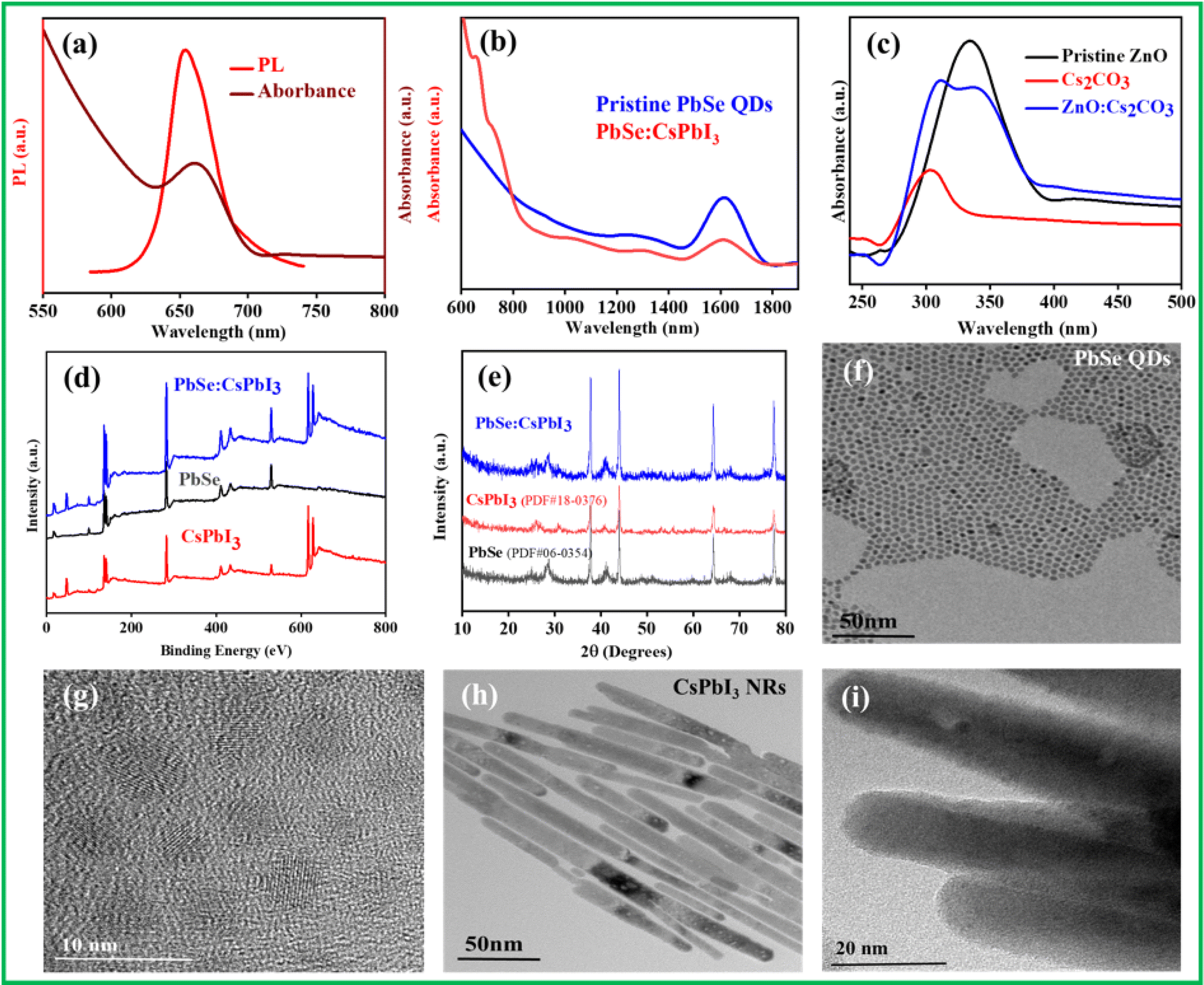 | ||
| Fig. 1 Absorption and PL spectra of the as-synthesized CsPbI3 NRs (a), absorption spectra of pristine PbSe QDs and their blended hybrid CsPbI3:PbSe nanocomposite (b), and pristine ZnO NPs and their hybrid Cs2CO3:ZnO nanocomposites (c). XPS spectra of pristine PbSe QDs, CsPbI3 NRs and their CsPbI3:PbSe nanocomposite (d). XRD patterns of PbSe QDs, CsPbI3 NCs, and their hybrid nanocomposites (e). TEM image of pristine PbSe QDs (f), and HRTEM image of PbSe QDs (g). TEM image of the pristine CsPbI3 NRs (h), and the HRTEM image of CsPbI3 NRs (i). | ||
Moreover, XPS analysis was employed to investigate the surface chemical composition and elemental states of CsPbI3 NRs and PbSe QDs and the hybrid CsPbI3:PbSe nanocomposite, as shown in Fig. 1d. The CsPbI3 NRs show distinct peaks corresponding to Cs, Pb, and I elements, confirming the presence of the perovskite composition. PbSe QDs exhibit peaks corresponding to Pb and Se elements. The binding energies and intensity ratios of these peaks provide insights into the chemical states and stoichiometry of the materials. The XPS analysis confirms the chemical composition of the individual components, which is crucial for understanding the subsequent interactions at the nanocomposite interface. The XPS spectrum of the hybrid nanocomposite of CsPbI3:PbSe shows the superposition of both materials showing all the peaks of both materials in the actual position, which indicates the physical blending of PbSe QDs with CsPbI3 NRs. Fig. S3† shows the XPS spectra of all individual components with their orbital orientations. The crystallographic structure of CsPbI3 NRs and PbSe QDs was investigated by conducting X-Ray Diffraction (XRD) analysis. Fig. 1e shows the XRD patterns of these nanomaterials. The XRD pattern of CsPbI3 NRs confirms their perovskite crystalline structure. The diffraction peaks correspond to the crystallographic planes, indicating the high crystallinity of CsPbI3 NRs. Similarly, the XRD pattern of PbSe QDs verifies their nanocrystalline nature. The observed diffraction peaks align with the expected crystallographic phases. The compatibility of the crystal structures of CsPbI3 NRs and PbSe QDs is essential for achieving a well-integrated hybrid nanocomposite showing their suitable physical blending. Transmission Electron Microscopy (TEM) imaging was employed to visualize the morphology and nanostructure of CsPbI3 NRs and PbSe QDs. Fig. 1f and g show the TEM and high-resolution TEM (HRTEM) images of the PbSe QDs, while Fig. 1h and i show the TEM and HRTEM images of CsPbI3 NRs. The TEM images reveal the nanorod morphology of CsPbI3 NRs in well-defined dimensions with an average diameter of 10 nm. PbSe QDs exhibit a spherical morphology with a dimeter size of 5 nm, which is consistent with the synthesis method. The size distribution plots of both nanomaterials are shown in Fig. S4 and S5.† The spatial distribution of PbSe QDs on CsPbI3 NRs and their interfacial interactions are crucial for facilitating charge transfer processes and improving the overall optoelectronic properties of the hybrid structure.
Fig. 2a displays the scanning electron microscopy (SEM) image of the PbSe QD layer. The image reveals the surface morphology of PbSe QDs, showing their nanoscale size and colloidal nature. The dots exhibit a characteristic uniformity and distribution with high roughness, indicating a controlled synthesis process. The size and shape of the QDs can play a crucial role in their optoelectronic properties, including absorption and charge transport characteristics. Fig. 2b presents the SEM image of CsPbI3 NRs. The image offers insights into the morphology and structure of the CsPbI3 NR film. The nanorods exhibit an elongated geometry with a well-defined aspect ratio. The uniformity and alignment of the nanorods indicate the controlled growth process with their exceptional optical and electrical properties, making them promising candidates for optoelectronic applications. In Fig. 2c, the SEM image of ZnO NPs is displayed. The image shows the morphology of the ZnO nanoparticles, which typically exhibit a nanoscale size with a characteristic spherical or quasi-spherical shape. The ZnO NP film as an ETL plays a pivotal role in their charge transporting properties and their role as an ETL in optoelectronic devices. Fig. 2d provides the SEM image of the blended ZnO:Cs2CO3 nanocomposites. The image offers insights into the morphology of the nanocomposite film, where ZnO nanoparticles are blended with Cs2CO3 (i.e. ZnO:Cs2CO3). The resulting ZnO:Cs2CO3 nanocomposite is expected to exhibit unique morphological features that are influenced by the presence of Cs2CO3. The successful integration of PbSe quantum dots and CsPbI3 nanorods in the nanocomposite (CsPbI3:PbSe) is confirmed through Energy Dispersive X-ray Spectroscopy (EDS) analysis, which provides crucial insights into the elemental composition of materials, offering valuable information about the presence and distribution of specific elements within the samples, as shown in Fig. S6.† In the context of PbSe and CsPbI3, the CsPbI3:PbSe nanocomposites confirm the stoichiometry and composition of the materials. Fig. 2e–g show the atomic force microscopy (AFM) images of the pristine PbSe QD film, ZnO NRs and their hybrid CsPbI3:PbSe nanocomposites, while Fig. 2h and i show the AFM images of the pristine ZnO layer and ZnO:Cs2CO3 nanocomposites. All these AFM images are very consistent with their SEM images. Being an alkaline compound, Cs2CO3 can act as a passivating agent, mitigating the impact of surface defects and trap states within the ZnO film. Surface defects can lead to non-radiative recombination of charge carriers, reducing device efficiency. Upon introducing Cs2CO3, these defects are occupied by charge carriers, reducing their impact on recombination processes. Therefore, the combined absorption behavior of the blended ZnO:Cs2CO3 film contributes to the efficient generation as well as transportation of charge carriers within the device. This passivation effect contributes to the overall enhancement of charge carrier dynamics and device performance.
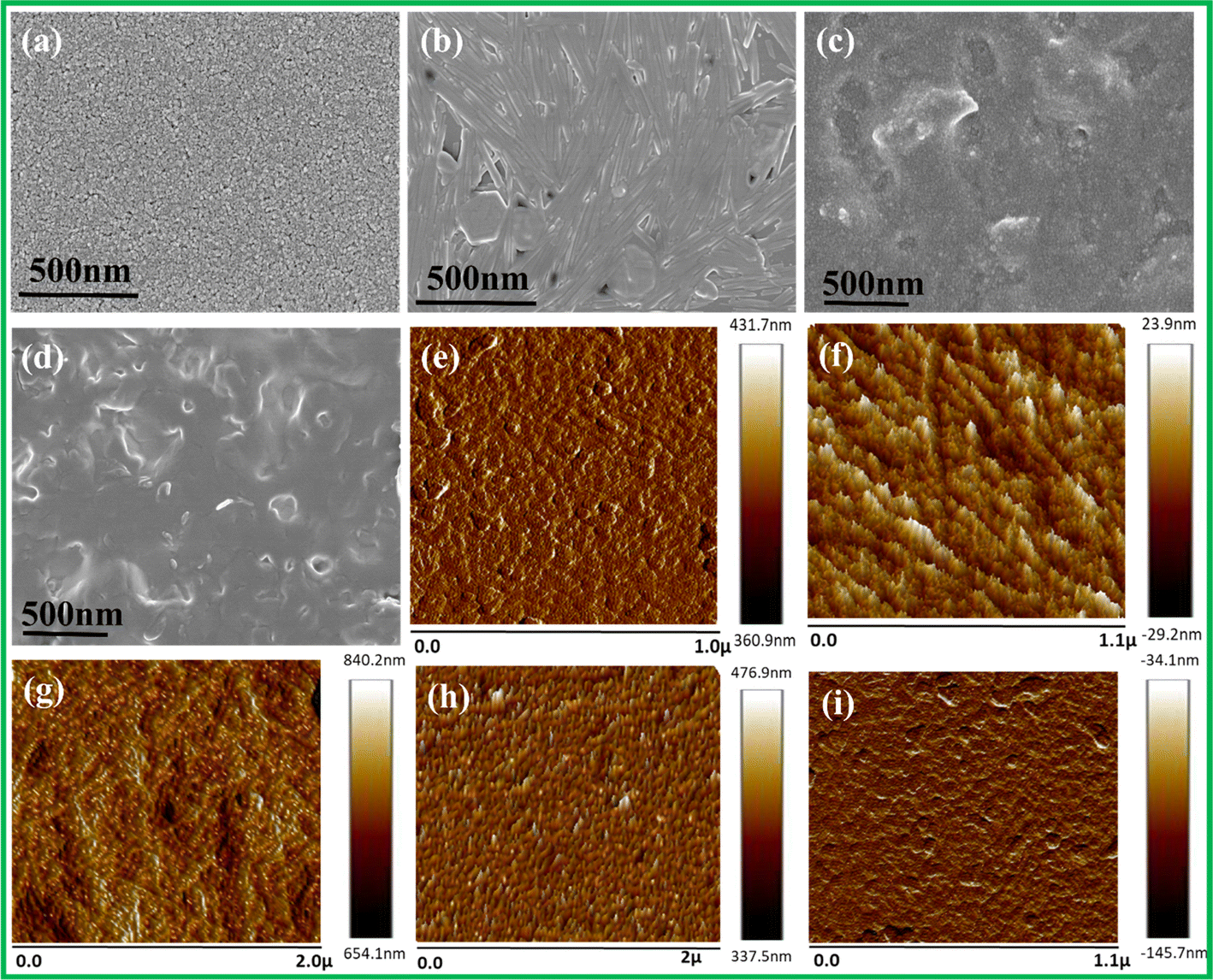 | ||
| Fig. 2 SEM images of the pristine PbSe QD film (a), CsPbI3 NR film (b), ZnO NPs (c), and hybrid ZnO:Cs2CO3 nanocomposite film (d). AFM images of pristine PbSe QDs (e), CsPbI3 NRs (f) and their blended CsPbI3:PbSe nanocomposite film (g), pristine ZnO NPs (h), and physically blended ZnO:Cs2CO3 nanocomposites (i). | ||
Photoluminescence (PL) intensity and lifetime are key parameters that can provide insights into the optical properties and carrier dynamics of materials. Fig. S7a† shows the PL of the pristine CsPbI3 and CsPbI3:PbSe composite. In the case of CsPbI3, its pristine form typically exhibits a strong PL signal due to its direct bandgap characteristics. The PL intensity and lifetime of CsPbI3 can be affected by factors such as defects, surface states, and interactions with other materials. In the CsPbI3:PbSe nanocomposite, the PL properties of CsPbI3 are expected to be influenced by the presence of PbSe QDs. The interaction between CsPbI3 and PbSe QDs can lead to changes in the PL intensity and lifetime of CsPbI3. For example, if the PbSe QDs act as recombination centers or quenchers, they could reduce the PL intensity and shorten the PL lifetime of CsPbI3. On the other hand, if the PbSe QDs facilitate charge transfer processes or passivate surface defects, they could enhance the PL intensity and prolong the PL lifetime of CsPbI3. As for the photoluminescence of PbSe QDs, they are known to exhibit size-dependent PL properties due to quantum confinement effects. Smaller PbSe QDs typically have higher PL quantum yields and shorter PL lifetimes compared to larger QDs. The PL of PbSe QDs can also be influenced by surface ligands, defects, and interactions with other materials in a composite structure. As shown in Fig. 3a, the PL intensity of the nanocomposites is increased and becomes broadened, which means the surface of the active layer is passivated and there is a strong increment of photo-induced charge carriers which can increase the exciton generation rates.
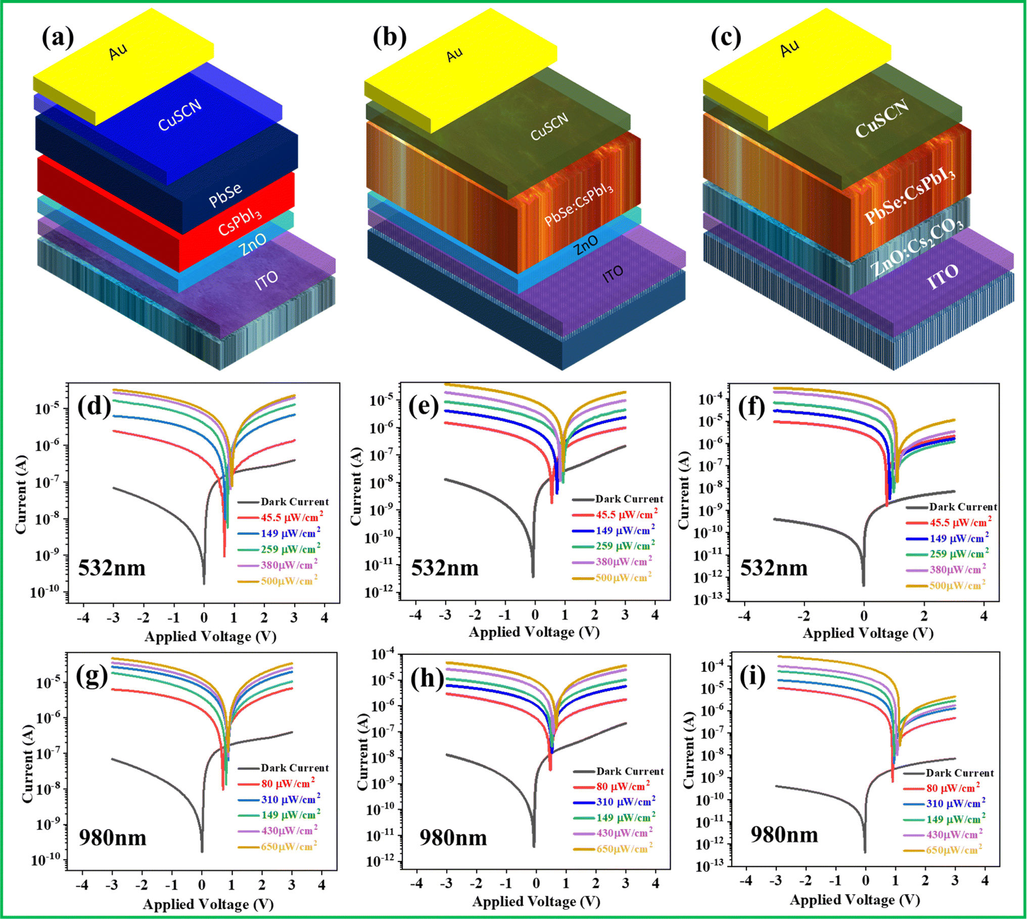 | ||
| Fig. 3 Schematic diagram of devices A (a), B (b), and C (c). I–V characteristics of fabricated devices A, B and C in the dark and under 532 nm (d–f) and under 980 nm (g–i) illumination. | ||
The carrier lifetime was evaluated using time-resolved photoluminescence (TRPL) spectroscopy with the time-correlated single-photon counting (TCSPC) method. This technique was employed for both pristine CsPbI3 NRs and CsPbI3:PbSe blended nanocomposites, utilizing an Edinburgh FLS920 system and a 405 nm laser. A 600 nm short-pass filter was applied to capture the emitted PL photons, as illustrated in Fig. S7b.† The higher normalized PL intensity observed in the blended nanocomposites indicates a higher presence of photo-induced charges in the blended film and a larger generation of excitons compared to pristine CsPbI3 NRs. The TRPL data was analyzed using bi-exponential fitting to extract the fast and slow decay components, denoted as τ1 and τ2, respectively. The fast PL decay (τ1) corresponds to non-radiative recombination caused by charge trapping effects. On the other hand, the slow decay rate (τ2) is associated with holes that are mostly localized in the core, while electrons are significantly localized at the surface. To calculate the average lifetimes (τave), the following relation was utilized: A(t) = A1exp(−t/τ1) + A2 exp(−t/τ2) and τave = (A1τ12 + A2τ22)/(A1τ1 + A2τ2). The parameters for CsPbI3 and CsPbI3:PbSe extracted from TRPL data after fitting are listed in Table S1 (in the ESI).† The reduced wave function overlap between the hole and electron of an exciton increases the radiative lifetime of the exciton. In the CsPbI3:PbSe nanocomposite, τ1 is higher than in pristine CsPbI3 NRs, indicating enhanced delocalization. This reduces charge trapping and non-radiative recombination and enhances the dissociation of photogenerated charge carriers, ultimately leading to improved device performance.
The incorporation of Cs2CO3 into the ZnO layer brings about a series of benefits that collectively contribute to the enhanced device performance.33,34 One key advantage is the improvement of electron transport properties within the ETL. ZnO nanoparticles possess excellent electron mobility, facilitating efficient electron extraction and transport. By blending Cs2CO3, additional charge carriers, including electrons, are introduced into the ZnO layer. This increased electron density results in improved electron mobility, reducing the likelihood of electron traps and enhancing the overall electron transport efficiency within the layer and can impact its charge transporting properties, interface interactions, and overall device performance. Therefore, the morphological characteristics revealed by the SEM images of these materials provide important insights into their potential roles in optoelectronic devices. The controlled synthesis and morphology of these materials contribute to their charge generation, transport, and interaction with incident light, ultimately influencing the efficiency and performance of photodetectors and other optoelectronic applications. The incorporation of the Cs2CO3 solution into the ZnO nanocrystal film aims to improve the device performance by modifying the electron transport properties.33,34
The current–voltage (I–V) curves of self-powered photodetectors provide valuable insights into their ability to generate photocurrent without an external bias. Three kinds of device structures have been fabricated to analyze the I–V curves: ITO/ZnO/CsPbI3/PbSe/CuSCN/Au (device A), ITO/ZnO/CsPbI3:PbSe/CuSCN/Au (device B), and ITO/ZnO:Cs2CO3/CsPbI3:PbSe/CuSCN/Au (device C), as shown in Fig. 3a–c, respectively. All these photodetectors offer important information about their photoresponse and self-driven behavior. The I–V curves of devices A, B, and C in the dark and under 532 nm illumination are shown in Fig. 3d–f, and those in the dark and under 980 nm illumination are shown in Fig. 3g–i. The dark current passes through the origin and the photocurrent shows a slight upward shift from the origin, indicating the self-driven behavior of the device. This deviation of the photocurrent from the dark current curve represents the self-generated photocurrent in all three kinds of structures due to the absorption of photons by the active layer and the heterojunction structures of the three photodetectors. Analysis of the I–V curves of all these self-powered photodetectors provides insights into their ability to generate photocurrent under illumination without an external bias.
Fig. 4a shows the dark current and photocurrents of the above three photodetectors to compare the difference of the device performances. As is well-established, achieving high-performance photodetectors necessitates a dual objective: minimizing the dark current while maximizing photocurrent. Consequently, the superior performance of device B to that of device A can be attributed to several factors: one is the formation of a bulk-heterojunction within the active CsPbI3:PbSe layer. In device B, the significant reduction of dark current can be attributed to the advantageous characteristics of the CsPbI3:PbSe bulk-heterojunction.
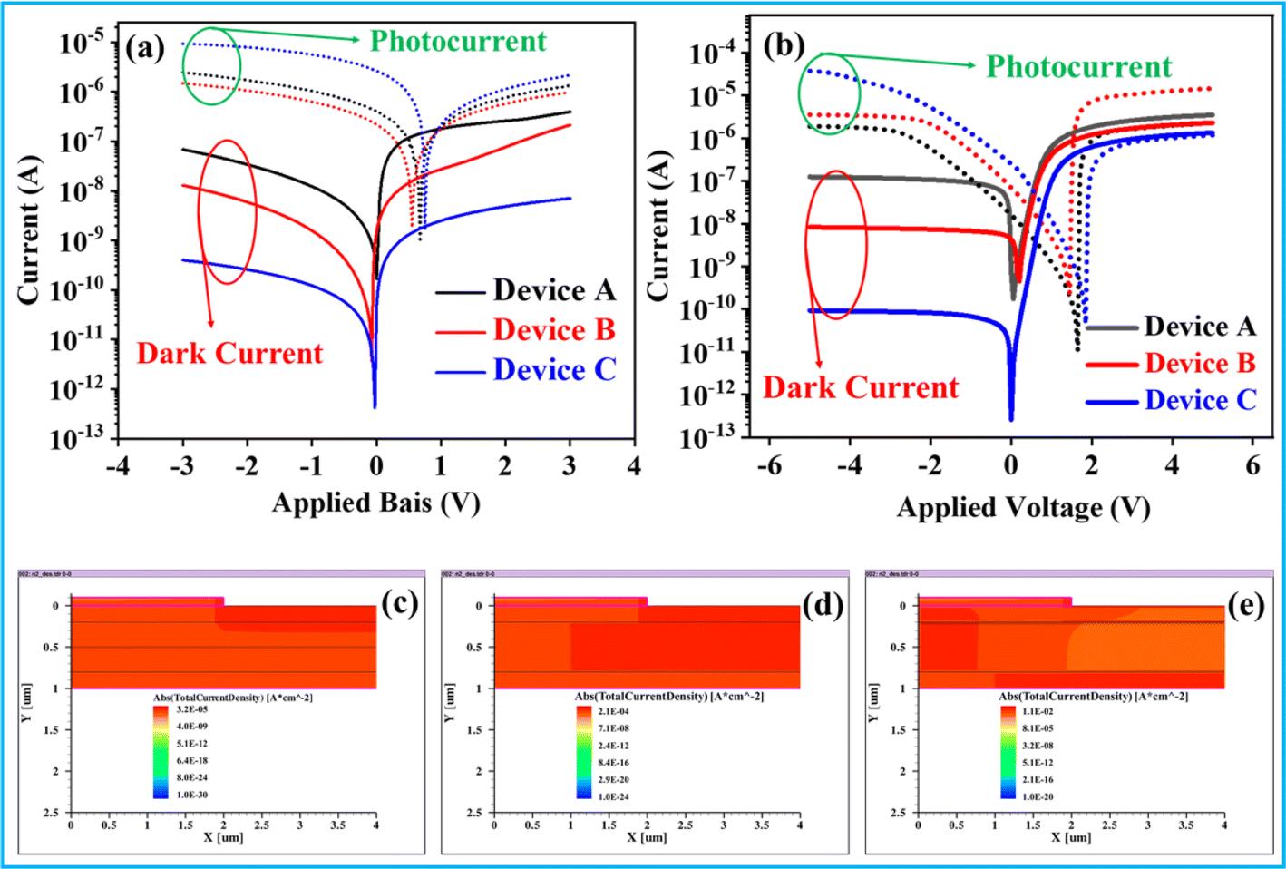 | ||
| Fig. 4 I–V curves of devices A, B and C in the dark and under 980 nm illumination (a), the simulated I–V characteristics of devices A, B and C in the dark and under 980 nm illumination (b), and the simulated photocurrent density maps for devices A (c), B (d) and C (e) under 980 nm illumination. | ||
The effective blending of these materials facilitates improved charge carrier separation and transport within the device. This, in turn, leads to a reduction in dark current levels. It should also be noted that the high performance of device B is not exclusively due to the lower dark current, but it's also associated with an amplified photocurrent. The bulk-heterojunction structure in this device enhances the absorption of incident photons and, consequently, the efficient generation and separation of charge carriers in response to illumination. However, unfortunately the photocurrent is not increased as expected; instead, it is less than that from device A. To understand why this happens, we should keep in mind that for the best photodetectors all the photons should produce excitons and all the excitons should be dissociated and then electrons and holes should be transported towards their respective electrodes. However, the possibility of carrier recombination in the bulk-heterojunction layer is higher than carrier dissociation due to the slow transportation of photogenerated electrons. Therefore, to improve the carrier transportation the electron transporting layer of ZnO is modified by blending it with Cs2CO3. Consequently, the dark current is further reduced and the photocurrent is further enhanced, as shown in Fig. 4a, due to efficient photogenerated electron extraction and transportation after their successful dissociation. Thus, one can see why device C shows the lowest dark current and the highest photocurrent as compared to the other two devices. A higher self-powered photoresponse implies more efficient charge carrier generation, separation, and collection within the active layer. Lower dark currents contribute to improved signal-to-noise ratios and enhanced self-powered performance.
The I–V curves of the self-driven photodetector ITO/ZnO:Cs2CO3/CsPbI3:PbSe/CuSCN/Au reveal its self-powered behavior and efficiency. The blended ZnO:Cs2CO3 layer contributes to the efficient extraction and transportation of photogenerated current from the CsPbI3:PbSe active layer. The deviation from the dark current curve highlights the enhanced charge carrier dynamics introduced by the modification of the photoactive layer and ETL. This self-powered response shows the potential of the device to operate at zero bias, converting the incident light into usable electrical current. Additionally, the performances of the photodetectors were examined by theoretical simulation in terms of dark current and photocurrent to verify their reliability. Fig. 4b shows the I–V curves in the dark and under illumination for devices A, B, and C, which are extracted from their J–V maps of photocurrents in Fig. 4c–e, respectively. From these I–V results one can see that the simulated results are very consistent with experimental data, verifying the reliability of the device.
To comprehensively evaluate the photoelectric performance of the device, we conducted measurements on the crucial figure of merit parameters of photodetectors. Because device C shows the best performance among these devices, the following calculations are presented only for device C. Fig. 5a presents the dependence of photocurrent on the incident illumination intensity in the self-driven mode. Clearly, the photocurrent increases with increasing the incident intensity. Upon further increasing the illumination intensity, a saturation point is reached, indicating the expansion of the depletion region due to the excess carriers at the heterojunction. An essential attribute of the photodetector, photosensitivity (K), was evaluated. This parameter represents the ratio of incident light spanning a broad spectral range to the dark current, and it is mathematically expressed as K = Iphoto/Idark.27–29 Here, Iphoto corresponds to the current under illumination (Iill − Idark), where Iill represents the current under illumination and Idark represents the dark current. Notably, the photosensitivity value was determined to be 7.25 × 10⁴ under 80 μW cm−2 980 nm illumination. Similarly, Fig. 5b shows the photosensitivity of device C with respect to the incident light intensity. The sensitivity of a photodetector under illumination is termed as photoresponsivity (R), and it is expressed as R = Iphoto/Pill,35,36 representing the ratio of the photocurrent to the illumination power intensity (Pill). It is noteworthy that peak R of device C, which is 9.29 A W−1 under 80 μW cm−2 980 nm illumination, is depicted in Fig. 5c. It is evident that R declines with increasing the illumination. The specific detectivity (D*), which is dependent upon R and dark current, was determined by the relationship  , where q is the electronic charge, R is the photoresponsivity, and A is the effective area of the conductive channel within the photodetector.37,38Fig. 5d provides insight into D* as a function of illumination intensity. It is essential to acknowledge that the value of D* is intricately linked to R and the dark current. Consequently, higher D* values are achieved through elevated photoresponsivity and suppressed dark current. Remarkably, a substantial D* of 3.17 × 10¹⁴ Jones is recorded under an illumination of 80 μW cm−2 at 0 V. This pronounced enhancement in photoresponse corroborates efficient electron dissociation through the bulk-heterojunction mechanism, where both region surfaces (photoactive layer and electron-transporting layer) are passivated. Electrons and holes are adeptly mobilized by the ZnO:Cs2CO3 and CuSCN components, and subsequently extracted through extended buffer layers. Photoelectric parameters as a function of illumination intensity for devices A and B are shown in Fig. S8 and S9,† respectively. The R and D* under 532 and 980 nm illumination are shown in Fig. 6. From here, an extensive analysis was carried out to thoroughly assess the photoresponsivity and specific detectivity of devices A, B, and C. This comprehensive evaluation aimed to facilitate a comprehensive comparison among all devices, encompassing various levels of illumination intensity.
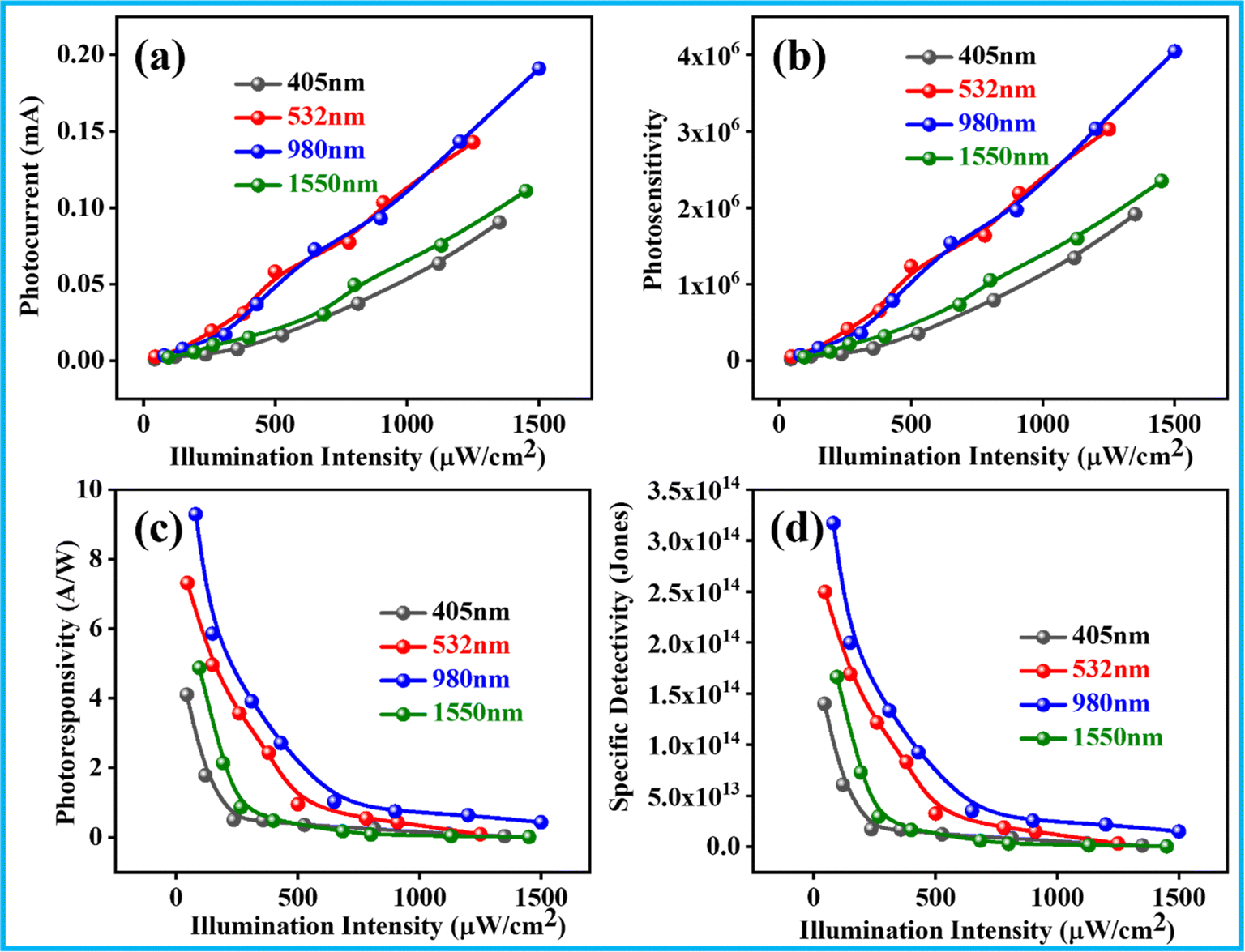 | ||
| Fig. 5 Photoelectric performance of the ITO/ZnO:Cs2CO3/CsPbI3:PbSe/CuSCN/Au photodetector (device C). The photocurrent (a), photosensitivity (b), photoresponsivity (R) (c), and specific detectivity (D*) (d) vs. illumination intensity in the self-driven mode under 405 nm, 532 nm, 980 nm, and 1550 nm illumination. | ||
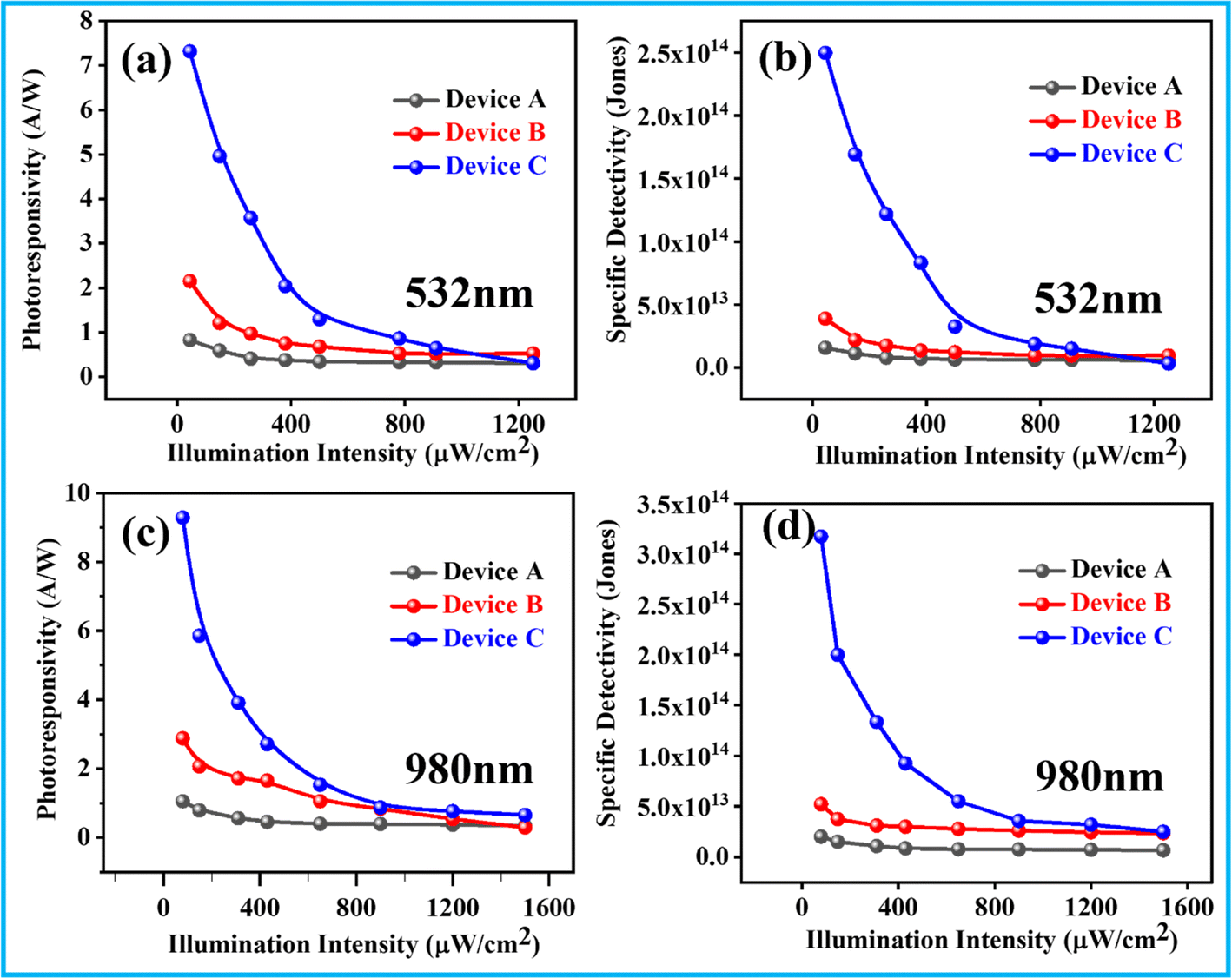 | ||
| Fig. 6 Photoresponsivity and specific detectivity of devices A, B and C under 532 nm (a and b) and 980 nm (c and d) illumination with different intensities. | ||
The linear dynamic range (LDR) is a crucial parameter that characterizes photodetectors, indicating their capability to accurately detect a broad spectrum of light intensities. It quantitatively assesses the photodetector's ability to maintain linearity in its response across a wide range of incident light intensities, thereby highlighting its sensitivity and versatility in capturing different light levels. This metric is defined as 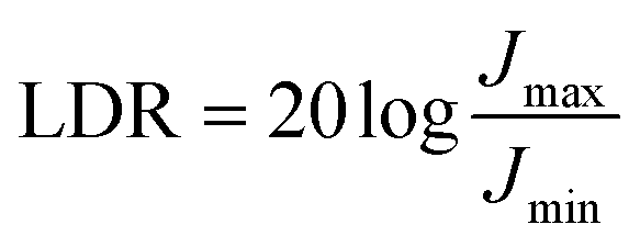 , where Jmax and Jmin denote the maximum and minimum measurable current densities, respectively.39 For the case of device C, a substantial LDR value of 80 dB is achieved under 80 μW cm−2 980 nm illumination. This remarkable LDR value underscores the device's capacity to accommodate a diverse spectrum of light intensities while maintaining accurate and reliable performance. The high LDR value of device C emphasizes its potential suitability for applications with superior precision across a broad range of light levels. Fig. S10† shows the illumination intensity dependent LDR for devices A (a), B (b), and C (c) under 405 nm, 532 nm, 980 nm, and 1550 nm illumination, respectively. Furthermore, Table S2† (in the ESI) shows a comprehensive compilation of the essential parameters associated with devices A, B and C. Notably, the device performance is not only on par with but in some cases even superior to those of previously reported self-driven photodetectors. Thus, the advancement achieved by the current study in enhancing the performance and efficiency of self-driven photodetectors thereby contributes to the progression of photodetection technologies. A comparative analysis of current device performances with existing literature to demonstrate the advancements and unique features of photodetector devices is presented in Table S3†, which provides a comprehensive comparison of previously presented self-powered photodetectors based on perovskites and other nanomaterials.
In the context of applications such as switching and high-frequency optical sensing, an investigation into the time-dependent photoresponse behavior of the photodetectors was conducted, encompassing diverse laser wavelengths and various illumination intensities. Fig. 7a and c show the time-dependent photoresponse characteristics of device C under a specific illumination intensity, at 0 V and −3 V. Simultaneously, Fig. 7b and d show the time-dependent photoresponse of device C at 0 V under various illumination intensities. The outcomes of these experiments highlight the facile transition between ON/OFF modes in the context of broadband detection for device C, confirming its reproducibility. The rising time (τr) and falling time (τf), denoting the time interval for the photocurrent to ascend from 10% to 90% and descend from 90% to 10%, respectively, were calculated as per established practice.40 The specific values of τr and τf are comprehensively displayed in Fig. S11–S13 (in the ESI),† providing a comprehensive overview of the temporal characteristics of the photodetector's photoresponse.
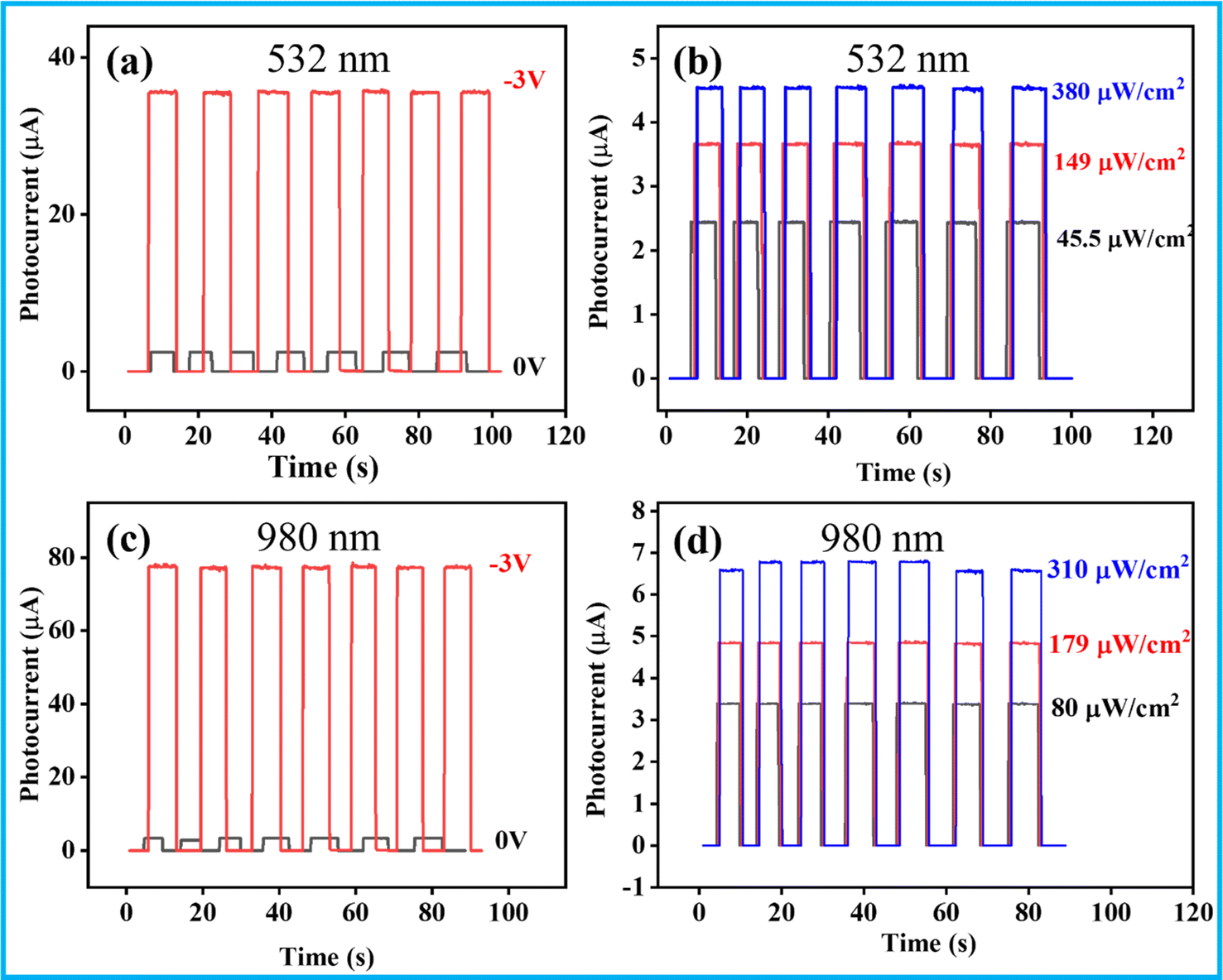 | ||
| Fig. 7 Time-dependent photoresponse of the self-driven photodetector (device C) at 0 V and −3 V under 532 nm (a and b) and 980 nm (c and d) illumination with fixed and under various intensities. | ||
The examination of device performance is extended through the utilization of theoretical simulations, wherein a comprehensive analysis is conducted encompassing several crucial parameters for devices A, B and C. These simulations entail the estimation of absorbed photon density, exciton generation, electron density, electron mobility, and the determination of built-in electrostatic potential, all of which are facilitated through TCAD simulations. Fig. 8a–c exhibit the spatial distribution maps of absorbed photon density, exciton generation, and electron density within device A. Correspondingly, Fig. 8d–f illustrate the corresponding absorbed photon density, optical generation, and electron density maps for device B, while Fig. 8g–i show the same for device C. The estimation of photon-absorbed density within the photoactive region of the device across distinct wavelengths can be facilitated through simulation, providing insights into the photon interaction dynamics. Remarkably, the simulation revealed a peak photon-absorbed density of 5.9 × 1020 cm−3 s−1 under 980 nm illumination. Notably, upon a comparative evaluation of these maps, it becomes evident that device C outperforms devices A and B in terms of their exhibited characteristics, which is in good agreement with experimental results. These comprehensive visualizations offer insights into the localized behavior and interaction of critical parameters within the distinct active regions of the device. Such analyses contribute to a deep understanding of the mechanisms underpinning the performance differences for all devices, aiding in the identification of factors contributing to the superior performance of device C. The photon absorbed densities across a range of wavelengths, namely 405 nm, 532 nm, 980 nm, and 1550 nm, are illustrated in Fig. S14.† The proficiency of the hybrid nanocomposite in eliciting exciton generation within the active region hinges upon its absorption capacity. This correlation is appropriately illustrated through the exciton generation maps shown in Fig. 8, substantiating the congruence between absorbed photon densities and exciton generation patterns. Consequently, the augmented exciton generation count in the active region, facilitated by the hybrid CsPbI3:PbSe nanocomposite, engenders a concurrent enhancement in photocurrent. Further insight into the system's behavior is garnered from the maximum electron density at the active layer's surface, which is deduced to be 8.5 × 1017 cm−3 in the simulated device C, as depicted in Fig. 8. This parameter offers valuable knowledge about the concentration of charge carriers and their interaction within the photoactive layer. Additionally, the simulation investigates the determination of built-in potentials for the devices, which is a critical parameter that supports the operational characteristics of the device. These approximations of built-in potential for devices A, B and C are presented in Fig. 9a–c, providing insights into the interplay of electronic charge distributions and their effects on the built-in potentials. Collectively, the simulation-derived information concerning photon-absorbed density, exciton generation, electron density, and built-in potentials contributes to a comprehensive understanding of the device's optoelectronic performance and establishes crucial insights into the factors governing its operation. The stability of device C is shown in Fig. S15 and S16† following a 60 day period. The aim of this experiment is to evaluate the dark and photocurrent characteristics as well as the time-dependent photoresponse of the manufactured photodetector in order to determine its reliability. In order to assess any changes in performance over time, measurements were performed both on the first day and sixty days thereafter. The findings show that the device performance decreased by 3% from its initial state to the end of the 60 day period. The apparatus maintains its self-powered behavior in spite of this modest decline, highlighting its steady and dependable operation over a prolonged length of time.
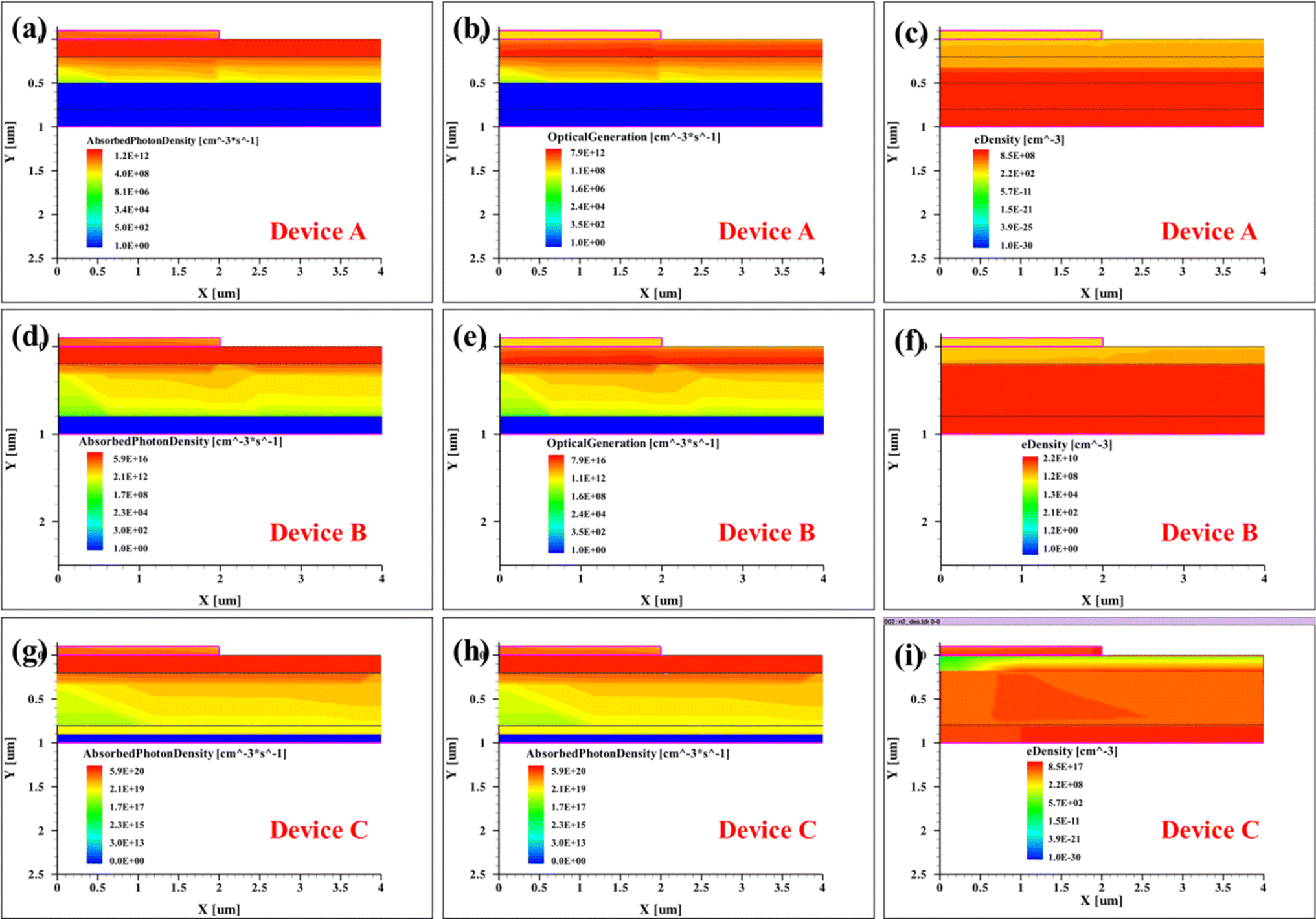 | ||
| Fig. 8 Simulated absorbed photon density, exciton generation and electron mobilities for devices A (a–c), B (d–f) and C (g–i) under 980 nm illumination. | ||
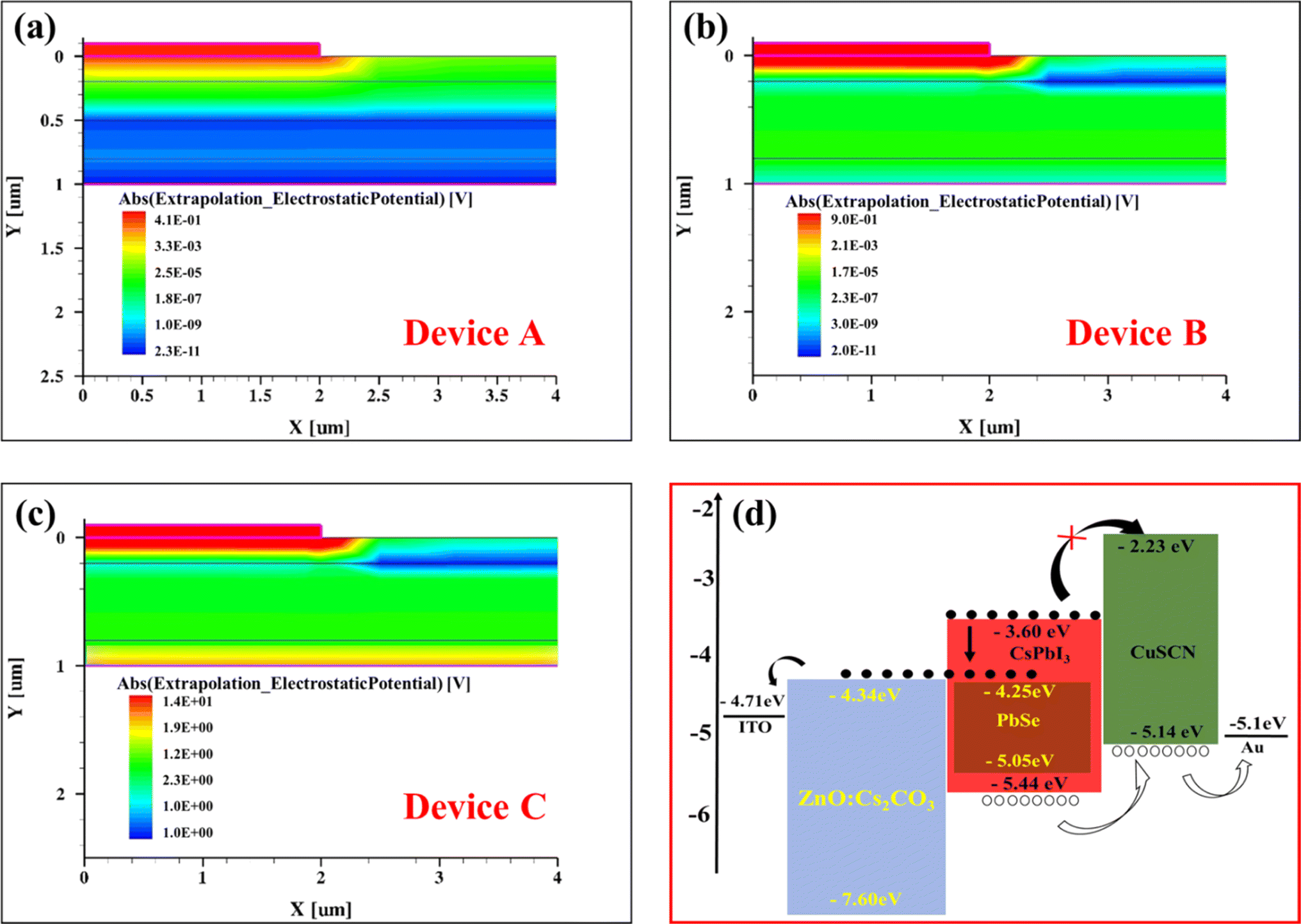 | ||
| Fig. 9 Built-in electrostatic potential maps for Device 1 (a), Device 2 (b), and Device 3 (c) by using TCAD simulation. Schematic diagram for estimating the energy levels to understand the electron transportation mechanism (d). | ||
Clarifying the underlying mechanism of photocurrent generation assumes essential significance. In the context of achieving high-performance photodetectors, key factors encompass the attenuation of dark current and the augmentation of photocurrent. The origin of dark current predominantly traces back to the rate of charge injection from the electrodes into the active layer, where this injection rate finds its grounding in the injection barrier. The process involves the injection of carriers from a high work function electrode into the lowest unoccupied molecular orbital (LUMO) energy level or thermally generated carriers within the active layer. These carriers then navigate under applied voltages towards their respective electrodes, eventually converging at the electrode interface. Minimization of the hole injection barrier is feasible by selecting an electrode with a lower work function, entailing a deeper highest occupied molecular orbital (HOMO) energy layer. Consequently, the stratification of the photoactive layer warrants meticulous calibration to realize a reduced dark current and magnified photocurrent.
The incorporation of CsPbI3:PbSe engenders a partial donor–acceptor interpenetration due to the coexistent physically blended bulk heterojunction, fostering a pristine phase capable of efficaciously obstructing adverse charge carriers during periods of darkness and intensifying photocurrent upon illumination. Under specific wavelength illumination, electron promotion from the HOMO to LUMO transpires. CuSCN and ZnO:Cs2CO3 assume crucial roles in further curtailing dark current and amplifying photocurrent through the imposition of higher energy barriers. These layers, besides serving as hole-transporting and electron-transporting agents, concurrently function as electron-blocking and hole-blocking layers, respectively. This multi-faceted deployment of CuSCN and ZnO:Cs2CO3 engenders augmented energy barriers for charge injection during reverse bias, while sustaining an intricate energy cascade bridging the CsPbI3:PbSe layer and the associated electrodes. Fig. 9 shows the estimated energy-band diagram for device C to understand the underlying mechanism of photogenerated electrons and their transportation after exciton dissociation. The HOMO and LUMO levels for PbSe, CsPbI3, ZnO, and ZnO:Cs2CO3 presented in the energy band diagram are estimated by ultraviolet photoelectron spectroscopy (UPS) measurement and the extrapolation of Tauc plots extracted from the absorption spectra. The efficient generation of charge carriers and the reduction of non-radiative recombination contribute to the improved photoresponsivity and overall device performance. The use of a blended ZnO:Cs2CO3 as an ETL also offers the potential for spectral tuning in optoelectronic devices. The bandgap of ZnO nanoparticles is well suited for UV absorption, whereas the optical transparency of Cs2CO3 in the UV region allows for effective light transmission. By adjusting the blending ratio between ZnO and Cs2CO3, it may be possible to fine-tune the absorption properties of the ETL, optimizing its response to specific wavelength ranges. This tunability could lead to the development of devices with tailored spectral sensitivity, addressing specific application requirements.
The transportation of charge carriers within the uniform and passivated photoactive layer (CsPbI3:PbSe) and the ETL composed of a ZnO:Cs2CO3 nanocomposite film is governed by the injected charge carriers and their mobility. Additionally, the activation energy and injection barrier for hole mobility can be decoupled in semiconductor devices.41 Consequently, defects present on the surface of the active layer can reduce the thermal activation energy within the pristine CsPbI3 layer. The interpenetration of PbSe QDs with CsPbI3 NRs may create a conducting channel due to the passivation effects. Similarly, the interpenetration of ZnO into Cs2CO3 can establish a compact n-type conducting channel as the ETL at the bottom, connected to the photoactive region. This configuration reduces the total resistance by facilitating efficient charge transport through the active layer. Enhanced electron mobility in the hybrid films and their accelerated movement towards the respective electrodes emphasize rapid carrier transport through the bulk heterojunction. In essence, the photodetectors' operation hinges on exciton creation in the active region via photon absorption within the passivated compact film. Subsequent dissociation of these excitons into electrons and holes at both interfaces of the active layer will be enhanced. These disassociated charge carriers are then collected by their respective electrodes via the electron-transporting and hole-transporting layers and then transported towards their respective electrodes. However, achieving enhanced carrier transport presents challenges despite the apparent simplicity of the setup. Firstly, photogenerated excitons must reach the interfaces to avoid recombination. Secondly, favorable energy level positions at the interface promote swift exciton dissociation. The primary goal is to maximize the number of charge carriers under illumination by minimizing recombination within the active region. Consequently, carrier dissociation rates and their transport can be maximized. Therefore, the integration of ZnO with Cs2CO3 modifies the ETL, decreases the recombination and enhances the separation of charge carriers generated by light absorption. These outcomes highlight the reliability and precision of the photodetectors for diverse self-driven sensing applications. Similarly, an enhanced photoresponse can be achieved through further optimization of the device configuration, capitalizing on the synergistic optoelectronic properties facilitated by the CsPbI3:PbSe nanocomposite and surface-passivated ZnO:Cs2CO3 ETL. Consequently, a broader range of applications can be predicted for innovative photonic and optoelectronic devices.
4. Conclusion
In summary, in this work we have comprehensively explored the design, fabrication, and performance evaluation of self-driven photodetectors based on a novel configuration comprising CsPbI3:PbSe nanocomposites and ZnO:Cs2CO3 electron-transporting layers. Through a systematic analysis of various material characterizations and device measurements, significant enhancements in both dark current reduction and photocurrent amplification were achieved. The integration of Cs2CO3 with ZnO as the ETL effectively improved charge carrier transportation, leading to increased separation and reduced recombination of photogenerated carriers within the active layer. This was evidenced by the higher photosensitivity, photoresponsivity, and specific detectivity of 7.25 × 10⁴, 9.29 A W−1, and 3.17 × 10¹⁴ Jones demonstrated by the photodetector ITO/ZnO:Cs2CO3/CsPbI3:PbSe/CuSCN/Au under 80 μW cm−2 980 nm illumination in the self-driven mode. Theoretical simulations provided insights into the underlying mechanisms and corroborated the experimental data. The devices were found to be self-driven, as seen by the notable increase in photocurrent when compared to the dark current. This shift was attributed to efficient charge separation in both the experimental and theoretically computed results. Our comprehension of the functions of different parts of the device design is improved by these discoveries, which also create new opportunities for the creation of high-performance self-driven photodetectors with a wider range of optoelectronic device applications.Author contributions
In this collaborative research endeavor, the authors made distinct and valuable contributions to the manuscript. Muhammad Sulaman played a pivotal role in crafting the original draft, undertaking data acquisition, and contributing to the methodological aspects of the study. Shengyi Yang, as a supervisor, provided oversight, engaged in thorough review and editing, and secured funding for the project. The formal analysis and review contributions were skillfully executed by Honglian Guo and Chuanbo Li. Ali Imran contributed to the methodology, while Arfan Bukhtiar handled software and visualization aspects. Muhammad Qasim and Zhenhua Ge made significant contributions to software and methodology. Yong Song conducted formal analysis, and Yurong Jiang contributed to the review and editing process. Lastly, Bingsuo Zou played a critical role in acquiring funding for the research.Conflicts of interest
There are no conflicts to declare.Acknowledgements
This work was partially funded by the projects of the Key R & D projects of the Ministry of Science and Technology of China (SQ2019YFB220038), the National Natural Science Foundation of China (No. 1227041254, 52350410471, and 62274190), the International Collaboration Project of Ministry of Science and Technology (Grant No. G2022184006L), the Fundamental Research Funds for the Central Universities (No.2020CX02002 and BITBLR2020013), the open foundation of Guangxi Key Laboratory of Processing for Non-ferrous Metals and Featured Materials, Guangxi University (Grant No. 2021GXYSOF18), and Bagui Scholar Fund of Guangxi province.References
- S. Sahare, P. Ghoderao, M. K. Sharma, M. Solovan, R. Aepuru, M. Kumar, Y. Chan, M. Ziółek, S. L. Lee and Z. H. Lin, Pyro-phototronic effect: An effective route toward self-powered photodetection, Nano Energy, 2023, 107, 108172 CrossRef CAS.
- L. Su, W. Yang, J. Cai, H. Chen and X. Fang, Self-Powered Ultraviolet Photodetectors Driven by Built-In Electric Field, Small, 2017, 13, 1701687 CrossRef PubMed.
- C. P. Veeramali, S. Y. Yang, R. Zhi, M. Sulaman, M. I. Saleem, Y. Cui, Y. Tang, Y. R. Jiang, L. Tang and B. S. Zou, Solution-Processed, Self-Powered Broadband CH3NH3PbI3 Photodetectors Driven by Asymmetric Electrodes, Adv. Opt. Mater., 2020, 8, 2000215 CrossRef.
- X. Gan and D. Lei, Plasmonic-metal/2D-Semiconductor Hybrids for Photodetection and Photocatalysis in Energy-Related and Environmental Processes, Coord. Chem. Rev., 2022, 469, 214665 CrossRef CAS.
- S. Shafique, S. Yang, T. Iqbal, B. Cheng, Y. Wang, H. Sarwar, Y. T. Woldu and P. Ji, Improving the performance of V2O5/rGO hybrid nanocomposites for photodetector applications, Sens. Actuators, A, 2021, 332, 113073 CrossRef CAS.
- G. Konstantatos and E. H. Sargent, Nanostructured materials for photon detection, Nat. Nanotechnol., 2010, 5, 391–400 CrossRef CAS PubMed.
- S. Pal, A. Ghorai, S. Mahato and S. K. Ray, Piezo-Phototronic Effect-Induced Self-Powered Broadband Photodetectors using Environmentally Stable α-CsPbI3 Perovskite Nanocrystals, Adv. Opt. Mater., 2023, 11, 2300233 CrossRef CAS.
- M. Sulaman, S. Y. Yang, A. Bukhtiar, P. Tang, Z. H. Zhang, Y. Song, A. Imran, Y. R. Jiang, Y. Cui, L. Tang and B. S. Zou, Hybrid Bulk-Heterojunction of Colloidal Quantum Dots and Mixed-Halide Perovskite Nanocrystals for High-Performance Self-Powered Broadband Photodetectors, Adv. Funct. Mater., 2022, 32, 2201527 CrossRef CAS.
- X. Zhou, X. Hu, S. Zhou, H. Song, Q. Zhang, L. Pi, L. Li, H. Li, J. Lv and T. Zhai, Tunneling diode based on WSe2/SnS2 heterostructure incorporating high detectivity and responsivity, Adv. Mater., 2018, 30, 1703286 CrossRef PubMed.
- M. Sulaman, S. Y. Yang, Y. Song, A. Bukhtiar, J. M. Hu, Z. Zhang, Y. R. Jiang, Y. Cui, L. Tang and B. S. Zou, Hybrid Nanocomposites of All-Inorganic Halide Perovskites with Polymers for High-Performance Field-Effect-Transistor-based Photodetectors: An Experimental and Simulation Study, Adv. Mater. Interfaces, 2022, 9, 2200017 CrossRef CAS.
- M. Sulaman, S. Y. Yang, Z. Zhang, A. Imran, A. Bukhtiar, Z. Ge, Y. Tang, Y. Jiang, L. Tang and B. S. Zou, Lead-free Tin-based Perovskites Nanocrystals for High-Performance Self-driven Bulk-Heterojunction Photodetectors, Mater. Today Phys., 2022, 27, 100829 CrossRef CAS.
- W. C. Huang, Y. H. Lin and Y. H. Zhang, et al., Investigation of ZnO/V2O5 hybrid nanocomposite-based ultraviolet photodetector and hydrogen gas sensor, J. Mater. Sci.: Mater. Electron., 2023, 34, 398 CrossRef CAS.
- J. R. Wen, F. Alberto, R. Ortiz, A. Champ and M. T. Sheldon, Kinetic Control for Continuously Tunable Lattice Parameters, Size, and Composition during CsPbX3 (X = Cl, Br, I) Nanorod Synthesis, ACS Nano, 2022, 16(5), 8318–8328 CrossRef CAS PubMed.
- X. Song, Y. Jian, X. Wang, J. Chen, Q. Shan, S. Zhang, Z. Chen, X. Chen and H. Zeng, Hybrid mixed-dimensional WTe2/CsPbI3 perovskite heterojunction for high-performance photodetectors, Nanotechnology, 2023, 34, 195201 CrossRef PubMed.
- N. Ding, Y. Wu, W. Xu, L. Zi, L. Shao, R. Sun, N. Wang, S. Liu, D. Zhou, X. Bai, J. Zhou and H. Song, A novel approach for designing efficient broadband photodetectors expanding from deep ultraviolet to near infrared, Light: Sci. Appl., 2022, 11, 91 CrossRef CAS PubMed.
- Y. Chen, Z. Feng, A. Pal and J. Zhang, Recent Progress on the Performance of Lead-Based Halide Perovskite APbX3 Detectors, Phys. Status Solidi A, 2022, 219, 2200018 CrossRef CAS.
- X. Ding, M. Cai, X. Liu, Y. Ding, X. Liu, Y. Wu, T. Hayat, A. Alsaedi and S. Dai, Enhancing the Phase Stability of Inorganic α-CsPbI3 by the Bication-Conjugated Organic Molecule for Efficient Perovskite Solar Cells, ACS Appl. Mater. Interfaces, 2019, 11(41), 37720–37725 CrossRef CAS PubMed.
- K. M. Sim, A. Swarnkar, A. Nag and D. S. Chung, Phase Stabilized α-CsPbI3 Perovskite Nanocrystals for Photodiode Applications, Laser Photonics Rev., 2018, 12, 1700209 CrossRef.
- M. I. Saleem, S. Y. Yang, A. Batool, M. Sulaman, C. P. Veeramalai, Y. Jiang, Y. Tang, Y. Y. Cui, L. Tang and B. S. Zou, CsPbI3, Nanorods as the Interfacial Layer for High-Performance, All-Solution-Processed Self-Powered Photodetectors, J. Mater. Sci. Technol., 2021, 75, 196–204 CrossRef CAS.
- M. Sulaman, S. Y. Yang, A. Bukhtiar, C. Fu, T. Song, H. Wang, Y. Wang, B. He, Y. Tang and B. S. Zou, High performance solution-processed infrared photodetector based on PbSe quantum dots doped with low carrier mobility polymer poly(N-vinylcarbazole), RSC Adv., 2016, 6, 44514–44521 RSC.
- C. J. Fu, H. W. Wang, T. J. Song, L. Zhang, W. L. Li, B. He, M. Sulaman, S. Y. Yang and B. S. Zou, Stability enhancement of PbSe quantum dots via post-synthetic ammonium chloride treatment for a high-performance infrared photodetector, Nanotechnology, 2015, 27(6), 65201 CrossRef PubMed.
- M. Sulaman, Y. Song, S. Y. Yang, M. Li, M. I. Saleem, P. V. Chandraseakar, Y. Jiang, Y. Cui, Q. Hao and B. S. Zou, Interlayer of PMMA doped with Au nanoparticles for high-performance tandem photodetectors: a solution to suppress dark current and maintain high photocurrent, ACS Appl. Mater. Interfaces, 2020, 12, 26153–26160 CrossRef CAS PubMed.
- J. M. Hu, S. Y. Yang, Z. Zhang, H. Li, P. V. Chandrasekar, M. Sulaman, M. I. Saleem, Y. Tang, Y. R. Jiang, L. Tang and B. S. Zou, Solution-processed, flexible and broadband photodetector based on CsPbBr3/PbSe quantum dot heterostructures, J. Mater. Sci. Technol., 2021, 68, 216–226 CrossRef CAS.
- S. J. Jeong, S. Cho, B. Moon, J. A. Teku, M. H. Jeong, S. Lee, Y. Kim and J. S. Lee, Zero Dimensional–Two Dimensional Hybrid Photodetectors Using Multilayer MoS2 and Lead Halide Perovskite Quantum Dots with a Tunable Bandgap, ACS Appl. Mater. Interfaces, 2023, 15(4), 5432–5438 CrossRef CAS PubMed.
- S. Wang, C. Bi, A. Portniagin A, J. Yuan, J. Ning, X. Xiao, X. Zhang, Y. Y. Li, S. V. Kershaw, J. Tian and A. L. Rogach, CsPbI3/PbSe heterostructured nanocrystals for high-efficiency solar cells, ACS Energy Lett., 2020, 5, 2401–2410 CrossRef CAS.
- D. He, M. Zeng, Z. Zhang, Y. Bai, G. Xing, H. M. Cheng and Y. Lin, Exciton diffusion and dissociation in organic and quantum-dot solar cells, SmartMat, 2023, 4, e1176, DOI:10.1002/smm2.1176.
- M. Vafaie, J. Z. Fan, A. M. Najarian, O. Ouellette, L. K. Sagar, K. Bertens, B. Sun, F. P. G. de Arquer and E. H. Sargent, Colloidal quantum dot photodetectors with 10-ns response time and 80% quantum efficiency at 1,550 nm, Matter, 2021, 4, 1042–1053 CrossRef CAS.
- Z. Cao, F. Zhang, J. Liu, C. Fan, Y. Wu and Y. Hao, Recent advances in encapsulation of highly stable perovskite nanocrystals and their potential applications in optoelectronic devices, Phys. Chem. Chem. Phys., 2023, 25, 17725–17736 RSC.
- S. Salari, M. Ahmadi and K. Mirabbaszadeh, Sol-Gel processed GZO thin film from low concentration solution and investigating GZO/Cs2CO3 bilayer, Electron. Mater. Lett., 2014, 10, 13–20 CrossRef CAS.
- J. Huang, G. Li, E. Wu, Q. Xu and Y. Yang, Achieving High-Efficiency Polymer White-Light-Emitting Devices, Adv. Mater., 2006, 18, 114–117 CrossRef CAS.
- M. Sulaman, S. Y. Yang, A. Imran, Z. Zhang, A. Bukhtiar, Z. Ge, Y. Song, F. Sun, Y. R. Jiang, L. Tang and B. S. Zou, Two Bulk-heterojunctions made of Blended Hybrid Nanocomposites for High-performance Broadband, Self-driven Photodetectors, ACS Appl. Mater. Interfaces, 2023, 15, 25671–25683 CrossRef CAS PubMed.
- L. Protesescu, S. Yakunin, M. I. Bodnarchuk, F. Krieg, R. Caputo, C. H. Hendon, R. X. Yang, A. Walsh and M. V. Kovalenko, Nanocrystals of Cesium Lead Halide Perovskites (CsPbX3, X = Cl, Br, and I): Novel Optoelectronic Materials Showing Bright Emission with Wide Color Gamut, Nano Lett., 2015, 15, 3692–3696 CrossRef CAS PubMed.
- G. Cheng, W. Y. Tong, K. H. Low and C. M. Che, Thermal-annealing-free inverted polymer solar cells using ZnO/Cs2CO3 bilayer as electron-selective layer, Sol. Energy Mater. Sol. Cells, 2012, 103, 164–170 CrossRef CAS.
- M. U. Hassan, Y. C. Liu, K. Hasan, H. Butt, J. F. Chang and R. H. Friend, Highly efficient PLEDs based on poly(9,9-dioctylfluorene) and Super Yellow blend with Cs2CO3 modified cathode, Appl. Mater. Today, 2015, 1, 45–51 CrossRef.
- M. Sulaman, S. Y. Yang, Y. R. Jiang, Y. Tang and B. S. Zou, Enhanced Performance of Solution-Processed Broadband Photodiodes by Epitaxially Blending MAPbBr3 Quantum Dots and Ternary PbSxSe1−x Quantum Dots as the Active Layer, Nanotechnology, 2017, 28, 505501 CrossRef PubMed.
- A. Imran, M. Sulaman, S. Y. Yang, A. Bukhtiar, M. Qasim, S. Elshahat, M. S. A. Khan, G. Dastgeer, B. S. Zou and M. Yousaf, Molecular Beam Epitaxy Growth of High Mobility InN Film for High-Performance Broadband Heterointerface, Surf. Interfaces, 2022, 29, 101772 CrossRef CAS.
- M. Sulaman, S. Y. Yang, T. Song, H. Wang, Y. Wang, B. He, D. Miao, Y. Tang, Y. Song and B. S. Zou, High performance solution-processed infrared photodiode based on ternary PbSxSe1−x colloidal quantum dots, RSC Adv., 2016, 6, 87730–87737 RSC.
- M. Sulaman, Y. Song, S. Y. Yang, M. Li, M. I. Saleem, P. V. Chandraseakar, Y. Jiang, Y. Tang and B. S. Zou, Ultra-sensitive solution-processed broadband photodetectors based on vertical field-effect transistor, Nanotechnology, 2020, 31, 105203 CrossRef CAS PubMed.
- M. Sulaman, Y. Song, S. Y. Yang, Q. Hao, Y. Zhao, M. Li, M. I. Saleem, P. V. Chandraseakar, Y. Jiang, Y. Tang and B. S. Zou, High-performance solution-processed colloidal quantum dots-based tandem broadband photodetectors with dielectric interlayer, Nanotechnology, 2019, 30, 465 CrossRef PubMed.
- M. I. Saleem, S. Y. Yang, R. Zhi, M. Sulaman, C. P Veeramalai, Y. R. Jiang, Y. Tang, A. Batool and B. S. Zou, Surface Engineering of All-Inorganic Perovskite Quantum Dots with Quasi Core-Shell Technique for High-Performance Photodetectors, Adv. Mater. Interfaces, 2020, 7, 2000360 CrossRef CAS.
- H. Zhang, X. Liu, J. Dong, H. Yu, C. Zhou, B. Zhang, Y. Xu and W. Jie, Centimeter-sized inorganic lead halide perovskite CsPbBr3 crystals grown by an improved solution method, Cryst. Growth Des., 2017, 17, 6426–6431 CrossRef CAS.
Footnote |
| † Electronic supplementary information (ESI) available: The synthesis of PbSe CQDs and CsPbI3 NRs, equipment specifications, stability results, EDS results, size distribution plots, illumination intensity dependent photoresponse in terms of LDR, time-dependent photoresponse, electron density and exciton generation maps for devices A, B and C simulated by TCAD software. See DOI: https://doi.org/10.1039/d4sc00722k |
| This journal is © The Royal Society of Chemistry 2024 |