
 Open Access Article
 This Open Access Article is licensed under a Creative Commons Attribution-Non Commercial 3.0 Unported Licence
Engineering the passivation routes of perovskite films towards high performance solar cells†
Liangzheng
Zhu
 ab,
Shendong
Xu
bc,
Guozhen
Liu
b,
Long
Liu
ac,
Han
Zhou
ac,
Zhiqiang
Ai
ac,
Xu
Pan
*b and
Fapei
Zhang
*ab
ab,
Shendong
Xu
bc,
Guozhen
Liu
b,
Long
Liu
ac,
Han
Zhou
ac,
Zhiqiang
Ai
ac,
Xu
Pan
*b and
Fapei
Zhang
*ab
aAnhui Key Laboratory of Low-Energy Quantum Materials and Devices, High Magnetic Field Laboratory, Hefei Institutes of Physical Science, Chinese Academy of Sciences, Hefei 230031, P. R. China. E-mail: fzhang@hmfl.ac.cn
bKey Laboratory of Photovoltaic and Energy Conservation Materials, Institute of Solid State Physics, Hefei Institutes of Physical Science, Chinese Academy of Sciences, Hefei 230031, P. R. China. E-mail: xpan@rntek.cas.cn
cUniversity of Science and Technology of China, Hefei 230026, P. R. China
First published on 13th March 2024
Abstract
Passivation treatment is an effective method to suppress various defects in perovskite solar cells (PSCs), such as cation vacancies, under-coordinated Pb2+ or I−, and Pb–I antisite defects. A thorough understanding of the diversified impacts of different defect passivation methods (DPMs) on the device performance will be beneficial for making wise DPM choices. Herein, we choose a hydrophobic Lewis acid tris(pentafluorophenyl)borane (BCF), which can dissolve in both the perovskite precursor and anti-solvent, as the passivation additive. BCF treatment can immobilize organic cations via forming hydrogen bonds. Three kinds of DPMs based on BCF are applied to modify perovskite films in this work. It is found that the best DPM with BCF dissolved in anti-solvent can not only passivate multiple defects in perovskite, but also inhibit δ phase perovskite and improve the stability of devices. Meanwhile, DPM with BCF dissolved in both the perovskite precursor and anti-solvent can cause cracks and voids in perovskite films and deteriorate device performance, which should be avoided in practical applications. As a result, PSCs based on optimal DPMs of BCF present an increased efficiency of 22.86% with negligible hysteresis as well as improved overall stability. This work indicates that the selection and optimization of DPMs have an equally important influence on the photovoltaic performance of PSCs as the selection of passivation additives.
Introduction
Organic–inorganic hybrid perovskite materials have found extensive applications in various domains such as solar cells,1 lasers,2 light emitting diodes,3 photosensitizers,4 and photoelectric detectors.5 The remarkable photoelectric properties exhibited by perovskite materials,6 including their ability to adjust bandgaps, high absorption coefficients, long carrier diffusion lengths, and excellent charge carrier mobilities, have garnered significant interest in perovskite solar cells (PSCs).7–10 PSCs have experienced significant advancements with the best certification power conversion efficiency (PCE) of 26.1%,11 while theoretical efficiency is still far from being achieved.12 In order to further improve the PCE and enhance the stability of devices, a series of passivation strategies have been investigated.13The non-radiative recombination of carriers at the interface of devices has notorious impact on the PCE and stability of PSCs.14 This recombination in PSCs is mainly caused by various types of defects.15 The charged defects can be neutralized or suppressed through coordinate bonding or ionic bonding. The Lewis acid–base adduct passivation strategy has been proven to be effective for enhancing the photovoltaic performance and stability of PSCs.16 The ability of a Lewis acid to acquire electrons enables the formation of Lewis acid–base adducts with Pb–X antisite defects or under-coordinated halides, thus passivating the defects.17 A Lewis base can provide a pair of non-bonding electrons to coordinate with under-coordinated Pb2+ to form a Lewis acid–base adduct.18,19 Dual functional additives containing both Lewis acid and Lewis base functional groups,20,21 ammonium salts,22,23 low dimensional perovskites,24,25 and ionic liquids26,27 are also commonly applied as perovskite passivation additives. The current research is mainly focused on the impact of a passivation additive on the photovoltaic performance of perovskite films and devices.28 However, the selection of defect passivation methods (DPMs) also has a critical impact on the properties of PSCs. Phenethylammonium iodide (PEAI) is a widely used additive in PSCs based on many DPMs. By spin-coating a thin PEAI layer above the perovskite layer, PEAI can reduce the defects and suppress non-radiative recombination.29 Guo and co-workers developed a DPM based on two-step deposition by dissolving PEAI in PbI2 solution.30 The grain growth and the dimensionality of the as-fabricated perovskite film could be adjusted using the ratio of PEAI/PbI2. In another research study, by dissolving in the precursor solution of perovskite, PEAI could lower the electronic disorder of Pb–Sn mixed perovskites.31 In addition, the subsequent introduction of PEAI vapor could also be applied in the fabrication of vapor-deposited perovskite films. This DPM with PEAI vapor reduced the diffusive adsorption of O2 or H2O molecules and thus enhanced the ambient stability of the films.32 Therefore, different DPMs can cause diverse passivation effects, even if the same additive is used.
The influence mechanisms of many DPMs on the photovoltaic performance of PSCs are still unclear. For example, the concentration distribution of the additive in the film can be affected by the selection of DPMs. A functional ionic liquid EMIMTFA dissolved in a perovskite precursor showed a successful passivation effect by homogeneously distributing all over the perovskite film.33 A NiI2 additive dissolved in an all-inorganic CsPbI2Br precursor exhibited a similar concentration distribution in the perovskite film.34 This distribution mode can passivate both the top surface and the bottom interface. A radical-strengthened defect passivation strategy was proposed by dissolving a stable radical derivative (OTTM) in anti-solvent.35 The OTTM additive was incorporated into the top surface of the perovskite film and optimized the energy level alignment between the perovskite surface and hole transporting material (HTM). Generally speaking, the DPM for the additive dissolved in the perovskite precursor could make the additive distributed in the film homogeneously or concentrated on the grain boundaries. Meanwhile, the additive incorporated from anti-solvent is inclined to concentrate on the top surface of the perovskite film and may even form a passivation layer. It seems that the DPM for the additive dissolved in the precursor is more advantageous, as it can passivate more crystal boundaries and interfaces. However, passivation treatments can also have an impact on the energetics of the heterointerface and potentially activate halide migration, which can worsen the instability of PSCs via inducing a negative shift in the work function.36 Thus, it is necessary to investigate the impact of DPMs and wise to select appropriate DPMs according to the characteristics of the additive.
In order to reveal the impact of different DPMs on the performance of PSCs, we choose a hydrophobic Lewis acid tris(pentafluorophenyl)borane (BCF) as the passivation additive, which has good solubility in various solvents including chlorobenzene (CB), N,N-dimethylformamide (DMF) and dimethyl sulfoxide (DMSO). BCF was applied as a dopant for multiple HTMs in PSCs to replace the commonly used dopants FK209 and Li-TFSI, which could cause the instability of devices.37–40 The BCF doping increases the vertical carrier mobility of the HTMs and thus improve the photovoltaic performance of the devices.41 Herein, we utilize the solubility of BCF in various organic solvents to treat perovskite films with three kinds of passivation methods. It is found that even when the same additive is applied, the passivation process and its impact on device performance are divergent for different passivation methods. The selection of DPMs plays a vital role in the photovoltaic performance of PSCs. Appropriate BCF treatment can effectively suppress the ion migration of organic cations, decrease the generation of δ phase perovskite, passivate under-coordinated halide defects, and thus suppress carrier recombination in perovskite films, while unsuitable treatments may deteriorate the functionality of the devices. As a result, the PSCs based on BCF passivation exhibit the best PCE of 22.86% with negligible hysteresis. Due to the suppression of defects that can drastically degrade perovskite, as well as the hydrophobic BCF covering the surface of perovskite films, the stability of the modified device is also significantly improved.
Results and discussion
To investigate the influence of BCF on PSCs, three kinds of defect passivation methods (DPMs) are utilized, as shown in Fig. 1. For the first passivation method (denoted as p-BCF, hereafter), the perovskite precursor solution is supplemented with BCF. For the second method (c-BCF), BCF is dissolved in CB as the anti-solvent for perovskite film deposition. For the last method (pc-BCF), BCF is added to both the perovskite precursor and anti-solvent. The detailed procedure will be discussed in the Experimental section. A series of liquid-state 1H nuclear magnetic resonance (1H NMR) measurements are applied to gain an insight into the interaction between BCF and perovskite (Fig. 2 and S2†). To simplify the experiment and reduce unnecessary interference signals, deuterated dimethylsulfoxide (DMSO-d6) is selected as the solvent and CH(NH2)2PbI3 (FAPbI3) is the perovskite material used in 1H-NMR. Two main resonance peak groups are observed in all spectra in Fig. 2. By comparing the peak areas, the peak groups at about 8.8 ppm and 7.9 ppm should correspond to the amino hydrogen and the methyl hydrogen on the FA, respectively. The splitting of FA protons has been reported in many research studies and is regarded as the formation of hydrogen bonding complexes.42,43 For the spectrum of FAI solution in Fig. 2a, the peak at 8.8 ppm splits slightly into a double peak. As the full spectra (Fig. S2a and c†) prove the existence of H2O (3.3 ppm) in the solutions without BCF, we deem that the slight splitting is primarily attributed to the formation of hydrogen bonds between H2O and FAI. Meanwhile for the perovskite case (Fig. 2c), a single peak structure is exhibited at 8.8 ppm without any splitting. The elimination of splitting can be correlated with the formation of a FAI-PbI2-DMSO intermediate complex, which weakens the interaction between H2O and FAI. As shown in Fig. 2b and d, when BCF is introduced into the solutions of FAI or perovskite, the 8.8 ppm peak completely splits into two new single peaks as a result of the establishment of hydrogen bonds between BCF and FAI or perovskite. The peak of the methyl hydrogen on the FA at 7.9 ppm also splits into a symmetrical multi-peak structure, which implies a strong hydrogen bonding interaction between BCF and FAI. Furthermore, the Fourier transform infrared (FTIR) spectra are also depicted in Fig. S4.† The N–H stretching vibration peak at around 3409 cm−1 in the control film moves to 3389 cm−1 in the BCF treated perovskite film, further verifying the hydrogen bonding interaction between BCF and perovskite.44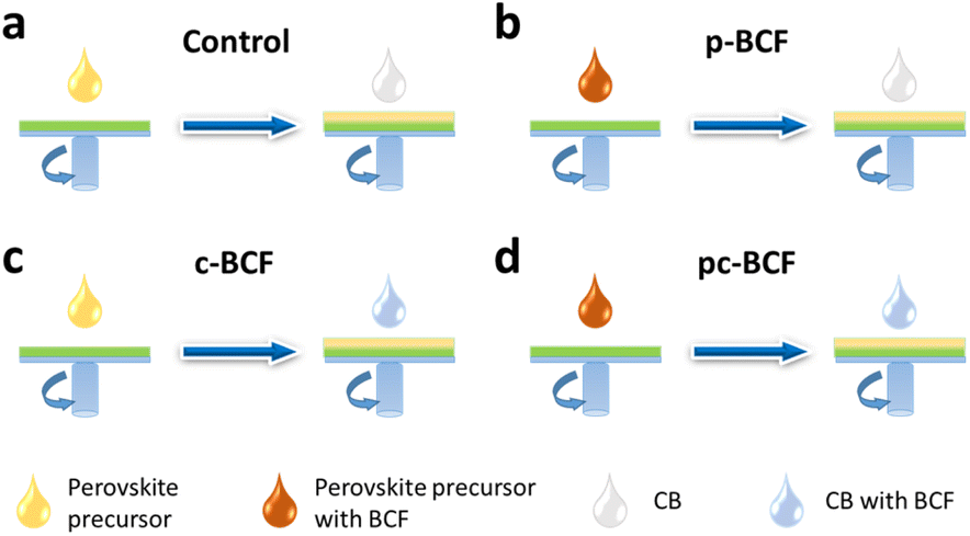 | ||
| Fig. 1 Schematic diagram of preparing perovskite films based on (a) control, (b) p-BCF, (c) c-BCF and (d) pc-BCF treatments. The first step is to spin coat the perovskite precursor, and the second step is to drip anti-solvent (CB). | ||
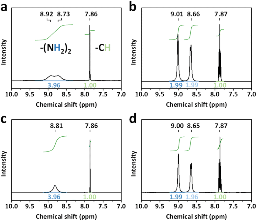 | ||
| Fig. 2 Liquid-state 1H NMR spectra (600 MHz, in pure DMSO-d6) of (a) FAI solution, (b) FAI solution with BCF, (c) perovskite solution and (d) perovskite solution with BCF. | ||
From the 1H-NMR full spectrum in Fig. S2a,† the peaks at 2.5 ppm and 3.3 ppm can be assigned to the methyl hydrogen on the DMSO and the hydroxyl hydrogen on the H2O, respectively.43 Although the solutions were prepared in a nitrogen box (PH2O < 0.1 ppm) and the NMR tubes for testing were just dried before use, and moisture absorption was still unavoidable. Interestingly, both spectra of FAI and perovskite solutions without BCF show a significant peak corresponding to H2O, while this peak is completely absent in the spectra of the solutions with BCF. The concentration of FAI is 0.1 M in all solutions, so the amount of water absorbed can be estimated. According to Fig. S2a,† the peak area belonging to H2O is nearly half as large as the peak area at 7.9 ppm, which represents the methyl hydrogen on the FA. It means that the moisture concentration absorbed by solution is about 0.025 M. As shown in Fig. S3,† there is still almost no characteristic peak of H2O in the magnified 1H NMR spectra of solutions with BCF (even the quadruple peak belonging to the ethanol impurity is found at about 3.4 ppm). The BCF molecule contains 15 F atoms, which make it highly hydrophobic.41 When BCF dissolves in solution, it can prevent moisture attack at the interface between the solution and atmosphere. Taking into account all these observations, the strong hydrogen bonding interaction between BCF and FA is thus demonstrated. This interaction could passivate the shallow-level defects caused by the FA vacancies in perovskite crystals, suppressing the migration of organic cations and enhancing the stability of the whole device. Additionally, benefited by the hydrophobicity of BCF, the hygroscopicity of perovskite solution is effectively inhibited, and even a tiny amount of water is difficult to intrude into the perovskite solution with BCF.
In order to investigate the surface chemical states and demonstrate the existence of BCF in the modified films, X-ray photoelectron spectroscopy (XPS) measurement is performed, as shown in Fig. 3a–c and S5.† All samples modified with BCF show a significant F 1s peak at about 688.5 eV, which is however absent in the control sample. This indicates that the BCF additive does exist on the surface of the modified perovskite films. In Fig. 3b, the strong peak at about 186.7 eV belongs to I 4 s emission and no peak for B appears. The main reason for the absence of the B 1s peak is that the atomic sensitivity factor (ASF) of B is 0.13, much smaller than that of F (1.00).39 Furthermore, the molar amount of B in BCF is only 1/15th that of F. As shown in Fig. 3c, the I 3d peaks of the control sample are located at 619.2 and 630.7 eV. The peaks shift to higher binding energies after BCF treatments, suggesting a robust interaction between the introduced BCF and I− within the perovskite films.42 As a strong Lewis acid, BCF has the ability to accept electrons from the under-coordinated halides and PbI3−, which would therefore passivate the corresponding deep-level defects45 and decrease non-radiative recombination16 for perovskite devices. As BCF does not have any interaction with Pb, the Pb 4f spectra for all the types of perovskite films are similar (Fig. S5e†). The XPS results demonstrate the passivation effect of all three BCF treatments for perovskite films.
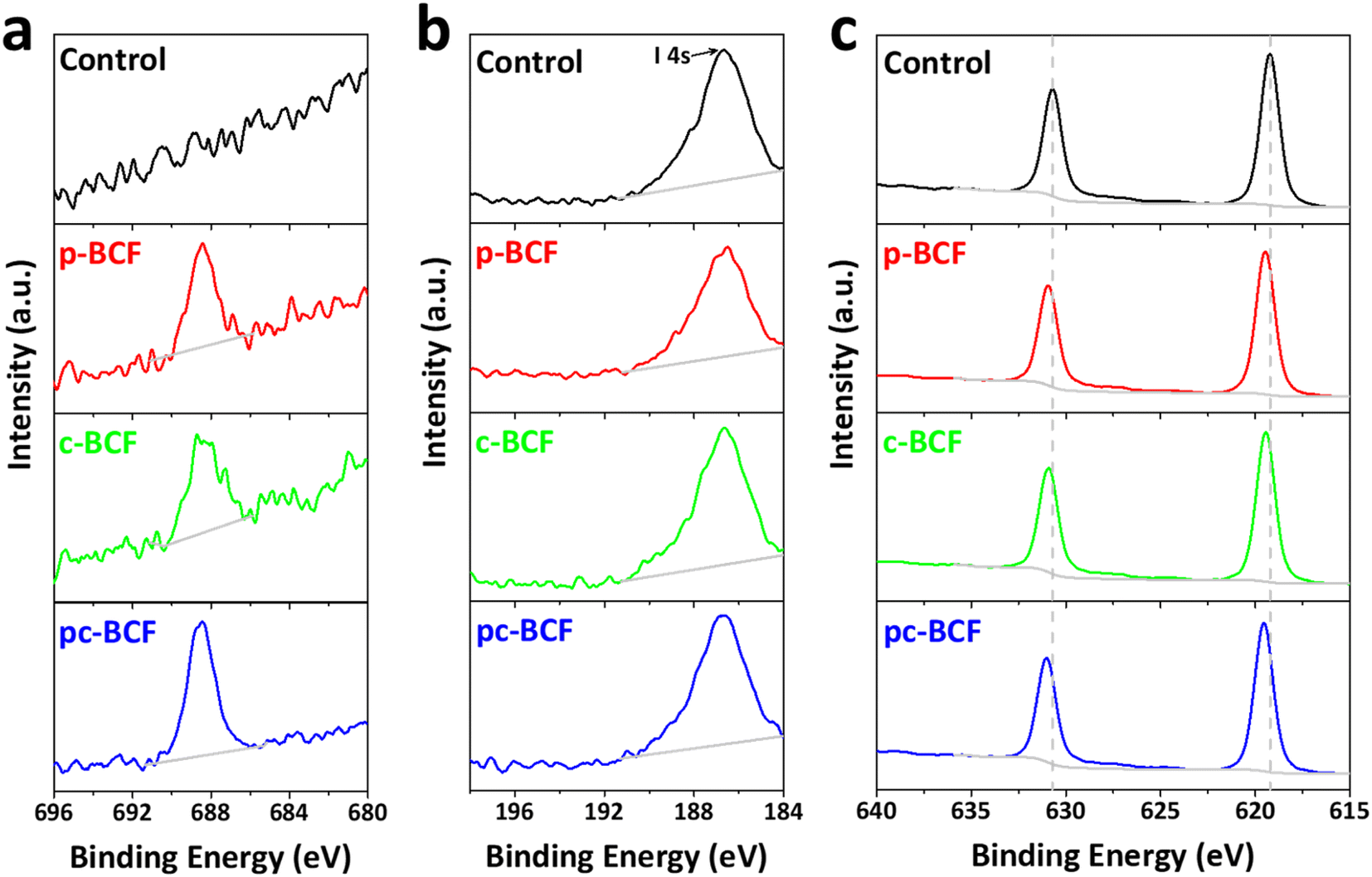 | ||
| Fig. 3 XPS spectra of (a) F 1s, (b) B 1s and (c) I 3d for the control, p-BCF, c-BCF and pc-BCF perovskite films. | ||
XPS is a surface sensitive analysis method, typically with a detection depth of less than 10 nm. Therefore, further measurements are needed to detect the distribution of BCF through the whole film depth. As BCF is soluble in various solvents, time-of-flight secondary ion mass spectrometry (TOF-SIMS) was conducted to determine whether the BCF in the perovskite film is tolerable to the washing processes of anti-solvent and solution coating of the HTM. By ejecting ions to etch the surface of the sample, an extremely small number of secondary ionic fragments are collected to determine their mass based on sputtering time. Fig. 4a and b show negative ion depth profiles corresponding to the multiple layers as a function of sputtering time for the films of spiro-OMeTAD/perovskite:BCF/SnO2/ITO. The CN− originates from organic materials which contain C–N bonds, so its trace covers both HTM and perovskite layers. The Br− and I− signals come from the perovskite layer, while the SnO− signal corresponds to the SnO2/ITO layer. By analyzing these ion traces, the component distribution through the depth of the whole film can be determined. In order to eliminate the interference of unnecessary fluorine sources, spiro-OMeTAD used here is pure without the additives of Li-TFSI and FK209 which contain fluorine element. So the variation of the F− signal can reflect the distribution of BCF in the depth of the films. The main difference between Fig. 4a and b is focused on the ion trace of F−. In Fig. 4a, the F− ion trace shows a weak peak at the interface between the perovskite and HTM layer (top interface) and a very strong peak at the interface between the perovskite and SnO2 layer (bottom interface). Meanwhile two peaks with similar strength are presented on the c-BCF sample in Fig. 4b. It is therefore concluded that the BCF can infiltrate into the perovskite layer via both DPMs and is enriched at the interfaces between perovskite and charge transporting layers. In the case of the p-BCF sample, the washing processes of anti-solvent and HTM coating decrease the concentration of BCF at the top interface and wash away extra BCF which does not interact with perovskite crystals. However, the washing effect cannot influence the bottom interface significantly and lead to a higher concentration of BCF accumulated at the interface. Such a high concentration of BCF could lead to the formation of a p-dopant functional layer, or even the formation of an insulation layer which may hinder electron transporting between the perovskite and electron transporting layer (ETL). For the c-BCF sample, the distribution of BCF above the bottom interface is similar to that of the p-BCF sample. Coating a c-BCF film is proceeded via anti-solvent and the concentration of BCF is enhanced at the interfaces. An appropriate amount of BCF infiltrates into the bottom interface and passivates the perovskite crystals without forming a blocking layer. The balanced distribution of the additive is very important to adjust to appropriate BCF concentration to optimize the device performance.
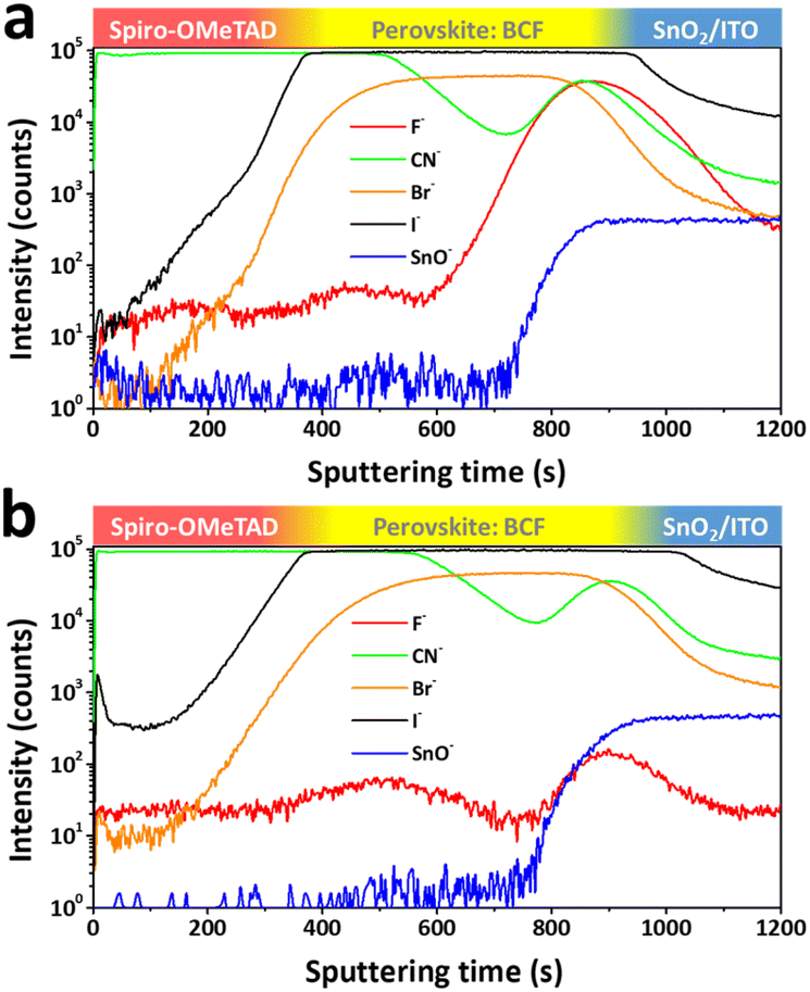 | ||
| Fig. 4 TOF-SIMIS of (a) p-BCF and (b) c-BCF samples based on the structure of spiro-OMeTAD/perovskite: BCF/SnO2/ITO. Negative ion depth profile mode is used. | ||
The morphologies of different perovskite films are characterized using top view scanning electron microscope (SEM) images (Fig. 5a–d). The control, p-BCF and c-BCF perovskite films display similar surface morphologies, which are dense, without any cracks or pinholes. An appropriate amount of BCF does not obstruct the development of perovskite crystals or the creation of the perovskite film. Meanwhile a relatively high concentration of BCF is generated on the top surface of the perovskite layer during the pc-BCF treatment when anti-solvent (containing BCF) is poured on. Due to the strong hydrogen bonding between BCF and FA, an excessive amount of BCF will make perovskite crystal formation too fast and excess solvent remains trapped in the film, which eventually leads to the emergence of voids when the excess solvent evaporates via annealing. The voids will be filled with the HTM and form a direct contact between the HTM and electron transporting material. Deleterious charge recombination will therefore be created, which deteriorates the photovoltaic performance of the device. Energy-dispersive X-ray spectroscopy (EDS) is applied to corroborate the presence and distribution of BCF in the perovskite films. Fig. S6–S8† show the SEM-EDS mapping of p-BCF, c-BCF and pc-BCF perovskite films, respectively. By comparing these images, it is confirmed that the BCF additive can distribute homogeneously on the surface of the perovskite layer. The cross-sectional SEM images of the PSCs based on different BCF treatments (Fig. S17†) indicate that all perovskite films have a similar thickness of approximately 750 nm (deviation ≤50 nm).
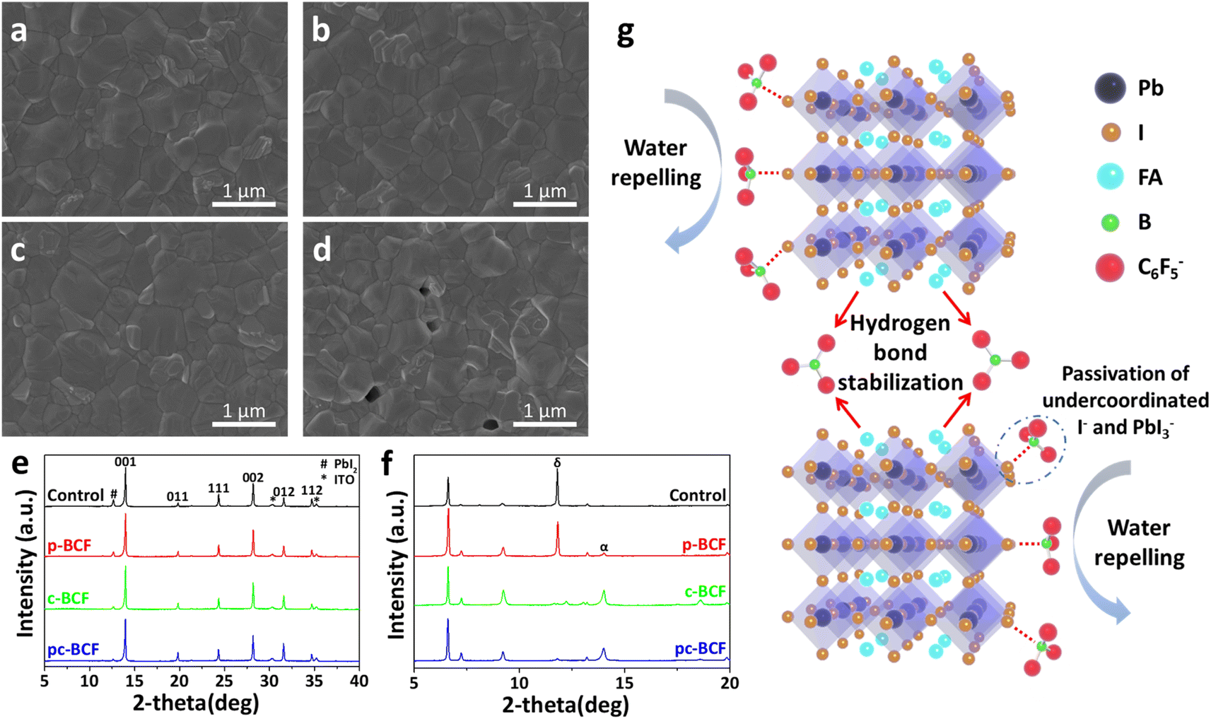 | ||
| Fig. 5 Top view SEM images of the (a) control, (b) p-BCF, (c) c-BCF and (d) pc-BCF perovskite films. XRD patterns of (e) annealed perovskite films and (f) unannealed perovskite films. (g) Schematic diagram of BCF modification at grain boundaries of perovskite. | ||
To further investigate the influence of BCF on the growth and quality of perovskite crystals, their X-ray diffraction (XRD) patterns are obtained. In Fig. 5e, all perovskite films display the crystal planes of (001), (011), (111), (002), (012) and (112), which are characteristic of the α phase perovskite.46 There is no discernible alteration in the peak distribution or emergence of new peaks, suggesting that BCF molecules will not enter into the crystal lattice or have impact on the crystal structure of the perovskite film. This observation aligns with the SEM images in Fig. 5a–d. Further, the peak at 12.6°, assigned to lead iodide (PbI2),45 is attenuated in the XRD intensity for all BCF samples compared to the control films. Under our experimental conditions, it should be pointed out that the addition of PbI2 is 5% excess to ensure the full conversion of perovskite from PbI2, so the existence of PbI2 in the XRD patterns is almost inevitable. However, the residual PbI2 is suppressed by BCF modification and almost disappears in the c-BCF and pc-BCF samples. These suggest that BCF can promote the transformation of PbI2 into perovskite and removal of residual PbI2 at the perovskite crystal boundaries. Except for the characteristic peaks of ITO at 30.3° and 35.2°,47 no other impurity peak can be found in all patterns of Fig. 5e. All perovskite films exhibit high crystal quality with no δ phase peak. To reveal the formation process of perovskite films, the XRD patterns of unannealed perovskite films are also obtained as depicted in Fig. 5f. The solvent is pure DMSO instead of a mixture of DMF and DMSO to simplify the solution system. In the unannealed films, there are three main forms of raw materials: FAI-PbI2-DMSO complex, α phase and δ phase perovskite. Three peaks at low angles (6.6°, 7.2° and 9.2°) are assigned to the intercalation of DMSO and FAI into PbI2, which forms a FAI-PbI2-DMSO intermediate complex.48 As there is no peak shifting at low angles compared to the control film, the introduction of BCF will not impede or exert a substantial impact on the formation of the FAI-PbI2-DMSO complex. The peaks at 11.8° and 14.0° are assigned to the δ phase and α phase perovskite, respectively.49 The δ phase perovskite with low photovoltaic properties should be eliminated in the perovskite films.27 The control and p-BCF samples exhibit a strong peak at 11.8° and a weak peak at 14.0°, implying the unwanted δ phase perovskite as the dominant component. In contrast, for the unannealed c-BCF and pc-BCF samples, the α phase dominates and the δ phase almost disappears. Since anti-solvent dripping is a washing process for the p-BCF sample, the BCF concentration decreases in this process (especially on the top surface). Meanwhile for c-BCF, it is a passivation process, during which the concentration of BCF increases. The different trends of BCF concentration in these two processes may be the key to inhibit the δ phase perovskite and promote the α phase. In summary, BCF can suppress the residue of PbI2 in the perovskite films, and the addition of BCF in anti-solvent can effectively accelerate the transformation of the α phase perovskite from δ phase perovskite.
Through the above measurements and analysis of perovskite films via different BCF treatments, we propose three pathways by which BCF may influence the photovoltaic performance of the perovskite devices, as illustrated in Fig. 5g. Firstly, BCF can form hydrogen bonds with FA to immobilize organic cations and inhibit ion migration. Meanwhile, BCF at grain boundaries could stabilize perovskite crystals through hydrogen bonding. Secondly, BCF can effectively passivate the under-coordinated I− and the PbI3− defects of perovskite, which could be instrumental in reducing non-radiative recombination of carriers. Thirdly, due to the presence of a large number of hydrophobic F groups in BCF, covering the surface of perovskite films with BCF may effectively improve the humidity stability of the devices. However, it is found from our results that not all DPMs utilizing the BCF additive can achieve the desired passivation effect. The selection of DPMs is crucial for the photovoltaic performance of perovskite films.
The perovskite solar cells are fabricated with a conventional planar structure ITO/SnO2/perovskite/spiro-OMeTAD/Au (Fig. 6a). In order to achieve the best passivation effect, control experiments are conducted on the effect of BCF concentration in two of the DPMs, p-BCF and c-BCF (Fig. S9 and Tables S1–S2†). For p-BCF treatment, the best photovoltaic performance is achieved when the concentration of BCF in the perovskite precursor is 10 mg mL—1, while the highest PCE is obtained via dissolving 3 mg mL−1 BCF in the anti-solvent for c-BCF treatment. The combination of the optimal concentrations of BCF in the perovskite precursor in the p-BCF cases with those in anti-solvent in the c-BCF cases is adopted in the pc-BCF preparation. The J–V curves based on the best control, p-BCF, c-BCF and pc-BCF PSCs are recorded in Fig. 6b with detailed device parameters in Table S3.† Among the four types of devices that utilize various treatments, the c-BCF device displays the most favorable photovoltaic performance with a PCE of 22.86%, short-circuit current density (Jsc) of 24.78 mA cm−2, open-circuit voltage (Voc) of 1.15 V, and fill factor (FF) of 80.09%. The performance of the p-BCF device with a PCE of 22.34% is a bit lower than that of the c-BCF device. The pc-BCF device yields the worst PCE of 18.91% which is even lower than that of the control device (19.88%). The J–V curves under different scan directions are provided in Fig. S10a and b.† In order to quantify the hysteresis effect, the hysteresis index (HI) is defined as:50
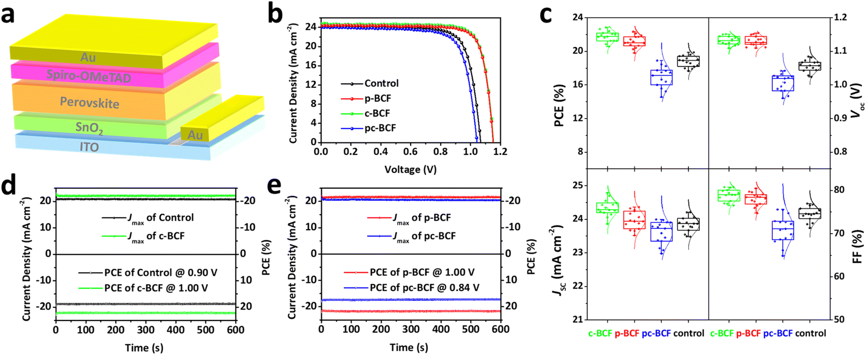 | ||
| Fig. 6 (a) Schematic illustration of the PSCs with a structure of ITO/SnO2/perovskite/spiro-OMeTAD/Au. (b) J–V curves of the best control, p-BCF, c-BCF and pc-BCF PSCs. (c) Statistical distribution of photovoltaic parameters for each of the 15 PSCs fabricated from different DPMs. Stabilized power output (SPO) measured for 600 s at the maximum power point (MPP) of (d) the control and c-BCF PSCs, (e) p-BCF and pc-BCF PSCs. | ||
The HI values of 0.055, 0.028, 0.032 and 0.063 are presented for PSCs based on control, c-BCF, p-BCF and pc-BCF treatments, showing the negligible hysteresis of properly modified devices. The reduction in the HI may be attributed to the suppressed ion migration and reduced defects by passivation.51 The corresponding incident photon-to-electron conversion efficiency (IPCE) spectra and calculated integrated Jsc are also given in Fig. S10c and d.† The c-BCF device presents the highest integrated Jsc and the calculated Jsc values of the four devices are similar to the Jsc obtained from J–V curves.52
As depicted in TOF-SIMS and XRD measurements, the c-BCF treatment can modify the perovskite film homogeneously, suppressing the formation of the δ phase while facilitating the formation of the α phase perovskite. Meanwhile p-BCF treatment may form a blocking layer between the perovskite and SnO2 layers, leading to impeded charge carrier transport. By comparing the statistical distribution of photovoltaic parameters (Fig. 6c), it can be found that the average Jsc of the c-BCF devices is higher than that of the other devices. The increase in the current density of the c-BCF devices is mainly due to the fact that BCF promotes the growth of α phase perovskite and improves the crystallinity of the perovskite film. Meanwhile, this improvement is not obvious for the p-BCF devices. Importantly, the unwanted BCF blocking layer in the p-BCF devices could impede charge extraction and thus increase the series resistance inside the device. The superior Voc and FF of both c-BCF and p-BCF devices can be attributed to the excellent passivation from BCF, which reduces the defect density of perovskite layers. However, performance deterioration occurs in the pc-BCF devices. During the fabrication of pc-BCF devices, upon the BCF-containing anti-solvent is added dropwise onto the perovskite film, a large number of cracks are generated in the film (Fig. S11†), seriously affecting the photovoltaic performance of the device. Interestingly, similar cracks also appear during the preparation of p-BCF and c-BCF devices with relatively high BCF concentration. During the pc-BCF treatment, the film is treated with BCF twice, resulting in a high concentration of BCF in the film. These observations indicate that an excessive concentration of BCF can lead to the formation of cracks and the deterioration of perovskite films. From the aforementioned SEM images (Fig. 5d), it is also found that the perovskite film by pc-BCF treatment exhibits more voids and poor film quality, which seriously lower device performance. Therefore, the dosage of BCF is crucial for the defect passivation and quality of perovskite films. The stabilized power output (SPO) measured at the maximum power point (MPP) is shown in Fig. 6d and e. The continuous SPOs are relatively stable by holding the samples at the maximum power point for 600 s. The c-BCF PSC still shows the best SPO PCE of about 22.17%, while the control device shows about 18.64%.
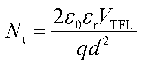
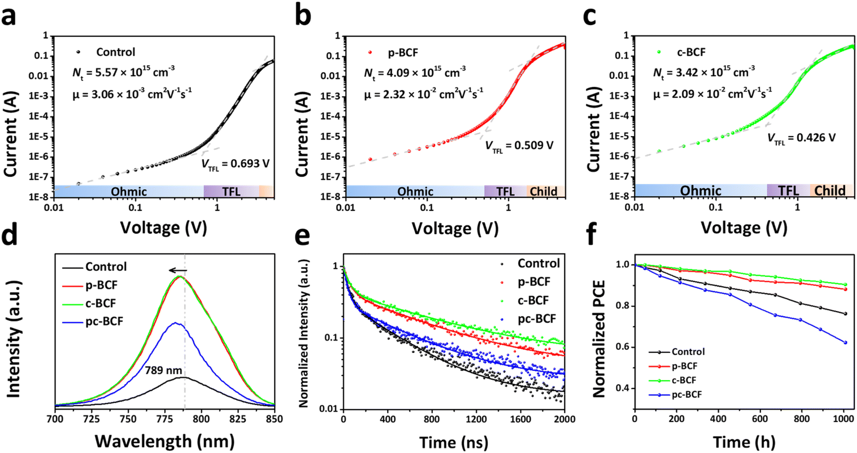
To further understand the carrier transport process in the devices, space-charge limited current (SCLC) measurements are performed. The dark current–voltage (I–V) curves of hole-only devices with the configuration of glass/ITO/Au/perovskite/Au are exhibited in Fig. 7a–c. Typical three regions with an exponential relationship of I ∝ Vn are evident in the experimental data (except for pc-BCF devices which will be discussed in Fig. S12†). At low voltages, the I–V curve presents a linear ohmic regime (I ∝ V). In the intermediate regime, the trap states become occupied by the injected carriers with the rapid current increase (I ∝ Vn, n > 3) and the trap-filled limit (TFL) regime is reached. The voltage required for the trapped space-charge is defined as the onset voltage (VTFL), which could be obtained by fitting the curves of the first two regions. The trap density (Nt) can be calculated as follows:53
where μ is the carrier mobility and Va is the applied voltage. According to the Mott–Gurney law, carrier mobility can be obtained from the slope of the
 curves in the high region. The hole mobilities of both c-BCF (2.09 × 10⁻² cm2 V−1 s−1) and p-BCF (2.32 × 10⁻² cm2 V−1 s−1) films are about one order of magnitude larger than that of the control (3.06 × 10⁻³ cm2 V−1 s−1) film, which should be ascribed to the low trap density and high quality of the films. The SCLC measurements have demonstrated the effective suppression of defect density and the improvement of carrier transport in perovskite films by suitable BCF modification. Meanwhile unsuitable BCF modification (pc-BCF) forms a poor quality perovskite film with many pinholes, which will lead to direct contact between gold electrodes on both sides and thus causes a large leakage current to exceed the measurement range (Fig. S12†).
 | ||
| Fig. 7 Dark current–voltage (I–V) curves with the configuration of hole-only devices for (a) control, (b) p-BCF and (c) c-BCF perovskite films. (d) PL spectra and (e) normalized TRPL decay curves of the control, p-BCF, c-BCF and pc-BCF perovskite films. (f) Long term stability tests of different PSCs for more than 1000 h under ambient conditions (10–25 °C and 45 ± 10% RH). | ||
The absorption spectra of perovskite films are recorded through the use of ultraviolet-visible (UV-vis) spectroscopy, as depicted in Fig. S13.† All types of BCF treated perovskite films show a slightly enhanced absorption. The steady photoluminescence (PL) spectra of perovskite films prepared under different conditions are shown in Fig. 7d. The PL intensities of the c-BCF and p-BCF perovskite films are much stronger than those of the control one, implying that the non-radiative recombination from defects has been remarkably suppressed.56 Enhanced PL intensity by the pc-BCF treatment is also observed, but not as strong as those on the c-BCF or p-BCF samples, indicating a less effective passivation. The control film shows a peak in PL emission at 789 nm and a blue shift of the peak is observed in all BCF-modified perovskite films. When the shallow traps near the band edge are removed, excitons will not be easily captured by these traps but recombine radiatively by releasing a photon with a higher energy, leading to the blue shift of the emission peak.57 The blue shift of the PL emission observed here is attributed to the reduced shallow trap density on the surface and at grain boundaries as a result of the passivation effect of BCF. This is in line with the time-resolved photoluminescence spectra (TRPL) results in Fig. 7e (the fitted parameters are listed in Table S4†). The average lifetime τave of the c-BCF (694.62 ns) and p-BCF (587.88 ns) films is relatively longer than those of the pc-BCF (406.12 ns) and control samples (309.08 ns). These results validate that an appropriate pathway for the BCF treatment can increase the recombination lifetime and reduce the non-radiative recombination of perovskite films. As the non-radiative recombination is responsible for the Voc loss,58 the Voc enhancement of c-BCF and p-BCF PSCs should originate from the suppressed trap defects by BCF passivation. For p-type dopant BCF, the c-BCF treatment is the best pathway to passivate perovskite films in PSCs. The p-BCF treatment can cause a high concentration of BCF at the bottom interface of PSCs, hindering carrier transport and resulting in a reduction in short-circuit current. If an n-type dopant to promote electron transport at the perovskite/ETL interface is employed as the additive, the DPMs like p-BCF may be a better choice. Meanwhile, for additives with high concentrations that can easily affect the crystallinity and film morphology of perovskite, the treatments like pc-BCF need to be used with caution.
The long term stability of different PSCs under ambient conditions (10–25 °C and 45 ± 10% RH) is evaluated in Fig. 7f. The c-BCF device maintains more than 90% of its initial PCE for 1000 h, which is much better than that of the control device (76%). The PCE degradation trend of the p-BCF device (88% PCE for 1000 h) is similar to that of the c-BCF device. Meanwhile the PCE of pc-BCF decreases to 62% of the initial value implying a rapid degradation. The improved stability of the c-BCF and p-BCF devices should be attributed to the successful passivation achieved through the BCF treatment, along with the hydrophobicity of BCF. The rapid degradation of the pc-BCF device may be attributed to the low quality of the perovskite film, which contains numerous cracks and voids. The moisture resistance of the BCF treated perovskite films is confirmed by water contact angle measurements in Fig. S14.† Both c-BCF and p-BCF films present a higher water contact angle than the control film. The poor morphology of the pc-BCF film, characteristic of a large number of cracks and voids, would increase the roughness of the perovskite film and accelerate the infiltration of water into the perovskite film. The contact angle decreases with increasing roughness, when it is smaller than a certain transition angle.59 The surface hydrophobicity of the pc-BCF film may be compromised, resulting in a relatively lower water contact angle of the pc-BCF film. To further verify the moisture resistance, perovskite films based on different BCF treatments were aged under high humidity conditions (75 ± 5% RH) for 18 days (Fig. S15†). The c-BCF and p-BCF films are still stable, while significant degradation occurs in control and pc-BCF films after aging. The XRD spectra of the perovskite films before and after aging (Fig. S16†) also provide the same conclusion.
Conclusions
In summary, the influence of various BCF based DPMs on perovskite films and PSCs is well investigated. p-BCF treatment can lead to the enrichment of additives on the bottom surface of perovskite films, while the c-BCF treatment makes the additives dispersed homogeneously in the film. This situation is different from additives that can only be dissolved in the perovskite precursor or anti-solvent. Therefore, it is necessary to select the optimal DPM based on the solubility of additives in diversified solvents. BCF can form hydrogen bonds with C–H and N–H in perovskite, immobilizing FA and inhibiting the migration of organic cations. The ability of a Lewis acid to acquire electrons enables it to passivate the under-coordinated I− and PbI3− defects, suppressing non-radiative recombination. In addition, selecting an appropriate DPM can also eliminate the generation of δ phase perovskite and make the distribution of BCF more reasonable. Among three types of DPMs, c-BCF results in the best photovoltaic performance of PSCs, achieving the highest PCE of 22.86% with negligible hysteresis. The performance of the p-BCF treated device is slightly lower than that of c-BCF. The devices based on the above two treatments have shown excellent stability. This work provides a novel perspective for the selection of DPMs to achieve high performance and stable PSCs.Experimental section
Chemicals and materials
Unless stated otherwise, all chemicals were used as received without further purification. Lead(II) iodide (PbI2), lead(II) bromide (PbBr2) and cesium iodide (CsI) were purchased from TCI. N,N-Dimethylformamide (DMF), dimethyl sulfoxide (DMSO), chlorobenzene (CB) and tris(pentafluorophenyl)borane (BCF) were purchased from Sigma-Aldrich. Formamidinium iodide (FAI), methylammonium bromine (MABr), methylamine chloride (MACl) and 2,2′,7,7′-tetrakis(N,N-di-p-methoxyphenylamine)-9,9-spirobifluorene (spiro-OMeTAD) were purchased from Xi'an Polymer Light Technology Corporation. The tin oxide (SnO2) colloidal dispersion, 4-tert-butylpyridine (tBP), lithium bis(trifluoromethylsulphonyl)imide (Li-TFSI) and tris(2-(1H-pyrazol-1-yl)-4-tert-butylpyridine)cobalt(III) bis(trifluoro-methylsulphonyl)imide (FK209) were acquired from Alfa Aesar.Solution preparation
Two kinds of SnO2 solutions were obtained by diluting SnO2 colloid dispersion in water at a volume ratio of 1![[thin space (1/6-em)]](https://www.rsc.org/images/entities/char_2009.gif) :6 by dissolving 7 mg and 14 mg NH4Cl, respectively. The perovskite (Cs0.03FA0.97PbI3)0.95(MAPbBr3)0.05 precursor solution with 22 mg mL−1 MACl was prepared in a stoichiometric ratio of FAI, MABr, CsI, PbI2 and PbBr2 to make the concentration of Pb2+ to be 1.6 M in DMF/DMSO mixed solvents (volume ratio of 8:2) in a glovebox. The solution was stirred until fully dissolved for more than 1 h and filtered before use. Various doses of BCF were added into the perovskite precursors or anti-solvents for the required defect passivation methods. Spiro-OMeTAD solution was prepared by mixing 73.5 mg spiro-OMeTAD, 29 μL tBP, 17 μL Li-TFSI (500 mg in 1 mL of acetonitrile), and 8 μL FK209 (400 mg in 1 mL of acetonitrile) in 1 mL chlorobenzene.
:6 by dissolving 7 mg and 14 mg NH4Cl, respectively. The perovskite (Cs0.03FA0.97PbI3)0.95(MAPbBr3)0.05 precursor solution with 22 mg mL−1 MACl was prepared in a stoichiometric ratio of FAI, MABr, CsI, PbI2 and PbBr2 to make the concentration of Pb2+ to be 1.6 M in DMF/DMSO mixed solvents (volume ratio of 8:2) in a glovebox. The solution was stirred until fully dissolved for more than 1 h and filtered before use. Various doses of BCF were added into the perovskite precursors or anti-solvents for the required defect passivation methods. Spiro-OMeTAD solution was prepared by mixing 73.5 mg spiro-OMeTAD, 29 μL tBP, 17 μL Li-TFSI (500 mg in 1 mL of acetonitrile), and 8 μL FK209 (400 mg in 1 mL of acetonitrile) in 1 mL chlorobenzene.
Device fabrication
ITO glass (1.5 × 2 cm2) was cleaned in an ultrasonic bath containing deionized water and ethanol for 30 min each time, dried with flowing nitrogen gas, and then treated with ultraviolet ozone for 30 min. SnO2 solution (100 μL) containing 7 mg mL−1 NH4Cl was spin-coated on the substrate at 4000 rpm for 50 s, and an equal volume of SnO2 solution containing 14 mg mL−1 NH4Cl was added dropwise at the 25th second. Subsequently, the film was annealed at 90 °C for 1 hour. The perovskite precursor (35 μL, with or without BCF) was spin-coated in a dry air flowing glovebox by a consecutive two-step spin-coating process at 1000 rpm and 4600 rpm for 10 s and 30 s, respectively. In the last 15 s of the second spin-coating step, the substrate was treated with 150 μL of chlorobenzene (with or without BCF) as the anti-solvent. Afterwards, the film was annealed at 150 °C for 15 min. 40 μL of spiro-OMeTAD solution was spin-coated onto the perovskite layer at 3000 rpm for 20 s. Finally, an 80 nm gold electrode was thermally evaporated on top of the device.Characterization
Unless stated otherwise, the solutions containing BCF applied in all measurements were at the concentration for optimal PSC fabrication (10 mg mL−1 in the perovskite precursor for p-BCF, 3 mg mL−1 in CB for c-BCF, 10 mg mL−1 in the perovskite precursor and 3 mg mL−1 in CB for pc-BCF). The 1H NMR spectra were recorded on a 600 MHz liquid NMR spectrometer (Bruker, AVANCE III 600 MHz 54 mm−1) and DMSO-d6 was used as solvent to dissolve 0.1 M FAI and 0.1 M FAPbI3 (with or without 25 mg mL−1 BCF). FTIR spectra were recorded with a Thermo Scientific iS50R FT-IR spectrometer. Perovskite precursor solution containing 20 mg mL−1 BCF was applied in Per.+BCF samples for both liquid and powder measurements. XPS characterization was performed with a Thermo ESCALAB 250Xi X-ray Photoelectron Spectrometer by using a monochromatized Al Kα source (hν = 1486.6 eV, 150 W) with a 500 μm sized X-ray beam spot (hydrocarbon C 1s located at 284.8 eV is used for energy referencing). The TOF-SIMS measurement of perovskite films was conducted with a TOF-SIMS 5 IONTOF via negative ion depth profile mode (primary ion Bi1, energy 30 keV, and current 1.00 pA; sputter ion Cs, energy 1 keV, and current 60.00 nA). The morphologies of all samples were characterized with a cold field-emission scanning electron microscope (SU8220, Hitachi), equipped with an X-ray spectrometer (Aztec Oxford) for EDS mapping. XRD patterns were obtained with a Micro-diffractometer (Rigaku SmartLab 9kW, Nippon Institute of Science and Technology Co., Ltd, Japan) using Cu Kα radiation (λ = 1.5406 Å). UV-vis absorption spectra were acquired on a UV-vis spectrophotometer (SOLID3700, Shimadzu, Japan) acquired in absorption mode. The PL and TRPL spectra (excited at 450 nm) were recorded on a JY Fluorolog-3-Tou fluorescence spectrophotometer (Jobin Yvon, France). Contact angles were determined on an OCA15EC contact angle measuring instrument (Dataphysics, Germany) with a drop of ultrapure water.The J–V curves were recorded on a solar simulator (Enlitech, SS-F5-3A) with a source meter (Keysight B2901A SMU). The solar simulator with 100 mW cm−2 illumination (AM 1.5 G) was calibrated by using a NREL certified silicon reference cell (SRC-2020). The device area of 0.09 cm2 was defined by masking a metal mask to avoid light scattering from the metal electrode onto the device during the measurement. The IPCE was measured using an IPCE measuring system (Newport Corporation, CA) equipped with a Xe lamp as the light source.
Data availability
The data supporting this study are available within the main text and the ESI.†Author contributions
L. Z.: formal analysis, funding acquisition, investigation, methodology, validation, visualization, and writing – original draft. S. X.: investigation and validation. G. L.: investigation and validation. L. L.: methodology. H. Z.: formal analysis. Z. A.: formal analysis. X. P.: conceptualization, funding acquisition, project administration, resources, and supervision. F. Z.: conceptualization, data curation, funding acquisition, resources, supervision, and writing – review & editing.Conflicts of interest
There are no conflicts to declare.Acknowledgements
This work was financially supported by the National Natural Science Foundation of China (Grant no. 11904366 and U22A20142), the National Key Research and Development Program of China (Grant no. 2021YFA1600202), the Anhui Provincial Natural Science Foundation (Grant no. 1908085ME152) and the Science Funds of Distinguished Young Scholars of Anhui Province (Grant no. 5542108085J34). The authors appreciate Prof. Yunyan Li at the High Magnetic Field Laboratory for assistance in the operation of the nuclear magnetic resonance instrument.Notes and references
- A. Kojima, K. Teshima, Y. Shirai and T. Miyasaka, J. Am. Chem. Soc., 2009, 131, 6050–6051 CrossRef CAS PubMed.
- G. Xing, N. Mathews, S. S. Lim, N. Yantara, X. Liu, D. Sabba, M. Gratzel, S. Mhaisalkar and T. C. Sum, Nat. Mater., 2014, 13, 476–480 CrossRef CAS PubMed.
- Z. K. Tan, R. S. Moghaddam, M. L. Lai, P. Docampo, R. Higler, F. Deschler, M. Price, A. Sadhanala, L. M. Pazos, D. Credgington, F. Hanusch, T. Bein, H. J. Snaith and R. H. Friend, Nat. Nanotechnol., 2014, 9, 687–692 CrossRef CAS PubMed.
- T. Y. Yang, G. Gregori, N. Pellet, M. Gratzel and J. Maier, Angew. Chem., Int. Ed., 2015, 54, 7905–7910 CrossRef CAS PubMed.
- L. Dou, Y. M. Yang, J. You, Z. Hong, W. H. Chang, G. Li and Y. Yang, Nat. Commun., 2014, 5, 5404 CrossRef CAS PubMed.
- T. Wu, Z. Qin, Y. Wang, Y. Wu, W. Chen, S. Zhang, M. Cai, S. Dai, J. Zhang, J. Liu, Z. Zhou, X. Liu, H. Segawa, H. Tan, Q. Tang, J. Fang, Y. Li, L. Ding, Z. Ning, Y. Qi, Y. Zhang and L. Han, Nano-Micro Lett., 2021, 13, 152 CrossRef CAS PubMed.
- Y. Zhao, F. Ma, Z. Qu, S. Yu, T. Shen, H. X. Deng, X. Chu, X. Peng, Y. Yuan, X. Zhang and J. You, Science, 2022, 377, 531–534 CrossRef CAS PubMed.
- H. Zhang, J. W. Lee, G. Nasti, R. Handy, A. Abate, M. Gratzel and N. G. Park, Nature, 2023, 617, 687–695 CrossRef CAS PubMed.
- R. Azmi, E. Ugur, A. Seitkhan, F. Aljamaan, A. S. Subbiah, J. Liu, G. T. Harrison, M. I. Nugraha, M. K. Eswaran, M. Babics, Y. Chen, F. Xu, T. G. Allen, A. U. Rehman, C. L. Wang, T. D. Anthopoulos, U. Schwingenschlogl, M. De Bastiani, E. Aydin and S. De Wolf, Science, 2022, 376, 73–77 CrossRef CAS PubMed.
- R. Lin, J. Xu, M. Wei, Y. Wang, Z. Qin, Z. Liu, J. Wu, K. Xiao, B. Chen, S. M. Park, G. Chen, H. R. Atapattu, K. R. Graham, J. Xu, J. Zhu, L. Li, C. Zhang, E. H. Sargent and H. Tan, Nature, 2022, 603, 73–78 CrossRef CAS PubMed.
- NREL, Best Research-Cell Efficiency Chart, https://www.nrel.gov/pv/cell-efficiency.html, accessed October 2023 Search PubMed.
- A. Polman, M. Knight, E. C. Garnett, B. Ehrler and W. C. Sinke, Science, 2016, 352, aad4424 CrossRef PubMed.
- A. R. b. Mohd Yusoff, M. Vasilopoulou, D. G. Georgiadou, L. C. Palilis, A. Abate and M. K. Nazeeruddin, Energy Environ. Sci., 2021, 14, 2906–2953 RSC.
- T. H. Han, S. Tan, J. Xue, L. Meng, J. W. Lee and Y. Yang, Adv. Mater., 2019, 31, e1803515 CrossRef PubMed.
- L. K. Ono, S. F. Liu and Y. Qi, Angew. Chem., Int. Ed., 2020, 59, 6676–6698 CrossRef CAS PubMed.
- F. Zhang and K. Zhu, Adv. Energy Mater., 2020, 10, 1902579 CrossRef CAS.
- K. R. Yan, Z. Q. Shen, B. F. Niu, Y. C. Huang, D. Wang, E. Gu, B. Y. Yan, J. Z. Yao, H. Z. Chen and C. Z. Li, Sci. China: Chem., 2023, 66, 1795–1803 CrossRef CAS.
- T. Y. Wen, S. Yang, P. F. Liu, L. J. Tang, H. W. Qiao, X. Chen, X. H. Yang, Y. Hou and H. G. Yang, Adv. Energy Mater., 2018, 8, 1703143 CrossRef.
- J. Huang, H. Wang, C. Chen, Y. Tang, H. Yang, S. Liu and D. Zhang, Chem. Eng. J., 2023, 466, 143120 CrossRef CAS.
- X. Zheng, Y. Deng, B. Chen, H. Wei, X. Xiao, Y. Fang, Y. Lin, Z. Yu, Y. Liu, Q. Wang and J. Huang, Adv. Mater., 2018, 30, e1803428 CrossRef PubMed.
- G. Z. Liu, H. Y. Zheng, J. J. Ye, S. D. Xu, L. Y. Zhang, H. F. Xu, Z. Liang, X. J. Chen and X. Pan, ACS Energy Lett., 2021, 6, 4395–4404 CrossRef CAS.
- J. Park, J. Kim, H. S. Yun, M. J. Paik, E. Noh, H. J. Mun, M. G. Kim, T. J. Shin and S. I. Seok, Nature, 2023, 616, 724–730 CrossRef CAS PubMed.
- H. Y. Zheng, L. Z. Zhu, L. H. Hu, S. F. Yang, S. H. Chen, A. Alsaedi, T. Hayat, Y. Huang, X. Pan and S. Y. Dai, J. Mater. Chem. A, 2018, 6, 9930–9937 RSC.
- J. W. Lee, Z. Dai, T. H. Han, C. Choi, S. Y. Chang, S. J. Lee, N. De Marco, H. Zhao, P. Sun, Y. Huang and Y. Yang, Nat. Commun., 2018, 9, 3021 CrossRef PubMed.
- H. Y. Zheng, G. Z. Liu, L. Z. Zhu, J. J. Ye, X. H. Zhang, A. Alsaedi, T. Hayat, X. Pan and S. Y. Dai, Adv. Energy Mater., 2018, 8, 1800051 CrossRef.
- J. Jeong, M. Kim, J. Seo, H. Lu, P. Ahlawat, A. Mishra, Y. Yang, M. A. Hope, F. T. Eickemeyer, M. Kim, Y. J. Yoon, I. W. Choi, B. P. Darwich, S. J. Choi, Y. Jo, J. H. Lee, B. Walker, S. M. Zakeeruddin, L. Emsley, U. Rothlisberger, A. Hagfeldt, D. S. Kim, M. Gratzel and J. Y. Kim, Nature, 2021, 592, 381–385 CrossRef CAS PubMed.
- W. Hui, L. Chao, H. Lu, F. Xia, Q. Wei, Z. Su, T. Niu, L. Tao, B. Du, D. Li, Y. Wang, H. Dong, S. Zuo, B. Li, W. Shi, X. Ran, P. Li, H. Zhang, Z. Wu, C. Ran, L. Song, G. Xing, X. Gao, J. Zhang, Y. Xia, Y. Chen and W. Huang, Science, 2021, 371, 1359–1364 CrossRef CAS PubMed.
- Y. Wang, M. D. X. Han, R. B. Wang, J. T. Zhao, J. W. Zhang, H. Z. Ren, G. F. Hou, Y. Ding, Y. Zhao and X. D. Zhang, J. Mater. Chem. A, 2023, 11, 8573–8598 RSC.
- Q. Jiang, Y. Zhao, X. Zhang, X. Yang, Y. Chen, Z. Chu, Q. Ye, X. Li, Z. Yin and J. You, Nat. Photonics, 2019, 13, 460–466 CrossRef CAS.
- M. H. Li, H. H. Yeh, Y. H. Chiang, U. S. Jeng, C. J. Su, H. W. Shiu, Y. J. Hsu, N. Kosugi, T. Ohigashi, Y. A. Chen, P. S. Shen, P. Chen and T. F. Guo, Adv. Mater., 2018, 30, e1801401 CrossRef PubMed.
- N. Ghimire, R. S. Bobba, A. Gurung, K. M. Reza, M. A. R. Laskar, B. S. Lamsal, K. Emshadi, R. Pathak, M. A. Afroz, A. H. Chowdhury, K. Chen, B. Bahrami, S. I. Rahman, J. Pokharel, A. Baniya, M. T. Rahman, Y. Zhou and Q. Qiao, ACS Appl. Energy Mater., 2021, 4, 1731–1742 CrossRef CAS.
- S. Han, S.-K. Hyeong, S.-K. Lee and N. Shin, Chem. Eng. J., 2022, 439, 135715 CrossRef CAS.
- N. Wei, Y. T. Chen, X. T. Wang, Y. F. Miao, Z. X. Qin, X. M. Liu, H. Wei and Y. X. Zhao, Adv. Funct. Mater., 2022, 32, 2108944 CrossRef CAS.
- H. Zhao, Z. Xu, Y. Che, Y. Han, S. Yang, C. Duan, J. Cui, S. Dai, Z. Liu and S. Liu, J. Power Sources, 2021, 492, 229580 CrossRef CAS.
- P. F. Xie, H. Xiao, Y. Qiao, G. P. Qu, J. Z. Chen, X. Y. Liu and Z. X. Xu, Chem. Eng. J., 2023, 462, 142328 CrossRef CAS.
- S. Tan, T. Huang, I. Yavuz, R. Wang, T. W. Yoon, M. Xu, Q. Xing, K. Park, D. K. Lee, C. H. Chen, R. Zheng, T. Yoon, Y. Zhao, H. C. Wang, D. Meng, J. Xue, Y. J. Song, X. Pan, N. G. Park, J. W. Lee and Y. Yang, Nature, 2022, 605, 268–273 CrossRef CAS PubMed.
- J. S. Luo, J. X. Xia, H. Yang, L. L. Chen, Z. Q. Wan, F. Han, H. A. Malik, X. H. Zhu and C. Y. Jia, Energy Environ. Sci., 2018, 11, 2035–2045 RSC.
- J. Luo, J. Xia, H. Yang, H. A. Malik, F. Han, H. Shu, X. Yao, Z. Wan and C. Jia, Nano Energy, 2020, 70, 104509 CrossRef CAS.
- S. S. Reddy, V. M. Arivunithi, V. G. Sree, H. Kwon, J. Park, Y.-C. Kang, H. Zhu, Y.-Y. Noh and S.-H. Jin, Nano Energy, 2019, 58, 284–292 CrossRef CAS.
- T. Ye, J. Wang, W. Chen, Y. Yang and D. He, ACS Appl. Mater. Interfaces, 2017, 9, 17923–17931 CrossRef CAS PubMed.
- C. W. Koh, J. H. Heo, M. A. Uddin, Y. W. Kwon, D. H. Choi, S. H. Im and H. Y. Woo, ACS Appl. Mater. Interfaces, 2017, 9, 43846–43854 CrossRef CAS PubMed.
- S. Yuan, F. Qian, S. Yang, Y. Cai, Q. Wang, J. Sun, Z. Liu and S. Liu, Adv. Funct. Mater., 2019, 29, 1807850 CrossRef CAS.
- M. Yavari, M. Mazloum-Ardakani, S. Gholipour, N. Marinova, J. L. Delgado, S. H. Turren-Cruz, K. Domanski, N. Taghavinia, M. Saliba, M. Gratzel, A. Hagfeldt and W. Tress, Adv. Energy Mater., 2018, 8, 1702719 CrossRef.
- Y. Y. Hao, X. Z. Wang, M. Z. Zhu, X. F. Jiang, L. Wang, G. R. Cao, S. P. Pang and Z. M. Zhou, J. Mater. Chem. A, 2022, 10, 13048–13054 RSC.
- M. Du, X. Zhu, L. Wang, H. Wang, J. Feng, X. Jiang, Y. Cao, Y. Sun, L. Duan, Y. Jiao, K. Wang, X. Ren, Z. Yan, S. Pang and S. F. Liu, Adv. Mater., 2020, 32, e2004979 CrossRef PubMed.
- A. A. Zhumekenov, M. I. Saidaminov, M. A. Haque, E. Alarousu, S. P. Sarmah, B. Murali, I. Dursun, X. H. Miao, A. L. Abdelhady, T. Wu, O. F. Mohammed and O. M. Bakr, ACS Energy Lett., 2016, 1, 32–37 CrossRef CAS.
- H. Tan, A. Jain, O. Voznyy, X. Lan, F. P. Garcia de Arquer, J. Z. Fan, R. Quintero-Bermudez, M. Yuan, B. Zhang, Y. Zhao, F. Fan, P. Li, L. N. Quan, Y. Zhao, Z. H. Lu, Z. Yang, S. Hoogland and E. H. Sargent, Science, 2017, 355, 722–726 CrossRef CAS PubMed.
- N. J. Jeon, J. H. Noh, Y. C. Kim, W. S. Yang, S. Ryu and S. I. Seok, Nat. Mater., 2014, 13, 897–903 CrossRef CAS PubMed.
- H. Min, M. Kim, S. U. Lee, H. Kim, G. Kim, K. Choi, J. H. Lee and S. I. Seok, Science, 2019, 366, 749–753 CrossRef CAS PubMed.
- W. Z. Xu, T. Zhu, Y. R. Yang, L. Y. Zheng, L. Liu and X. Gong, Adv. Funct. Mater., 2020, 30, 2002808 CrossRef CAS.
- Y. Ding, B. Ding, H. Kanda, O. J. Usiobo, T. Gallet, Z. Yang, Y. Liu, H. Huang, J. Sheng, C. Liu, Y. Yang, V. I. E. Queloz, X. Zhang, J. N. Audinot, A. Redinger, W. Dang, E. Mosconic, W. Luo, F. De Angelis, M. Wang, P. Dorflinger, M. Armer, V. Schmid, R. Wang, K. G. Brooks, J. Wu, V. Dyakonov, G. Yang, S. Dai, P. J. Dyson and M. K. Nazeeruddin, Nat. Nanotechnol., 2022, 17, 598–605 CrossRef CAS PubMed.
- M. Jeong, I. W. Choi, E. M. Go, Y. Cho, M. Kim, B. Lee, S. Jeong, Y. Jo, H. W. Choi, J. Lee, J. H. Bae, S. K. Kwak, D. S. Kim and C. Yang, Science, 2020, 369, 1615–1620 CrossRef CAS PubMed.
- H. F. Xu, Z. Liang, J. J. Ye, S. D. Xu, Z. H. Wang, L. Z. Zhu, X. J. Chen, Z. G. Xiao, X. Pan and G. Z. Liu, Chem. Eng. J., 2022, 437, 135181 CrossRef CAS.
- Y. Liu, Y. Zhang, X. Zhu, Z. Yang, W. Ke, J. Feng, X. Ren, K. Zhao, M. Liu, M. G. Kanatzidis and S. F. Liu, Sci. Adv., 2021, 7, eabc8844 CrossRef CAS PubMed.
- E. A. Duijnstee, J. M. Ball, V. M. Le Corre, L. J. A. Koster, H. J. Snaith and J. Lim, ACS Energy Lett., 2020, 5, 376–384 CrossRef CAS.
- R. Wang, J. Xue, K. L. Wang, Z. K. Wang, Y. Luo, D. Fenning, G. Xu, S. Nuryyeva, T. Huang, Y. Zhao, J. L. Yang, J. Zhu, M. Wang, S. Tan, I. Yavuz, K. N. Houk and Y. Yang, Science, 2019, 366, 1509–1513 CrossRef CAS PubMed.
- M. Salado, A. D. Jodlowski, C. Roldan-Carmona, G. de Miguel, S. Kazim, M. K. Nazeeruddin and S. Ahmad, Nano Energy, 2018, 50, 220–228 CrossRef CAS.
- W. Zhou, D. Li, Z. Xiao, Z. Wen, M. Zhang, W. Hu, X. Wu, M. Wang, W. H. Zhang, Y. Lu, S. Yang and S. Yang, Adv. Funct. Mater., 2019, 29, 1901026 CrossRef.
- G. Palasantzas and J. Th. M. De Hosson, Acta Mater., 2001, 49, 3533–3538 CrossRef CAS.
Footnote |
| † Electronic supplementary information (ESI) available. See DOI: https://doi.org/10.1039/d3sc06746g |
| This journal is © The Royal Society of Chemistry 2024 |