
 Open Access Article
 This Open Access Article is licensed under a Creative Commons Attribution-Non Commercial 3.0 Unported Licence
Solution-processed nickel oxide passivation on large-area silicon electrodes for efficient photoelectrochemical water splitting†
Da-Young Lee‡
,
Hye-Min Shin‡ and
Myung-Han Yoon *
*
School of Materials Science and Engineering, Gwangju Institute of Science and Technology, 123 Cheomdangwagi-ro, Buk-gu, Gwangju 61005, Republic of Korea. E-mail: mhyoon@gist.ac.kr
First published on 23rd December 2024
Abstract
Photoelectrochemical water splitting is a promising technology for converting solar energy into chemical energy. For this system to be practically viable, the materials and processes employed for photoelectrode fabrication should be cost-effective and scalable. Herein, we report the large-scale fabrication of nickel oxide-coated n-type silicon (n-Si) photoanodes via chemical bath deposition for efficient photoelectrochemical water oxidation. The conditions for depositing the nickel oxide-based passivation coating on n-Si electrodes were systematically optimized in terms of precursor immersion time and annealing temperature, while surface morphology and electrochemical properties were cautiously characterized. Finally, the fabrication of practically-useful large-area photoanodes were demonstrated by incorporating the solution-processed nickel oxide passivation layer onto 3-dimensionally structured 4-inch n-Si wafers with enlarged surface areas and diminished light reflection.
Introduction
Advancing renewable energy technologies is crucial for the successful development of smart grids.1,2 Among various renewable energy sources, solar energy offers significant potential due to its abundance and promising resources, and converting solar energy into solar fuels provides advantages over converting it directly into electricity, particularly, in terms of storage and efficiency.3–5 In this context, photoelectrochemical (PEC) cells have emerged as a promising technology for converting solar energy into chemical energy in an environmentally friendly manner.6–8 These cells typically comprise a photosensitized semiconductor, a counter electrode, and an electrolyte. The photoanode, which is responsible for water oxidation, must exhibit a low bandgap, appropriate potential states, and high conductivity.9,10 For the long-term practical usage of PEC cells, especially, for their integration into smart grids, it is essential that the active semiconductors used for photoelectrochemical water splitting be fabricated into large-scale electrodes. Furthermore, these materials and processes must be cost-effective in both large-scale production and processing.Silicon is a promising material for use as a photoanode due to its low bandgap, abundance, and cost-effectiveness, making it suitable for large-scale applications such as commercial silicon solar cells.11,12 However, silicon electrodes exhibit low stability, particularly, in alkaline electrolytes.13,14 To overcome this limitation, several research groups have developed passivation layers composed of organic materials, metals, and metal oxides to prevent the corrosion of silicon electrodes. For instance, TiO2, RuO2, Ni, and NiO not only protect the silicon but also function as co-catalysts for photoelectrochemical reactions.15–22 However, the fabrication of most metal oxide passivation layers typically requires expensive equipment and/or high-vacuum systems, such as atomic layer deposition, chemical vapor deposition, and sputtering,22–26 where these highly-dense passivation layers are deposited very thin (often several nanometers) to avoid hindering light from reaching the silicon photoelectrode. There exist solution-based methods for passivation layer coating. For example, it was reported that the thin (∼37 nm) NiO-based passivation layer could be fabricated via spin-coating, demonstrating its excellent protective characteristics for silicon photoanodes.27 However, this coating method poses challenges for scalable fabrication of photoelectrodes with large areas and/or complicated surface topography, which are highly desired for practically-useful photoelectrochemical water splitting.
Herein, we present the fabrication of solution-processed nickel oxide (NiO) passivation on large-area silicon photoanodes for efficient photoelectrochemical water splitting. In this study, the chemical bath deposition (CBD) method28–30 which is viable regardless of surface roughness and topography was employed for fabricating a porous NiO layer. The thickness and morphology of NiO layer were cautiously controlled by adjusting the duration of immersion/coating in the precursor solution, while the conditions for coating and annealing of the NiO layer were optimized by considering its dual function as electrocatalyst and passivation. Subsequently, the optical, structural, and electrochemical properties of NiO films were examined to understand their electrode characteristics for photoelectrochemical oxygen evolution reaction. Finally, the fabrication of practically-useful large-area photoanodes were demonstrated by incorporating the solution-processed NiO passivation layer onto 3-dimensionally structured 4-inch n-Si wafers which exhibit enlarged surface areas and diminished light reflection.
Experimental
Preparation of NiO/n-Si electrodes
The CBD precursor solution was prepared by adding 10 mL of aqueous ammonia (28–30%) to a mixture of 50 mL of 1.0 M nickel sulfate (Sigma-Aldrich) and 40 mL of 0.25 M potassium persulfate (Sigma-Aldrich). 3D-structured silicon substrates were fabricated through an anisotropic etching process, where the n-type (100) silicon (phosphorus doped, resistivity = 0–10 Ω cm, TASCO) substrates were immersed in an etching solution composed of 1.0 M KOH and 10% isopropyl alcohol at 80 °C for 25 min. After etching, the substrates were rinsed with deionized water and dried with nitrogen gas. All substrates were cleaned by sonication in acetone and isopropyl alcohol for 10 min, respectively. Cleaned silicon substrates were immersed in 5% HF for 1 min to remove the native oxide layer on the silicon surface, followed by UV/ozone treatment for 5 min. The cleaned silicon substrates were vertically immersed in the CBD precursor solution at room temperature for 1 to 9 min and washed with deionized water. Finally, the NiO-coated silicon substrates were annealed under nitrogen at temperatures ranging from 200 to 600 °C for 1 hour (Scheme 1). For comparison, 0.4 M nickel acetate solution was filtered through a 0.2 μm PTFE syringe filter and spin-coated on silicon substrates at 4000 rpm for 30 s. Subsequently, as-spun NiO films were annealed at 300 °C for 1 hour. | ||
| Scheme 1 Experimental scheme of chemical bath deposition using the NiO precursor solution (see the Experimental section for details). | ||
Photoelectrochemical cell measurements
For PEC measurements, the backside of a silicon substrate was scratched and contacted with Ga–In eutectic alloy, then connected to a copper wires encapsulated in a plastic rubber tube. To ensure that only a well-defined area of the electrode was exposed to the electrolyte, the remaining parts of the electrodes were sealed with industrial epoxy (Alteco F-301), exposing a specific section of the front surface. The PEC cell was designed with a custom-built glass vessel featuring flat quartz windows. A 300 W halogen lamp (Newport) with an AM1.5 filter was employed as the light source, and the light intensity was calibrated to 100 mW cm−2. An Ag/AgCl (3.0 M KCl) electrode was used as the reference electrode, while a platinum sheet electrode (0.2 g, area ∼ 1 cm2) was used as the counter electrode. The electrolyte is 1.0 M NaOH (ACROS) aqueous solution. Electrochemical measurements were carried out using a potentiostat (Autolab PGSTAT 302N/Autolab FRA2).Results and discussion
NiO films were prepared on silicon substrates using chemical bath deposition (CBD), with variations in dipping time and annealing temperature to optimize their structural and electrochemical properties. Fig. 1a shows the X-ray diffraction (XRD) patterns of NiO films annealed at temperatures ranging from 200 to 600 °C. Note that to improve the signal-to-noise ratio in the XRD spectra, we deposited thick NiO films onto silicon substrates by extending the CBD duration to 20 minutes, allowing for more pronounced diffraction peaks. The XRD results indicate that the NiO film annealed at 200 °C remains amorphous, as evidenced by the absence of a crystalline NiO peak. This suggests that at this low temperature, the thermal energy provided during the annealing process is insufficient to facilitate the NiO crystallization. In contrast, films annealed at temperatures between 300 and 600 °C exhibited crystalline NiO peaks at 2θ values of 37° and 44°, which correspond to the (111) and (200) planes, respectively. These peaks indicate the formation of a polycrystalline NiO structure, implying that higher annealing temperatures provide sufficient energy to promote crystal growth and the formation of well-defined crystalline domains. Interestingly, despite the changes in crystallinity, the optical transparency of the NiO films remained largely unchanged across different annealing temperatures as shown in UV-Vis spectra (Fig. 1b). This suggests that the variation in grain size and crystallinity does not significantly affect the optical properties of the films, which is beneficial for their application as a transparent passivation layer in photoelectrochemical water oxidation. Further analysis of the structural properties of the NiO films was performed using transmission electron microscopy (TEM). As depicted in Fig. 1c, the NiO annealed at 600 °C shows a larger grain size and a more pronounced aggregate morphology compared to that annealed at 300 °C. The increase in grain size and aggregate formation at higher annealing temperatures could be attributed to the enhanced atomic mobility, which facilitates grain growth and aggregation. However, this larger grain size could potentially reduce the active surface area for catalytic reactions, impacting the overall performance of the corresponding photoanode of NiO/n-Si (vide infra). | ||
| Fig. 1 (a) X-ray diffraction and (b) optical transmittance results of CBD NiO films on n-Si substrates after thermal annealing at various temperatures (200 to 600 °C). (c) Cross-sectional TEM images of NiO/n-Si (300 °C and 600 °C). Dotted circles represent the representative grain boundary/size. (d) Plots of photocurrent density vs. voltage using NiO/n-Si thermally annealing at various temperatures (200 to 600 °C). | ||
Next, we investigated the effect of annealing temperature on the PEC performance. As depicted in Scheme 2a, the photoelectrochemical water oxidation capability of the NiO-coated n-silicon photoanode was evaluated using linear sweep voltammetry (LSV) in a three-electrode system. Scheme 2b illustrates the energy band structure and charge transport mechanisms in the NiO/n-Si heterojunction. When n-Si forms a junction with NiO, the Fermi level difference induces band bending in n-Si, enabling hole transfer from n-Si to the NiO layer. Upon light exposure, electron–hole pairs are generated within the n-Si. The holes migrate to the NiO thin film, where they drive water oxidation, resulting in oxygen evolution. Simultaneously, the electrons travel through an external circuit to the Pt electrode, where they facilitate water reduction, producing hydrogen. As shown in Fig. 1d, with increasing annealing temperature, the saturation current density increased compared to the NiO sample annealed at 200 °C which remained amorphous, but decreased above 400 °C. This reduction in saturation current density could be due to the diminished active surface area and light absorption by the aggregated NiO structures, resulting in the inferior PEC performance. Furthermore, the slope of the linear regions in the j–V curves decreased, which could be attributed to the larger grain size and aggregation in NiO films. This aggregation possibly creates a less favorable interface for charge transfer, leading to the decrease in the corresponding catalytic activity. Based on these findings, we determined that annealing at 300 °C provides the optimal conditions for NiO film formation: this temperature offers a balance between crystallinity and grain size, resulting in a NiO layer that is sufficiently crystalline to facilitate photoelectrochemical activity while maintaining a smaller grain size to ensure an adequate surface area. Thus, the NiO film annealed at 300 °C functions effectively as both a catalytic and protective layer for the silicon photoanode.
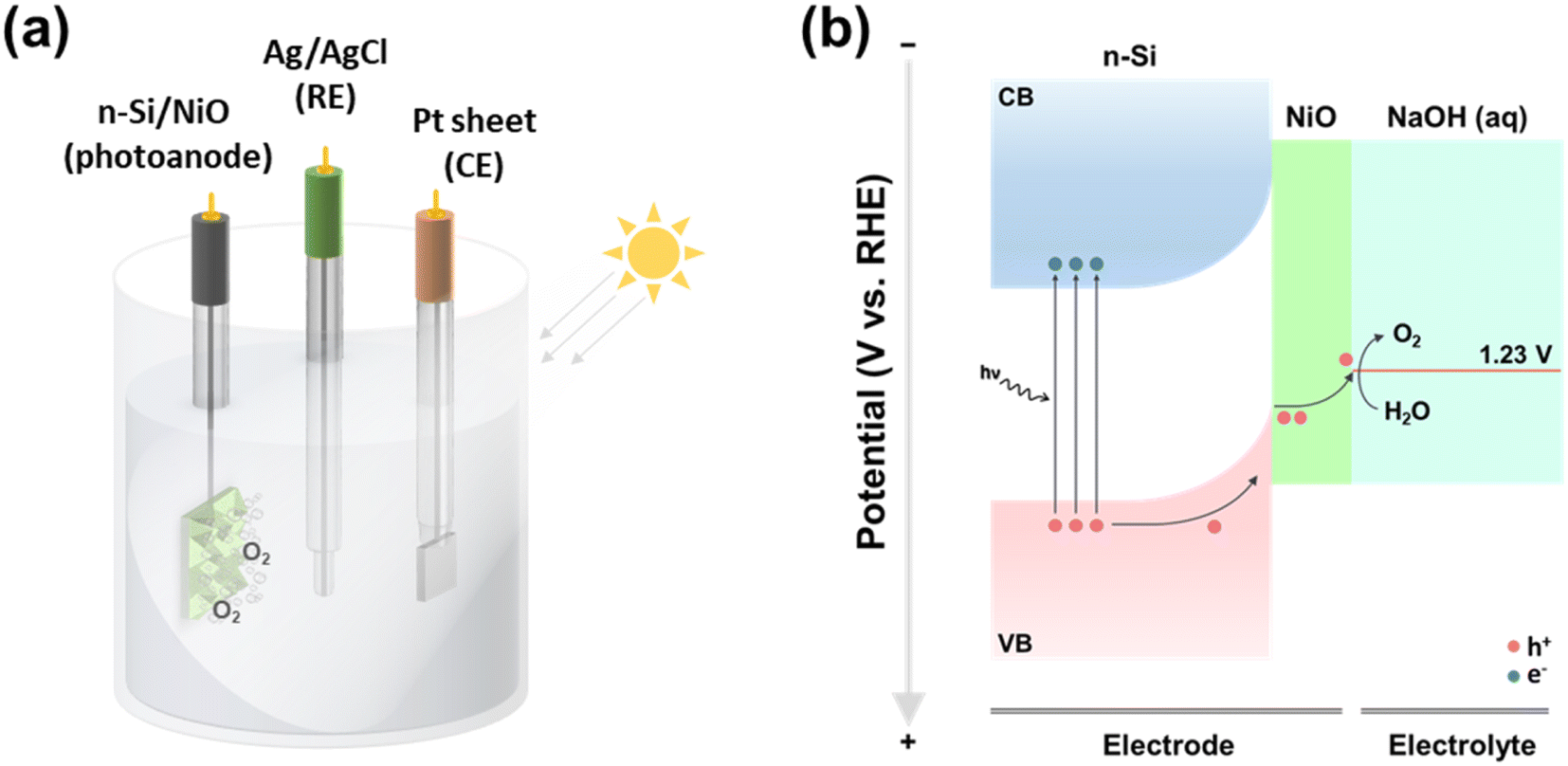 | ||
| Scheme 2 (a) Schematic illustration and (b) energy diagram of the n-Si/NiO photoanode-based photoelectrochemical cell (PEC). | ||
Based on the established annealing condition of 300 °C, NiO films were deposited by varying the coating time from 1 to 9 min to investigate the effect of film thickness and morphology on the photoelectrochemical performance while the morphology of the NiO films was characterized using scanning electron microscopy (SEM). As shown in Fig. 2a, increasing the dipping time in the CBD precursor solution resulted in a more pronounced porous structure and an increase in film thickness. This increase in porosity and thickness is presumably due to prolonged exposure to the precursor solution, leading to more nucleation sites and subsequent growth of NiO particles. Consequently, this morphological change led to a decrease in transmittance across the entire wavelength spectrum, as shown in the UV-Vis spectra (Fig. 2b). Note that thicker films absorb more light, reducing optical transparency and limiting the amount of light that reaches the underlying silicon photoanode.
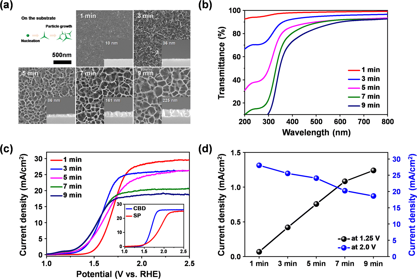 | ||
| Fig. 2 (a) Surface and cross-sectional SEM images and (b) optical transmittance of NiO films on n-Si substrates with various dipping time in the CBD precursor solution. Inset shows the suggested NiO growth/coating mechanism. (c) Plots of photocurrent density vs. voltage using NiO films on n-Si substrates with various dipping time in the CBD precursor solution. The inset shows plots of photocurrent density vs. voltage NiO films fabricated on n-Si substrates via CBD and spin-coating and (d) plots of extracted photocurrent densities at 1.25 V vs. RHE (left) and 2.0 V vs. RHE (right) using NiO films on n-Si substrates with various dipping time in the CBD precursor solution. Note that thermal annealing temperature was fixed at 300 °C. | ||
The effect of the CBD dipping/coating time on the photoelectrochemical catalytic performance of the resultant NiO/Si photoanode was examined by conducting the PEC analysis. As shown in Fig. 2c and d, as the coating time increased, the initial photocurrent at a lower voltage (1.25 V) also increased, indicating enhanced photocatalytic activity. This enhancement can be attributed to the increased catalytic surface area of the NiO film, which provides more active sites for the oxidation reaction. However, a trade-off was observed at higher voltages (>2 V), where the saturated photocurrent decreased with increasing coating time. This reduction in photoelectrochemical performance is possibly due to the decreased optical transmittance of the thicker NiO films (Fig. 2b), which limits light penetration into the underlying silicon substrate and reduces the total charge carrier generation. In the PEC system employing the NiO/n-Si photoanode, the NiO catalytic layer plays a dominant role at lower potentials, where its enhanced surface area facilitates water oxidation (i.e., oxygen evolution reaction). In contrast, at higher potentials, the n-Si acts as a photosensitized semiconductor, becoming more influential in achieving high saturation current density. Therefore, thicker NiO films, while beneficial for catalytic activity, may impede the overall photoelectrochemical performance by obstructing light penetration, which is crucial for the photo-response of the n-Si. Considering that optimizing the coating time is essential to achieve the optimal balance between the catalytic surface area and the optical transparency of NiO film, our findings confirm that the 3 min dipping in the CBD precursor solution leads to the NiO film which is thin enough to permit sufficient light penetration but still offers a substantially large catalytic surface area. Note that the NiO nanostructures prepared by CBD for 3 min followed by thermal annealing at 300 °C are sufficiently robust as confirmed by SEM images which showed no noticeable changes before and after PEC measurements (Fig. S1†). Additionally, it is noteworthy that the silicon photoanode with the NiO layer fabricated by the CBD method demonstrated more efficient photoelectrochemical catalytic performance than that with a NiO layer prepared by spin-coating of the sol–gel precursor solution (Fig. 2c inset). This result underscores the effectiveness of the CBD method in producing high-quality NiO films with superior photocatalytic properties.
Finally, we investigated the application of NiO films on 3D-structured silicon substrates to exploit the increased surface area enabled by KOH etching (see the Experimental section). As shown in Fig. 3a, the NiO layer was uniformly deposited onto the 3D-structured silicon substrates, indicating that the CBD method is viable for coating NiO films on substrates with complex surface topography. Fig. 3b illustrates the effect of this increased surface area on the photoelectrochemical performance. The 3D-structured silicon electrode with the NiO layer exhibited an increased on-set slope in the linear sweep voltammetry data at lower potentials, reflecting the enhanced catalytic activity due to the greater number of oxidation sites on the photoanode. Additionally, the 3D-structured silicon electrode showed a more significant increase in saturated current compared to the planar electrode, which can be attributed to the larger surface area provided by the NiO-coated silicon 3D structures. Finally, we successfully scaled up this approach to fabricate a large-area 3D-structured silicon photoanode with a NiO layer using the CBD method, as depicted in Fig. 3c. The NiO/n-Si (4-inch wafer) electrode effectively functioned as a photoanode for photoelectrochemical water splitting, with oxygen evolution observed across the entire surface under illumination (Fig. 3d and ESI Movie†). These results indicate that the solution-processed NiO film can serve as an effective passivation and catalytic layer for large-scale silicon photoanodes in PEC systems, providing both scalability and enhanced photocatalytic performance. These results demonstrate the potential of CBD-derived NiO films for practically useful application in large-scale PEC devices.
 | ||
| Fig. 3 (a) An SEM image of CBD NiO coating on the 3D-structured silicon substrate. (b) Plots of photocurrent density vs. voltage using NiO films deposited on 3D-structured (red) and planar (grey) n-Si substrates. (c) Optical photograph of CBD NiO coating on the 3D-structured 4-inch silicon substrate and (d) photoelectrochemical water splitting (oxygen bubbling) therein under light illumination (see also the ESI Movie†). | ||
Conclusions
In conclusion, this study demonstrates that NiO films prepared using chemical bath deposition can effectively serve as both protective and catalytic layers for silicon photoanodes in photoelectrochemical systems. By systematically varying annealing temperatures and coating times, we identified that an annealing temperature of 300 °C provides the optimal crystalline structure for NiO, balancing crystallinity with adequate surface area for catalytic activity. Furthermore, a CBD coating time of 3 minutes was found to produce NiO films that offer enhanced photocatalytic performance while maintaining sufficient optical transparency, outperforming films prepared by the sol–gel spin-coating method. The application of these optimized NiO films to 3D-structured silicon substrates further increased the active surface area, resulting in improved photoelectrochemical activity and higher saturation currents. Notably, we successfully scaled this approach to fabricate large-area 3D-structured silicon photoanodes with NiO layers, achieving efficient photoelectrochemical water splitting. These findings suggest that CBD-derived NiO films hold significant potential for large-scale, practical applications in PEC devices.Data availability
All data generated or analyzed during this study are included in this published article and its ESI.†Author contributions
The manuscript was written through contributions of all authors. All authors have given approval to the final version of the manuscript.Conflicts of interest
The authors declare no conflict of interest.Acknowledgements
This work was supported by the Ministry of Trade, Industry and Energy of Korea (RS-2024-00433822), the National Research Foundation (RS-2022-NR119715, RS-2020-NR045690, RS-2024-00341762), and GIST Research Institute (GRI) grant funded by the GIST in 2024.References
- M. Kiasari, M. Ghaffari and H. H. Aly, Energies, 2024, 17, 4128 CrossRef
.
- A. O. Ali, M. R. Elmarghany, M. M. Abdelsalam, M. N. Sabry and A. M. Hamed, J. Energy Storage, 2022, 50, 104609 CrossRef
- H. Zhang, Y. Lu, W. Han, J. Zhu, Y. Zhang and W. Huang, Chem. Eng. J., 2020, 393, 124766 CrossRef
- Y. Pan, H. Zhang, B. Zhang, F. Gong, J. Feng, H. Huang, S. Vanka, R. Fan, Q. Cao, M. Shen, Z. Li, Z. Zou, R. Xiao and S. Chu, Nat. Commun., 2023, 14, 1013 CrossRef PubMed
- B. Liu, S. Wang, G. Zhang, Z. Gong, B. Wu, T. Wang and J. Gong, Chem. Soc. Rev., 2023, 52, 4644–4671 RSC
- B. Moss, O. Babacan, A. Kafizas and A. Hankin, Adv. Energy Mater., 2021, 11, 2003286 CrossRef
- T. Yao, X. An, H. Han, J. Q. Chen and C. Li, Adv. Energy Mater., 2018, 8, 1800210 CrossRef
- J. H. Kim, D. Hansora, P. Sharma, J.-W. Jang and J. Sung Lee, Chem. Soc. Rev., 2019, 48, 1908–1971 RSC
- D. Li, J. Shi and C. Li, Small, 2018, 14, 1704179 CrossRef
- J.-B. Pan, S. Shen, L. Chen, C.-T. Au and S.-F. Yin, Adv. Funct. Mater., 2021, 31, 2104269 CrossRef
- W. Hong, Q. Cai, R. Ban, X. He, C. Jian, J. Li, J. Li and W. Liu, ACS Appl. Mater. Interfaces, 2018, 10, 6262–6268 CrossRef CAS
- X. Yu, P. Yang, S. Chen, M. Zhang and G. Shi, Adv. Energy Mater., 2017, 7, 1601805 CrossRef
- H. J. Fu, I. A. Moreno-Hernandez, P. Buabthong, K. M. Papadantonakis, B. S. Brunschwig and N. S. Lewis, Energy Environ. Sci., 2020, 13, 4132–4141 RSC
- D. Bae, B. Seger, P. C. K. Vesborg, O. Hansen and I. Chorkendorff, Chem. Soc. Rev., 2017, 46, 1933–1954 RSC
- X. Li, W. Lu, W. Dong, Q. Chen, D. Wu, W. Zhou and L. Chen, Nanoscale, 2013, 5, 5257–5261 RSC
- B. Mei, B. Seger, T. Pedersen, M. Malizia, O. Hansen, I. Chorkendorff and P. C. K. Vesborg, J. Phys. Chem. Lett., 2014, 5, 1948–1952 CrossRef PubMed
- S. A. Lee, T. H. Lee, C. Kim, M. G. Lee, M.-J. Choi, H. Park, S. Choi, J. Oh and H. W. Jang, ACS Catal., 2018, 8, 7261–7269 CrossRef
- I. A. Moreno-Hernandez, B. S. Brunschwig and N. S. Lewis, Adv. Energy Mater., 2018, 8, 1801155 CrossRef
- P. P. Sahoo, M. Mikolášek, K. Hušeková, E. Dobročka, J. Šoltýs, P. Ondrejka, M. Kemény, L. Harmatha, M. Mičušík and K. Fröhlich, ACS Appl. Energy Mater., 2021, 4, 11162–11172 CrossRef
- C. Ros, N. M. Carretero, J. David, J. Arbiol, T. Andreu and J. R. Morante, ACS Appl. Mater. Interfaces, 2019, 11, 29725–29735 CrossRef
- T. Han, Y. Shi, X. Song, A. Mio, L. Valenti, F. Hui, S. Privitera, S. Lombardo and M. Lanza, J. Mater. Chem. A, 2016, 4, 8053–8060 RSC
- M. J. Kenney, M. Gong, Y. Li, J. Z. Wu, J. Feng, M. Lanza and H. Dai, Science, 2013, 342, 836 CrossRef
- M. A. Mat-Teridi, A. Ali Tahir, S. Senthilarasu, K. G. U. Wijayantha, M. Y. Sulaiman, N. Ahmad-Ludin, M. A. Ibrahim and K. Sopian, Phys. Status Solidi RRL, 2014, 8, 982–986 CrossRef
- Z. Ying, X. Yang, R. Tong, Q. Zhu, T. Chen, Z. He and H. Pan, ACS Appl. Energy Mater., 2019, 2, 6883–6890 CrossRef
- C. Ros, T. Andreu, J. David, J. Arbiol and J. R. Morante, J. Mater. Chem. A, 2019, 7, 21892–21902 RSC
- F. Yang, X. Zhou, N. T. Plymale, K. Sun and N. S. Lewis, J. Mater. Chem. A, 2020, 8, 13955–13963 RSC
- K. Sun, N. Park, Z. Sun, J. Zhou, J. Wang, X. Pang, S. Shen, S. Y. Noh, Y. Jing, S. Jin, P. K. L. Yu and D. Wang, Energy Environ. Sci., 2012, 5, 7872–7877 RSC
- S.-Y. Han, D.-H. Lee, Y.-J. Chang, S.-O. Ryu, T.-J. Lee and C.-H. Chang, J. Electrochem. Soc., 2006, 153, C382–C386 CrossRef
- X. H. Xia, J. P. Tu, J. Zhang, X. L. Wang, W. K. Zhang and H. Huang, Sol. Energy Mater. Sol. Cells, 2008, 92, 628–633 CrossRef
- X. Xia, J. Tu, Y. Zhang, X. Wang, C. Gu, X.-b. Zhao and H. J. Fan, ACS Nano, 2012, 6, 5531–5538 CrossRef
Footnotes |
| † Electronic supplementary information (ESI) available. See DOI: https://doi.org/10.1039/d4ra06774f |
| ‡ These authors equally contributed to this research. |
| This journal is © The Royal Society of Chemistry 2024 |