DOI:
10.1039/D4RA04756G
(Paper)
RSC Adv., 2024,
14, 24226-24235
Wide-direct-band-gap monolayer carbon nitride CN2: a potential metal-free photocatalyst for overall water splitting
Received
30th June 2024
, Accepted 29th July 2024
First published on 5th August 2024
Abstract
Two dimensional metal-free semiconductors with high work function have attracted extensive research interest in the field of photocatalytic water splitting. Herein, we have proposed a kind of highly stable monolayer carbon nitride CN2 with an anisotropic structure based on first principles density functional theory. The calculations of electronic structure properties, performed using the HSE06 functional, indicate that monolayer CN2 has a wide direct band gap of 2.836 eV and a high work function of 6.54 eV. And the suitable band edge alignment, high electron mobility (∼103 cm2 V−1 s−1) and visible-light optical absorption suggest that monolayer CN2 has potential on visible-light photocatalytic water splitting at pH ranging from 0 to 14. Moreover, we have observed that uniaxial strain can effectively control the electronic structure properties and optical absorption of monolayer CN2, which can further improve its solar to hydrogen efficiency from 9.6% to 16.02% under 5% uniaxial tension strain along the Y direction. Our calculations have not only proposed a new type of potential metal-free photocatalyst for water splitting but also provided a functional part with high work function for type-I and scheme-Z heterojunction applied in photocatalytic water splitting.
1 Introduction
Two dimensional (2D) semiconductor photocatalysts applied in water splitting have received widespread research interest due to their high specific surface area and abundant reactive active sites caused by a unique atomic-scale thickness feature.1–6 Motivated by it, much attention has been drawn to exploring new 2D semiconductors for photocatalytic water splitting. For completely photocatalytic water splitting, 2D semiconductors should have suitable band edge alignment to satisfy the band structure requirement of photocatalytic water splitting, including band gaps being larger than 1.23 eV and the valence band maximum (VBM) and conduction band minimum (CBM) relative to the vacuum level being higher than the reduction potential (VH+/H2 = −4.44 eV) and lower than the oxidation potential (VOH−/O2 = −5.67 eV), respectively.7–10 In addition, to consider the pH ranging from 0 to 14, the band gaps of 2D semiconductor photocatalysts should be larger than 2.0 eV so as to guarantee the reduction reaction in photocatalytic water splitting.11–14 Furthermore, large enough overpotential and strong visible light optical absorption are also essential for ensuring enough driven energy and relatively high solar conversion efficiency. Based on the above, a comprehensive 2D semiconductor photocatalyst for water splitting should have a wide band gap (>2.0 eV), high work function and favourable optical absorption.15–19 Besides, a wide-band-gap 2D semiconductor with high work function can be adopted in type-II and Z-scheme van der Waals heterojunctions for photocatalytic water splitting.20–28 Therefore, it is necessary for exploring more wide-band-gap 2D semiconductor photocatalysts with high work function and excellent optical absorption for photocatalytic water splitting.
A 2D material with high work function always means that it owns strong ability for binding electrons. To design the 2D material with high work function, one of elements that have high electronegativity should be contained, such as C, N, O and S elements. Typically, 2D carbon nitrides with economic and clean features are hot candidates for the application of photocatalytic water splitting.29,30 2D g-C3N4, one of most famous 2D carbon nitrides, has wide direct band gap, strong optical absorption in visible-light region and suitable band edge alignment for photocatalytic water splitting.31–38 Besides, monolayer g-C2N is also reported that have potential in the application of photocatalytic water splitting.39 However, these two graphene-like 2D carbon nitrides do not own high enough work function, which is not beneficial for the oxidation reaction activity. Moreover, the graphene-like monolayer C3N and some others graphene-like 2D carbon nitrides have small band gaps,40,41 relative low work function and do not suitable for photocatalytic water splitting. The phenomenon is mainly cause by that the outmost electrons C atoms and even N atoms are not fully saturated. On the contrary, the monolayer C3N2 owning four-bonded C atoms (sp3 hybridization) and three-bonded N atoms (sp3 hybridization) exhibits wide band gap, pretty high work function (∼7.0 eV) and suitable band edges alignment for photocatalytic water splitting. Meanwhile, such the electronic structure properties of monolayer C3N2 reveals its great potential on being an important component in type-I and Z-scheme heterojunction for photocatalytic water splitting.42 Therefore, to explore the new 2D carbon nitrides with high work function and wide band gap, the sp3-C atoms and sp3-N atoms should be fully contained.
In this paper, we have theoretically designed a new type of 2D carbon nitrides called monolayer CN2 based on first-principles density functional theory (DFT). The stability of monolayer CN2 was confirmed by the calculations of cohesive energy, phonon spectrum and ab initio molecular dynamics (AIMD) at 300 K and 400 K. The electronic structure properties of monolayer CN2 were investigated through its band structure, density of state and work function, which indicated that monolayer CN2 was a wide-direct-band-gap semiconductor with high work function. Moreover, its carrier mobility, optical absorption, band edge alignment relative to the vacuum level and solar to hydrogen (STH) efficiency were further studied to preliminarily evaluate the photocatalytic ability of monolayer CN2 for water splitting. Finally, the uniaxial strain along X and Y direction were applied to monolayer CN2 to study the strain effect on electronic structure properties, optical absorption and photocatalytic properties.
2 Computational details
All results in this paper were carried out by performing the calculations based on first-principles density functional theory (DFT). The Vienna Ab Initio Simulation Package (VASP) was used for the calculation of geometry optimization, band structures and optical absorption. The projector-augmented-wave (PAW) pseudopotentials were utilized with a 500 eV plane-wave cutoff energy.43 The conventional cell of monolayer CN2 were mainly used considering its anisotropic structure feature. The Brillouin zone sampling adopted 12 × 8 × 1 gamma-centered k-point mesh.44 A vacuum separation between neighbouring monolayers was over 20 Å. The Perdew–Burke–Emzerh of Generalized Gradient Approximation (GGA + PBE) was used for geometry optimization.45 The monolayer CN2 were relaxed until the internal stress was reduced to below 0.001 eV Å−1, and the energy tolerance was set to be less than 1 × 10⁻⁸ eV per atom. The thermodynamic stability of monolayer CN2 at 300 K and 400 K was simulated through ab initio molecular dynamics (AIMD) with using 96 atoms supercell and NVT canonical ensemble.46 The total simulation time was set to 5 ps corresponding to 5000 simulation steps. The band structures and optical absorption spectra of monolayer CN2 were calculated by using the Heyd–Scuseria–Ernzerh of hybrid functional (HSE06).47 The VASPKIT code was used for post-processing data obtained from the VASP code.48 The phonon dispersion spectrum of monolayer CN2 was calculated using the linear response approach implemented in the Cambridge Series of Total Energy Package (CASTEP).49 For phonon spectrum calculations, norm-conserving pseudopotentials and a plane-wave cutoff energy of 750 eV were employed, while other settings were consistent with those used in the VASP code.
3 Results and discussion
3.1 The structure and stability of monolayer CN2
After sufficient structure optimization, the structure models of monolayer CN2 are given in Fig. 1. In the monolayer CN2, each C atom bond with two C atoms and two N atoms while each N atom bond with one C atom and two N atoms. It is clear that both the C and N atoms in the monolayer are sp3 hybridization, which means the structure reasonability of monolayer CN2. Learning from Fig. 1, we also can get that the structure of monolayer CN2 is anisotropic reflecting atom alignment difference between X direction and Y direction shown in Fig. 1(a). And in order to study the anisotropic properties of monolayer CN2 caused by its anisotropic structure, we carry out its conventional cell containing the lattice parameters, as shown in Fig. 1(d). Although the structure of monolayer CN2 seems to be reasonable, the further studies about its energy, dynamic and thermodynamic stability are still sorely necessary. For the energy stability, we have calculated the cohesive energy (Ecoh) of monolayer CN2 as followed formula:| |
 | (1) |
where Etot is the total energy of monolayer CN2, and the Eatom(C) and Eatom(N) are the energy of free C and N atoms, respectively. The calculation presents that the Ecoh of monolayer CN2 is −7.48 eV per atom, which is lower than that of monolayer C2N and g-C3N4. So we consider such Ecoh as an evidence for proving that monolayer CN2 is energy stable. In addition, we have carried out the phonon spectrum of monolayer CN2 that is shown in Fig. 2(a). It is noticed that there is not imaginary frequency in the phonon spectrum of monolayer CN2, which indicates that monolayer CN2 is dynamically stable. Moreover, the thermodynamic stability of monolayer CN2 have been investigated by performing the AIMD simulation at 300 K and 400 K, which represent the room temperature and the temperature of boiling water, respectively. The Fig. 2(b) exhibits that, during AIMD simulation at 300 K and 400 K, the total energy of monolayer CN2 do not have mutations and keep in a dynamic equilibrium process. Furthermore, the Fig. 2(c and d) present that, after 5 ps AIMD simulation at 300 K and 400 K, there are no dramatic changes in the structure of monolayer CN2. Therefore, we confirm that monolayer CN2 are thermodynamically stable at 300 K and 400 K.
 |
| | Fig. 1 (a) and (b) are the top and side view of monolayer CN2 after full optimization, respectively. (c) and (d) are the primitive cell and conventional cell of monolayer CN2, respectively. And the lattice parameters a, b and h of conventional cell are also exhibited (e) is the Brillouin zone containing main high symmetric points for the conventional cell of monolayer CN2. | |
 |
| | Fig. 2 (a) Is the phonon dispersion spectrum of monolayer CN2. (b) Presents the total energy change of monolayer CN2 in AIMD simulations at 300 K and 400 K. The (c) and (d) are the final structures of monolayer CN2 after the AIMD simulations at 300 K and 400 K, respectively. | |
3.2 The electronic structure, optical absorption and photocatalytic properties of monolayer CN2
The projected band structure of optimized monolayer CN2 were calculated by HSE06 hybrid function shown in Fig. 3(a and b). The Fig. 3(a and b) show that monolayer CN2 is a wide-direct-band-gap semiconductor with a 2.836 eV band gap. And both the VBM and CBM are locating at G point. The such band gap is similar with the band gap of g-C3N4. Comparing Fig. 3(a) with Fig. 3(b), we find that the states near the VBM and CBM are mainly contributed by N atoms while there is minor contribution from C atoms. To further study the atomic orbital occupation of monolayer CN2, we have calculated the projected density of states (PDOS), as shown in Fig. 4. The total density of states (TDOS) in the Fig. 4(a) indicates that the occupation peaks near the VBM and CBM are relatively low, which will be unfavorable for electron collective transition and lead to weak optical absorption in low energy region. The Fig. 4(a) also identify that the N atoms have major contribution on the states near the VBM and CBM and the situation of C atoms is opposite. Learning from Fig. 4(b and c), we find that the states near the VBM are mainly contributed by the pz orbital for C atoms and the pz orbital for N atoms. Additionally, the states near the CBM are mainly contributed by the pz orbital for C atoms and the s orbital for N atoms. Based on the situation, we suppose that carrier would tend to transfer in the Y direction. And the further calculation about carrier mobility along X direction and Y direction have been performed in the next section to identify the conjecture.
 |
| | Fig. 3 (a) and (b) Are projected band structures contributed by N atoms and C atoms, respectively. | |
 |
| | Fig. 4 (a) contain the TDOS of monolayer CN2 and the PDOS contribured from C atoms and N atoms. (b) is the orbit-resolved PDOS of C atoms. (c) is the orbit-resolved PDOS of N atoms. | |
The carrier mobility of monolayer CN2 were estimated by the 2D deformation potential (DP) theory with considering its anisotropic properties. The carrier mobility was calculated by following equations:50
| |
 | (2) |
| |
 | (3) |
| | |
C2D = 2[∂2E/∂(Δa/a0)2]/S0
| (4) |
| |
 | (5) |
where the
μ is the carrier mobility, the
C2D is the effective elastic modulus, The
T is 300 K, the
m* is effective mass along specific direction, the
md is average effective mass, and the
El is the deformation potential constants. For the
C2D, the
a0 is the lattice constant without strain, the Δ
a presents the deformation of
a0, the
S0 is the total area of structures without strain, and the
E is the total energy with the strain along specific direction. For the
El, the
Eedge is the change of the CBM and VBM with the strain along specific direction. The results are shown in
Table 1. We get that the electron mobility along
X direction and
Y direction are 88.4 and 754.1 cm
2 V
−1 s
−1, respectively. Additionally, the hole mobility along
X direction and
Y direction are 303.6 and 1009.2 cm
2 V
−1 s
−1. It can be observed that the carrier mobility along
Y direction is higher than that along
X direction, which confirms the above conjecture mentioned at the analysis of DOS. Moreover, there are relatively large differences between hole and electron mobility both along
X direction and
Y direction, which is conducive to the separation of photogenerated hole and electron in the photocatalytic process.
Table 1 The electron and hole effective masses  and
and  , elastic modulus C2D (eV Å−2), deformation energies El (eV) and carrier mobilities μ (cm2 V−1 s−1) for monolayer CN2 along X and Y directions at 300 K calculated by HSE06 hybrid functional
| |
mX |
mY |
El – X |
El – Y |
C2D – X |
C2D – Y |
μ2D – X |
μ2D – Y |
| e |
0.24 |
0.67 |
36.12 |
6.71 |
33.26 |
27.17 |
88.4 |
754.1 |
| h |
7.76 |
0.69 |
3.13 |
3.10 |
303.6 |
1009.2 |
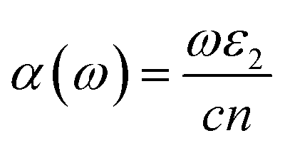
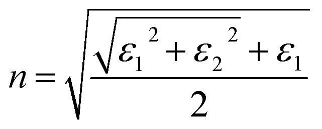
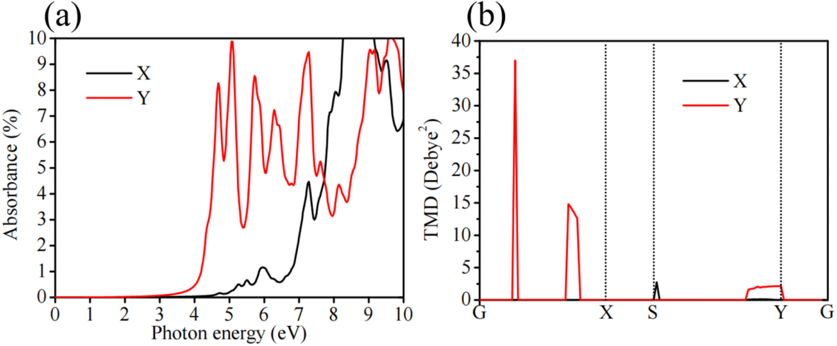
Due to the anisotropic electronic structure properties, the optical absorption properties of monolayer CN2 will logically present anisotropic. The optical absorption spectra of monolayer CN2 polarized in X direction and Y direction have been carried out by following formulas:
| |
 | (8) |
| |
 | (9) |
where
A(
ω) presents the optical absorbance,
α(
ω) presents the absorption coefficient, Δ
Z presents the primitive-cell size in the direction of vacuum layer,
n presents the index of refraction,
ε1 and
ε2 respectively present the real and imaginary parts of their dielectric function,
ω presents the incident light frequency,
c presents the speed of light in vacuum. The result are shown in
Fig. 5(a). It exhibits that monolayer CN
2 has optical absorption from violet region to ultraviolet region. In addition, we obtain that there exists anisotropic optical absorption reflecting on the optical absorption polarized in
Y direction having much smaller optical gap and being much stronger in the region from ∼3.0 eV to ∼7.0 eV compared with that polarized in
X direction. To explain the phenomenon, we then have calculated the transition dipole moment between highest VB and lowest CB presented in
Fig. 5(b). It is well known that the higher transition dipole moment always reveals stronger optical absorption. The
Fig. 5(b) indicates that, when it is near VBM, the transition dipole moment along
Y direction is very high while the transition dipole moment along
X direction is very low, which can support the anisotropic optical absorption of monolayer CN
2.
 |
| | Fig. 5 (a) and (b) Are the optical absorption spectrum and transition dipole moment of monolayer CN2, respectively. | |
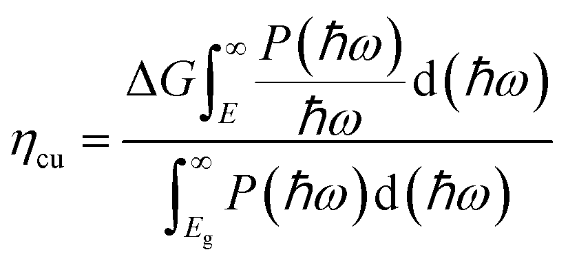
For further studying the photocatalytic properties of monolayer CN2 for water splitting, its band edges alignment relative to vacuum level (VL) have been carried out after calculating its work function. And then, the VBM and CBM relative to VL have been compared with the H+/H2 reduction potential [V(H+/H2) = −4.44 eV + PH × 0.059 eV] and the OH−/O2 oxidation potential [V(OH−/O2) = −5.67 eV + PH × 0.059 eV] with considering the influence of PH values ranging from 0 to 14, as shown in Fig. 6(a). It presents that, when the PH values are ranging from 0 to 14, the VBM is higher than the V(H+/H2) and the CBM is lower than the V(OH−/O2), which means that monolayer CN2 has potential on overall photocatalytic water splitting. In addition, it also exhibits that, with the increase of PH values, the overpotential χ(H2) for H+/H2 reduction will decrease and while the overpotential χ(O2) for the OH−/O2 oxidation will increase. Moreover, when the PH value is 7 corresponding to neutral water, the χ(H2) and χ(O2) are 0.37 eV and 1.24 eV, respectively, which indicates that monolayer CN2 would have good photocatalytic activity in water splitting at PH = 7. As the band gap, χ(H2) and χ(O2) of monolayer CN2 with considering PH values ranging from 0 to 14 were obtained, the corresponding solar to hydrogen (STH) efficiency have been calculated by following formulas:
 |
| | Fig. 6 (a) Is the VBM and CBM of monolayer CN2 comparing with the redox potential water splitting at PH ranging from 0 to 14. (b) Is the optical absorption ηab, carrier utilization ηcu, solar to hydrogen ηsth efficiency changing with the PH values. | |
The optical absorption efficiency (ηab):51–53
| |
 | (10) |
where the
Eg is the band gap, and
P(
ħω) is the AM 1.5G solar energy flux as functional of the photon energy
ħω.
The efficiency of carrier utilization (ηcu):
| |
 | (11) |
where the Δ
G is 1.23 eV describing the potential difference of water splitting, and
E is the photon energy actually used for water splitting, which is defined as:
| |
 | (12) |
The STH efficiency (ηsth):
The results, including the ηab, ηcu and ηsth, are shown in Fig. 6(b). Learning from the Fig. 6(b), we can get that, when the PH = 0, 1 and 2, the ηsth have maximum values 9.6% for ηsth. And then, with the increase of PH values from 3 to 14, the ηsth will reduce. For instance, when PH = 7 and 14, the ηsth are 5.8% and 2.4%, respectively. The phenomenon is caused by that, when the PH values are ranging from 3 to 14, the values of ηab will not be affected but the values of ηcu will decrease with the increase of PH values due to the χ(H2) and χ(O2) changing with the PH but the band gap not.
3.3 The strain effect on the band structure, optical absorption and photocatalytic properties of monolayer CN2
Although the STH efficiency of monolayer CN2 reach 9.6% at PH = 0, the performance of monolayer CN2 in photocatalytic water splitting does not satisfy the requirement of economic hydrogen production, which needs the STH efficiency of photocatalysts beyond 10%. Thus, we have applying the uniaxial strain along X and Y direction to monolayer CN2 shown in Fig. 7(a), which is expected to improve the photocatalytic ability of monolayer CN2 in water splitting. The strain with negative sign represents compressive strain while the strain with positive sign means tension strain. The magnitude of strain means the ratio of the deformation of lattice parameter (a or b) to the original value. The Fig. 7(b) reveals the relation of stress to uniaxial strain, which can give a guide to the relevant experiment. Learning from Fig. 7(b), we find that the hardness of monolayer CN2 along X direction is higher than that along Y direction and the tension strain is easier to achieve in monolayer CN2 rather than compressive strain. In addition, it also exhibits that, under the compressive strain, the stress varies linearly, which means the potential of monolayer CN2 on pressure sensors.
 |
| | Fig. 7 (a) Is the schematic diagram for applying uniaxial strain to monolayer CN2. (b) Is the stress of monolayer CN2 changing with strain. | |
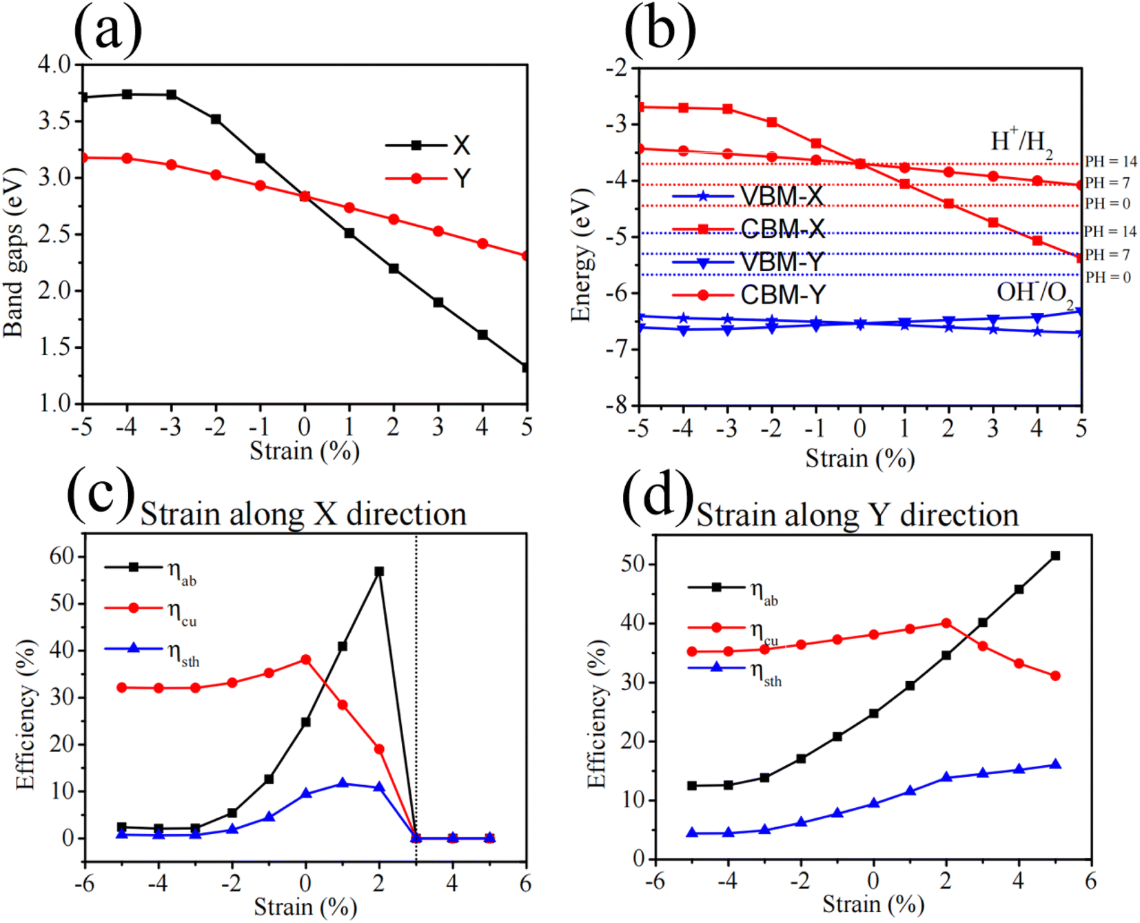
To study the strain effect on the photocatalytic properties of monolayer CN2 in water splitting, we have first carried out the band structures that change with the uniaxial strain along X and Y direction. The Fig. 8(a) exhibits the band gaps of monolayer monolayer CN2 changing with the strain. It shows that, when the strain is ranging from −5% to 5% along X direction, the band gaps of monolayer CN2 can be tuned from 1.322 eV to 3.713 eV. And when the strain is ranging from −5% to 5% along Y direction, the band gaps can be tuned from 2.309 eV to 3.178 eV. The phenomenon indicates that, compared with the strain along Y direction, the strain along X direction can more effectively control the band gap of monolayer CN2 due to the VBM and CBM being mainly contributed by N atoms. In addition, when the strain is ranging from −3% to 5% either along X or Y direction, the variation trend of band gap is near-linear, which will facilitate the regulation according to the need of practical application. Furthermore, as shown in Fig. 8(b), we also have carried out the band edge alignment of monolayer CN2 with the uniaxial strain. Compared with the oxidation reduction potential in water splitting at PH = 0, 7 and 14, we find that, with uniaxial strain compressive ranging from −5% to 0 whether along X and Y direction, the monolayer CN2 still can satisfy the band structure requirement of photocatalytic water splitting at PH ranging from 0 to 14. When the uniaxial strain is tension along X direction, monolayer CN2 can keep its photocatalytic ability in water splitting under 0–2% strain at PH = 0 and 0–1% strain at PH = 7. Additionally, under the 0–5% uniaxial tension strain along Y direction, monolayer CN2 can keep its photocatalytic ability in water splitting at PH = 0 and PH = 7. Moreover, the Fig. 8(b) also indicates that, at PH = 14, the uniaxial tension strain whether along X and Y direction would make monolayer CN2 not suitable for photocatalytic water splitting.
 |
| | Fig. 8 (a) Is the band gaps of monolayer CN2 changing with uniaxial strain. (b) Is the VBM and CBM of monolayer CN2 under the uniaxial strain, comparing with the redox potential water splitting at P = 0, 7 and 14. (c) and (d) are the ηab, ηcu and ηsth of monolayer CN2 under uniaxial strain along X and direction, respectively. | |
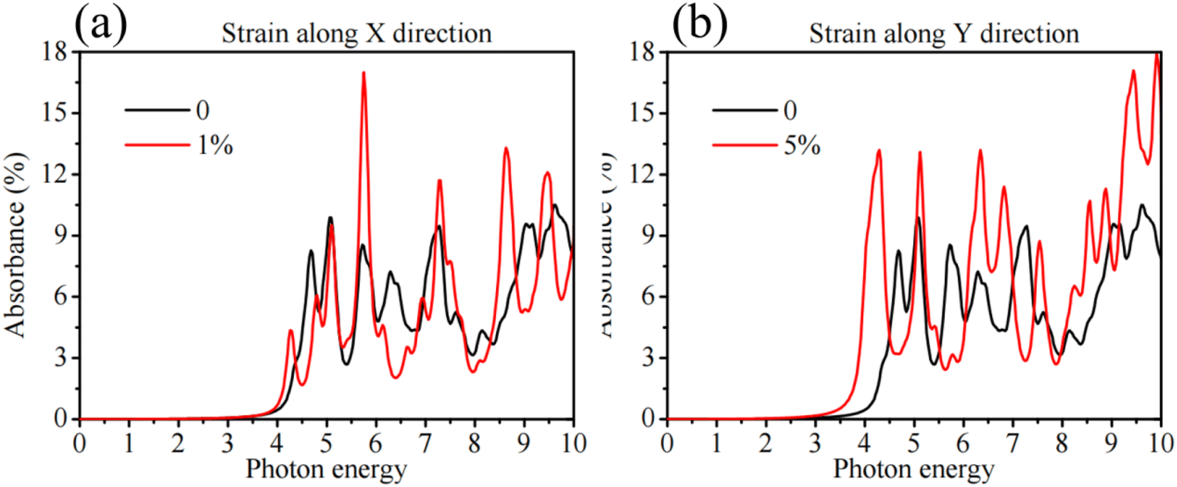
The ηab, ηcu and ηsth of monolayer CN2 at PH = 0 have been presented in Fig. 8(c and d) after obtaining the change of the band gap, χ(H2) and χ(O2) with the uniaxial strain. As shown in Fig. 8(c), although the ηab and ηcu are not the highest values under 1% uniaxial tension strain along X direction, the monolayer CN2 has optimal ηsth reaching 11.64%, which means that applying 1% uniaxial tension strain can make monolayer CN2 own potential on economic hydrogen production. In addition, when it is uniaxial tension strain ranging from 1% to 5% along Y direction, the ηsth of monolayer CN2 is beyond the 10% and increases with the increase of uniaxial tension strain. And under 5% uniaxial tension strain along Y direction, the ηsth of monolayer CN2 can be up to 16.02%. Furthermore, we also have carried out the optical absorption spectra of monolayer CN2 with 1% uniaxial tension strain along X direction and 5% uniaxial tension strain along Y direction, which make monolayer CN2 have pretty ηsth. As shown in Fig. 9(a), under the 1% uniaxial tension strain along X direction, the optical absorption polarized along Y direction of monolayer CN2 is red shift compared with that without strain. And the Fig. 9(b) shows that, with the 5% uniaxial tension strain along Y direction, the optical absorption of monolayer CN2 is red shift and its first absorption peak become stronger than that without strain. Above phenomenons suggest that applying suitable uniaxial tension strain to monolayer CN2 can effective improve the photocatalytic ability of monolayer CN2 in water splitting.
 |
| | Fig. 9 (a) Is the optical absorption spectrum of monolayer CN2 under 1% uniaxial tension strain along X direction comparing with that of monolayer CN2 without strain. (b) Is the optical absorption spectrum of monolayer CN2 under 5% uniaxial tension strain along Y direction comparing with that of monolayer CN2 without strain. | |
4 Conclusion
In summary, we have theoretically proposed a kind of anisotropic monolayer carbon nitride – CN2 via first-principles DFT. Through the calculations of cohesive energy, phonon dispersion spectrum and AIMD simulations at 300 K and 400 K, we confirm that monolayer CN2 has high stability in energy, dynamics and thermodynamics. By using HSE06 functional, we find that monolayer CN2 is wide-direct-band-gap semiconductor with 2.836 eV band gap. And it also exhibit that its band edge alignment relative to vacuum level satisfy the requirement of photocatalysts applied in water splitting at PH ranging from 0 to14. And the efficiency of solar to hydrogen in monolayer CN2 is 9.6% at PH = 0. Due to the anisotropic structure, the monolayer CN2 has anisotropic carrier mobility and optical absorption. And our calculations present that monolayer CN2 has high electron mobility (∼103 cm2 V−1 s−1) and visible-ligh optical absorption along Y direction while that along X direction own poor performances. Finally, we have studied the uniaxial strain effect on the electronic, optical and photocatalytic properties of monolayer CN2. And the results show that uniaxial strain can effectively tune the band gap, overpotential and optical absorption of monolayer CN2, which can further control the photocatalytic ability for water splitting. Our calculations not only propose a kind of wide-direct-band-gap semiconductor for photocatalytic water splitting but also provide a potential functional component for forming type-I and scheme-Z heterojunction applied in photocatalytic water splitting.
Data availability
The data that support the findings of this study are available on request from the corresponding author “Jiahe Lin”upon reasonable request.
Conflicts of interest
There are no conflicts to declare.
Acknowledgements
This study was supported by the National Natural Science Foundation of China (Grant No. 12204195) and the Fujian Province Department of Science and Technology (China) (Grant No. 2020J05147).
References
- M. Z. Rahman, C. W. Kwong, K. Davey and S. Z. Qiao, Energy Environ. Sci., 2016, 9, 709–728 RSC
 .
. - S. Mekhilef, R. Saidur and A. Safari, Renew. Sustain. Energy Rev., 2011, 15, 1777–1790 CrossRef .
- M. Pelaez, N. T. Nolan, S. C. Pillai, M. K. Seery, P. Falaras, A. G. Kontos, P. S. M. Dunlop, J. W. J. Hamilton, J. A. Byrne, K. O'Shea, M. H. Entezari and D. D. Dionysiou, Appl. Catal., B, 2012, 125, 331–349 CrossRef CAS .
- J. S. Lee, Catal. Surv. Asia, 2005, 9, 217–227 CrossRef CAS .
- B. Luo, G. Liu and L. Wang, Nanoscale, 2016, 8, 6904–6920 RSC .
- T. Hisatomi, J. Kubota and K. Domen, Chem. Soc. Rev., 2014, 43, 7520–7535 RSC .
- Z. Saleem, E. Pervaiz, M. U. Yousaf and M. B. K. Niazi, Catalysts, 2020, 10, 464 CrossRef CAS .
- N. Kannan and D. Vakeesan, Renew. Sustain. Energy Rev., 2016, 62, 1092–1105 CrossRef .
- Y. Li, Y.-L. Li, B. Sa and R. Ahuja, Catal. Sci. Technol., 2017, 7, 545–559 RSC .
- T. Su, Q. Shao, Z. Qin, Z. Guo and Z. Wu, ACS Catal., 2018, 8, 2253–2276 CrossRef CAS .
- N. Fajrina and M. Tahir, Int. J. Hydrogen Energy, 2019, 44, 540–577 CrossRef CAS .
- A. K. Singh, K. Mathew, H. L. Zhuang and R. G. Hennig, J. Phys. Chem. Lett., 2015, 6, 1087–1098 CrossRef CAS PubMed .
- K. Wenderich and G. Mul, Chem. Rev., 2016, 116, 14587–14619 CrossRef CAS PubMed .
- Q. Cai, M. Paulose, O. K. Varghese and C. A. Grimes, J. Mater. Res., 2005, 20, 230–236 CrossRef CAS .
- M. Z. Rahman, C. W. Kwong, K. Davey and S. Z. Qiao, Energy Environ. Sci., 2016, 9, 709–728 RSC .
- J. K. Stolarczyk, S. Bhattacharyya, L. Polavarapu and J. Feldmann, ACS Catal., 2018, 8, 3602–3635 CrossRef CAS .
- C.-F. Fu, J. Sun, Q. Luo, X. Li, W. Hu and J. Yang, Nano Lett., 2018, 18, 6312–6317 CrossRef CAS PubMed .
- Z. Guo, J. Zhou, L. Zhu and Z. Sun, J. Mater. Chem. A, 2016, 4, 11446–11452 RSC .
- X. Yang and D. Wang, ACS Appl. Energy Mater., 2018, 1, 6657–6693 CrossRef CAS .
- V. Soni, P. Raizada, A. Kumar, V. Hasija, S. Singal, P. Singh, A. Hosseini-Bandegharaei, V. K. Thakur and V.-H. Nguyen, Environ. Chem. Lett., 2021, 19, 1065–1095 CrossRef CAS .
- N. Fajrina and M. Tahir, Int. J. Hydrogen Energy, 2019, 44, 540–577 CrossRef CAS .
- S. Cao, X. Yan, Z. Kang, Q. Liang, X. Liao and Y. Zhang, Nano Energy, 2016, 24, 25–31 CrossRef CAS .
- S. Wang, J. Zhang, B. Li, H. Sun and S. Wang, Energy Fuels, 2021, 35, 6504–6526 CrossRef CAS .
- S. Nayak, G. Swain and K. Parida, ACS Appl. Mater. Interfaces, 2019, 11, 20923–20942 CrossRef CAS PubMed .
- F. K. Kessler, Y. Zheng, D. Schwarz, C. Merschjann, W. Schnick, X. Wang and M. J. Bojdys, Nat. Rev. Mater., 2017, 2, 17030 CrossRef CAS .
- X. Li, R. Shen, S. Ma, X. Chen and J. Xie, Appl. Surf. Sci., 2018, 430, 53–107 CrossRef CAS .
- W.-J. Ong, L.-L. Tan, Y. H. Ng, S.-T. Yong and S.-P. Chai, Chem. Rev., 2016, 116, 7159–7329 CrossRef CAS PubMed .
- A. Mehtab, S. Banerjee, Y. Mao and T. Ahmad, ACS Appl. Mater. Interfaces, 2022, 14, 44317–44329 CrossRef CAS PubMed .
- D. Zhao, Y. Wang, C.-L. Dong, Y.-C. Huang, J. Chen, F. Xue, S. Shen and L. Guo, Nat. Energy, 2021, 6, 388–397 CrossRef CAS .
- A. Alarawi, V. Ramalingam and J.-H. He, Mater. Today Energy, 2019, 11, 1–23 CrossRef CAS .
- J. Wen, J. Xie, X. Chen and X. Li, Appl. Surf. Sci., 2017, 391, 72–123 CrossRef CAS .
- D. Zhao, Y. Wang, C.-L. Dong, Y.-C. Huang, J. Chen, F. Xue, S. Shen and L. Guo, Nat. Energy, 2021, 6, 388–397 CrossRef CAS .
- L. Lin, Z. Yu and X. Wang, Angew. Chem., Int. Ed., 2019, 58, 6164–6175 CrossRef CAS PubMed .
- P. Niu, L. Zhang, G. Liu and H.-M. Cheng, Adv. Funct. Mater., 2012, 22, 4763–4770 CrossRef CAS .
- Z. Zhao, Y. Sun and F. Dong, Nanoscale, 2015, 7, 15–37 RSC .
- S. Cao, J. Low, J. Yu and M. Jaroniec, Adv. Mater., 2015, 27, 2150–2176 CrossRef CAS PubMed .
- X. Cai, Z. Zhu, W. Yu, C. Niu, J. Wang, B. Wang, X. Li, L. Zhang, R. Zhao and Y. Jia, Materials, 2018, 11, 1937 CrossRef PubMed .
- N. Wang, G. Yang, H. Wang, R. Sun and C.-P. Wong, Front. Chem., 2018, 6, 440 CrossRef CAS PubMed .
- J. Tian, Z. Zhou, S. Zhang, Z. Li, L. Shi, Q. Li and J. Wang, J. Mater. Chem. A, 2021, 9, 11753–11761 RSC .
- L.-B. Shi, Y.-Y. Zhang, X.-M. Xiu and H.-K. Dong, Carbon, 2018, 134, 103–111 CrossRef CAS .
- X. Zhou, W. Feng, S. Guan, B. Fu, W. Su and Y. Yao, J. Mater. Res., 2017, 32, 2993–3001 CrossRef CAS .
- J. Lin, T. Zhang, B. Zhang and X. Wang, Appl. Surf. Sci., 2021, 542, 148597 CrossRef CAS .
- G. Kresse and J. Furthmüller, Phys. Rev. B: Condens. Matter Mater. Phys., 1996, 54, 11169 CrossRef CAS PubMed .
- H. J. Monkhorst and J. D. Pack, Phys. Rev. B: Solid State, 1977, 16(4), 1748–1749 CrossRef .
- J. P. Perdew, K. Burke and M. Ernzerhof, Phys. Rev.
Lett., 1996, 77, 3865 CrossRef CAS PubMed .
- W. G. Hoover and B. L. Holian, Phys. Lett. A, 1996, 211, 253–257 CrossRef CAS .
- J. Heyd, G. E. Scuseria and M. Ernzerhof, Hybrid functionals based on a screened Coulomb potential, J. Chem. Phys., 2003, 118, 8207–8215 CrossRef CAS .
- V. Wang, N. Xu, J.-C. Liu, G. Tang and W.-T. Geng, Comput. Phys. Commun., 2021, 267, 108033 CrossRef CAS .
- M. D. Segall, P. J. D. Lindan, M. J. Probert and C. J. Pickard, J. Phys.: Condens. Matter, 2002, 14, 2717–2744 CrossRef CAS .
- K. Kaasbjerg, K. S. Thygesen and K. W. Jacobsen, Phys. Rev. B: Condens. Matter Mater. Phys., 2012, 85, 115317 CrossRef .
- M. Sun and U. Schwingenschlögl, Chem. Mater., 2020, 32, 4795–4800 CrossRef CAS .
- C.-F. Fu, J. Sun, Q. Luo, X. Li, W. Hu and J. Yang, Nano Lett., 2018, 18, 6312–6317 CrossRef CAS PubMed .
- J. Lin, T. Zhang, B. Zhang and X. Wang, Appl. Surf. Sci., 2021, 542, 148597 CrossRef CAS .
|
| This journal is © The Royal Society of Chemistry 2024 |
Click here to see how this site uses Cookies. View our privacy policy here. 
 Open Access Article
 This Open Access Article is licensed under a Creative Commons Attribution-Non Commercial 3.0 Unported Licence
 *a
*a


 and
and  , elastic modulus C2D (eV Å−2), deformation energies El (eV) and carrier mobilities μ (cm2 V−1 s−1) for monolayer CN2 along X and Y directions at 300 K calculated by HSE06 hybrid functional