
 Open Access Article
 This Open Access Article is licensed under a Creative Commons Attribution-Non Commercial 3.0 Unported Licence
From molecular salt to layered network: cation-driven tuning of band gap, structure, and charge transport in A3Bi2I9 (A = Cs, Rb) perovskites†
Mohamed Bouzidi*ab,
Mohamed Ben Bechir *c,
Dhaifallah R. Almalawid,
Idris H. Smailie and
Fahad Aljuaidf
*c,
Dhaifallah R. Almalawid,
Idris H. Smailie and
Fahad Aljuaidf
aDepartment of Physics, College of Science, University of Ha'il, P.O. Box 2440, Hail, Saudi Arabia. E-mail: m.bouzidi@uoh.edu.sa
bLaboratoire de Recherche sur les Hétéro-Epitaxies et Applications, Faculty of Science of Monastir, University of Monastir, Monastir 5000, Tunisia
cLaboratory of Spectroscopic and Optical Characterization of Materials (LaSCOM), Faculty of Sciences, University of Sfax, BP1171 – 3000 Sfax, Tunisia. E-mail: mohamedbenbechir@hotmail.com
dDepartment of Physics, College of Science, Taif University, Taif 21944, Saudi Arabia
eDepartment of Electrical and Electronic Engineering, College of Engineering and Computer Science, Jazan University, P. O. Box 114, Jazan 45142, Saudi Arabia
fApplied College at Mahayel Asir, King Khalid University, Abha, Saudi Arabia
First published on 22nd July 2024
Abstract
The increasing demand for eco-friendly and stable optoelectronic materials has led to interest in all-inorganic lead-free halide perovskites. This study reports the synthesis of A3Bi2I9 (A = Cs, Rb) perovskites via a solvothermal technique. The materials crystallize in hexagonal and monoclinic structures, with micrometer-sized particles. Optical investigations reveal direct band-gaps of 2.03 eV for Cs3Bi2I9 and 1.90 eV for Rb3Bi2I9. Raman spectroscopy highlights distinct vibrational modes, influenced by their structural differences. Space charge limited current (SCLC) measurements indicate varying threshold voltages and trap densities. Impedance spectroscopy and Jonscher's power law analysis reveal different polaron tunneling mechanisms in each compound. Ultrafast transient absorption spectroscopy shows the formation of self-trapped states upon photoexcitation, linked to lattice distortion and the formation of small polarons, which affect electrical conductivity.
1. Introduction
The burgeoning demand for environmentally sustainable and stable optoelectronic materials has prompted intensive exploration into lead-free alternatives, particularly in the realm of halide perovskites.1–10 Among these, all-inorganic lead-free halide perovskites have emerged as promising candidates owing to their potential for high performance and reduced environmental impact.11–13 These materials have shown versatility beyond traditional applications, including their potential utility in advanced X-ray detection technologies. For instance, white emission metal halides derived from all-inorganic perovskites offer advantages such as flexibility and transparency, making them promising candidates for next-generation X-ray scintillators.14 Additionally, one-dimensional CsCu2I3 single-crystal X-ray detectors have shown remarkable sensitivity and efficiency, highlighting the diverse applications of inorganic perovskites in radiation detection.15In this study, we delve into the influence of monovalent cations on the conduction mechanism in lead-free A3Bi2I9 perovskites (A = Cs, Rb).16,17 The choice of Cs and Rb as the monovalent cations stems from their distinct properties, which can profoundly affect the structural and electrical characteristics of the perovskite materials.18,19 Understanding these effects is pivotal for tailoring the properties of lead-free perovskites to suit specific applications. The synthesis of A3Bi2I9 perovskites was accomplished via the solvothermal technique, employing a meticulously controlled slow cooling process.20 Characterization techniques, including powder X-ray diffraction (PXRD) and scanning electron microscopy (SEM), provided insights into the structural and morphological features of the synthesized materials. Optical investigations, such as UV-Vis spectroscopy, unveiled direct band-gap values, while Raman spectroscopy shed light on vibrational modes characteristic of the crystal structures. Exploration of the charge transport mechanisms in A3Bi2I9 perovskites encompassed SCLC measurements and impedance spectroscopy. These techniques facilitated the elucidation of carrier mobility, trap densities, and contributions from grains and grain boundaries to the total impedance. Jonncher's power law analysis was instrumental in identifying the presence of overlapping large polaron tunneling mechanisms in Cs3Bi2I9 and non-overlapping small polaron tunneling mechanisms in Rb3Bi2I9, thereby elucidating the charge transportation mechanisms in these lead-free halide perovskites. Furthermore, a comparative analysis of the optical and electrical properties of Cs3Bi2I9 and Rb3Bi2I9 highlighted the structural disparities between the two compounds. Cs3Bi2I9, with its zero-dimensional (0D) molecular salt crystal structure, exhibited distinct optical properties compared to Rb3Bi2I9, which featured 2D layered derivatives of the perovskite structure. These structural variances significantly influenced the bandgap and electronic confinement, consequently impacting the electrical conductivity of the materials.
In conclusion, this study contributes to the understanding of the intricate interplay between monovalent cations, crystal structure, and functional properties in lead-free A3Bi2I9 perovskites. The elucidated insights offer valuable guidance for the design and optimization of lead-free perovskite materials for diverse optoelectronic applications, underscoring the significance of environmentally sustainable materials in advancing modern technology.
2. Experimental section
2.1. Materials
Cesium iodide (purity: 99.999%, Sigma-Aldrich), rubidium iodide (purity: 99.9%, Sigma-Aldrich), bismuth(III) iodide (purity: ≥99.998%, Sigma-Aldrich), and hydroiodic acid (purity: 99.99%, contains no stabilizer, distilled, 57 wt% in H2O, Sigma-Aldrich) were used in their as-received state for the experiments.2.2. Synthesis
A3Bi2I9 (where A = Cs, Rb) single crystals were grown via the solvothermal method, implementing a carefully controlled slow cooling procedure as depicted in Fig. 1. Instead of relying on natural cooling, the temperature of the precursor solution was gradually decreased from 180 °C to room temperature at a controlled rate of 1 °C per hour, following established protocols.4 | ||
| Fig. 1 Unveiling the solvothermal route to A3Bi2I9 (A = Cs, Rb) single crystals: a schematic depiction. | ||
2.3. Characterization
A3Bi2I9 (A = Cs, Rb) powders were characterized using Cu Kα radiation (λ = 1.54 Å) via PXRD at room temperature on a Rigaku MiniFlex 600 benchtop diffractometer. The analysis covered a 2θ range of 5°–40° with a step size of 0.02°.The morphology of A3Bi2I9 (A = Cs, Rb) powders was investigated using SEM. The analysis was performed with a Philips XL30 microscope operated at an accelerating voltage of 20 kV.
Thermogravimetric analysis (TGA) was employed to investigate the thermal decomposition behavior of powders derived from A3Bi2I9 (A = Cs, Rb) single crystals. The analysis was conducted using a PerkinElmer Pyris 6 instrument. The samples were heated at various heating rates, ranging from 0 to 800 °C, within a closed, perforated aluminum pan.
The diffuse reflectance of A3Bi2I9 (A = Cs, Rb) single crystals was measured in the ultraviolet-visible (UV-Vis) region using a PerkinElmer Lambda 950 spectrophotometer. The analysis was conducted at room temperature. The thicknesses of the single crystals of Cs3Bi2I9 and Rb3Bi2I9 are 0.93 mm and 0.87 mm, respectively.
Raman spectra of A3Bi2I9 (A = Cs, Rb) single crystals were collected at room temperature using a Horiba-Jobin-Yvon T64000 multi-channel spectrometer. The excitation source for the analysis was a laser operating at a wavelength of 785 nm.
Current–voltage (I–V) characteristics of A3Bi2I9 (A = Cs, Rb) were measured using a Keithley 2400 Source Meter.
The AC conductivity of A3Bi2I9 (A = Cs, Rb) pellets was investigated using a TH2828A impedance analyzer. Measurements were conducted at various frequencies ranging from 10 to 106 Hz with an applied AC voltage of 0.5 V. To explore the temperature dependence of conductivity, the samples were subjected to a heating ramp from 300 to 400 K at a rate of 4 K min−1 controlled by a TP94 temperature controller (Linkam, Surrey, UK).
This work employed the Helios pump-probe ultrafast spectroscopy system for conducting time-resolved measurements known as transient absorption (TA) spectroscopy. The Helios system comprises several key components:
• Laser source: A Ti:sapphire-based laser oscillator (Coherent Micra) acts as the initial light source.
• Amplification: The laser pulse energy is then amplified using a Coherent Legend amplifier.
• Pulse shaping: An optical parametric amplifier (OPA) equipped with a barium borate (BBO) crystal allows for shaping the laser pulse characteristics for optimal TA measurements.
The amplifier within the Helios system generates a near-Gaussian shaped laser pulse with a duration of around 35 femtoseconds (fs). This ultrashort pulse is centered at a wavelength of 700 nanometers (nm) and delivers an average power of 3.5 Watts (W) at a repetition rate of 1 kHz. Following amplification, the laser beam undergoes a precise splitting process. Approximately 70% of the beam's power is directed towards the optical parametric amplifier (OPA) for further manipulation. The remaining 30% of the beam is directed towards the spectrometer for potential reference or analysis. A critical component of the setup is a delay stage, capable of introducing a precise time delay within a range of 0 to 8 nanoseconds (ns) between the two split portions of the amplified laser beam. This time delay allows the 30% portion to act as a “probe beam” for subsequent spectroscopic analysis. To generate a suitable probe beam, the split beam is directed through a sapphire plate. This process creates a broad spectrum of light, known as a white-light continuum (WLC), encompassing wavelengths ranging from 375 to 750 nanometers (nm). This WLC serves as the ideal probe for the spectroscopic analysis. The highly stable output from the optical parametric amplifier (OPA) provided the pump beam for the experiment. This beam operated at a wavelength near 350 nanometers (nm) and delivered a fluence of 0.5 milliwatts (mW). Careful spatial alignment was achieved by focusing both the pump and probe beams onto the sample.
For subsequent data analysis and fitting, the researchers utilized the Surface Xplorer software. To ensure accurate spectral resolution, the system was calibrated using a well-characterized dye, ZnTPP, in conjunction with an in-house, pre-calibrated ocean optics spectrometer.
3. Results and discussion
3.1. Structural analysis
PXRD was employed to acquire the crystal structure of A3Bi2I9 (A = Cs, Rb) at room temperature (Fig. 2(a) and (b)). The Celeref3 software facilitated the indexing of all reflection peaks using the powder data through the least square method.21,22 PXRD analysis revealed that A3Bi2I9 (A = Cs, Rb) exists in two distinct crystal structures. Cs3Bi2I9 crystallizes in the hexagonal P63/mmc (194) space group with unit cell parameters: a = b = 8.4122(5) Å and c = 21.1798(3) Å. On the other hand Rb3Bi2I9 adopts a monoclinic P21/n space group with unit cell parameters: a = 14.6435(7) Å, b = 8.1801(4) Å, c = 20.8848(6) Å, and β = 90.418°. These results suggest that Cs3Bi2I9 and Rb3Bi2I9 exhibit distinct crystallographic arrangements. The unit cell parameters obtained from the PXRD analysis are consistent with previously reported values in the literature.23,24 This validates the structural models identified for A3Bi2I9 (A = Cs, Rb). Furthermore, Fig. 2(a) and (b) present insets that depict the crystallographic arrangements of both compounds. These visualizations were generated using the Vesta software.25,26 | ||
| Fig. 2 Crystallographic characterization of (a) Cs3Bi2I9 and (b) Rb3Bi2I9 at room temperature: unveiling lattice structure through powder XRD (inset included). | ||
The PXRD analysis revealed that Cs3Bi2I9 crystallizes in the P63/mmc space group, exhibiting a 0D molecular salt structure with hexagonal symmetry.23 This is evident from the presence of hexagonal channels occupied by Cs cations (the inset of Fig. 2(a)). Notably, unlike perovskite-related structures, Cs3Bi2I9 lacks corner-sharing BiI6 octahedra. Instead, these octahedra share faces to form discrete [Bi2I9]3− anions, contributing to the distinct 0D arrangement. On the other hand, the PXRD analysis suggests that Rb3Bi2I9 adopts a 2D layered perovskite-derivative crystal structure within the monoclinic P21/n space group. Unlike Cs3Bi2I9, this structure retains the characteristic corner-sharing BiI6 octahedra observed in classic perovskites. However, these octahedra exhibit a distorted rhombohedral elongation, deviating from the ideal cubic shape. Rb cations occupy the channels between the distorted BiI6 octahedra, but these channels follow irregular pathways within the 2D layers.27
The morphology and particle shapes of A3Bi2I9 (A = Cs, Rb) powders were investigated using SEM imaging. Fig. 3(a) and (b) present the corresponding SEM micrographs. ImageJ software was employed to analyze the particle size distribution of A3Bi2I9 (A = Cs, Rb) powders. Multiple particle sizes were measured from the SEM images (Fig. 3(a) and (b)) to generate histograms. The average particle size for Cs3Bi2I9 was determined to be 0.620 μm ± 0.269 μm, while Rb3Bi2I9 exhibited an average particle size of 0.359 μm ± 0.147 μm.
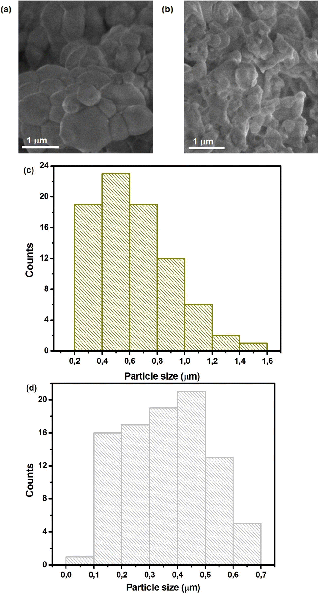 | ||
| Fig. 3 A comparative look at the morphology of A3Bi2I9 (A = Cs, Rb): (a) and (b) SEM images and (c) and (d) particle size analysis. | ||
To assess the thermal stability of A3Bi2I9 (A = Cs, Rb), we conducted TGA measurements, as depicted in Fig. 4. Initially, we noted a slight decrease in weight around 315 and 265 °C for Cs3Bi2I9 and Rb3Bi2I9, respectively. This decrease can be attributed to the breakdown of organic capping ligands.24 Subsequently, a secondary weight reduction commenced around 485 and 445 °C for Cs3Bi2I9 and Rb3Bi2I9, respectively. This decline signifies the onset of A3Bi2I9 decomposition into AI (A = Cs, Rb) and BiI3.24
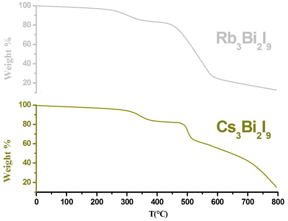 | ||
| Fig. 4 Investigating thermal stability of A3Bi2I9 (A = Cs, Rb): a thermogravimetric analysis (0–800 °C). | ||
Fig. 5(a) and (b) present the UV-Vis absorption spectra of A3Bi2I9 (A = Cs, Rb) measured across a wavelength range of 300 nm to 800 nm. For a more detailed analysis, the Tauc method28–30 was applied to the absorption spectrum obtained from a single crystal of A3Bi2I9 (A = Cs, Rb) (the insets of Fig. 5(a) and (b)). This analysis revealed a direct bandgap (Eg) value of 2.03 eV for Cs3Bi2I9 and 1.90 eV for Rb3Bi2I9.
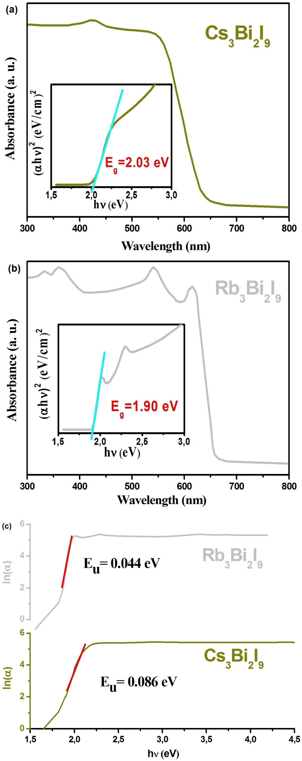 | ||
| Fig. 5 Optical band gap of (a) Cs3Bi2I9 and (b) Rb3Bi2I9 single crystals: a combined approach utilizing room-temperature absorption measurements, Tauc plot and (c) Urbach analysis. | ||
The Urbach energy (EU), symbolized by EU, is a material property associated with the exponential tail observed in absorption spectra at the band edge. This tail arises from electronic transitions between extended states in the valence band and localized states within the conduction band.29 The Urbach energy is an empirically derived parameter that provides valuable information about the defect density within a material.31 Urbach's law establishes an empirical relationship between the absorption coefficient (α) and photon energy (hν) as expressed in eqn (S1).† This equation allows researchers to estimate the degree of structural disorder within a material by analyzing the slope of the linear portion of the α vs. ln(hν) plot derived from the absorption spectrum. Analysis of the absorption spectra using Urbach's law yielded Urbach energy (EU) values of 0.086 eV and 0.044 eV for Cs3Bi2I9 and Rb3Bi2I9, respectively.
Raman spectroscopy was employed to investigate the vibrational modes of A3Bi2I9 (A = Cs, Rb) single crystals at room temperature using a 785 nm laser excitation source (Fig. 6). The Raman spectra of both Cs3Bi2I9 and Rb3Bi2I9 were acquired across a wavenumber range of 2000 cm−1. Interestingly, no significant Raman peaks were detected above 200 cm−1 for either material. The Raman spectra of Rb3Bi2I9 and Cs3Bi2I9 reveal distinct vibrational modes. Rb3Bi2I9 exhibits two prominent peaks located above 125 cm−1. Additionally, several overlapping peaks are observed below 75 cm−1. However, Cs3Bi2I9 shows a distinctive feature – many strong vibrational modes present between 120 and 80 cm−1 that are absent in Rb3Bi2I9. The observed disparity in the Raman spectra can be attributed to the distinct crystal structures of Cs3Bi2I9 and Rb3Bi2I9. Cs3Bi2I9 adopts a molecular salt structure, featuring discrete [Bi2I9]3− anions. These complex anions allow for additional vibrational modes involving Bi–I bonds, leading to the presence of several strong peaks between 120 and 80 cm−1 that are absent in Rb3Bi2I9. In contrast, Rb3Bi2I9 possesses a more uniform structure with BiI6 octahedra, resulting in the two prominent peaks observed above 125 cm−1 for this material. Table S1† summarizes the prominent peaks of A3Bi2I9 (A = Cs, Rb). A closer examination of the vibrational modes observed in the Raman spectrum of Cs3Bi2I9 (space group P63/mmc) suggests their primary source lies within the [Bi2I9]3− anion.32 The crystal structure of Cs3Bi2I9 plays a crucial role in understanding the observed Raman peaks. This structure features discrete, covalently bonded [Bi2I9]3− anions. Each anion is surrounded by and electrostatically bound to three Cs+ cations. This arrangement leads to two distinct types of vibrational modes:
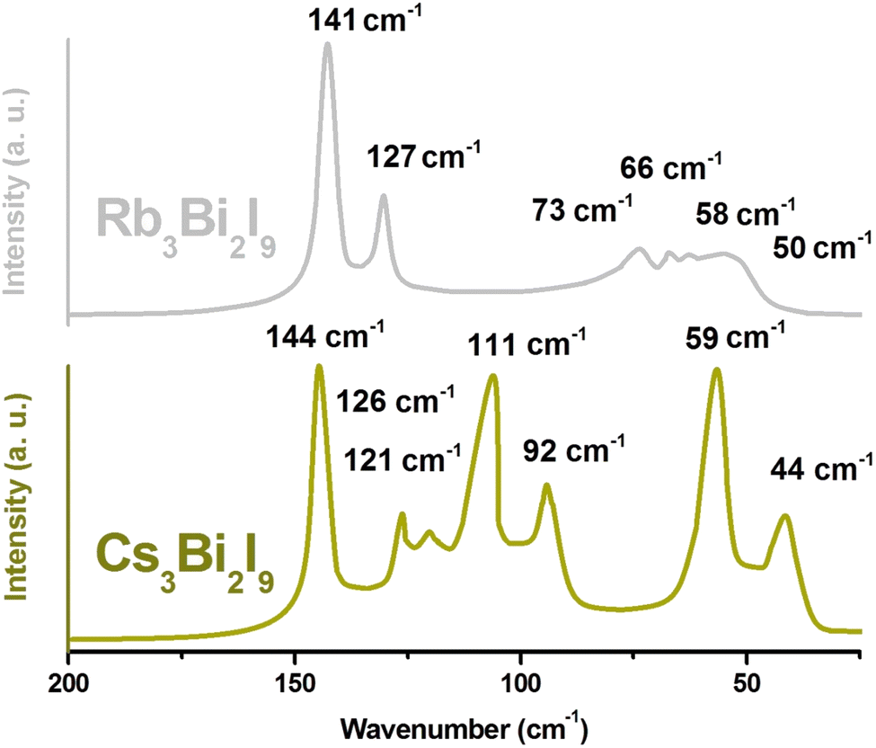 | ||
| Fig. 6 Comparative analysis of A3Bi2I9 perovskites (A = Cs, Rb) by room-temperature Raman spectroscopy (785 nm excitation). | ||
• Dominant vibrations: These originate from within the strongly bound [Bi2I9]3− units due to the covalent Bi–I bonds. These are expected to be the most prominent peaks in the Raman spectrum.
• Weaker modes: These arise from the weaker ionic interactions between the [Bi2I9]3− anions and the bridging Cs+ cations. These modes are likely to be less intense compared to the dominant vibrations.
The dominant vibrational modes observed in the Raman spectrum of Cs3Bi2I9 are expected to originate from within the [Bi2I9]3− anion itself. These modes primarily involve stretching vibrations of the Bi–I bonds. There are two key types of Bi–I bonds within the anion:
• Terminal Bi–I stretching: These involve the six iodine atoms located at the periphery of the [Bi2I9]3− unit.
• Bridging Bi–I stretching: These involve the three iodine atoms that bridge the two central bismuth atoms within the anion, linking them together. The stretching vibrations of both terminal and bridging Bi–I bonds are expected to contribute significantly to the observed Raman peaks for Cs3Bi2I9.
Following the established Nakamoto notation for vibrational modes,33 the Raman spectrum of Cs3Bi2I9 is expected to exhibit specific peaks corresponding to stretching vibrations within the [Bi2I9]3− anion.34 Each set of Bi–I bonds (terminal and bridging) can potentially give rise to three Raman-active stretching modes:
• A′1 symmetric stretch: This mode involves the simultaneous contraction and expansion of both bonds in a symmetrical manner.
• E′′ antisymmetric stretch (1): This mode involves the bonds stretching out of phase with each other (one contracts while the other expands).
• E′ antisymmetric stretch (2): This mode represents another type of out-of-phase stretching motion, potentially different from the first E′′ mode.
Therefore, considering both terminal and bridging Bi–I bonds within the [Bi2I9]3− anion, a total of six distincts stretchings modes could be observed in the Raman spectrum. The observed Raman spectrum of Cs3Bi2I9 likely reveals a correlation between the bond strength and the energy (and therefore, position) of the corresponding Raman peaks for Bi–I stretching modes. This can be explained by the differences in the Bi–I bonding environment within the [Bi2I9]3− anion. Terminal Bi–I bonds involve iodine atoms located at the periphery of the anion and participate in only one Bi–I bond. In contrast, bridging Bi–I bonds involve iodine atoms that connect the two central bismuth atoms and participate in bonds with both Bi atoms. As a result, terminal Bi–I bonds are expected to be stronger due to the absence of bond sharing. Since the energy of a vibrational mode is often related to the strength of the involved bonds, the Raman peaks corresponding to the higher energy stretching modes in the spectrum are likely attributed to the stronger terminal Bi–I bonds. The prominent peak observed at 144 cm−1 is assigned to the most likely candidate – the symmetric terminal Bi–I stretch denoted as A′1 (v1). Its antisymmetric counterparts, the E′′ (v15) and E′ (v10) modes, are tentatively assigned to the peaks at 126 and 121 cm−1, respectively. However, it is important to acknowledge that further investigations might be necessary to confirm these assignments definitively. The Raman spectrum of Cs3Bi2I9 reveals a distinct peak at 111 cm−1 which can be tentatively assigned to the symmetric stretching mode of the bridging Bi–I bonds within the [Bi2I9]3− anion. This mode corresponds to the A′1 (v2) notation in the Nakamoto convention.33 Its antisymmetric counterpart, the E′′ (v7) mode, is likely responsible for the peak observed at 92 cm−1. These assigned peak positions are consistent with values reported in previous studies.35,36 Interestingly, the spectrum appears to lack a distinct peak corresponding to the E′ (v11) mode, which is expected for the antisymmetric stretching of bridging Bi–I bonds. However, the observed width of the E′′ (v7) peak is broader compared to the E′′ and E′ peaks assigned to terminal Bi–I bonds. This broader width might suggest the possible overlap of the E′′ (v7) peak with a weaker E′ (v11) peak, which could be obscured within the broader signal. The broad Raman peaks in both spectra can be attributed to overlapping vibrational modes and potential structural disorder within the crystals. The Raman spectrum of Cs3Bi2I9 exhibits lower energy peaks compared to the stretching modes discussed previously. These lower energy peaks likely correspond to various bending vibrations of the bonds within the [Bi2I9]3− anion, as well as weaker vibrational modes arising from the interaction between these anions and the surrounding Cs+ cations. However, due to the complexity of these modes, assigning them to specific bonds or interactions definitively requires additional techniques like polarization experiments and theoretical calculations. One interesting observation is the unusually strong peak centered at 58 cm−1 compared to the higher energy stretching modes. This can be attributed to the unique crystal structure of Cs3Bi2I9, classified as a molecular salt. In this structure, the [Bi2I9]3− anions are not rigidly bound in specific orientations by the Cs+ cations. This allows the anions a certain degree of rotational and twisting freedom within the lattice. This freedom of movement within the lattice enables the bending modes of the Bi–I bonds to occur as frequently as the stretching modes. This behavior contrasts sharply with compounds that possess a covalently bonded network, where such bending motions are restricted. The observed strong peak at 58 cm−1 is likely a consequence of these bending modes. Additionally, the rotational symmetry of the [Bi2I9]3− anion and the strong Bi–I coupling within it contribute to the situation where the rotational bending of iodine atoms around the central Bi–Bi axis becomes energetically similar to the symmetric stretching motions.
The Raman spectrum of Rb3Bi2I9 presents a distinct contrast compared to Cs3Bi2I9. Unlike the broader range of vibrational modes observed in Cs3Bi2I9, Rb3Bi2I9 exhibits a simpler spectrum. This difference can be attributed to the varying crystal structures of these materials. The key feature of the Rb3Bi2I9 spectrum is the presence of two dominant peaks positioned above 125 cm−1. These peaks likely correspond to the same Bi–I stretching modes observed in Cs3Bi2I9, but with slightly lower wavenumbers. Based on the Nakamoto notation, the higher energy peak at 141 cm−1 can be tentatively assigned to the symmetric A1g (v1) Bi–I stretching mode. The lower energy peak at 127 cm−1 is then likely its counterpart, the Eg (v2) antisymmetric Bi–I stretching mode.33
The Rb3Bi2I9 Raman spectrum also exhibits several overlapping peaks at lower wavenumbers compared to the dominant high-energy features. These lower energy peaks are likely a consequence of various bending vibrations within the molecule. Due to the complex nature of these bending modes, assigning them to specific bonds definitively requires further investigation. The relatively low intensity of these bending modes can be attributed to the constraints imposed by the covalent network in Rb3Bi2I9. This behavior is similar to what is observed in Cs3Bi2I9, where the covalently bonded BiI6 octahedra restricts the bending motions of the bonds.18
In examining the electrical characteristics of A3Bi2I9 (A = Cs, Rb), we conducted an analysis of SCLC on the Au/A3Bi2I9/Au device, as depicted in Fig. 7. This analysis was carried out based on eqn (S2).† Consequently, the determined trap density (ntrap) for Cs3Bi2I9 stands at 7.76 × 109 cm−3, exhibiting a lower value compared to Rb3Bi2I9, which registers at 3.98 × 1010 cm−3. This suggests Cs3Bi2I9 exhibits comparatively fewer charge trapping defects than Rb3Bi2I9, indicating potentially superior electrical properties.37
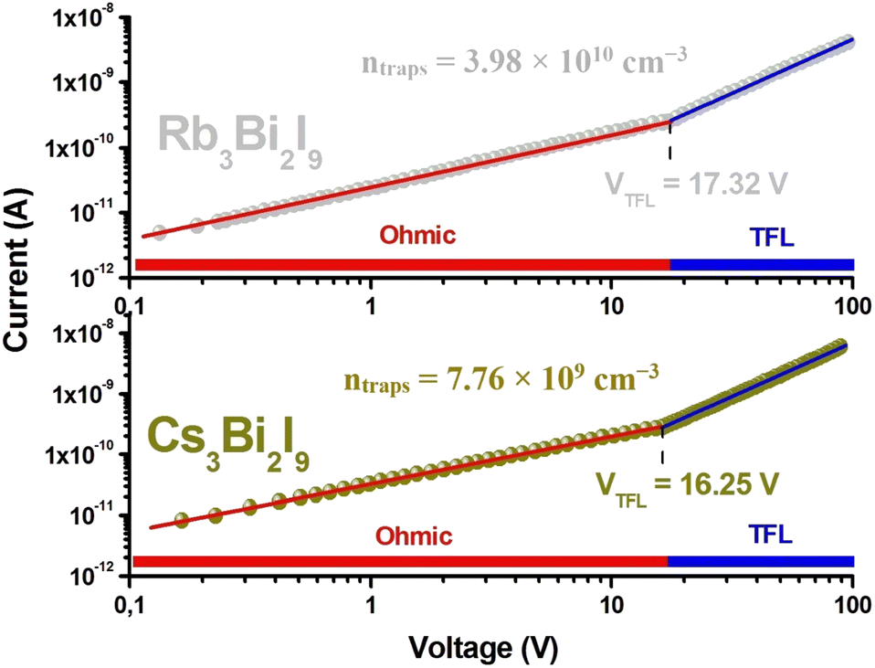 | ||
| Fig. 7 Electrical characterization of A3Bi2I9 (A = Cs, Rb) perovskites at room temperature: unveiling current–voltage behavior. | ||
Complex impedance spectroscopy (CIS) emerged as a valuable tool for characterizing the electrical behavior of A3Bi2I9 (A = Cs, Rb). This technique allows for the simultaneous investigation of two key electrical properties: ion mobility and electrical conductivity. By analyzing the impedance response of the material, CIS provides insights into both the movement of ions within the lattice and the overall ability of the material to conduct electricity.38–40 CIS stands out as a powerful, non-destructive technique for probing the electrical properties of materials. Unlike other methods, CIS avoids sample damage while offering crucial insights into key parameters like electrical conductivity, relaxation time, and ion mobility within A3Bi2I9 perovskites. Furthermore, CIS possesses a unique capability – the ability to differentiate contributions from various sources within the material. By employing a time-reversed electric field, CIS can separate the electrical response of the bulk material, grain boundaries, and electrodes.38–40 This ability to deconvolute contributions provides a much more comprehensive understanding of the electrical behavior within A3Bi2I9. In CIS, the application of an alternating electric field plays a crucial role in investigating charge transport within A3Bi2I9 (A = Cs, Rb). This alternating field interacts with the material, activating charge carriers (ions and electrons). This activation leads to a series of events:
• Formation of space charge: The movement of charges creates a localized region of excess or deficit charge within the material.
• Charge displacement: The alternating field induces the movement of these charges, contributing to the overall current flow.
• Dipole orientation: The field can also influence the orientation of polar molecules or defect dipoles present within the material.
These combined effects allow CIS to distinguish the contributions of various components to the overall impedance of the material. By analyzing the frequency dependence of the measured impedance (as described by eqn (S3)†), it becomes possible to differentiate the contributions of electrodes, grain boundaries, and the bulk material (grains) to the transport of charge carriers within A3Bi2I9.
The electrical properties of A3Bi2I9 (A = Cs, Rb) exhibit a temperature dependence, as revealed by the analysis of the real part (Z′) of the complex impedance (Fig. 8(a)). Notably, increasing temperature and frequency both lead to a decrease in Z′. This observed trend suggests a negative temperature coefficient of resistance (NTCR) behavior in these materials.41 The observed decrease in Z′ with increasing temperature and frequency suggests two potential mechanisms influencing the electrical behavior of A3Bi2I9 (A = Cs, Rb):
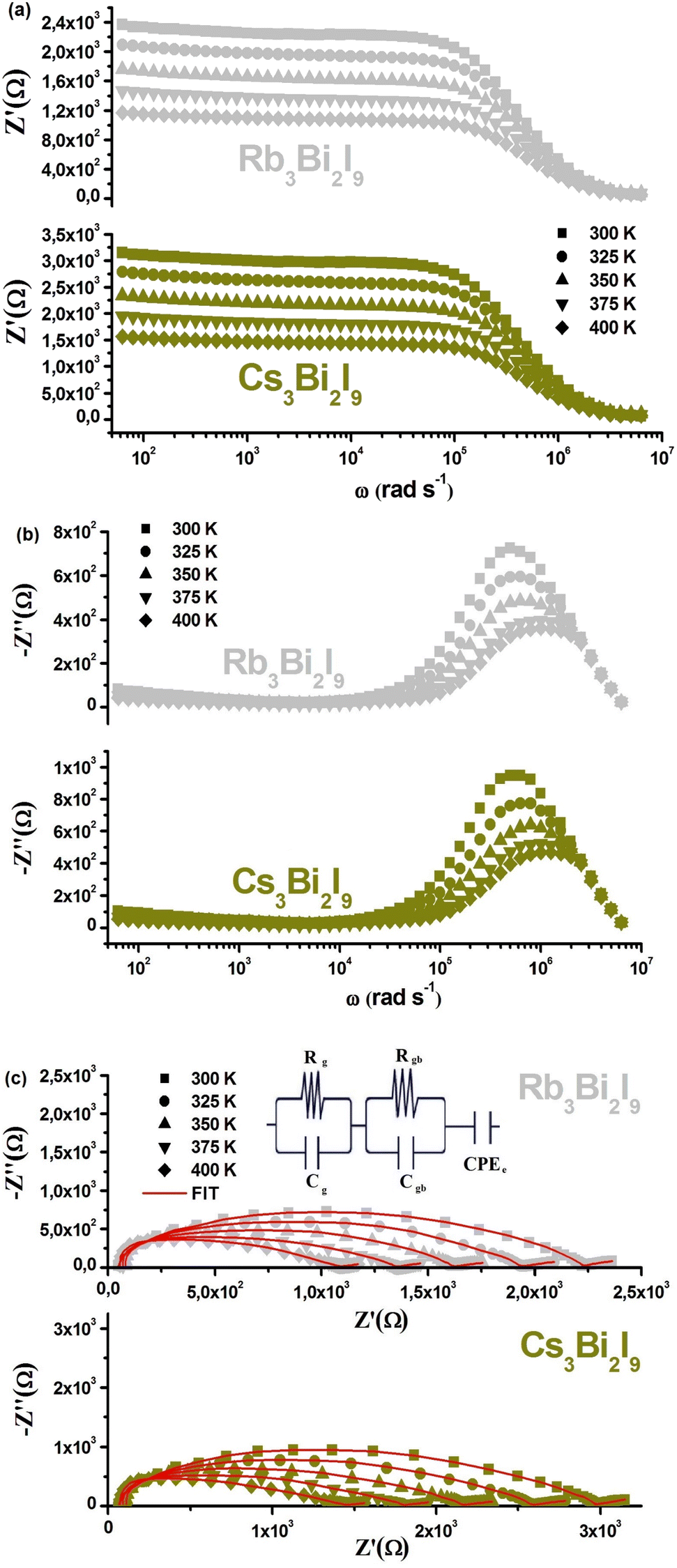 | ||
| Fig. 8 Deciphering the impedance behavior of A3Bi2I9 perovskites (A = Cs, Rb): (a)–(c) a combined approach using frequency and temperature dependence with equivalent circuit modeling. | ||
• Enhanced AC conductivity: The decrease in Z′ can be attributed to an increase in the alternating current (AC) conductivity within the material. This could be due to a reduction in the density of trapped charges. As temperature rises, trapped charges may gain enough energy to escape their localized positions and contribute to overall conductivity. Additionally, increased frequency can limit the time available for charges to become trapped, further enhancing conductivity.39–41
• Space charge influence: At high frequencies, the observed temperature-independent behavior of Z′ points towards the presence of space charge within the material for both Cs3Bi2I9 and Rb3Bi2I9. Space charge refers to a localized region of excess or deficit charge within the material. At high frequencies, the rapid fluctuations of the alternating field may not effectively penetrate the entire material, resulting in a dominant contribution from the space charge layer to the impedance, leading to a less pronounced temperature dependence of Z′.39–41
The variations in the loss factor (Z′′) depicted in Fig. 8(b) for A3Bi2I9 (A = Cs, Rb) across different frequencies and temperatures offer valuable insights into the relaxation processes and dominant charge transport mechanisms within these materials. The observed changes in Z′′ can be attributed to the relaxation of mobile charges after an applied electric field is removed. At higher temperatures, the relaxation process is likely dominated by the movement of defects or vacancies within the crystal structure. These defects or vacancies can act as temporary traps for charge carriers, hindering their movement. However, at higher temperatures, these trapped charges gain enough energy to overcome the trapping potential and contribute to the overall conductivity. This results in a more efficient relaxation process, reflected by a lower peak in Z′′ at higher temperatures.42 Conversely, at lower temperatures, the relaxation process is expected to be governed by the movement of immobile species or electrons. These species or electrons may be tightly bound within the crystal lattice or possess limited mobility due to the lower thermal energy. Consequently, the relaxation process becomes sluggish, leading to a broader and potentially higher peak in Z′′ observed at lower temperatures. Analysis of the loss factor (Z′′) spectra for A3Bi2I9 (A = Cs, Rb) (as shown in Fig. 8(b)) reveals the presence of a distinct peak, often referred to as the “relaxation frequency.” This peak signifies a characteristic frequency at which the relaxation process of mobile charges within the material becomes most prominent.39 Notably, the broadness of the peak observed in these materials suggests a deviation from the ideal Debye relaxation model, which assumes a single, well-defined relaxation time for all charge carriers. The spectra offer insights into the dominant modes of charge transport across different frequency ranges. Below the relaxation peak frequency, the movement of charge carriers is likely dominated by a long-range transport mechanism. This could involve the migration of charges across relatively large distances within the crystal lattice.41 In contrast, at frequencies exceeding the relaxation peak frequency, the spectra suggest a shift towards the movement of more localized charge carriers. These localized carriers may be temporarily trapped within the lattice or possess limited mobility due to interactions with defects or other localized states. As temperature increases, the relaxation peak exhibits a distinct shift towards higher frequencies. This observation suggests a thermally activated relaxation process within the material.39,40 In simpler terms, the relaxation of mobile charges within the crystal lattice becomes faster at elevated temperatures. This could be attributed to factors like increased thermal energy, allowing charge carriers to overcome potential barriers or defects more efficiently. Interestingly, the peak height also exhibits a temperature dependence, decreasing with increasing temperature. This trend points towards a decline in the overall resistance experienced by the charge carriers. This potentially indicates a decrease in both grain boundary resistance and resistance within the bulk grains (grains) of the material. As temperature rises, the mobility of charge carriers might improve, leading to a reduction in the resistance encountered at these interfaces and throughout the material. This aligns with observations reported in previous studies.38–41
The Cole–Cole plots presented in Fig. 8(c) for A3Bi2I9 (A = Cs, Rb) offer valuable insights into the electrical relaxation processes within the materials across a temperature range of 300 to 400 K. Notably, both materials exhibit depressed semicircles instead of perfect semicircles in the Cole–Cole plots. This deviation from the ideal Debye model indicates the presence of non-Debye relaxation behavior. In simpler terms, the relaxation of mobile charges within the material does not occur with a single, well-defined relaxation time but rather involves a distribution of relaxation times. Furthermore, the Cole–Cole plots display a trend where the radii of the semicircles decrease with increasing temperature. This observation aligns with the negative temperature coefficient of resistance (NTCR) behavior observed in these materials. As temperature rises, the overall resistance to charge transport within the material decreases, which is reflected by the shrinking radii of the semicircles in the Cole–Cole plots. This finding aligns with previous reports on NTCR behavior in similar materials.43 The electrical properties of A3Bi2I9 (A = Cs, Rb), as revealed by the Nyquist plots (Fig. 8(c)), suggest characteristics typical of semiconductors. This implies that the dominant conduction mechanism within these materials is thermally activated. In simpler terms, the conductivity increases with rising temperature as more charge carriers gain enough thermal energy to participate in conduction processes. The ideal Nyquist plot for this type of material would typically showcase three distinct semicircles. Each semicircle represents the impedance contribution from a specific region within the material:43
• High-frequency semicircle: This semicircle observed at higher frequencies corresponds to the contribution of the bulk material (grains). It reflects the intrinsic resistance and capacitance associated with the movement of charge carriers within the crystal lattice.
• Low-frequency semicircle: The semicircle observed at lower frequencies represents the contribution of the grain boundaries. Grain boundaries can act as regions of higher resistance compared to bulk material due to defects or limited mobility of charge carriers at these interfaces.
However, interpreting the contributions from different regions of the material can be challenging. While the presence of a single, depressed semicircle often reflects the combined influence of grains and grain boundaries due to their overlapping frequency ranges, the Nyquist plot can also reveal a separate contribution from the electrode–material interface at ultra-low frequencies. This contribution from the electrode–material interface arises due to interfacial phenomena such as charge transfer processes or the formation of a double electric layer at the contact points between the electrodes and the material. It typically manifests as a smaller semicircle at very low frequencies in the Nyquist plot. To fully disentangle the contributions from these various regions, researchers often employ the Maxwell–Wagner equivalent circuit model.40 This model represents the electrical behavior using a parallel combination of resistors (R) and capacitors (C), where each element corresponds to a specific region or process: even when they appear as a combined response in the Nyquist plot. This approach provides a more comprehensive understanding of the electrical properties within the material. To gain a deeper understanding of the electrical behavior of A3Bi2I9 (A = Cs, Rb), an equivalent circuit model has been employed. This model, fitted using ZView software for the impedance spectra across various temperatures, consisted of two parallel RC (resistor–capacitor) elements connected in series. Each element represents the electrical properties of a specific region within the material:
• Bulk material (grains): Represented by the first RC element, it reflects the intrinsic resistance (Rg) to charge transport and the associated capacitance (Cg) within the crystal lattice.
• Grain boundaries: Modeled by the second RC element (Rgb, Cgb), it accounts for the higher resistance encountered at grain boundaries due to factors like defects or limited charge carrier mobility.
The Nyquist plots (refer to Fig. 8(c)) also reveal a straight line following the semicircle at lower frequencies. This behavior is attributed to the presence of a constant phase element (CPE), which often arises due to inhomogeneities in the electrode surface and the formation of a double-layer capacitance. The inset figures provide a closer look at this low-frequency region. A significant observation from the Nyquist plots is the decrease in the diameter of the semicircle and its intersection with the real axis as temperature increases. This trend suggests an enhancement in the DC conductivity of A3Bi2I9 (A = Cs, Rb) at higher temperatures.39 Furthermore, analysis of the fitted parameters (Table S2†) reveals that the resistance associated with grain boundaries (Rgb) consistently exceeds the resistance within the grains (Rg) across all temperatures. This difference in resistance values contributes to the accumulation of space charges at the grain boundaries due to a phenomenon known as the Maxwell–Wagner effect.40 As mentioned previously,39 grain boundaries are generally more resistive than the bulk material (grains) in perovskite materials.38
Fig. 9(a) depicts the fascinating interplay between temperature and frequency on the AC conductivity of A3Bi2I9 (A = Cs, Rb) crystals. The AC conductivity, calculated using eqn (S4),† dominates the overall conductivity at high frequencies. In contrast, the low-frequency range reflects the temperature-dependent and frequency-independent DC conductivity. This explains the plateau observed in the curves at lower frequencies.44 As frequency increases, the AC conductivity contributions become significant, leading to a pronounced rise and frequency dispersion (dependence on frequency) in the conductivity curves. This transition from DC to AC-dominated behavior occurs at a specific frequency, often referred to as the “hopping frequency.” Notably, the hopping frequency (represented by a symbol, which can be removed) shifts towards higher frequencies with increasing temperature. Funke's jump relaxation model (JRM) offers a compelling explanation for the observed trends.45 At low frequencies, the model suggests that ions within the material can successfully hop to neighboring sites. These successful hops contribute to long-range, translational motion of the ions, ultimately leading to a sustained DC conductivity observed at low frequencies. However, at higher frequencies, the hopping process becomes more dynamic. According to the JRM, these hops can either be successful (resulting in ion movement and conductivity) or unsuccessful (where the ion returns to its original position and doesn't contribute to conductivity). This interplay between successful and unsuccessful hops at high frequencies explains the frequency dispersion observed in the AC conductivity.45
 | ||
| Fig. 9 (a) Unveiling the temperature–frequency landscape of AC conductivity in A3Bi2I9 (A = Cs, Rb). (b) Extracting activation energy for electrical conduction using an Arrhenius-like approach. (c) Unveiling the temperature dependence of charge transport mechanisms in A3Bi2I9 (A = Cs, Rb). (d) Investigating charge transport dynamics in A3Bi2I9 (A = Cs, Rb): unveiling the role of relaxation processes through Rω analysis. (e) Frequency-dependent of Rω. | ||
The JRM model provides a framework for understanding the observed frequency dependence of AC conductivity. According to this model, the hopping behavior of ions within the material plays a crucial role. At low frequencies, the hopping process is dominated by successful events. Here, an “excited” ion successfully jumps to a neighboring site, contributing to long-range translational motion within the material. These successful hops ultimately lead to the sustained DC conductivity observed at lower frequencies. However, as the frequency increases, the hopping dynamics become more complex. JRM suggests that hops can now be both successful and unsuccessful. In an unsuccessful hop, the excited ion may oscillate back and forth before returning to its initial position. This unsuccessful hopping doesn't contribute to the overall movement of ions and therefore doesn't contribute to conductivity. With increasing frequency, the proportion of unsuccessful hops increases compared to successful ones. This imbalance leads to the observed dispersion in the conductivity curves at high frequencies (dispersive conductivity). The measured electrical conductivity can be described by Jonscher's power law (eqn (S5)†), which mathematically captures this frequency dependence.45
The experimental data for AC conductivity variation (σAC(ω)) presented in Fig. 9(a) was employed to determine the DC conductivity (σDC) values for A3Bi2I9 (A = Cs, Rb) across all investigated temperatures. This analysis utilized the Universal Dielectric Response (UDR) approach. Following the UDR analysis, Fig. 9(b) depicts a plot of the natural logarithm of DC conductivity (ln(σDC)) versus the inverse of temperature (1000/T). This plot allows for the calculation of the average activation energies for both materials using the Arrhenius equation (eqn (S6)†). The Arrhenius equation relates the temperature dependence of conductivity to the activation energy, a parameter that reflects the energy barrier for charge carriers to participate in conduction processes. The activation energy values for Cs3Bi2I9 and Rb3Bi2I9 stand at 0.155 eV and 0.135 eV, respectively.
Understanding the charge transport mechanisms within A3Bi2I9 (A = Cs, Rb) crystals is crucial. By analyzing the temperature dependence of the exponent ‘s’ (refer to Fig. 9(c)), researchers can gain valuable insights into the dominant processes. Several theoretical models have been proposed in the literature to explain the behavior of ‘s’.38–41 These models often involve a combination of quantum mechanical tunneling and/or hopping of charge carriers (electrons/polarons or even atoms) across potential barriers. Some prominent examples include overlapping large polaron tunneling (OLPT), non-overlapping small-polaron tunneling (NSPT), correlated barrier hopping (CBH), and pure quantum mechanical tunneling (QMT). Insights from ‘s’ for Cs3Bi2I9 and Rb3Bi2I9:
• Cs3Bi2I9: The observed decrease in ‘s’ with increasing temperature, followed by a slight increase, suggests that the OLPT model might be most suitable for Cs3Bi2I9. This behavior aligns with the characteristics of overlapping large polarons, where the tunneling probability increases at lower temperatures due to a larger overlap between adjacent polarons.
• Rb3Bi2I9: In contrast, Rb3Bi2I9 exhibits an increase in ‘s’ with temperature. This trend points towards the NSPT model as a better fit. NSPT describes the hopping of smaller polarons with minimal overlap between them. As temperature rises, the thermal energy likely aids these hops, leading to a higher value of ‘s’.
For a deeper understanding of the fitting process, detailed descriptions of the OLPT and NSPT models are provided in the ESI.† Fig. 9(d) presents a crucial piece of evidence supporting the chosen models. It depicts the variation of the natural logarithm of AC conductivity (ln(σAC)) with temperature for both A3Bi2I9 (A = Cs, Rb) materials. The key takeaway from this figure is the excellent agreement between the fitting curves based on the OLPT and NSPT models and the actual experimental data points. This agreement strengthens the validity of our model selection. This fitting process served another important purpose: extracting the key parameters associated with both the OLPT and NSPT models. These extracted parameters hold valuable information about the charge transport mechanisms within the materials. Tables S3–S5† present the complete set of parameters obtained for Cs3Bi2I9 and Rb3Bi2I9.
The analysis of the extracted parameters for Cs3Bi2I9 provides compelling evidence supporting the selection of the overlapping large polaron tunneling (OLPT) model. Notably, the value of the parameter α falls within the range reported by Murawski et al.46 for similar systems involving localized states, which aligns with the characteristics of large polarons in the OLPT model. Fig. 9(e) further strengthens this connection. It depicts the frequency dependence of the parameter Rω for Cs3Bi2I9. Interestingly, the calculated tunneling distances (Rω) range from 4.212 to 4.302 Å. This range is remarkably close to the interatomic distances between Cs and I ions (Cs–I) within the Cs3Bi2I9 crystal lattice, which is reported to be between 4.204 and 4.318 Å.47 This close correspondence between the tunneling distances and interatomic spacings suggests that the mobility of Cs+ cations might play a crucial role in facilitating AC conductivity. The large polarons associated with the OLPT model can leverage the movement of these cations to enhance conductivity through the material.
Similar to Cs3Bi2I9, the extracted parameters for Rb3Bi2I9 provide valuable insights into the chosen model (NSPT). The observed values for the relevant parameters fall within the expected range for localized states, consistent with the characteristics of small polarons in the NSPT model.38 Table S5† depicts the frequency dependence of two key parameters, N(EF) and α, for Rb3Bi2I9. Interestingly, both parameters exhibit a decreasing trend with increasing frequency. This observed behavior aligns well with previous reports on similar systems.39 Fig. 9(e) sheds further light on the hopping behavior within Rb3Bi2I9. It displays the frequency dependence of Rω, revealing a decrease in the hopping distance as frequency increases. This trend suggests a shift from long-distance to short-distance tunneling by the charge carriers at higher frequencies. This shift might be linked to the observed increase in N(EF) (carrier density) with frequency, as reported elsewhere.39 Another noteworthy observation is the close match between the calculated tunneling distances (Rω, ranging from 3.312 to 4.214 Å) and the interatomic distances between Rb and I ions (Rb–I) within the Rb3Bi2I9 crystal lattice (reported to be between 3.273 and 4.224 Å).48 This similarity suggests that the mobility of Rb+ cations might play a significant role. The NSPT model proposes that small polaron motion can leverage the movement of these cations to facilitate AC conductivity within the material.
In this section, we aim to compare the optical and electrical properties of the compounds A3Bi2I9 (A = Cs, Rb). The structural disparity between Cs3Bi2I9 and Rb3Bi2I9, with Cs3Bi2I9 adopting a 0D molecular salt crystal structure and Rb3Bi2I9 featuring 2D layered derivatives of the perovskite structure, likely influences their optical properties. Cs3Bi2I9's hexagonal symmetry and disparate [Bi2I9]3− anions might lead to a wider bandgap (Eg) of 2.03 eV compared to Rb3Bi2I9's 1.90 eV, suggesting stronger electronic confinement. Moreover, the higher Urbach energy in Cs3Bi2I9 (0.086 eV) compared to Rb3Bi2I9 (0.044 eV) may signify a broader distribution of localized states, possibly due to its more complex crystal structure, impacting its optical absorption properties. Fig. 10 presents a combined analysis of the electrical conductivity behavior in A3Bi2I9 (A = Cs, Rb) at room temperature (300 K). This analysis includes both Nyquist plots and the frequency dependence of AC conductivity (σAC). A key takeaway from this figure is the noticeably larger conductivity observed in Rb3Bi2I9 compared to Cs3Bi2I9. The specific features of the Nyquist plots and the trend in the σAC curves with frequency both support this conclusion. The observed higher conductivity in Rb3Bi2I9 compared to Cs3Bi2I9 may be attributed to the mass difference of the A+ cation (Cs = 132.9 u/Rb = 85.4 u). With Rb having a smaller mass relative to Cs, it suggests that the delocalization of the A cation in Rb3Bi2I9 is more facile compared to Cs3Bi2I9. This facilitates easier movement of charge carriers, leading to enhanced AC conductivity, as evidenced by the decrease in hopping distances with increasing frequency in Rb3Bi2I9. The proximity of the tunneling distances to the interatomic distances within the crystal lattice further supports this interpretation, indicating efficient charge transport facilitated by small polaron motion in Rb3Bi2I9. In addition to the mass difference of the A+ cation, the disparity in crystal structure between Cs3Bi2I9 (0D) and Rb3Bi2I9 (2D) likely contributes to the variation in conductivity. The 0D molecular salt crystal structure of Cs3Bi2I9, with its hexagonal symmetry and disparate [Bi2I9]3− anions, may restrict charge carrier mobility compared to the 2D layered derivatives of the perovskite structure in Rb3Bi2I9. The 2D layered structure of Rb3Bi2I9 facilitates charge transport along the layers, potentially leading to enhanced AC conductivity due to reduced hindrance for charge carriers compared to the more constrained 0D structure of Cs3Bi2I9.
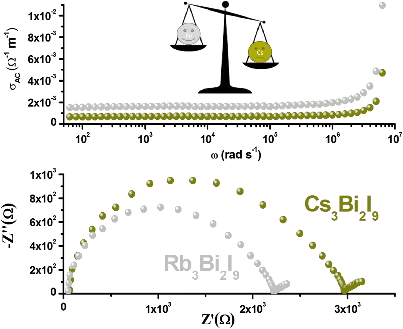 | ||
| Fig. 10 Unveiling electrical properties of A3Bi2I9 (A = Cs, Rb) perovskites: a combined approach using Nyquist plots and AC conductivity (300 K). | ||
To further investigate the conduction mechanism and gain insights into the nature of polarons within A3Bi2I9 (A = Cs, Rb), transient absorption spectroscopy was employed. This technique involved exciting the samples with a laser pulse centered at a wavelength of 350 nm and monitoring the resulting changes in light absorption over time. By analyzing these transient absorption signals, researchers aimed to elucidate the dominant charge transport mechanisms and characterize the properties of the polarons, which are quasiparticles that influence conductivity in these materials.
Fig. 11(a) and (b) display the measured absorption spectrum after light excitation. A prominent photoinduced absorption (PIA) band is observed within the 400–700 nm wavelength range. This broad band signifies the formation of self-trapped states (STS) just below the material's band edge. The presence of a broad PIA band aligns with established observations during STS formation in other materials.49,50
 | ||
| Fig. 11 (a) and (b) Femtosecond-scale transient absorption spectroscopy of A3Bi2I9 (where A = Cs or Rb) following 350 nm optical excitation and probing within the 450–700 nm wavelength range. (c) and (d) Exponential fitting of experimental data indicated by continuous red lines at wavelengths 475 nm and 600 nm. | ||
The intensity of the PIA signal exhibits a rise until around 800 femtoseconds (fs), followed by a rapid decay that reduces the signal significantly within approximately 30 ps. Notably, the entire development of PIA kinetics across the probed wavelength range occurs within a timeframe of roughly 400–800 fs. This rapid rise time suggests the absence of a potential barrier separating free excitons (excited electron–hole pairs) and trapped carriers within the self-trapped states.
To further understand the dynamics of the observed photoinduced absorption (PIA), researchers employed a biexponential decay model. This model assumes the decay can be described by the combined effect of two distinct processes, each characterized by its own time constant. The analysis focused on the data obtained at a wavelength of 475 nm, which coincides with the absorbance band edge of A3Bi2I9 (A = Cs, Rb). The results revealed that the PIA decay could be effectively fitted using two time constants, denoted as τ1 and τ2. Fig. 11(c) and (d) illustrate these findings. For Cs3Bi2I9, the decay was attributed to τ1 with a value of 1.3 ps, accounting for 74.8% of the total decay, and τ2 with a value of 6.7 ps, contributing the remaining 25.2%. Similarly, for Rb3Bi2I9, the decay was described by τ1 (1.7 ps, 71.9%) and τ2 (6.6 ps, 18.1%).
The biexponential decay model analysis was extended to a broader range, encompassing wavelengths from 450 nm to 650 nm. The focus then shifted to the decay kinetics observed at 600 nm, as shown in Fig. 11(c) and (d) for Cs3Bi2I9 and Rb3Bi2I9, respectively. These decay profiles could be effectively described by two time constants, denoted as τ1 and τ2. For Cs3Bi2I9, the values were τ1 = 0.4 ps and τ2 = 4.9 ps, while for Rb3Bi2I9, they were τ1 = 0.2 ps and τ2 = 3.7 ps.
The ultrafast component, τ1, observed at 475 nm (1.3 ps for Cs3Bi2I9 and 1.7 ps for Rb3Bi2I9) is attributed to carrier relaxation via coupling with longitudinal optical (LO) phonons. This phenomenon is associated with the formation of Fröhlich polarons, as documented in previous studies.51,52 Interestingly, the time constant for Fröhlich polaron formation in lead-halide perovskites is typically around 0.2 ps, which closely aligns with the faster time constants observed at 600 nm (τ1 = 0.4 ps and 0.2 ps for Cs3Bi2I9 and Rb3Bi2I9, respectively).
The significant distortion within the soft lattice caused by the Fröhlich polaron can activate various acoustic phonon modes. The interaction between these acoustic phonons and the electrons, along with the ultrafast self-trapping of carriers by these modes, is believed to be responsible for the second decay component observed at both 475 nm and 600 nm. This component is represented by τ2 with values of 6.7 ps and 6.6 ps for Cs3Bi2I9 and Rb3Bi2I9 at 475 nm, respectively, and 4.9 ps and 3.7 ps at 600 nm.
The impedance study and absorption analysis together provide a comprehensive understanding of charge transport and polaron dynamics in A3Bi2I9 (A = Cs, Rb) compounds. The impedance study offers detailed insights into the suitability of different theoretical models and the impact of structural differences on conductivity. Meanwhile, the absorption analysis complements this by revealing the ultrafast dynamics and mechanisms of polaron formation and relaxation. By integrating findings from both analyses, a more complete picture emerges, showing how structural and dynamic properties work together to influence the overall behavior of these materials. This complementarity underscores the importance of using multiple analytical approaches to fully characterize complex material systems.
4. Conclusions
In sum, this study elucidates the influence of monovalent cations on the conduction mechanism in lead-free A3Bi2I9 perovskites (A = Cs, Rb). The synthesis and characterization reveal distinct structural and optical properties between Cs3Bi2I9 and Rb3Bi2I9, with Cs3Bi2I9 exhibiting a wider bandgap and higher Urbach energy due to its 0D molecular salt crystal structure. Raman spectroscopy revealed distinct vibrational modes in Cs3Bi2I9 and Rb3Bi2I9, reflecting their differing crystal structures. Cs3Bi2I9 (molecular salt) exhibited a broader range of peaks compared to Rb3Bi2I9 (octahedral BiI6 units), indicating a more complex vibrational environment within the Cs3Bi2I9 lattice. Furthermore, the observed higher AC conductivity in Rb3Bi2I9 is attributed to the facile delocalization of the smaller mass Rb+ cation, coupled with its 2D layered structure, enabling more efficient charge transport compared to Cs3Bi2I9. This study investigated the carrier dynamics in A3Bi2I9 (A = Cs or Rb) using transient absorption spectroscopy. The results suggest that polarons play a key role in trapping excited charge carriers within the material. Following light excitation, the carriers lose energy through interaction with longitudinal optical (LO) phonons, forming Fröhlich polarons. These polarons further interact with various acoustic phonon modes, leading to their stabilization. The combined effect creates self-trapped states that confine the charge carriers within a limited region of the crystal lattice. This mechanism provides valuable insights into the fundamental processes influencing carrier transport in these materials. These findings underscore the significance of both cation mass and crystal structure in dictating the electrical properties of lead-free perovskite materials, offering insights for their potential applications in optoelectronic devices.Data availability
The data that support the findings of this study are available on request from the corresponding author. The data are not publicly available due to [restrictions e.g. their containing information that could compromise the privacy of research participants].Conflicts of interest
There are no conflicts to declare.Acknowledgements
Dhaifallah R. Almalawi would like to acknowledge Deanship of Scientific Research, Taif University for funding this work.References
- Q. Zhang, D. Zhang, B. Cao, S. Poddar, X. Mo and Z. Fan, ACS Nano, 2024, 18, 8557–8570 CrossRef CAS PubMed.
- I. López-Fernández, D. Valli, C. Wang, S. Samanta, T. Okamoto, Y. Huang, K. Sun, Y. Liu, V. S. Chirvony, A. Patra, J. Zito, L. De Trizio, D. Gaur, H. Sun, Z. Xia, X. Li, H. Zeng, I. Mora-Seró, N. Pradhan, J. P. Martínez-Pastor, P. Müller-Buschbaum, V. Biju, T. Debnath, M. Saliba, E. Debroye, R. L. Z. Hoye, I. Infante, L. Manna and L. Polavarapu, Adv. Funct. Mater., 2024, 34, 2307896 CrossRef.
- S. Znaidia and M. B. Bechir, Opt. Mater., 2023, 145, 114473 CrossRef CAS.
- M. B. Bechir, M. Akermi and H. J. Alathlawi, RSC Adv., 2024, 14, 14221–14232 RSC.
- C. Wang, D. Qu, B. Zhou, C. Shang, X. Zhang, Y. Tu and W. Huang, Small, 2024, 20, 2307645 CrossRef CAS.
- M. B. Bechir and F. Alresheedi, RSC Adv., 2024, 14, 1634–1648 RSC.
- Z. Wang, S. Shu, X. Wei, R. Liang, S. Ke, L. Shu and G. Catalán, Phys. Rev. Lett., 2024, 132, 086902 CrossRef CAS PubMed.
- M. H. Dhaou, M. B. Bechir and S. M. Altrifi, Mater. Res. Bull., 2023, 167, 112381 CrossRef.
- M. B. Bechir and F. Alresheedi, Opt. Mater., 2024, 147, 114621 CrossRef.
- K. Niu, C. Wang, J. Zeng, Z. Wang, Y. Liu, L. Wang, C. Li and Y. Jin, J. Phys. Chem. Lett., 2024, 15, 1006–1018 CrossRef CAS.
- M. B. Bechir and M. Akermi, Opt. Mater., 2024, 152, 115375 CrossRef.
- J. K. Rony, M. Saiduzzaman, M. N. Islam, K. M. Hossain, S. Alam, A. Biswas, M. a. T. Mia, S. Ahmad and S. K. Mitro, J. Mater. Res. Technol., 2024, 29, 897–909 CrossRef CAS.
- V. J. Kumar, A. Kathiravan and M. A. Jhonsi, Nano Energy, 2024, 125, 109523 CrossRef CAS.
- X. Geng, Y. Chen, Y. Li, J. Ren, G. Dun, K. Qin, Z. Lin, J. Peng, H. Tian, Y. Yang, D. Xie and T. Ren, Adv. Sci., 2023, 10, 2300256 CrossRef CAS PubMed.
- B. Wang, X. Yang, R. Li, S. M. H. Qaid, W. Cai, H. Xiao and Z. Zang, ACS Energy Lett., 2023, 8, 4406–4413 CrossRef CAS.
- R. S. Babu, S. Bhandary, D. Chopra and S. P. Singh, Chemistry, 2020, 26, 10519–10527 CrossRef CAS.
- D. Kubicki, D. Prochowicz, A. Hofstetter, S. M. Zakeeruddin, M. Grätzel and L. Emsley, J. Am. Chem. Soc., 2017, 139, 14173–14180 CrossRef CAS PubMed.
- K. M. McCall, C. C. Stoumpos, S. S. Kostina, M. G. Kanatzidis and B. W. Wessels, Chem. Mater., 2017, 29, 4129–4145 CrossRef CAS.
- M. Huma, M. Rashid, Q. Mahmood, E. Algrafy, N. A. Kattan, A. Laref and A. S. Bhatti, Mater. Sci. Semicond. Process., 2021, 121, 105313 CrossRef CAS.
- M. B. Bechir and S. Znaidia, Phys. Chem. Chem. Phys., 2023, 25, 19684–19692 RSC.
- M. B. Bechir, K. Karoui, M. Tabellout, K. Guidara and A. B. Rhaiem, Phase Transitions, 2015, 91, 901–917 CrossRef.
- M. B. Bechir, A. Almeshal and M. H. Dhaou, Mater. Res. Bull., 2023, 157, 112012 CrossRef CAS.
- P. Acharyya, K. Pal, A. Ahad, D. Sarkar, K. S. Rana, M. Dutta, A. Soni, U. V. Waghmare and K. Biswas, Adv. Funct. Mater., 2023, 33, 2304607 CrossRef CAS.
- J. Pal, A. Bhunia, S. Chakraborty, S. Manna, S. Das, A. Dewan, S. Datta and A. Nag, J. Phys. Chem. C, 2018, 122, 10643–10649 CrossRef CAS.
- I. Romdhane, M. B. Bechir and M. H. Dhaou, Phys. E, 2022, 136, 115008 CrossRef CAS.
- M. B. Bechir and M. H. Dhaou, RSC Adv., 2023, 13, 17750–17764 RSC.
- C. Cuhadar, S.-G. Kim, J. Yang, J. H. Seo, D. Lee and N. Park, ACS Appl. Mater. Interfaces, 2018, 10, 29741–29749 CrossRef CAS PubMed.
- R. Kalthoum, M. B. Bechir, A. B. Rhaiem and M. H. Dhaou, Opt. Mater., 2022, 125, 112084 CrossRef CAS.
- R. Kalthoum, M. B. Bechir and A. B. Rhaiem, Phys. E, 2020, 124, 114235 CrossRef CAS.
- S. Znaidia and M. B. Bechir, Ionics, 2023, 30, 1177–1195 CrossRef.
- F. Giustino and H. J. Snaith, ACS Energy Lett., 2016, 1, 1233–1240 CrossRef CAS.
- O. V. Vakulenko, V. O. Gubanov, S. V. Kun, F. V. Motsnyǐ, E. Y. Peresh and V. A. Terekhov, Proc. SPIE-Int. Soc. Opt. Eng., 1998, 3359, DOI:10.1117/12.306241.
- K. Nakamoto, Applications in Inorganic Chemistry, in Infrared and Raman Spectra of Inorganic and Coordination Compounds, John Wiley & Sons, Inc., 2008, pp. 149–354 Search PubMed.
- J. Laane and P. W. Jagodzinski, Inorg. Chem., 1980, 19, 44–49 CrossRef CAS.
- F. V. Motsnyǐ, O. M. Smolanka, V. I. Sugakov and E. Yu. Peresh, Solid State Commun., 2006, 137, 221–224 CrossRef.
- H.-L. Sheu and J. Laane, Inorg. Chem., 2013, 52, 4244–4249 CrossRef CAS PubMed.
- M. B. Bechir and F. Alresheedi, Phys. Chem. Chem. Phys., 2024, 26, 1274–1283 RSC.
- M. B. Bechir and M. Akermi, RSC Adv., 2024, 14, 9228–9242 RSC.
- M. B. Bechir and M. H. Dhaou, Mater. Res. Bull., 2021, 144, 111473 CrossRef CAS.
- M. B. Bechir and M. H. Dhaou, RSC Adv., 2021, 11, 21767–21780 RSC.
- P. Maji, A. Ray, P. Sadhukhan, S. Chatterjee and S. Das, J. Appl. Phys., 2018, 124, 124102 CrossRef.
- P. Maji, S. Chatterjee and S. Das, Ceram. Int., 2019, 45, 6012–6020 CrossRef CAS.
- M. B. Bechir, A. Almeshal and M. H. Dhaou, Ionics, 2022, 28, 5361–5376 CrossRef CAS.
- M. B. Bechir and A. B. Rhaiem, J. Solid State Chem., 2021, 296, 122021 CrossRef.
- S. Pujaru, P. Maji, P. Sadhukhan, A. Ray, B. Ghosh and S. Das, J. Mater. Sci.: Mater. Electron., 2020, 31, 8670–8679 CrossRef CAS.
- L. Murawski, C. H. Chung and J. D. Mackenzie, J. Non-Cryst. Solids, 1979, 32, 91–100 CrossRef CAS.
- A. V. Arakcheeva, M. Bonin, G. Chapuis and A. I. Zaitsev, Z. Kristallogr., 1999, 214, 279–283 CAS.
- V. Sidey, Yu. V. Voroshilov, S. V. Kun and E. Yu. Peresh, J. Alloys Compd., 2000, 296, 53–58 CrossRef CAS.
- R. Zhang, X. Mao, P. Cheng, Y. Yang, S. Yang, T. Wumaier, W. Deng and K. Han, J. Energy Chem., 2019, 36, 1–6 CrossRef CAS.
- L. Zhou, J. F. Liao, Z. G. Huang, J. H. Wei, X. D. Wang, H. Y. Chen and D. B. Kuang, Angew. Chem., 2019, 58, 15435–15440 CrossRef CAS.
- B. Wu, W. Ning, Q. Xu, M. Manjappa, M. Feng, Z. Bian, J. Fu, S. Lie, T. Yin, F. Wang, T. W. Goh, P. C. Harikesh, Y. H. Tay, Z. Shen, F. Huang, R. Singh, G. Zhou, F. Gao and T. C. Sum, Sci. Adv., 2021, 7(8), eabd3160 CrossRef CAS.
- A. Wright, L. R. V. Buizza, K. J. Savill, G. Longo, H. J. Snaith, M. V. Johnston and L. M. Herz, J. Phys. Chem. Lett., 2021, 12(13), 3352–3360 CrossRef CAS.
Footnote |
| † Electronic supplementary information (ESI) available. See DOI: https://doi.org/10.1039/d4ra04464a |
| This journal is © The Royal Society of Chemistry 2024 |