
 Open Access Article
 This Open Access Article is licensed under a Creative Commons Attribution-Non Commercial 3.0 Unported Licence
Co-precipitation synthesis of highly pure and Mg-doped CdO nanoparticles: from rod to sphere shapes
S. Cathrin Limsab,
M. Joseb,
Sivakumar Aswathappac,
S. Sahaya Jude Dhasd,
Raju Suresh Kumar e and
Phuong V. Pham*a
e and
Phuong V. Pham*a
aDepartment of Physics, National Sun Yat-sen University, Kaohsiung 80424, Taiwan. E-mail: phuongpham@mail.nsysu.edu.tw
bDepartment of Physics, Sacred Heart College, Tirupattur 635601, India
cKey Laboratory of High-Temperature and High-Pressure Study of the Earth's Interior, Institute of Geochemistry, Chinese Academy of Sciences, Guizhou 550081, China
dSchool of Engineering, Saveetha Institute of Medical and Technical Sciences, Saveetha University, Tamil Nadu 602105, India
eDepartment of Chemistry, King Saud University, Riyadh 2455, Saudi Arabia
First published on 18th July 2024
Abstract
This study reports a facile approach for examining surface morphology transitions in semiconductor nanoparticles (NPs), with a focus on pristine and magnesium-doped cadmium oxide NPs. Mg-doped CdO NPs are synthesized via co-precipitation, and their composition, structure, and elemental distribution are analyzed through X-ray diffraction (XRD), field emission scanning electron microscopy (FESEM), transmission electron microscopy (TEM), Raman spectra, and X-ray photoelectron spectroscopy (XPS), along with optical characterization and impedance analysis. Doping with Mg2+ changes the morphology from rod-like to quasi-spherical, reduces the crystallite size, and impacts their structural and functional properties. Optical transmittance analysis revealed that Mg2+ doping resulted in a reduction of the band gap energy. Impedance spectroscopy demonstrates improved dielectric constant and electrical conductivity for Mg-doped CdO NPs. The Nyquist plots show grain effects and the equivalent circuit analysis corresponds to a R(CR)(CR) circuit. These advancements point to the potential of spherical Mg-doped CdO NPs in semiconductor applications due to their superior structural and functional characteristics.
1 Introduction
The evolution from elongated, rod-like shapes to spherical geometries denotes a transformative shift in fields such as optoelectronics, food sciences, energy storage, and biomedicine. At the nanometer scale, it's understood that the dimensions and shape of particles play a more decisive role in dictating material properties than the bulk crystalline composition. This underscores the primacy of morphological characteristics compared to mere particle size, illuminating how variations in the surface architecture allow for the customization of nanomaterials in ways that could precisely align with the need of targeted applications.1–3 Effectively controlling the morphology of NPs is essential to exploit their characteristics within a wide array of growing technologies, potentially paving the way for the creation of innovative and daring applications. Morphology plays a pivotal role not only in determining the stability of the entire system but also in defining the local atomic arrangements, which greatly impact the chemical reactivity. Hence, morphology significantly influences the performance of materials across various applications such that it can be directly linked to surface structures and states which include defects, surface atom density, surface atom arrangement, etc. In the realm of surface property research, it is common to encounter a fascinating yet challenging phenomenon that captivates the attention of numerous researchers i.e. the distinct differences in surface properties across various crystal surfaces. This phenomenon serves a central focus in various fields such as catalysis, and the development of micro- or nano-scale surface materials. Consequently, a comprehensive understanding of the electronic structure of semiconductors is crucial for further investigations such that this understanding not only facilitates the optimization and fine-tuning of their performance but also plays an essential role in the design of novel materials with tailored properties.4–6 In this context, CdO has tremendous potential to emerge as a fascinating oxide material that has already gained significant attention as a technologically important material. This fascination arises from its outstanding transparency within the visible range of the electromagnetic spectrum and its strong electrical conductivity, a result of moderate electron mobility and high carrier concentration.7–9 CdO is characterized as an n-type semiconductor with a band gap of approximately 2.5 eV. Its remarkable attributes of high conductivity, transparency, and low band gap make it well-suited for a diverse range of applications, including photodiodes, phototransistors, transparent electrodes, liquid crystal displays, infrared detectors, and anti-reflection coatings.10 Driven by its unique characteristics and potential applications, researchers have synthesized nano-sized CdO NPs through the co-precipitation method, renowned for its rapid and cost-effective nature. Furthermore, remarkable attention has been directed towards doping engineering in nanotechnology, aiming to alter key properties of metal oxide semiconductors including optoelectronic, structural, and charge transfer properties. Interestingly, an array of semiconductor materials, encompassing NiO, CuO, CdO, ZnO, TiO2, and SnO2 NPs, are synthesized to fulfil a wide variety of roles. Notably, MgO NPs stand out with their distinctive inorganic NaCl crystal structure and are implemented for various high-end applications. These include roles as adsorbents, catalysts, sensors, and in antimicrobial and optical coatings owing to their exceptional surface reactivity, desirable band gap energy and exceptional thermal and chemical resistance. Among these applications, the strategic doping of Mg into the CdO crystal matrix stands out, enhancing the optoelectronic properties to a degree that surpasses the capabilities of the individual elemental atoms.11 While there exists an extensive array of studies delving into the properties of CdO NPs doped with various metals,12–17 a notable void persists in terms of detailed information on the morphological and dielectric characteristics of Mg-doped CdO NPs. This article sets out to bridge this gap by focusing on the modulation of surface morphology characteristics specifically, the transformation from nano rods to nano spheres. Moreover, the research further endeavours to provide an in-depth analysis of the frequency-dependent dielectric properties, including both the dielectric constant and loss and AC charge transport. The insights uncovered, as well as the potential areas for future research and applications related to the manipulation of surface morphology in doped semiconductor NPs, are of considerable significance. This thorough investigation offers a valuable understanding of the complex relationship between surface morphology and material characteristics in CdO NPs, paving the way for prospects of progress in nanotechnology and material science.2 Experimental
2.1 Materials
Cadmium acetate dihydrate ((CH3COO)2Cd·2H2O) (98%), magnesium acetate (Mg(CH3COO)2·2H2O) (98%), and NaOH pellets (98%) were procured from Sigma-Aldrich. All chemicals used were of analytical grade, eliminating the necessity for further purification steps. Deionized water was the exclusive solvent employed throughout the synthesis process.2.2 Synthesis procedure of pure and Mg-doped CdO NPs
The synthesis of CdONPs was achieved using the co-precipitation method. Initially, cadmium acetate dihydrate ((CH3COO)2Cd·2H2O, 0.5 M) was dissolved in 50 ml of deionised water and stirred continuously for one hour. In parallel, 5 g of NaOH was dissolved in 50 ml of deionised water and stirred for half an hour at a temperature of 50 °C. The NaOH solution was then gradually added to the cadmium acetate dihydrate solution until a pH of 8 was attained. The mixture was then centrifuged for several times at 5000 rpm for 5 min and the precipitate was collected. This precipitate was subsequently dried in a hot air oven at 110 °C for 4 hours, leading to the formation of a white powder. Post drying, the sample was calcined at 500 °C for 3 h remove any volatile impurities, resulting in dark red CdO NPs being obtained. To prepare Mg-doped CdO NPs, magnesium acetate (Mg(CH3COO)2·2H2O, 0.03 M) was added during the preparation of the cadmium acetate solution and, thus resulted in a doping amount of approximately 5.66 atomic percent (at%) of Mg. The chemical formula for the doped compound is thus represented as Cd0.94Mg0.05O. Following the procedure illustrated in Fig. 1, the presence of Mg initiated the formation of a yellowish-white precipitate.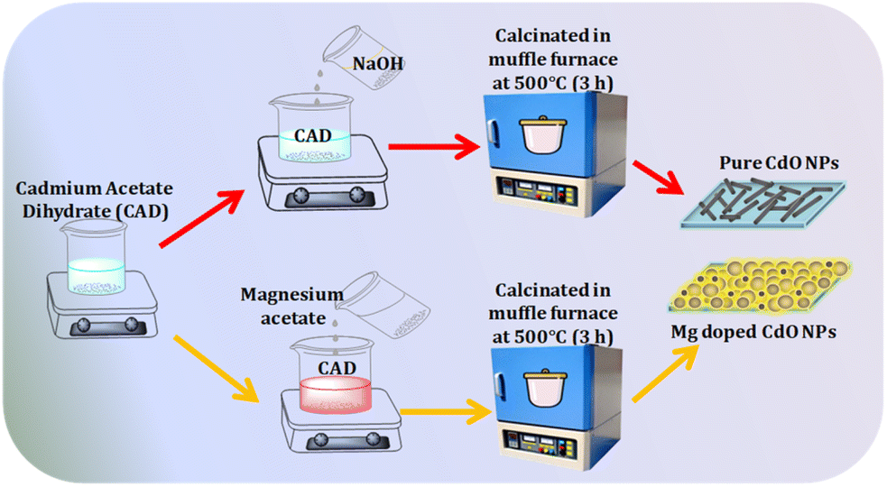 | ||
| Fig. 1 Schematic of co-precipitation synthesis for pure CdO and Mg-doped CdO NPs. | ||
The produced CdO and Mg-doped CdO NPs were then subjected to an array of characterization techniques including XRD, FESEM, TEM, Raman spectroscopy, optical analysis, XPS, and dielectric studies. The goal of these analyses was to thoroughly investigate their crystallization, functional groups, structural and morphological details, and to elucidate their dielectric properties.
3 Results and discussion
3.1 Powder XRD analysis
The crystal structure of the synthesized NPs was analyzed using the powder XRD analysis which was carried out using the Bruker D2 PHASER instrument. Fig. 2(a) illustrates the XRD patterns of both the pure and Mg-doped CdO NPs. The peaks observed at 32.9, 38.3, 55.2, 65.9, and 69.1 degrees corresponded to the (111), (200), (220), (311), and (222) crystal planes, respectively. The observed diffraction peak positions and peak intensity ratios are found to be well-matched with the standard XRD pattern (JCPDS: 75-0592) of CdO such that it could be confirmed that the synthesized CdO NPs are crystallized in the cubic structure with Fm3m (FCC) space group3 and the lattice parameters are a = b = c = 4.77 Å, respectively. The XRD patterns of the Mg-doped CdO exhibit almost the same diffraction pattern over the diffraction angle from 10 to 80 degrees (here it is shown only from 25 to 72 degrees for clarity) as that of the pure CdO, indicating that the Mg-doped CdO NPs are crystallized in the FCC crystal structure.3 The XRD analysis confirms that the crystal structure remains unchanged upon doping. Moreover, all diffraction peaks display sharp and high intensity indicating the crystalline nature of the synthesized NPs without any amorphous phase. Notably, Fig. 2(b) and (c) shows a noticeable shift of the peaks towards the higher diffraction angle side for the Mg-doped CdO NPs compared to the pure CdO NPs which authenticates that the reduction of the crystal unit cell volume is due to Mg doping.3 The ionic radius of the Cd2+ and Mg2+ are identified to be 0.95 and 0.72 Å, respectively. During the doping process, the Mg2+ ions are successively replaced by the Cd2+ in FCC crystal packing and because of the lower size ionic radius of the Mg2+, the net crystal's unit cell volume is slightly reduced. The alterations mentioned above, including the shift in the diffraction peaks and the increase in the width of the planes, slightly influence the degree of crystallinity in such a way that these changes have also strongly affected the typical morphology which in turn influenced the morphology-related functional properties such as optical transmittance and electrical conductivity.1–3 The average crystallite size of both the pure and Mg-doped CdO was determined using the Debye–Scherrer formula, which is expressed as D = 0.9λ/β![[thin space (1/6-em)]](https://www.rsc.org/images/entities/char_2009.gif) cosθ, where D represents the crystallite size, λ denotes the X-ray wavelength (0.154 nm), θ signifies the Bragg diffraction angle, and β represents the full width at half maximum (FWHM). The crystallite sizes of the pure and doped CdO NPs are found to be 23 and 17 nm, respectively. It is noteworthy that the crystallite size of doped CdO is observed to be smaller than that of pure CdO, as depicted in Table 1.
cosθ, where D represents the crystallite size, λ denotes the X-ray wavelength (0.154 nm), θ signifies the Bragg diffraction angle, and β represents the full width at half maximum (FWHM). The crystallite sizes of the pure and doped CdO NPs are found to be 23 and 17 nm, respectively. It is noteworthy that the crystallite size of doped CdO is observed to be smaller than that of pure CdO, as depicted in Table 1.
 | ||
| Fig. 2 XRD patterns of pure and Mg-doped CdO NPs, (a) XRD (b and c) zoomed-in portions of the (d) peak shift difference with respect to crystallographic planes (e) normalized peak intensity ratios and FE-SEM images of the (f–h) pure and (i–k) Mg-doped CdO NPs (l and m) HR-TEM Images of the pure and Mg doped CdO NPs (inset: FFT pattern). | ||
| Sample | Crystallite size (nm) | Lattice constant Å | Micro strain (ε) (×10−3) | Dislocation density (×1015) | Stacking fault (×10−5) | Band gap (eV) |
|---|---|---|---|---|---|---|
| CdO NPs | 23 | 4.7075 | 0.20 | 1.86 | 4.1 | 2.32 |
| Mg-doped CdO | 17 | 4.7003 | 0.26 | 3.19 | 5.3 | 2.24 |
The slight reduction in crystallite size observed with Mg doping could be attributed to the effective substitution of Mg2+ ions at the lattice sites within CdO or to the creation of oxygen vacancies during the synthesis process. Additionally, this decrease in crystallite size may be linked to the formation of defects. The lattice parameter, determined from the dataset, aligns closely with the value of 4.70 Å reported in the literature.18 The slight discrepancy observed in the lattice parameters of CdO upon Mg doping could be attributed to the lower ionic radii of the Mg2+. The observed results of the diffraction angle shift towards higher angles, indicating the presence of compressive strain, ultimately leading to a reduction in lattice parameters. In addition to that, in Fig. 2(d), the values of the diffraction peak shift difference values are provided for the pure and Mg-doped CdO NPs concerning all crystallographic planes. The non-linear values corresponding to the planes disclose that the surface morphology of the Mg-doped CdO NPs is significantly changed. Following this, in Fig. 2(e), the intensity ratio of the pure and Mg-doped CdO NPs is presented and compared with the standard JCPDS card database. As per the standard pattern, the (111) plane has a highly preferred orientation compared to all other planes. The pure CdO NPs have similar logical preferred orientation profiles while the ratio between (111) and (200) is 1.11 which is found to have reduced to 1.05 for the Mg-doped CdO NPs. Based on this observation, the morphology of the pure CdO NPs has changed from rod to sphere shapes.
The Mg-doped CdO NPs exhibit significantly higher values of other parameters such as dislocation density and micro-strain, which could have been caused because of the formation of defects within the crystal structure. The dislocation density and micro-strain is calculated using the formula ε = βcosθ/4 and δ = 1/D2 where is the ε, δ, D represent dislocation density, micro-strain and crystallite size respectively. The structural parameters of diffraction position, d-spacing, grain size, full width at half maximum (FWHM), lattice constant, micro-strain, and dislocation density are determined using the Scherrer equation for the respective materials and are displayed in Table 1.
3.2 Microscopic analysis
The FE-SEM images distinctly show that the pure CdO exhibits interwoven rod-like nanocrystallites dispersed across a wide range of particle sizes (Fig. 2(f)–(h) first row). Upon Mg doping, the morphology of the grains undergoes a significant alteration, characterized by a complete absence of dense rod-shaped CdO particles. Consequently, a majority of the rods are transformed into quasi-spherical nanostructures (Fig. 2(i)–(k) second row). According to the literature, the external chemical energies (like dopants and surfactants) and physical energies (temperature, pressure, shock waves, and gamma rays) are highly capable of inducing significant changes in the surface morphology of the nanocrystalline materials which is based on the static and dynamic recrystallization processes.19,20 In the present case, the Mg doping facilitates the external and different chemical potential environmental conditions during the synthesis process which can significantly affect the nature of the surface morphology of the nanocrystals at a particular temperature point. In addition to that, as in the case of the XRD results, the (111) peak preferred orientation is found to have reduced while doping Mg into the CdO lattice. If the preferred orientation is changed, most probably it will lead to a new surface morphology. Generally, the outcome of crystal shape is the consequence of the sum of factors such as relative surface energy of crystal faces, twin planes, dislocations, type of solvent, impurities, kinetic, etc. The first two factors are just enough to originate a wide scope of crystal habits. Sivakumar et al. reported the morphological transformation from irregular to rod-shape for the L-tyrosine polycrystalline samples and also found the enhancement of the (111) plane while similar kind of results have been observed in silver bromide.19 Moreover, the absorption and replacement ability of the Mg2+ ions to the Cd2+ ions in the CdO lattice is not the same for all the crystallographic planes since different planes have different growth speeds and surface energies. In the presence case, the Mg2+ ions have marginally affected the (111) intensity (refer to the intensity ratio plot in Fig. 2(e)) which influenced the rod-shaped growth into the sphere-shaped (Fig. 2(f)–(h)). FE-SEM image supports the TEM results of pure CdO and Mg-doped CdO NPs, where it shows a rod morphology while Mg-doped CdO NPs have spherical morphology due to the impact of incorporation of Mg concentration of 0.003 M with the calcinations temperature of 500 °C. Fig. 2(l) and (m) shows the TEM images of pure and Mg doped CdO NPs fabricated by the coprecipitation method. It is apparent from the TEM images that pure CdO shows a inter wovened rod-like nanocrystallites were observed with the area of ∼290 nm and a length of 53 nm. Traces of few empty sites are also evident from the TEM image of the undoped sample (Fig. 2(l)). With Mg doping, the grains starts to modify with traces of dense rod shaped into converted into quasi spherical shaped nano-structures as observed with the diameter of ∼45 nm.3.3 Raman studies
Raman scattering stands out as a sensitive and valuable technique for probing and characterizing nanostructures. In Fig. 3(a) and (b), the Raman spectra of both the pure and Mg-doped CdO NPs are presented over the spectral range of 200–1500 cm−1. The pure CdO NPs' Raman spectrum displays a broad feature extending across the wavenumber range of 250 to 450 cm−1, and a weak wide band at 920 cm−1 such that these bands belong to 2(TA) and (LO) Raman bands. The origin of this peak is ascribed to phonon dispersion in CdO which is specifically identified as a 2TA(L) mode.19 Conversely, the emergence of the second weak peak at 925 cm−1 corresponds to the overtone of a 2LO mode occurring at the L- or C-point of the Brillouin zone, serving as strong evidence indicating the formation of nanostructures. According to the selection rules for the NaCl structure, both the transverse optical (TO) and longitudinal optical (LO) modes are dipole-free. Therefore, all observed features in the spectrum can be ascribed to 2nd order Raman scattering processes in CdO. The 2nd order Raman peaks observed arise from overtones and combination modes. All the Raman peaks visible for CdO in Fig. 3(a) and (b) can be linked to its 2nd order Raman spectral phenomena.20 In the case of Mg-doped CdO NPs, the initial broad features covering Raman bands of 2(TA) experience a significant Raman shift which are located at 267 and 395 cm−1, respectively (Fig. 3(c)). The 2(LO) overtones of Raman mode undergo a significant shift towards the higher wavenumber and to be located at 920 cm−1 which may be because of the particle size reduction, particle shape modification as well as unit cell volume reduction.21,22 In addition to that, in the case of Mg-doped CdO NPs, the 2(LO) overtones of Raman mode intensity are significantly reduced whereby the intensity ratio between 2(TA) and (LO) is found to have reduced such that the values are 2 and 2.8 for the pure and Mg-doped CdO NPs. Mg–CdO NPs have a significantly lower particle size compared to the pure CdO NPs which suppresses the Raman scattering signals whereby the second-order peak has much lower intensity which is quite common in Raman scattering phenomena for nanosize materials.23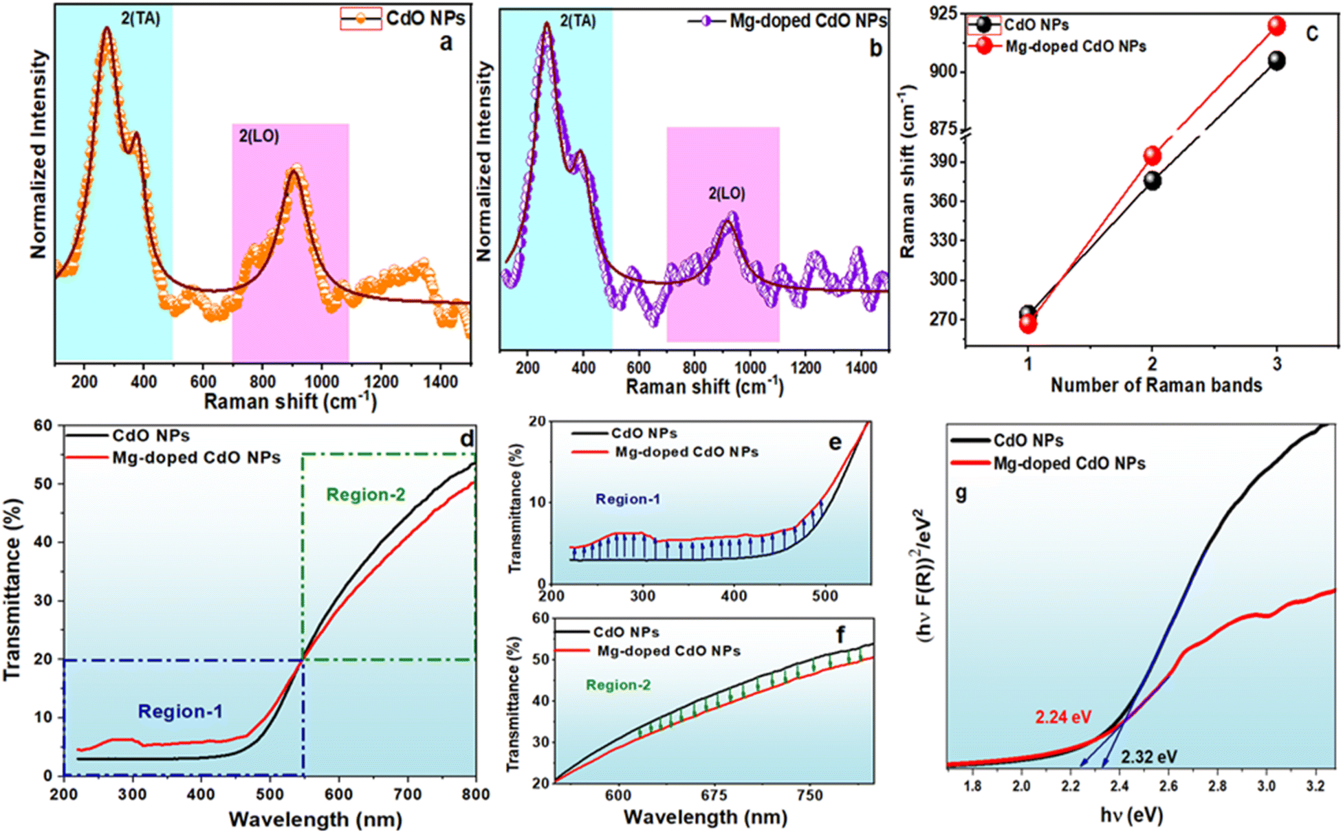 | ||
| Fig. 3 Pure and Mg-doped CdO NPs (a and b) Raman spectra, (c) Raman peak shift profile, (d) optical transmittance, zoomed-in wavelength intervals of (e) 200–550 nm and (f) 550–800 nm, and (g) optical bandgap energy. | ||
3.4 Optical studies
The optical analysis of the synthesized material was conducted through UV-DRS which serves as an effective technique for assessing the light-harvesting capabilities of synthesized semiconductor materials. Fig. 3(d) illustrates the DRS spectra of the fabricated pure and Mg-doped CdO NPs. A prominent absorption peak at 472 nm observed for the pure CdO in the UV region is likely attributable to band-to-band transitions which are well corroborated with the literature reports of the pure FCC structure of CdO NPs.3 The linear optical transmittance profiles of the pure and Mg-doped CdO NPs are portrayed in Fig. 3(d).24 The optical transmittance percentage has linearly increased from the absorption edge region (472 nm) to NIR which is one of the characteristics of CdO's electronic structure.25 The absorption edge occurs because of the interaction between the shallow cores of d states of 4d for Cd and valence band O 2p states.26 There is inversion symmetry at the zone center (0) in the FCC structure where the point group is OH which means that there can be no mixing between O 2p and Cd 4d states at this point because they have different parity.27The Mg-doped CdO NPs exhibit a wide absorption peak around 465 nm within the visible spectrum. Based on the observed absorption peak positions, the Mg-doped CdO NPs undergoes the blue shift which may be due to the particle reshaping as well as particle size reduction. Following the typical peak shift, a significant modification in the optical transmittance percentage could be witnessed in the Mg-doped CdO NPs. The optical transmittance is found to have increased in the region of 200 to 550 nm, and in other regions, it is found a reduction in the optical transmittance and the corresponding zoomed-in profiles are showcased in Fig. 3(e) and (f). The observed changes are quite unique compared to the previously reported results involving transition metal-doped CdO NPs. In semiconductor nanomaterials, the bandgap energy stands as a crucial parameter, which can be determined using the Kubelka–Munk function. This function utilizes the absolute reflectance denoted as R(hν), and its corresponding Kubelka–Munk transformation F[R(hν)]. The values of bandgap energy can be directly derived from F[R(hν)] through the following equation F(R) = (1 − R)2/2R. In this context, the value of “n” is contingent upon the nature of the transition in a semiconductor: n = 1/2 for direct transitions and n = 2 for indirect electron transitions. For CdO, characterized by direct transitions, the value of n is 2. Additionally, “A” represents the proportionality constant. Subsequently, plots were generated between [F(R(hν)) × hν]1/2 and (hν) to assess the band gap. Despite variations in morphology, the synthesized samples exhibit only minimal differences in the values of band gap between 2.32 and 2.24 eV falling within the visible region of the electromagnetic spectrum (Fig. 3(g)). The values of band gap energy decrease upon the incorporation of Mg content, indicating the compatibility of the prepared samples for absorbing visible light. Upon doping, the band gap energy decreases from 2.32 eV to 2.24 eV, a phenomenon likely to be attributed to the defects introduced by Mg doping or the presence of substitutional impurities within the lattice structure of CdO. A higher defect makes the electronic transitions from the filled valence band to the energy level of the defect and it is more probable than the transitions to the conduction band.28 Upon doping Mg into CdO nanopowder samples, a red shift in the energy band gap is observed. This shift can be attributed to the larger atomic radius of Mg compared to Cd, as well as the higher electronegativity of Mg relative to Cd2+. These findings align in line with structural properties, indicating that the inclusion of Mg doping within the Cd structure leads to a reduction in the band gap energy.29,30
3.5 XPS analysis
To ensure the authenticity of the elemental composition within CdO and Mg-doped CdO NPs, the respective XPS spectra were recorded (Fig. 4). The survey XPS spectra of the pure and Mg-doped CdO NPs (Fig. 4(a)) authenticate the exclusive presence of the ingredients of these compounds. Fig. 4. XPS spectra of the pure and Mg-doped CdO NPs (a) survey spectra, (b and c) Cd 3d spectra and (d and e) O 1s spectra. The comparison of the core XPS spectra of Cd and O for the doped and un-doped NPs is shown in Fig. 4(b)–(e) corresponding to the Cd 3d and O 1s peaks and Mg2+ peaks. In pure CdO (Fig. 4(a)), Cd primarily exists as Cd2+, as evidenced by the spin–orbit split peaks of 3d5/2 and 3d3/2 with binding energies at 404.48 and 411.13 eV. The deconvoluted components at higher binding energies at 406.00 and 412.71 eV are identified as surface hydroxyl Cd terminals such as Cd(OH)2 and similar results have been reported.31 For the FCC crystal structure of CdO, the binding energy difference between 3d5/2 and 3d3/2 orbital is found to be around 6.5 to 7 eV.3,31 In the present case, the binding energy difference value is found to be 6.65 eV which is identified to be well-matched with the previous reports.3,31 In the Mg-doped sample, Cd displays similar peaks as in the pure CdO sample, albeit with comparatively lower intensity and minor shift of (0.2 eV) towards the higher binding energy side, signifying the presence of Mg in the CdO sample.32 The Mg 2p spectrum, depicted in Fig. 4(d), illustrates the presence of both the Mg2+ in Mg (Mg2+ at 51.5 eV). In Fig. 4(d) and (e), the XPS spectra of the O 1s region are identified to decipher information regarding absorbed oxygen, lattice oxygen, oxygen vacancies, and surface hydroxyl groups (OH−).31,33 The O 1s spectra display asymmetric peaks, where the lower binding energy peak, approximately at 528.76 eV, could signify lattice O2− ions within the cubic structure, associated with the intrinsic binding energy of oxygen ions in CdO. Conversely, the peak at a higher binding energy, around 531.74 eV is due to the surface hydroxyl components and oxygen deficiency originating from oxygen vacancies. Based on the overall observation, upon Mg doping, the crystal packing and coordination numbers of Cd and O atoms have not changed. For the FCC crystal structure, the Cd and O atoms have six-fold coordination. If the coordination number changes from 6 to higher numbers (7 or 8), the binding energy shift could be observed around 2 eV in the 3d5/2 and 3d3/2 orbital. However, such a large and significant shift is not observed in the present case, and hence it is authenticated that the coronation numbers of Cd and O atoms have not changed by the process of Mg doping. To further validate the previous statement, the binding energy differences have been calculated for the pure and Mg-doped CdO NPs and correlated with the previously reported articles based on the metal ions-doped CdO NPs. Based on the literature, it is obvious that the presence of Mg2+, Ce2+ and Zr4+ ions in the host crystal lattice do not lead any changes in the binding energy difference of 3d5/2 and 3d3/2 orbital whereas, slight changes only be observed in the Al3+ ions.33–35 Using Casa XPS software, atomic percentages were determined. Specifically, for pure CdO, the percentages obtained were 82.63% for Cd and 17.37% for O. In the case of Mg-doped CdO, the atomic percentages for Mg, Cd, and O were found to be 0.5%, 82.05%, and 17.90%, respectively. | ||
| Fig. 4 XPS spectra of the pure and Mg-doped CdO NPs (a) survey spectra, (b and c) Cd 3d spectra and (d and e) O 1s spectra. | ||
3.6 Impedance analysis
To ensure improved electrical contact, silver paint was carefully applied to the faces of the pellet. Subsequently, a parallel plate capacitor was constructed, with the sample acting as the dielectric medium. The response of the dielectric medium was then examined at room temperature. The data collected from these experiments yielded valuable insights into the electric field distribution within the prepared samples.36 Fig. 5(a) depicts the changes in the values of the dielectric constant of the pure and Mg-doped CdO samples as the frequency increases. The dielectric constant is primarily influenced by the chemical structure, composition, and level of polarization within the material. In this context, the observed variation in the dielectric constant with increasing applied frequency indicates that it is higher in the low-frequency range and diminishes as the frequency rises. Additionally, in the higher frequency range, the value remains relatively constant. The phenomenon can be elucidated through the dielectric polarization mechanism inherent in the material. Dielectric polarization manifests in various forms such as electronic, ionic, interfacial, or dipolar polarization. Electronic and ionic polarizations predominantly occur at high frequencies, whereas the other two mechanisms dominate at low frequencies. The high dielectric constant values observed at lower frequencies are attributed to interfacial polarization, wherein space charges formed within the material induce similar charges on the electrodes. Under the influence of an effective electrical field, these migrating space charges become trapped by defects, leading to the localized accumulation of charge at the interface between the electrode and the sample.37 Additionally, moving charged particles like electrons traverse through these grain boundaries from one interstitial site to another, establishing a barrier through the application of a hopping conduction mechanism. Within these grain boundaries, the resistance encountered by electrons exceeds that of the induced polarization arising from the high dielectric constants. This observed phenomenon aligns with the principles outlined in the Maxwell–Wagner two-layer model. Under high-frequency conditions, the mobility of electrons within these grain boundaries decreases, leading to a reduction in the dielectric constant value in the high-frequency range. The impact of Mg doping is evidenced by an increase in the dielectric constant value, particularly noticeable in the low-frequency range. This increment alters the intrinsic dielectric properties and induces structural modifications as a consequence of Mg doping.38 The dissipation of electrical energy within a material, known as dielectric and tangent loss, occurs as a result of electrical conduction, dielectric relaxation, dielectric resonance, and non-linear loss phenomena. Dielectric loss can generally be categorized into two main types: intrinsic loss and extrinsic loss. Intrinsic loss can be attributed to factors like the symmetry of the crystals, the frequency of the alternating current (AC) field, and the temperature of the experimental setup. Conversely, extrinsic loss is often influenced by various parameters such as impurities within crystals, disordered crystal structures, and arbitrary orientations within crystalline materials. Dielectric and tangent loss for the pure and Mg-doped CdO NPs as a function of frequency is illustrated in Fig. 5(b). It is evident from Fig. 5(b) that the dielectric loss follows the analogous trends as the dielectric constant. Specifically, its value is higher in the low-frequency range and decreases as the frequency increases. The decline in dielectric loss with frequency can be attributed to several factors, including the inhibition of domain wall movement and space charge polarization. These alterations lead to a decrease in dielectric loss in the high-frequency region. The fluctuation in dielectric loss concerning the Mg dopant content suggests a considerably higher dielectric loss in the doped material compared to the undoped material. The increase in dielectric loss associated with the dopant content may be elucidated by the presence of notable oxygen vacancies, the mechanism of hopping conduction, increased resistance introduced by the electrode, and the presence of grain boundaries. Materials characterized by high dielectric constants and lower loss exhibit minimal leakage current, rendering them promising candidates for various applications including microwave technology, energy storage, communication systems, microstrip antennas, and high-frequency devices.
 | ||
| Fig. 5 Variation of frequency dependent behaviour of pure and Mg-doped CdO NPs including (a) dielectric constant (b) dielectric loss, (c) z′, (d) z′′, (e) Nyquist plot and (f) Jonscher's power law. | ||
3.7 Complex impedance and electrical conductivity analysis
Fig. 5(c) and (d) depicts z′ and z′′ of the complex impedance plotted against frequencies. The graphs show a gradual decrease in the magnitude of z′ values for both Mg-doped and undoped CdO NPs samples as frequency and Mg content increase in the material, indicating an increase in AC conductivity. Besides, the decrease in z′ values is ascribed to the increased mobility of charged carriers within the material. The frequency-independent behavior of z′ observed in the high-frequency region can be explained by the release of space charge resulting from the diminished barrier properties of the materials (Fig. 5(c)). Analogous to the variation observed in z′, the behavior change of z′′ for the title material is evident.As frequency increases z′′ rises to a maximum value before gradually decreasing (Fig. 5(c). Notably, the frequency (fmax) at which each sample reaches its maximum z′′ value differs, with this frequency value shifting towards the high-frequency region, indicating relaxation within the test material. Concurrently, the intensity of the peaks decreases, while their width increases with the addition of Mg content in CdO NPs. The presence of electrons or stable materials accounts for the intense and narrow peaks observed in CdO NPs, while the lower intensity and broader peaks in Mg-doped CdO NPs can be attributed to the presence of impurities and defects. Additionally, the decrease in the amplitude of z′′ and eventual merging of peaks at high frequencies, may be attributed to the release of spatial charges within the material.39 The Nyquist plot provides insights into both intrinsic and extrinsic contributions, including the effects of grains, grain boundaries, and electrode interfaces on the material's conductivity (Fig. 5(d)). As observed in the Nyquist plot, the horizontal and vertical values of the graphs vary, indicating that the samples with different doping ions may exhibit semicircular patterns with unique horizontal and vertical values. In Fig. 5(d)), the arc observed for the pure CdO NPs has a larger diameter compared to that of the doped NPs, indicating a lower efficiency in charge transfer for the pure NPs. It is evident that impedance decreases with increasing frequency, likely due to the dielectric properties of the material. The addition of Mg dopant reduces the electrical resistance of the material, leading to a decrease in electrical resistance with higher dopant content. It could be because of the increased hopping conduction mechanism in the Mg-doped CdO NPs sample. The substitution of Mg contents with Cd contents induces structural defects and tunes the bandgap. In short, the material with less electrical resistance has good potential to be applied in different electronic devices.38 Moreover, the R–C equivalent circuit, simulated through ZSimpWin software (version 3.20), accurately represents the semicircular arcs as observed. Despite only one depressed semicircular arc being present in the material under investigation, the impedance primarily reflects the contribution of grains rather than other factors. Analysis of the impedance data for the material reveals that the R(CR)(CR) circuit provided the most optimal fit among various circuit models, as depicted in Fig. 5(d). Fig. 5(d) confirms the appropriateness of selecting this equivalent circuit, as it demonstrates a close match between experimental observations and the fitted values. The AC conductivity characteristics of both the title materials are illustrated in Fig. 5(e). It is noted that the AC conductivity increases proportionally with frequency (ranging from 1 Hz to 1 MHz) and with the presence of Mg dopant in the material. The Mg-doped sample exhibits enhanced electronic conductivity, facilitating easier electron transfer, thereby resulting in higher polarization compared to the undoped sample. The unique characteristics exhibited by the doped sample are attributed to dispersion, relaxation, and reorientation phenomena, as outlined in the hoping relaxation model. Additionally, the conductivity can be accurately described by the equation σac = σdc + Aωn, known as Jonscher's power law. Here, σdc denotes the frequency-independent conductivity, while the term Aωn represents the frequency-dependent AC conductivity. Moreover, in the equation, the constant “A” is temperature-dependent and provides insights into polarization, while “ω” represents frequency, and “n” is a frequency-dependent exponent factor ranging between 0 and 1. When “n” is ≤1, it indicates that mobile charge carriers undergo translational motion, albeit with a pronounced hoping effect, leading to direct current (dc) conduction. Conversely, when “n” exceeds 1, alternating current (ac) conduction governs the behavior of localized mobile charge carriers.38,40 It is noteworthy that Table 2 displays the computed values of σdc, A, n, and R2, acquired through data fitting using the aforementioned relationship. In this dataset, the exponent ‘n’ consistently maintains a value of 0.70, while the σdc value exhibits an increase from 1.40 × 10⁻⁹ to 2.90 × 10⁻⁹.
| Room temperature | CdO NPs | Mg-doped CdO NPs | |
|---|---|---|---|
| σdc (S cm−1) | 1.40 × 10⁻⁹ | 2.90 × 10⁻⁹ | |
| A | 4.04 × 10⁻¹¹ | 8.09 × 10⁻¹¹ | |
| n | 0.7 | 0.7 | |
| σac (S cm−1) | 50 Hz | 2.26 × 10⁻⁹ | 4.53 × 10⁻⁹ |
| 100 Hz | 3.67 × 10⁻⁹ | 7.35 × 10⁻⁹ | |
| 1 kHz | 1.84 × 10⁻⁸ | 3.69 × 10⁻⁸ | |
| 10 kHz | 9.22 × 10⁻⁸ | 1.85 × 10⁻⁷ | |
| 1 MHz | 2.32 × 10⁻⁶ | 4.64 × 10⁻⁶ | |
| σtotal | 50 Hz | 3.66 × 10⁻⁹ | 7.43 × 10⁻⁹ |
| 100 Hz | 5.07 × 10⁻⁹ | 1.03 × 10⁻⁸ | |
| 1 kHz | 1.98 × 10⁻⁸ | 3.98 × 10⁻⁸ | |
| 10 kHz | 9.36 × 10⁻⁸ | 1.88 × 10⁻⁷ | |
| 1 MHz | 2.32 × 10⁻⁶ | 4.64 × 10⁻⁶ | |
| R2 | 0.9996 | 0.9997 | |
4 Conclusions
In conclusion, both pristine and Mg-doped CdO NPs were effectively synthesized through the co-precipitation method. The incorporation of Mg has been validated to induce a decrease in crystallite size as evidenced by XRD analysis. Morphologically, FE-SEM and TEM has vividly captured the transition from elongated rods to quasi-spherical forms a direct consequence of Mg dopant. This morphological reinvention is mirrored in the optical domain where transmittance spectrum shifts and a decrement in optical band gap energy are observed. Furthermore, Raman and XPS corroborate the integration of Mg, adding to the lattice with discernible peak shifts. Dielectric spectroscopy unveils an increased dielectric constant and electrical conductivity in Mg-doped CdO NPs. The collective insights derived from this study not only enrich the foundational knowledge of doping mechanisms but also position Mg-doped CdO NPs as a viable and innovative candidate for semiconductor applications.Data availability
We confirm that the data supporting the findings of this work are available within the main article.Author contributions
S. Cathrin Lims: validation, formal analysis, resources and writing – original draft. M. Jose: formal analysis, review & editing, Sivakumar Aswathappa: validation, formal analysis and resources. S. Sahaya Jude Dhas: review & editing. Raju Suresh Kumar: resources. Phuong V. Pham: supervision, writing – review & editing.Conflicts of interest
The authors declare that they have no conflict of interest.Acknowledgements
This work is supported by the National Science and Technology Council (Grant No. NSTC-112-2112-M-110-004-MY3), Taiwan. This project was also supported by Researchers Supporting Project number (RSP2024R231), King Saud University, Riyadh, Saudi Arabia.Notes and references
- C. Kinnear, T. L. Moore, L. Rodriguez-Lorenzo and B. Rothen-Rutishauser, Chem. Rev., 2017, 117, 11476–11521 CrossRef CAS
.
- M. Malik, M. A. Iqbal, M. Malik, M. A. Raza, W. Shahid, J. R. Choi and P. V. Pham, Nanomaterials, 2022, 12, 616–623 CrossRef CAS
- S. Aswathappa, L. Dai, S. J. J. Dhas, S. B. Dhas, S. Laha, R. Kumar and A. Almansour, Inorg. Chem., 2024, 63, 576–592 CrossRef CAS PubMed
- M. Malik, M. A. Iqbal, Y. Iqbal, M. Malik, S. Bakhsh, S. Irfan, R. Ahmad and P. V. Pham, Inorg. Chem. Commun., 2022, 145, 109980–109989 CrossRef CAS
- H. Zhang, Z. Ji, T. Xia, H. Meng, C. Low-Kam and R. Liu, ACS Nano, 2012, 6, 4349–4368 CrossRef CAS
- D. H. Nhan, H. N. Cong, N. N. T. Nha, L. P. Hai, N. T. Toan, H. L. Cuong, S. W. Kim, P. V. Pham, L. T. Lu, L. V. Hieu and T. K. Le, J. Nanopart. Res., 2024, 26, 90–97 CrossRef CAS
- M. B. A. Bashir, E. Y. Salih, A. H. Rajpar, G. Bahmanrokh and M. F. M. Sabri, J. Manuf. Syst., 2022, 32, 085006–085034 CAS
- R. J. Guerrero-Moreno and N. Takeuchi, Phys. Rev. B: Condens. Matter Mater. Phys., 2002, 66, 205205–205234 CrossRef
- P. V. Pham, S. C. Bodepudi, K. Shehzad, Y. Liu, Y. Xu, B. Yu and X. Duan, Chem. Rev., 2022, 122, 6514–6613 CrossRef CAS PubMed
- P. Kumar, M. C. Mathpal, G. K. Inwati, S. Ghosh, V. Kumar and W. D. Roosa, Colloids Surf., A, 2020, 605, 125369–125382 CrossRef CAS
- S. C. Lims, S. Divya, V. Abirami, K. Kasinathan and M. Jose, J. Mater. Sci. Eng. B, 2024, 300, 117077–117089 CrossRef
- K. Usharani, A. R. Balu, V. Nagarethinam and M. Suganya, Prog. Nat. Sci.: Mater. Int., 2015, 25, 251–257 CrossRef CAS
- P. Umarani, K. Sivakumar, S. Sathiya, S. C. Lims, S. Aswathappa, R. S. Kumar, A. I. Almansour and S. S. J. Dhas, Opt. Mater., 2024, 149, 115126–1151242 CrossRef CAS
- Y. Yang, S. Jin, J. Medvedeva, J. Ireland, A. Metz, J. Ni and M. Hersam, J. Am. Chem. Soc., 2005, 127, 8796–8804 CrossRef CAS PubMed
- N. Manjula, M. Pugalenthi, V. Nagarethinam, K. Usharani and A. R. Balu, Mater. Sci., 2015, 33, 774–781 CAS
- R. K. Gupta, K. Ghosh, R. Patel and P. K. Kahol, Appli. Surf. Sci., 2009, 255, 4466–4469 CrossRef CAS
- C. Liu, Y. Foo, M. Kamruzzaman, C. Y. Ho, J. Zapien, W. Zhu, Y. Li, W. Walukiewicz and K. Yu, Phys. Rev. Appl., 2016, 6, 064018–064039 CrossRef
- Leelavati, R. Kumar and R. Kumar, Appl. Phys. A: Mater. Sci. Process., 2023, 129, 604 CrossRef CAS
- S. Aswathappa, L. Dai, S. S. J. Dhas, S. A. M. B. Dhas, K. K. Bharathi, R. S. Kumar and A. I. Almansour, CrystEngComm, 2024, 26, 1199–1207 RSC
- X. Lü, Q. Hu, W. Yang, L. Bai, H. Sheng, L. Wang, F. Huang, J. Wen, D. J. Miller and Y. Zhao, J. Am. Chem. Soc., 2013, 135, 13947–13953 CrossRef
- N. Millan, N. Dewit and C. Van Roost, Phys. Chem. Chem. Phys., 2000, 2, 171–175 RSC
- M. Ravikumar, R. Chandramohan, D. A. K. Karuppiah, S. Valanarasu, V. Ganesh, M. Shkir, S. AlFaify and A. Kathalingam, Bull. Mater. Sci., 2019, 42, 1–10 CrossRef CAS
- V. Ganesh, L. Haritha, H. E. Ali, A. M. Aboraia, Y. Khairy, H. H. Hegazy, V. B. Alexander, V. Soldatov, H. Algarni, H. Y. Zahran and I. S. Yahia, Appl. Phys. A: Mater. Sci. Process., 2020, 126, 551–572 CrossRef CAS
- C. Y. Xu, P. X. Zhang and L. Yan, J. Raman Spectrosc., 2001, 32, 862–865 CrossRef CAS
- S. D. S. Santos, W. Paraguassu, M. Maczka and P. T. C. Freire, Spectrochim. Acta, Part A, 2017, 174, 80–85 CrossRef PubMed
- Y. Zhao, K. T. E. Chua, C. K. Gan, J. Zhang, B. Peng, Z. Peng and Q. Xiong, Phys. Rev. B: Condens. Matter Mater. Phys., 2011, 84, 205330–205343 CrossRef
- R. J. Guerrero-Moreno and N. Takeuchi, Phys. Rev. B: Condens. Matter Mater. Phys., 2002, 66, 205 CrossRef
- W. Raza, S. Faisal, M. Owais, D. Bahnemann and M. Muneer, RSC Adv., 2016, 6, 78335–78350 RSC
- X. Chen, P. Zhou, H. Yan and M. Chen, Energy, 2021, 216, 119254–119266 CrossRef CAS
- M. W. Maswanganye, G. L. Kabongo, L. E. Mathevula, B. M. Mothudi and M. S. Dhlamini, Sci. Rep., 2023, 13, 20131–20144 CrossRef CAS PubMed
- H. Khallaf, C.-T. Chen, L.-B. Chang, O. Lupan, A. Dutta, H. Heinrich, A. Shenouda and L. Chow, Appl. Surf. Sci., 2011, 257, 9237–9242 CrossRef CAS
- K. Sankarasubramanian, K. J. Babu, P. Soundarrajan, T. Logu, G. Gnanakumar, K. Ramamurthi, K. Sethuraman and S. Kumar, Sens. Actuators, B, 2019, 285, 164–172 CrossRef CAS
- D. J. Jeejamol, K. S. J. Aultrin and M. D. Anand, Opt. Quantum Electron., 2022, 54, 291–307 CrossRef CAS
- K. Mohanraj, D. Balasubramanian, K. Porkumaran, N. Jhansi and J. Chandrasekaran, J. Mater. Sci.: Mater. Electron., 2018, 29, 20439–20454 CrossRef CAS
- D. J. Jeejamol, A. M. E. Raj, K. Jayakumari and C. Ravidhas, J. Mater. Sci.: Mater. Electron., 2018, 29, 97–116 CrossRef CAS
- V. A. Hastir, S. Sharma and R. Singh, Appl. Surf. Sci., 2016, 372, 57–62 CrossRef
- F. Rubio-Marcos, P. Marchet, X. Vendrell, J. Romero, F. Rémondière, L. Mestres and J. F. Fernández, J. Alloys Compd., 2011, 509, 8804–8811 CrossRef CAS
- F. Bibi, S. Iqbal, H. Sabeeh, T. Saleem, B. Ahmad, M. Nadeem, I. Shakir, M. Aadil and A. Kalsoom, Ceram. Int., 2021, 47, 30911–30921 CrossRef CAS
- K. Shamim, S. Sharma, S. Sinha and E. Nasreen, J. Adv. Dielectr., 2017, 7, 1750020–1750037 CrossRef
- S. C. Lims, S. Divya, K. K. Bharathi, G. Viju, S. J. Das and M. Jose, J. Mater. Sci. Eng. B, 2023, 289, 116235–116245 CrossRef
| This journal is © The Royal Society of Chemistry 2024 |