
 Open Access Article
 This Open Access Article is licensed under a
 Creative Commons Attribution 3.0 Unported Licence
2H-SnS2 assembled with petaloid 1T@2H-MoS2 nanosheet heterostructures for room temperature NO2 gas sensing†
Shraddha Hambirae,
Shashikant Shindeb,
H. M. Pathana,
Som Datta Kaushikc,
Chandra Sekhar Rout d and
Shweta Jagtap*e
d and
Shweta Jagtap*e
aDepartment of Physics, Savitribai Phule Pune University, India
bMES's Department of Physics, Nowrosjee Wadia College, Pune 411001, India
cUGC-DAE Consortium for Scientific Research Mumbai Centre, BARC, Mumbai, India
dCentre for Nano and Material Sciences, Jain (Deemed-to-be University), Jain Global Campus, Ramanagaram, Bangalore, India
eDepartment of Electronic and Instrumentation Science, Savitribai Phule Pune University, India. E-mail: shweta.jagtap@gmail.com
First published on 1st August 2024
Abstract
In this study, we explored the gas-sensing capabilities of MoS2 petaloid nanosheets in the metallic 1T phase with the commonly investigated semiconducting 2H phase. By synthesizing SnS2 nanoparticles and MoS2 petaloid nanosheets through a hydrothermal method, we achieve notable sensing performance for NO2 gas at room temperature (27 °C). This investigation represents a novel study, and to the best of our knowledge no, prior similar investigations have been reported in the literature for 1T@2HMoS2/SnS2 heterostructures for room temperature NO2 gas sensing. The formed heterostructure between SnS2 nanoparticles and petaloid MoS2 nanosheets exhibits synergistic effects, offering highly active sites for NO2 gas adsorption, consequently enhancing sensor response. Our sensor demonstrated a remarkable sensing response (Ra/Rg = 7.49) towards 1 ppm of NO2, rapid response time of 54 s, baseline recovery in 345 s, good selectivity and long-term stability, underscoring its potential for practical gas-sensing applications.
1 Introduction
Emission of harmful gases from various sectors such as transportation, agriculture manufacturing, construction and power generation affect both human health and the environment. To address this issue, severe regulations are being implemented globally to restrict the emission of air pollutants.1,2 Among these gases, NO2 is well known for being the most harmful gas to the entire ecosystem. If NO2 concentration exceeds 53 ppb, it can lead to serious health issues such as, lung disease, pulmonary irritations, chronic diseases etc. Hence, it is important to keep track of a number of gases in our surroundings on a regular basis3,4 and it is highly important to develop a cost-effective gas detection device that is efficient, precise and highly sensitive and selective.Several methods are available for detection of toxic gases, including chemiresistive, calorimetric, optical, and electrochemical techniques.5 However, few methods encounter challenges like limited accessibility, higher costs, and sensitivity constraints etc. Resistive gas sensors have garnered considerable interest due to their compact size, ease of fabrication, straightforward operation, and cost-effectiveness in manufacturing.6,7 Metal oxide semiconductors (MOS) have served as effective gas sensors in the past, but their reliance on high operating temperatures led to increased power consumption. Lately, two-dimensional (2D) layer-structured materials have gained significant interest across several domains.8 Notably, two-dimensional semiconductor materials distinguish themselves through their extensive band gap coverage, interface free of dangling bonds, high mobility, and rapid carrier transport. A high specific surface area and rich active sites make it possible to adsorbed a large number of gas molecules, which is one of the best properties that make 2D structures advantageous in gas sensing applications.9 In addition, the electrical characteristics of 2D materials can be modulated by altering the number of layers.10 These materials undoubtedly provide a reasonably good foundation for developing high-performance gas sensors.9 In particular, tin disulfide (SnS2), a characteristic 2D layered material with weak van der Waals interactions between its layers has received significant interest.11 The non-solubility and non-toxicity of SnS2 in aqueous solutions make it a very promising material. SnS2 is characterised by its unique structure at the atomic layer level, which results in an abundance of available functional active sites.12 Being a more electronegative nanomaterial, SnS2 accumulates chemically adsorbed molecules on its surface, generating an electrostatic potential. The depletion region of this surface potential corresponds to the size of the entire nanostructure. This unique attribute of n-type SnS2 nanosheets enhances gas adsorption sites, making it a strong option for designing and making high-performance NO2 gas monitors.12,13 Moreover, the two-dimensional surface of SnS2 is favourable for incorporation other semiconductors, which results in the formation of well-contacted heterojunctions that improve carrier conduction.14,15 It has been found that the formation of heterojunctions is a highly effective method for manipulating the electronic state of the SnS2 surface, thereby substantially enhancing its gas sensing characteristics.16 Comparing heterojunction materials to individual materials, they often perform better due to their diverse morphologies and band alignments. This improvement may be linked to the excellent heterointerface, which promotes fast charge transfer. Furthermore, the curved shape of the conductive band and the valence band in a typical heterojunction structure often causes the Fermi level to attempt equilibrium, which ultimately leads in the formation of a depletion layer. This effect reduces response and recovery times by directly contributing to high conductivity.16,17 The construction of two-dimensional heterojunction nanomaterials has been a popular and advanced method for designing gas sensors in recent years. Similar to SnS2, MoS2 possesses a traditional layer arrangement with weak van der Waals interactions.15 Therefore, the development of improved heterointerfaces by employing 2D SnS2 and MoS2 nanosheets stands as a promising approach for further improving electrical capabilities. Furthermore, the metastable 1T phase exhibits superior electrical conductivity for charge transfer and higher adsorption energy to NOx compared to the semiconducting 2H phase, suggesting its suitability for gas sensing applications. For example, MoS2 nanosheets coated with SnS2 nanoparticles (MoS2/SnS2) were developed by Jia-Bei Liu and colleagues by using the simple hydrothermal process and mechanical exfoliation method. The results of this study indicated that the SnS2 nanoparticles, which serve as an efficient antioxidative decoration, may increase the stability of MoS2 nanosheets. This provides a potential way to create high-stability NO2 gas sensors at ambient temperature.18
Considering the synergistic effects of heterostructures to boost gas sensing performance. This novel investigation explored the 1T@2H MoS2/SnS2 heterostructure by a simple hydrothermal approach to construct a two-dimensional layered 2H-SnS2 decorated on petaloid 1T-MoS2 nanosheets for room temperature NO2 gas sensing, marking the first instance of such research in the literature without prior similar studies. Utilizing a range of characterization techniques, comprehensive structural and functional investigations were conducted on the synthesized material. The hierarchical structure of the SnS2/MoS2 sensor proved superior to the pristine SnS2 sensor, exhibiting good response (Rg/Ra = 7.49) to 1 ppm NO2 at ambient temperature. The sensor is particularly noteworthy for its excellent selectivity and consistent repeatability.
2 Experimental
2.1 Synthesis of SnS2 nanoparticles
SnS2 nanoparticles were synthesized using a one-pot hydrothermal process. The procedure involved 0.7 gm of SnCl4·5H2O, added in 30 ml of deionized water with stirring until a clear solution was formed. Subsequently, 1.2 g of CH3CSNH2 was added to the above solution, and the mixture was stirred for ten minutes. The resulting solution was then transferred to a 50 ml stainless steel autoclave lined with Teflon. Then the autoclave was maintained at 180 °C for 24 hours to facilitate the formation of SnS2 nanomaterials, followed by centrifugation, the precipitates subsequently subjected to overnight drying at 60 °C to obtain the final product.2.2 Synthesis of 1T@2H-MoS2/SnS2 heterostructures
SnS2/MoS2 heterostructures were also formed by a hydrothermal process. To produce a uniform suspension of SnS2, 0.2 g of SnS2 was introduced to 90 ml of deionized water and ultrasonicated for 5 minutes. Later SnS2 solution was mixed vigorously for two hours with addition of 1.79 g of ammonium molybdate ((NH4)6Mo7O24·2H2O), 0.68 g of CH3CSNH2, and 0.885 g of C19H42BrN. Following that, the prepared mixture was transferred into a Teflon-lined stainless-steel autoclave with a volume of 180 ml which was then subjected to heating at 180 °C for a duration of 24 hours. After cooling to room temperature, the final product was thoroughly washed multiple times with deionized water, ethanol and dried at 60 °C. For synthesis of MoS2 similar procedure were carried out without addition of SnS2.2.3 Material characterization
X-ray powder diffraction (XRD) analysis was performed using a Bruker D8 Advance instrument with Cu-Kα radiation (λ = 0.15406 nm). The investigation covered a range from 5° to 80° (2θ) to identify the crystal phase structures of the samples. The optical spectra of the material were obtained using a UV-vis spectrometer (Jasco V750). Additionally, the morphology of the synthesized material was examined through field emission scanning electron microscopy (FESEM) using a FET Nova Nano SEM 450. The current–voltage (I–V) characteristics of the semiconductor were assessed using a semiconductor parameter analysers system, (Keithley 4200A). X-ray photoelectron spectroscopy (K alpha + X-ray photo spectrometer with X-ray source – Al K). The spectra were analyzed using the XPSpeak41 software. The core peaks were deconvoluted and identified with the help of literature. The analysis of the specific surface area and pore size distribution of the synthesized material was done using the Brunauer–Emmett–Teller (BET) model and the Barrett–Joyner–Halenda (BJH) technique respectively.2.4 Gas sensor fabrication and gas sensing measurement
For the gas sensing test, a gold electrode was deposited on a 1 cm by 1 cm alumina substrate through the thermal evaporation method. The device features interdigitated electrodes (IDEs) designed to facilitate gas detection. It includes two main electrodes, each 0.6 cm in length, separated by a distance of 0.4 cm. The interdigitated pattern comprises parallel fingers from each electrode, interleaved with one another. Each finger in the IDE is 0.04 cm wide, with a gap of 0.02 cm between adjacent fingers. The dimensions of the sensing film are illustrated in the ESI (Fig. S1).† Film fabrication was carried out using the drop-casting method. A suitable quantity of the synthesized material was dispersed in 5 ml of ethanol by ultrasonication for about 10 minutes. Subsequently, 10 μl of the obtained dispersion was placed at the centre of the alumina substrate, which had pre-printed interdigital gold electrodes. Gas sensing measurements were conducted using a tabletop gas sensing unit, as reported in the literature.19,20 We utilized a piston cylinder with a capacity of 500 ml containing a gas at a concentration of 1000 ppm. To calculate the volume required to achieve a concentration of 1 ppm in a 250 ml chamber, we applied the dilution formula:| C1V1 = C2V2 |
Therefore, to achieve a 1 ppm concentration in a 250 ml chamber, we need 0.25 ml of gas from the cylinder. We then used syringe to collect 0.25 ml of the gas from the 1000 ppm cylinder.
3 Result and discussion
3.1 Structure and morphology
Using X-ray diffraction (XRD), the crystal structure and phase purity of the synthesized materials were evaluated. Fig. 1 illustrates the XRD pattern of the as-prepared MoS2, and 1T@2H-MoS2/SnS2 heterostructures. Fig. 1a shows diffraction peaks at 2θ = 8.67°, 17.72°, 32.28°, 34.55°, and 56.51°, which correspond to the crystal planes (002), (004), (100), (103), and (110) of 1T@2H-MoS2 (JCPDS, No. 37-1492) further it was also observed that the peak appeared at 2θ = 8.67 i.e. (002) plane have significant displacement from 14° to 8.67°, suggesting that the interlayer spacing in 1T-MoS2 was greater than in 2H-MoS2. This shift is likely attributed to the intercalation of ammonium ions.21 Fig. 1b shows an XRD pattern with two separate sets of peaks, one for MoS2 petaloid nanosheets and the other for SnS2 nanoparticles. XRD pattern of the as-prepared SnS2 nanoparticles is illustrated in Fig. S2.† Diffraction peaks at 8.89°, 17.95°, and 56.66°, which correspond to the (002), (100), and (110) planes of 1T@2H-MoS2 in the SnS2/MoS2 composite. In addition to this peak at 15.08°, 33.30° and 52.50° corresponds to the (001), (101) and (111) crystallographic planes of SnS2. Findings suggested the integration of both materials into a mixed lattice. Slight shifts in the SnS2 peaks towards lower angles and the MoS2 peaks towards higher angles indicated the presence of heterostructures qualities between MoS2 and SnS2.22 | ||
| Fig. 1 XRD diffraction patterns of (a) 1T@2H-MoS2, (b) 1T@2H-MoS2/SnS2 heterostructures. | ||
X-ray Photoelectron Spectroscopy (XPS) measurements were performed to determine the presence of the 1T@2H-MoS2 mixed phase and to examine the bonding arrangement, chemical composition, and electronic structure. The entire XPS spectrum of a SnS2-decorated MoS2 heterostructures in Fig. 2a shows Sn, Mo, S, and tiny quantities of carbon and oxygen. The presence of oxygen is a result of ambient oxygen adsorption on the composite surface. In Fig. 2b two prominent peaks, corresponding to Mo 3d5/2 and Mo 3d3/2 at around 228.9 and 231.84 eV, respectively, in the XPS spectra of the Mo 3d region for the SnS2/1T@2H-MoS2 composite show the existence of the 1T phase of MoS2. Two smaller 2H phase peaks with binding energies at 229.9 and 233.2 eV shift by about 1 eV to higher binding energies than 1T-MoS2.23–26 This change indicates the presence of a trace quantity of semiconducting MoS2 in the 2H phase. The +6-oxidation state of Mo (Mo6+ 3d3/2) is responsible for another weak peak at 236.9 eV which shows that pure MoS2 is partially oxidized. High-resolution S 2p spectra (Fig. 2c) show two peaks at 160.82 and 162.51 eV for S 2p1/2 and S 2p3/2 of S2− from MoS2 one unidentified peak were observed at 160.03. The SnS2/MoS2 heterostructures is further confirmed by two distinctive peaks in the S 2p spectra of SnS2/MoS2 that are located at 160.40 and 163.47 eV, respectively and correspond to S2− 2p1/2 and S2− 2p3/2 from SnS2.27 In the Sn 3d region from Fig. 2d, the peaks at 487.5 eV and 496.1 eV are typical Sn(IV) peaks. Interestingly, two more peaks at 485.2 eV and 493.6 eV suggest that Sn has changed in chemical states, which may be due to SnS2 and MoS2 interactions.28
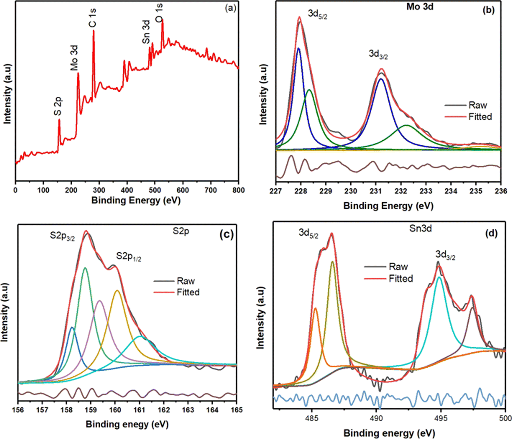 | ||
| Fig. 2 (a) XPS survey spectra of SnS2/1T@2H-MoS2 heterostructures, high resolution XPS spectra of (b) Mo 3d. (c) S 2p. (d) Sn 3d. | ||
The microstructures of 1T@2H-MoS2 and its heterojunction with SnS2 were investigated using Field Emission Scanning Electron Microscopy (FESEM). Fig. 3a shows pristine 1T@2H-MoS2, which features a combination of small nanoparticles and petaloid nanosheets ranging from 1–3 μm in length. High-resolution Fig. 3b reveals small pores on the petaloid nanosheets and width of the nanosheets is around 30–80 nm. Pure SnS2, illustrated in Fig. S4(a),† consists of closely packed small nanoparticles. The pristine 1T@2H-MoS2 also displays some nanoparticle morphology, whereas in the composite, as shown in Fig. 3c, spherical SnS2 particles developed on the surface of the porous 1T@2H-MoS2 petaloid nanosheets. Fig. 3d shows that the significant aggregation of the SnS2 nanoparticles, resulting in the formation of a small sheet-like structure. Fig. 3e showed TEM image of 1T@2H-MoS2/SnS2 which consist of SnS2 and MoS2 nanoparticles which are around 10 to 20 nm in size, along with MoS2 nanosheets. Further to confirm the presence of nanoparticles and petaloid nanosheets in 1T@2H-MoS2/SnS2, EDS analysis was also carried out as shown in Fig. 3f which clearly shows presence of sulfur (S), molybdenum (Mo), and tin (Sn) elements. Individual elemental distribution is also shown in Fig. 3g–i for Mo, Sn and S respectively.
 | ||
| Fig. 3 FESEM images of (a and b) 1T@2H-MoS2, (c and d) 1T@2H-MoS2/SnS2, (e) TEM image 1T@2H-MoS2/SnS2, (f–i) EDS mapping of 1T@2H-MoS2/SnS2 heterostructures. | ||
 | ||
| Fig. 4 (a) N2 adsorption–desorption isotherms of pure 1T@2H-MoS2 and 1T@2H-MoS2/SnS2 heterostructures, sensor response of, (b) SnS2, (c) 1T@2H-MoS2, (d) 1T@2H-MoS2/SnS2 towards 1 ppm of NO2 concentration for three consecutive cycles. | ||
3.2 Gas sensing properties
A comprehensive investigation of the detecting capabilities of the synthesized material has been carried out, with pure SnS2, MoS2, and 1T@2H-MoS2/SnS2 heterostructures in presence NO2 at room temperature. Fig. 4b–d depicts the senor response of SnS2, MoS2, and 1T@2H-MoS2/SnS2 with respect to 1 ppm NO2 gas over three consecutive cycles. The behaviour of pure SnS2 is characteristic of n-type semiconductors, exhibiting an increase in resistance as shown in Fig. 4b when NO2 gas is introduced. Based on the gas sensing properties of 1T@2H-MoS2, as depicted in Fig. 4c, there is an observed increase in resistance upon exposure to NO2 gas, indicating that electrons are the majority charge carriers. For instance, in one study conducted by Zong et al. a field-effect transistor (FET) gas sensor was developed using MoS2 that contains a heterophase of the 1T metallic phase and the 2H semiconducting phase. The researchers also observed a decrease in conductivity when this heterophase MoS2 was exposed to NO2 gas.30 In the SnS2/1T@2H-MoS2 heterostructures, the interaction with NO2 gas is affected by the characteristics of both constituent materials. Therefore, heterostructures also exhibit a similar response, with an increase in resistance when exposed to NO2 as demonstrated in Fig. 4d. The response values for 1 ppm NO2 gas were observed as 7.49 for SnS2/1T@2H-MoS2, 5.4 for MoS2, and 3.49 for SnS2. The findings suggest that the addition of SnS2 nanoparticles considerably boosts the sensitivity of the 1T@2H-MoS2/SnS2 at room temperature. Furthermore, after each cycle, the resistance consistently returns to the original baseline without experiencing a significant amount of attenuation. This exceptional repeatability, which ensures constant and consistent output across many sensing cycles, is an essential feature for real-world applications.The 1T@2H-MoS2/SnS2 heterostructures demonstrates remarkable potential for NO2 gas sensing with its significantly faster response and recovery times compared to individual SnS2 and MoS2. In particular, the SnS2/1T@2H-MoS2 gas sensor with response times of about 54 seconds and recovery times of about 345 seconds. This performance is higher than MoS2 (response time 80 s and recovery time 102 s) and the SnS2 sensor (response and recovery time 75 s and 91 s respectively). The faster response and recovery of the heterostructures may be attributed to a synergistic effect between SnS2 and MoS2, leading to enhanced gas adsorption and improved charge transfer dynamics.
Table 1 presents comparison between the 1T@2H-MoS2/SnS2 heterostructures and other relevant sensors, including SnS2-based sensors and MoS2-based sensors reported in the literature for NO2 sensing. This comparative analysis aims to provide a comprehensive evaluation of sensing performance, taking into account crucial parameters such as response, response speed, recovery time, and operating temperature. Despite some literature reports indicating sensors with higher responses, our sensor stands out due to its room temperature sensing capability, exceptional selectivity, and stability. This recognition of performance at room temperature, along with its outstanding selectivity and stability, positions our sensor as a promising candidate for widespread use, even in scenarios where other sensors may have demonstrated greater responses according to existing literature.
| Sensing material | NO2 concentration (ppm) | Working temperature (°C) | Response | Response/recovery time (s) | References |
|---|---|---|---|---|---|
| Au/SnS2/SnO2 heterojunctions | 8 | 80 | 22.3 | 174/359.6 | 31 |
| MoS2/rGO composite | 3 | 160 | 23% | — | 32 |
| 3D-MoS2/PbS | 100 | RT | 25% | 30/235 | 33 |
| SnS2/MoS2 | 10 | RT | 6.2 | 3.3/25.3 | 34 |
| SnO2@SnS2 | 0.2 | RT | 5.5 | 950/1160 | 35 |
| SnS2/SnS | 0.5 | RT | 2.5 | 375/1590 | 36 |
| SnS2/vertical flakes | 50 | 120 | 1.64 | 41/379 | 37 |
| 1T@2H-MoS2/SnS2 | 1 | RT | 7.49 | 54/345 | This work |
To get more knowledge of the NO2 detecting capabilities of the gas sensors, the dynamic response curves were determined at NO2 concentrations of 1, 5, 10, 25, and 50 ppm, respectively. As shown in Fig. 5a, the response values of the SnS2/MoS2 sensors steadily rise with increasing NO2 concentrations, with the 1T@2H-MoS2/SnS2 gas sensor exhibiting the greatest response value over the entire test range. Furthermore, by plotting the logarithm of sensor response on the Y-axis and the logarithm of gas concentration on the X-axis in Fig. 5b linear correlation is observed across the entire concentration range. The SnS2/1T@2H-MoS2 sensor demonstrates linear relationship, supported by an R-squared value of 0.987.
 | ||
| Fig. 5 (a) Response of SnS2/1T@2H-MoS2 towards various concentration of NO2. (b) Sensitivity of SnS2/1T@2H-MoS2 towards various concentration of NO2. (c) Response of 1T@2H-MoS2/SnS2 towards 100 ppm of various gases and 10 ppm of NO2 at similar condition. (d) Response of 1T@2H-MoS2/SnS2 towards 5 ppm NO2 under different humidity level. | ||
The selectivity of the 1T@2H-MoS2/SnS2 sensor were carried out using 1000 ppm concentration of other interfering gases, such as, ammonia (NH3), carbon monoxide (CO), ethanol (C2H5OH), acetone (CH3COCH3), and carbon dioxide (CO2) and 100 ppm of NO2 gas. According to the findings, which are shown in Fig. 5c, resistance increases and decreases with gas exposure are represented by positive and negative response values, respectively. The trend of selectivity for individual gas molecules is determined by their oxidation potential and electrophilicity, which are impacted by partial charge transfer and adsorption energy. Compared to other gases (CO, C2H5OH, H2, C3H5OH), the sensor notably shows a greater detecting response to nitrogen-based compounds (e.g., NO2, NH3). This conclusion is consistent with work by Ray et al.,38 who used first-principal calculations to demonstrate that the gas adsorption energy of MoS2 for NO2 (268.6 MeV) is larger than that for NH3 (110.1 MeV), supporting the claim that adsorption and selectivity are related. Additionally, because of the physiosorbed paramagnetic NO2 molecules on the surface of SnS2, which provide a magnetic dipole and greater physical affinity, the device exhibits a higher sensing response to N-based substance.39,40 To explore the impact of relative humidity on the sensing properties of the sensor, 10 ppm NO2 was exposed to 1T@2H-MoS2/SnS2 under varying humidity levels (30% RH, 50% RH, 75% RH, 90% RH). The results from Fig. 5d indicate a slight decrease in the response value (13.25 ± 0.06) as the RH increases. This phenomenon can be attributed to the adsorption of water molecules, which reduces the active sites available for the target gas, consequently leading to a decline in sensor response. Therefore, it is reasonable to conclude that the influence of humidity is minimal, ensuring the reliability of the sensor in practical applications at room temperature. Furthermore, the sensor stability was examined over a twelve-week period. Results indicate that throughout this duration, the 1T@2H-MoS2/SnS2 sensor consistently shows sensing response ranging from 16.8 to 17.76 (in Fig. 6a). Therefore, development of a heterojunction between MoS2 and SnS2 considerably improves the sensors stability in air.
 | ||
| Fig. 6 (a) 1T@2H-MoS2/SnS2 sensor stability for 12 weeks at 10 ppm NO2 in air, (b) UV-vis spectra of SnS2, 1T@2H-MoS2 and 1T@2H-MoS2/SnS2 Tauc plot of (c) SnS2, (d) 1T@2H-MoS2, (e) 1T@2H-MoS2/SnS2. (f) EIS plot of 1T@2H-MoS2 and 1T@2H-MoS2/SnS2 in presence of 10 ppm of NO2. (g) I–V spectra of MoS2 and SnS2/1T@2H-MoS2. | ||
3.3 Gas sensing mechanism
Gas sensing relies on the surface interactions between the sensor material and the target gas, which alter the carrier density or the surface depletion region, consequently affecting the sensors electrical resistance. Initially, in ambient conditions, oxygen molecules adsorb onto the sensors surface, capturing electrons from the conduction band to form chemisorbed oxygen species (O2−). This process creates a wide electron depletion layer, reducing the charge carrier concentration and increasing the sensor resistance. The presence of chemisorbed oxygen enhances gas sensing response and facilitates charge transfer. When the sensor is exposed to NO2, a gas with electrophilic properties, it extracts additional electrons from the surface, forming adsorbed nitrite ions (NO2−). This interaction with NO2 modifies the concentration of adsorbed oxygen and leads to the conversion of NO2 into NO3−. Consequently, electrons trapped in oxygen species are released back to the conduction band, widening the depletion layer and increasing the sensors electrical resistance further.41The findings demonstrate that 1T@2H-MoS2/SnS2 heterostructures exhibit superior gas response compared to their individual counterparts. Enhanced sensor response due to the combined action of the geometric (as shown in Fig. 7) and electronic aspects. The geometric aspect results in SnS2 nanoparticles on the MoS2 surface with more exposed active sites, while the electronic aspect creates a heterostructures at the interface. According to the UV-vis spectra, pure SnS2 shows a high absorption, especially in the ultraviolet region, with a notable decrease in absorption beyond 400 nm. SnS2 coated 1T@-2HMoS2, on the other hand, exhibits absorption from UV to near-infrared light regions. Which indicates that it is capable of absorbing superior amounts of ultraviolet and visible light. Because of the presence of the 1T-MoS2 metallic phase in the composite, there is a possibility that the increased absorption in the visible light range is associated with plasmon resonance absorption (illustrate in Fig. 6b). In case of semiconductor band gap is affected by a number of parameters, such as grain size, doping, and composition. A very small change was observed by the introduction of SnS2 in 1T@2H-MoS2/SnS2 than the pristine 1T@2H-MoS2. The relationships between (αhv)2 and photon energy are shown in Fig. 6c–e. The bandgap of SnS2 and 1T@2H-MoS2/SnS2 are 2.34 eV and 1.36 eV respectively. The lower band gap observed in the composite material than the pristine materials. It is often simpler for electrons to go from the valence band to the conduction band when the band gap is narrower. This promotes the growth of chemisorbed oxygen on the surface of SnS2/1T@2H-MoS2, ultimately resulting in an elevated reaction rate.42
 | ||
| Fig. 7 Sensing mechanism of 1T@2H-MoS2/SnS2 heterostructures. | ||
To further understand the interface charge transfers on the sensor surface, Electrochemical impedance spectroscopy (EIS) with equivalent circuit (illustrate in Fig. S5 and S6†) was employed in presence of 10 ppm of NO2 gas. Typically, impedance spectra exhibit semi-circles at low-frequency regions (illustrate in Fig. 6e), reflecting the surface charge characteristics of the sensor material. Notably, 1T@2H-MoS2/SnS2 displays a smaller semicircle indicating lower electron transfer resistance compared to other devices. These results underscore the superior gas sensing properties of 1T@2H-MoS2/SnS2 as a sensing material. Consequently, the findings suggest that the resistance and charge transfer resistance of pure 1T@2H-MoS2 (5.48 MΩ) is higher than those of 1T@2H-MoS2/SnS2 (3.72 MΩ). In addition to this I–V characteristics of the synthesized materials obtained at room temperature under air are illustrated in Fig. 6g. Both forward and reverse-biased regimes of the corresponding I–V curves exhibit linearity, suggesting the ohmic nature of the contact. The average electrical resistances in air are 15 MΩ, and 6 MΩ of 1T@2H-MoS2 and 1T@2H-MoS2/SnS2 respectively. However, a recent study by L. Liu et al.34 observed lower conductivity (resulting in higher resistance) in the case of SnS2/MoS2-II (SMS-II) compared to the pure SnS2 and MoS2 in air at room temperature. Contrary to these findings, we observed higher conductivity in the case of the 1T@2H-MoS2/SnS2 heterostructure compared to the pristine materials. This enhanced conductivity in the heterostructure may be attributed to two main factors: firstly, the introduction of SnS2 into the MoS2 lattice can act as a dopant, introducing additional charge carriers. Secondly, the presence of SnS2 can modify the band structure of MoS2, leading to alterations in the electronic properties of the heterostructure. Furthermore, the addition of SnS2 to the MoS2 structure improves porosity and surface area, contributing to the enhanced sensing response. Moreover, SnS2 and MoS2 possessing work functions of 4.2–4.5 eV and 5.2–5.4 eV respectively, heterojunctions form between them. Electron flow occurs from SnS2 to MoS2 until their Fermi levels are balanced, creating an electron depletion layer on MoS2 and bending the energy band of SnS2.34 This leads to a change in electrical resistance in 1T@2H-MoS2/SnS2 heterostructures. Upon exposed to NO2 gas at the optimal operating temperature, trapped electrons are released back to the conduction band of 1T@2H-MoS2/SnS2 heterostructures due to the reaction between adsorbed O2 species and NO2 molecules. Consequently, the electrical resistance of 1T@2H-MoS2/SnS2 heterostructures significantly decreases, resulting in an enhanced gas sensing response.
3.4 Conclusion
In summary, this study successfully synthesized SnS2 nanoparticles decorated on petaloid 1T@2H-MoS2 nanosheets using a simple one-pot hydrothermal method, achieving room temperature NO2 gas sensing for the first time. This heterostructures demonstrated effective performance as a high-quality NO2 sensing than the pristine materials. The 1T@2H-MoS2/SnS2 sensor exhibited remarkable response characteristics (Ra/Rg = 46 at 100 ppm) including a quick response time and efficient recovery. The petaloid nanosheet morphology of 1T@2H-MoS2 within the heterostructure significantly enhances its performance in gas sensing applications. This structure provides a high surface-to-volume ratio, which is key in increasing the number of active sites available for gas interactions. This feature is important in improving both the sensitivity and selectivity of the heterostructure toward specific gases. In addition to this outstanding gas sensing capabilities can be attributed to the formation of heterojunctions between the 1T@2H-MoS2 and SnS2 which provide abundant electron transfer channels between the constituent materials. By exploring ternary composite materials, controlling defects in the surface by functionalization or doping, and tailoring the band gap will give new opportunities for enhancing gas adsorption and reaction efficiency.Data availability
All data generated or analyzed during this study are included in this article.Author contributions
Shraddha Hambir: conceptualization of this study, methodology, formal analysis, writing original draft and investigation. Shashikant Shinde: conceptualization and XPS analysis. Shweta Jagtap: conceptualization, supervision, validation, project administration and writing-review and editing and funding acquisition. Chandra Sekhar Rout: supervision, writing-review and editing. H. M. Pathan: supervision, validation, project administration and writing-review and editing. Som Datta Kaushik: supervision, validation, project administration and writing-review and editing.Conflicts of interest
The authors declare no conflict of interest.Acknowledgements
Authors would like to thank UGC-DAE-CSR for financial assistance under the project CRS/2021-22/03/546.References
- H. Khan, A. Zavabeti, Y. Wang, C. J. Harrison, B. J. Carey, M. Mohiuddin, A. F. Chrimes, I. A. De Castro, B. Y. Zhang, Y. M. Sabri, S. K. Bhargava, J. Z. Ou, T. Daeneke, S. P. Russo, Y. Li and K. Kalantar-Zadeh, Nanoscale, 2017, 9, 19162–19175 RSC
.
- S. Hambir and S. Jagtap, R. Soc. Open Sci., 2023, 10(4), 221135 CrossRef CAS PubMed
- M. Ikram, L. Liu, Y. Liu, L. Ma, H. Lv, M. Ullah, L. He, H. Wu, R. Wang and K. Shi, J. Mater. Chem. A, 2019, 7, 14602–14612 RSC
- M. Modak, S. Mahajan, M. Shinde, S. Rane and S. Jagtap, J. Mater. Sci.: Mater. Electron., 2022, 33, 26205–26224 CrossRef CAS
- T. Aldhafeeri, M.-K. Tran, R. Vrolyk, M. Pope and M. Fowler, Inventions, 2020, 28 Search PubMed
- J. Lin, M. Kilani and G. Mao, Adv. Mater. Technol., 2023, 8, 2202038 CrossRef CAS
- S. Mahajan, S. Shinde, M. Modak and S. Jagtap, Microelectron. Eng., 2022, 266, 111887 CrossRef CAS
- N. Yi, Z. Cheng, H. Li, L. Yang, J. Zhu, X. Zheng, Y. Chen, Z. Liu, H. Zhu and H. Cheng, Mater. Today Phys., 2020, 15, 100265 CrossRef
- H. Long, A. Harley-Trochimczyk, T. Pham, H. Long, A. H. Trochimczyk, T. Pham, Z. Tang, T. Shi, A. Zettl, C. Carraro and M. A. Worsley, Adv. Funct. Mater., 2016, 26, 5158–5165 CrossRef CAS
- L. Liu, M. Ikram, L. Ma, X. Zhang and H. Lv, J. Hazard. Mater., 2020, 393, 122325 CrossRef CAS PubMed
- R. Zhao, T. Wang, M. Zhao, C. Xia, X. Zhao, Y. An and X. Dai, Phys. Chem. Chem. Phys., 2017, 19, 10470–10480 RSC
- F. Deng, X. Lu, X. Pei, X. Luo, S. Luo and D. D. Dionysiou, J. Hazard. Mater., 2017, 332, 149–161 CrossRef CAS PubMed
- Z. Yang, C. Su, S. Wang, Y. Han, X. Chen, S. X. Z. Yang, C. Su, S. Wang, Y. Han, X. Chen, S. Xu, Z. Zhou, N. Hu, Y. Su and M. Zeng, Nanotechnology, 2020, 31, 075501 CrossRef CAS PubMed
- S. Ahmad, M. M. Ali Khan and F. Mohammad, ACS Omega, 2018, 3, 9378–9387 CrossRef CAS PubMed
- M. Ikram, L. Liu, Y. Liu, L. Ma, H. Lv, M. Ikram, L. Liu, Y. Liu, L. Ma, H. Lv, M. Ullah, L. He, H. Wu, R. Wang and K. Shi, J. Mater. Chem. A, 2019, 7, 14602–14612 RSC
- Y. Huang, W. Jiao, Z. Chu, G. Ding, M. Yan, X. Zhong and R. Wang, J. Mater. Chem. C, 2019, 7, 8616–8625 RSC
- L. Li, C. Zhang and W. Chen, Nanoscale, 2015, 7, 12133–12142 RSC
- J. B. Liu, J. Y. Hu, C. Liu, Y. M. Tan, X. Peng and Y. Zhang, Rare Metals, 2021, 40, 1536–1544 CrossRef CAS
- M. Modak and S. Jagtap, Ceram. Int., 2022, 48, 19978–19989 CrossRef CAS
- S. Mahajan, S. Shinde, M. Modak and S. Jagtap, Microelectron. Eng., 2022, 266, 111887 CrossRef CAS
- M. Acerce, D. Voiry and M. Chhowalla, Nat. Nanotechnol., 2015, 10, 313–318 CrossRef CAS PubMed
- K. Das, S. Patnaik, S. Mansingh, A. Behra, A. Mohanty, C. Acharya and K. M. Parida, J. Colloid Interface Sci., 2020, 561, 551–567 CrossRef CAS PubMed
- J. Wu, J. Liu, J. Cui, S. Yao, M. Ihsan-Ul-Haq, N. Mubarak, E. Quattrocchi, F. Ciucci and J. K. Kim, J. Mater. Chem. A, 2020, 8, 2114–2122 RSC
- Z. Liu, Z. Gao, Y. Liu, M. Xia, R. Wang and N. Li, ACS Appl. Mater. Interfaces, 2017, 9, 25291–25297 CrossRef CAS PubMed
- D. Wang, X. Zhang, S. Bao, Z. Zhang, H. Fei and Z. Wu, J. Mater. Chem. A, 2017, 5, 2681–2688 RSC
- M. Acerce, D. Voiry and M. Chhowalla, Nat. Nanotechnol., 2015, 10, 313–318 CrossRef CAS PubMed
- Y. Li, Z. Yin, G. Ji, Z. Liang, Y. Xue, Y. Guo, J. Tian, X. Wang and H. Cui, Appl. Catal., B, 2019, 246, 12–20 CrossRef CAS
- Y. Wang, Y. Deng, L. Fan, Y. Zhao, B. Shen, D. Wu, Y. Zhou, C. Dong, M. Xing and J. Zhang, RSC Adv., 2017, 7, 24064–24069 RSC
- P. Chopade, V. Kashid, N. Jawale, S. Rane, S. Jagtap, A. Kshirsagar and S. Gosavi, Phys. Chem. Chem. Phys., 2023, 25, 10567 RSC
- B. Zong, Q. Li, X. Chen, C. Liu, L. Li, J. Ruan and S. Mao, ACS Appl. Mater. Interfaces, 2020, 12, 50610–50618 CrossRef CAS PubMed
- B. Huang, Q. Zhu, H. Xu, X. Li, X. Li and X. Li, Sens. Actuators, B, 2023, 380, 133303 CrossRef CAS
- Z. Wang, T. Zhang, C. Zhao, T. Han, T. Fei, S. Liu and G. Lu, Sens. Actuators, B, 2018, 260, 508–518 CrossRef CAS
- X. Xin, Y. Zhang, X. Guan, J. Cao, W. Li, X. Long and X. Tan, ACS Appl. Mater. Interfaces, 2019, 11, 9438–9447 CrossRef CAS PubMed
- L. Liu, M. Ikram, L. Ma, X. Zhang, H. Lv, M. Ullah, M. Khan, H. Yu and K. Shi, J. Hazard. Mater., 2020, 393, 122325 CrossRef CAS PubMed
- D. Liu, Z. Tang and Z. Zhang, Sens. Actuators, B, 2020, 324, 128754 CrossRef CAS
- Q. Sun, J. Wang, J. Hao, S. Zheng, P. Wan, T. Wang, H. Fang and Y. Wang, Nanoscale, 2019, 11, 13741–13749 RSC
- A. Kumar, N. Sharma, A. Gutal, D. Kumar, G. Zhang, H. Kim, P. Kumar, M. Paranjothy, M. Kumar and M. S. Strano, ACS Sens., 2023, 8, 1357–1367 CrossRef CAS PubMed
- S. J. Ray, Sens. Actuators, B, 2016, 222, 492–498 CrossRef CAS
- P. Bharathi, S. Harish, M. Shimomura, M. K. Mohan, J. Archana and M. Navaneethan, Chemosphere, 2024, 346, 140486 CrossRef CAS PubMed
- J. Z. Ou, W. Ge, B. Carey, T. Daeneke, A. Rotbart, W. Shan, Y. Wang, Z. Fu, A. F. Chrimes, W. Wlodarski, S. P. Russo, Y. X. Li and K. Kalantar-Zadeh, ACS Nano, 2015, 9, 10313–10323 CrossRef CAS PubMed
- M. Chen, Z. Wang, D. Han, F. Gu and G. Guo, J. Phys. Chem. C, 2011, 115, 12763–12773 CrossRef CAS
- S. Hambir and S. Jagtap, J. Mater. Sci.: Mater. Electron., 2023, 34, 1716 CrossRef CAS
Footnote |
| † Electronic supplementary information (ESI) available. See DOI: https://doi.org/10.1039/d4ra03194f |
| This journal is © The Royal Society of Chemistry 2024 |