
 Open Access Article
 This Open Access Article is licensed under a Creative Commons Attribution-Non Commercial 3.0 Unported Licence
Development of a direct PMMA-PCB bonding method for low cost and rapid prototyping of microfluidic-based gas analysers
Katayoun Emadzadeh and
Vahid Ghafarinia*
and
Vahid Ghafarinia*
Department of Electrical and Computer Engineering, Isfahan University of Technology, Isfahan 84156-83111, Iran. E-mail: ghafarinia@iut.ac.ir
First published on 17th July 2024
Abstract
Rapid prototyping of microfluidic devices requires low cost materials and simple fabrication methods. PMMA and PCB have been used separately for the fabrication of microfluidic devices in a wide range of applications. Although the combined use of PMMA and PCB can have considerable merits, few works have been reported on the direct bonding of these materials. In this work we have investigated the fabrication of microfluidic devices using PMMA and PCB for the analysis of gaseous samples. In order to yield a reliable direct bonding method, four parameters including temperature, pressure, solvent and patterned interface material were experimentally investigated. Results of testing various prototypes showed that a patterned interface of concentric rectangular copper rings exposed to solvent at room temperature and under moderate pressure provided better adhesion strength, sealing and durability. After successful development of the PMMA-PCB direct bonding process, sample prototypes were designed and fabricated to practically assess the combined advantages of two materials. Presented concepts include implementation of heater on a PCB, array of gas sensors coupled with microchannels, serpentine microchannel and fast evaporation of liquid sample using an SMD resistor. It has been shown that advantages of utilizing PMMA such as fabricating the channel easily and with low cost, can be combined with benefits of a PCB including simple sensor installation and the use of copper tracks and electronic components for gas flow modulation. Moreover, it is possible to implement channel, circuit and other electronic components such as microprocessors on a single device.
1 Introduction
Though most microfluidic analysers are developed for liquid phase sample analysis, it has been shown that microfluidics can be employed for gas analysis.1–3 Microfluidic-based gas analysers have several advantages over traditional gas sensors. They require smaller sample sizes and can be more sensitive and selective to specific gases.4,5 Additionally, microfluidic-based gas analysers can be integrated into portable devices for on-site and real-time gas detection, making them useful for applications such as industrial safety, medical diagnostics and environmental monitoring.6The basic structure of a microfluidic gas sensor is formed by the attachment of a microchannel with a miniature gas sensor. Different materials have been used for the fabrication of microchannels, sealing of channels, and integration of channels with a gas sensor. A review on related research reveals that PC-PC,6 Si-Pyrex-POM,7 RGD810-RGD810,8–12 Borosilicate-Al,4,13 PMMA-PMMA,5,14 PMMA-PMMA-Al,15 PDMS-PDMS,16–18 Si-Pyrex,19 Pyrex-Pyrex,20,21 PC-PDMS,22 and Si-PDMS23 have been used for the fabrication of microfluidic-based gas detectors. Fabrication processes of these devices include customized and time-consuming steps and often require costly materials.
The use of well-established commercial fabrication processes and low-cost materials can facilitate rapid prototyping of microfluidic devices. In this regard, the use of printed circuit board (PCB) technology and polymer materials has emerged as a promising solution.24,25 It is believed that lab-on-PCB (LOP) approach can remarkably decrease the prototyping and upscaling costs.26–29 The PCB part of the device can be ordered to a PCB manufacturing facility or it can be processed in-house without the need to complicated equipment and cleanroom. Also, PCB can be a good platform to integrate microfluidic and electronic components that facilitates the development of all-in-one compact microfluidic devices.30
In order to fabricate PCB-based microfluidic devices, for example hybrid PCB-polymer devices, reliable bonding methods are required.31 A proper bonding method must be leakage-free, nondestructive and provide strong adhesion. Furthermore, the bonding material must not alter the working principle of the device. The risk of channel deformation, channel clogging and sensor poisoning should be taken into account. Also, usually the thickness of the bonding material should be small compared to the channel depth. The common bonding methods that have been used for the fabrication of lab-on-PCB devices are thermal bonding, solvent bonding, adhesive bonding and physical/chemical surface modification.31,32
PMMA has been widely used for the fabrication of microfluidic devices mostly in polymer–polymer devices. It can be used in conjunction with PCB to fabricate PCB-PMMA devices to take the unique advantages of both materials. Indirect bonding of PMMA to PCB is possible through adhesive bonding using adhesive tapes and epoxy glue.33–39 However, as PCB surface is resistant to chemical solvents and heat, the direct bonding of PCB and PMMA is challenging. Franco et al. has proposed a thermal bonding method for the direct attachment of PCB to PMMA.40 In this method bonding area is heated up to near the transition temperature of PMMA and a moderate pressure is applied.41
While gas-phase microfluidic devices are similar to liquid-phase microfluidic devices, special fabrication challenges are encountered in gas phase. In the case of small size gaseous analytes, device sealing can be more difficult. An important part of a microfluidic-based gas analyser is the gas sensor. Sensor may be poisoned during the fabrication process. Also, analyte emission from channel surface and bonding materials can deteriorate the device operation. These issues impose restrictions in the selection of materials and bonding methods and temperature.
In this paper, a PCB-compatible sensor-last process has been proposed for the fabrication of PCB-PMMA microfluidic-based gas analysers. First, affecting parameters including temperature, pressure, solvent and patterned interface material were experimentally investigated to yield a reliable bonding method. Later, based on successful development of the PMMA-PCB bonding process, sample prototypes were designed and fabricated to practically assess the combined advantages of two materials. The prototypes included implementation of heater on PCB, array of gas sensors coupled with micro-channels, serpentine microchannel and fast evaporation of liquid sample using an SMD resistor. The results show that by this proposed method electronic components can be implemented on single PCB and then channel integration can be done in a single run.
2 Materials and methods
2.1 Materials
Microchannels with rectangular cross-section were fabricated on commercially available 4 mm PMMA sheets. The average depth of channels was measured to be 500 μm based on SEM photos of the device cross-section. The width and length of channels were set to be 5 mm and 25 mm respectively. The morphology of the channel surface and a photo of channel cross-section is presented in Fig. 1. All channels were checked by optical inspection before device fabrication. The PCB that has been used as the substrate was a commoditized double sided FR4. The thickness of the copper clad layer thickness of all designs in this work was 1 oz (35 μm). A miniature air quality gas sensor (TGS8100, FIS, Japan) was used for monitoring gas flow inside the microchannels. In order to bond the PCB and PMMA, ACS grade chloroform was used with the CAS number 67-66-3 (Dr Mojallali co., Iran). The samples used as target analytes were Methanol (Merck, 106009), Ethanol (Merck, 100983) and Acetone (Merck, 100014) all from Merck KGaA company (Dermstadt, Germany).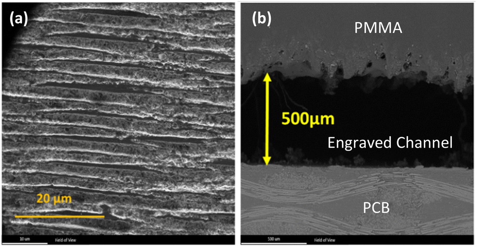 | ||
| Fig. 1 The SEM images of (a) morphology of the microfluidic channel, (b) channel cross section. The scale of the micrographs is different. | ||
2.2 Device fabrication
The general structure of the fabricated microfluidic devices is depicted in Fig. 2(a). The device consists of a microchannel made on PMMA that is sealed by PCB and integrated with a miniature gas sensor. The device fabrication process is presented in Fig. 2(b). First, a microchannel with rectangular cross-section was engraved on PMMA using laser ablation by a conventional 120 W CO2 laser machine. The depth, width and length of the channel was 0.5 mm, 5 mm and 25 mm respectively. After channel formation, PMMA residues were wiped by dry air and the channel was cleaned by deionized water. Then, bonding area patterns and electronic component pads were designed and implemented on PCB. In the next step, PMMA and PCB were bonded together by exposing the interface surfaces to solvent at room temperature and then applying moderate pressure. Finally, the gas sensor was mounted on a small PCB and then installed and soldered on the lid PCB. Prior to sensors installation, the sealed micro-channel was exposed to clean air for degassing in order to reduce the risk of sensor poisoning.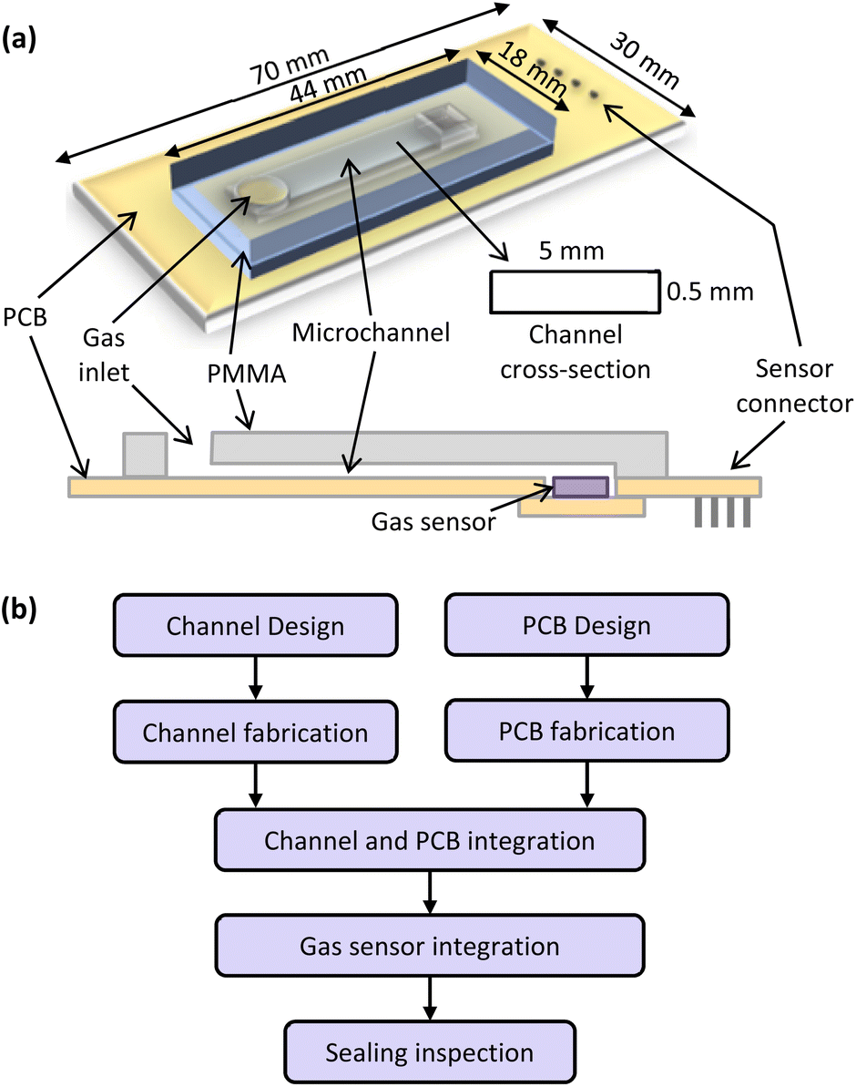 | ||
| Fig. 2 Schematic design of microfluidic-based gas analyzer (a) and fabrication process of the proposed microfluidic-based PCB-PMMA gas analyser (b). | ||
2.3 Sealing test
To ensure the sealing of the fabricated devices, two tests were carried on. In the first sealing test, drops of colored deionized water was applied around the bonded area both outside and inside the channel. The pass criterion was to see no colored liquid in the bonding area. In the second sealing test, the inlet of the device was closed with a piece of thick silicon rubber and then the device was exposed to high concentration of ethanol vapor. Gas sensor response was monitored to detect any gas leakage from outside into the channel. This time, pass criterion was to see negligible response shifts after gas exposure. Typical results of sealing tests are presented in Section 4.2.4 Adhesion strength test
To compare the efficiency of different bonding methods, the strength of PMMA adhesion to PCB was measured using a simple method. For a number of sample prototypes the lid PCB was fixed on a holder and the center of PMMA was pulled with a measurable force. The force was increased until the PMMA was detached from PCB. The maximum force before detachment was recorded as the adhesion strength of the bonding method.2.5 Experimental setup
The schematic diagram of the experimental setup is depicted in Fig. 3. An eight-liter chamber was used to prepare the target gas and a custom data acquisition board was used to measure the sensor response. The specified concentration of analyte was prepared by evaporating a fixed volume of volatile liquid inside the gas chamber. At the beginning of each experiment, the baseline of the gas sensor was recorded for 30 s with a rate of 10 samples per second. Then the inlet of microchannel was aligned with a small hole on the gas chamber to start the gas exposure phase. Transient response of the gas sensor that was proportional to gas concentration at the end of the channel was recorded for 30 s. Then the device was exposed to the clean air to start the recovery phase. Again, the transient response of the sensor was recorded for at least 140 s. This procedure was repeated for different target gases, concentrations and devices and a set of sensor responses was collected for further analysis. All experiments were conducted at room temperature.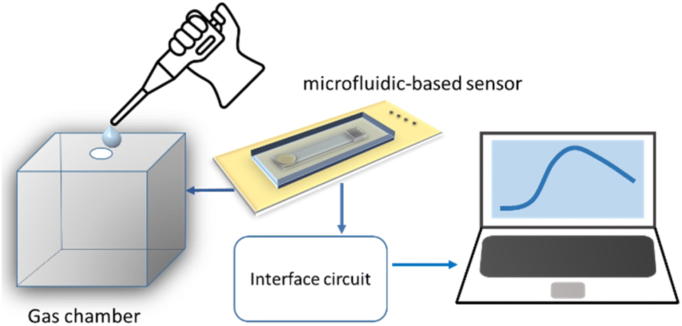 | ||
| Fig. 3 Schematic diagram of the experimental setup. | ||
3. PMMA-PCB bonding
3.1 Bonding process
Here, to develop a reliable bonding process, four affecting parameters including solvent, interface pattern, temperature and pressure were investigated experimentally. As presented in Table 1, eight different bonding processes were planned and carried out. A qualitative measure of the bonding processes is also given in Table 1 for better comparison. In process P1 the effect of solvent on PMMA bonding to the PCB fibre was investigated. Analytical grade chloroform, ethanol and acetone were used as solvents. While the result was better for chloroform, the overall bonding quality was not good. Process P2 was the same as P1 but with smaller or larger bonding area. Neither the smaller area nor the larger one could improve the result of process P1. In process P3, chloroform was applied to interface surface as the solvent and then PMMA was pressed to PCB fiber using a bench vice. The result was worse compared to P1. None of the three investigated processes could yield the desired bonding quality. It can be concluded that the bonding of PMMA to PCB is challenging in terms of adhesion and sealing. So, the copper layer of PCB was used as the interface material in the succeeding processes.| Process parameter | PCB interface material | Adhesion & sealing | ||||||
|---|---|---|---|---|---|---|---|---|
| T | P | S | A | Fiber | Cu | Patterned Cu | ||
| P1 | ● | ● | Bad | |||||
| P2 | ● | ● | ● | Bad | ||||
| P3 | ● | ● | ● | Very bad | ||||
| P4 | ● | ● | Very bad | |||||
| P5 | ● | ● | ● | Very bad | ||||
| P6 | ● | ● | ● | Bad | ||||
| P7 | ● | ● | ● | Very bad | ||||
| P8 | ● | ● | Good | |||||
In process P4, a plain copper similar to the bonding area of PMMA was implemented on PCB. Then chloroform was used as the solvent between copper and PMMA. Contrary to expectations, the resulted bonding was worse compared to P1. In another attempt for bonding improvement, the effect of interface heating was investigated in process P5. In P5, PMMA was pressed to PCB and the copper interface was heated up with electrical current. The bonding quality was not improved compared to P4. Based on the results of P4 and P5 it was concluded that plain copper is not a good interface for bonding to PMMA. Thus, in the third step of bonding investigation, patterned copper on PCB was used as the interface layer. Process P6 was the same as P5 except that patterned Copper was used instead of plain copper. The result was better than P5 but not so good as expected. In process P7 the combined effect of solvent and heating was investigated for patterned copper interface. The bonding quality was not improved compared to P6. In process P8 solvent assisted bonding of patterned copper to PMMA was investigated at room temperature. The bonding quality of P8 was as good as required for fabricating a microfluidic-based gas analyser.
To further improve the efficiency of P8, three different copper patterns were investigated. As depicted in Fig. 4, parallel horizontal copper lines, concentric rectangular copper rings and hexagonal copper mesh were implemented in the boding area. Then PMMA was attached to patterned PCB using chloroform as the solvent. Among the three fabricated samples, concentric rectangular copper rings (Fig. 4(d)) showed the most satisfying result. As a justification for the successful result of process P8 it can be noted that in solvent assisted bonding methods, solvent retention and uniform solvent distribution before solvent evaporation have great impact on bonding quality.32 In the case of patterned copper, especially parallel copper lines, the space between copper lines acts as microchannels that facilitates solvent distribution in the bonding area. Also, the etched space between copper lines acts as a reservoir for solvent retention and hence slower solvent evaporation, a process that can enhance the bonding strength notably at the device edge.42 Also, copper lines act as mechanical barrier against reflow of the solvated PMMA.40
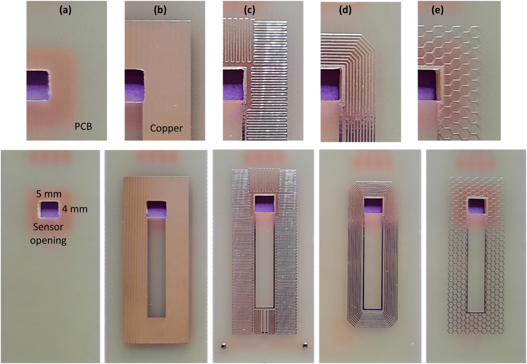 | ||
| Fig. 4 Different surface area patterns on the PCB, (a) no copper layer, (b) plain copper layer, (c) parallel horizontal copper lines, (d) concentric rectangular copper rings, (e) hexagonal copper mesh. | ||
As the final conclusion, based on various investigations on the affecting parameters, the best method for bonding PMMA and PCB was derived with following conditions: the solvent is analytical grade chloroform; the interface is concentric rectangular copper rings on the PCB; the pressure is moderate and applied by hand; the device is made at room temperature.
In addition to copper pattern shape, process P8 can be fine-tuned using the following considerations. The amount of chloroform used must be about 0.5 mL for 44 mm × 18 mm piece of PMMA (0.063 mL per cm squared). The chloroform must be injected/poured gently all over the bonding area. All of the bonding area must be covered with concentric rectangular copper rings (designed on PCB and adapted to the channel shape). The line width of the smallest ring should be more than other rings to perform as a good barrier and prevent chloroform not to enter the channel. In cases where the shape of microfluidic channel is not straight, e.g. the serpentine channel, not only the margin around the microchannel should be covered by patterned copper, but also all of the PMMA area is better to be used for bonding.
3.2 Adhesion and sealing test
The result of sealing test using colored liquid is depicted in Fig. 5 for the best fabricated device (process P8). The test procedure is described in Section 2.3. As can be seen in Fig. 5(a) and (b) no liquid penetration was seen in the bonding area which means the device is perfectly sealed against liquids. Gas phase sealing test was carried out according to the procedure of Section 2.3. The temporal response of the gas sensor during the test is presented in Fig. 6. In zone 1 gas inlet is open and the device is exposed to clean air. In zone 2 the inlet is closed and the response is monitored until the sensor reaches to a stable state. At the onset of zone 3 the device with closed inlet is exposed to a high concentration of ethanol vapor. Then, after around 100 seconds the inlet of microchannel is opened (zone 4). Based on the results, negligible gas penetration is observed. The remarkable change in sensor response after removal of silicon rubber approves good sealing to the gases. | ||
| Fig. 5 Sealing test for the liquid phase using colored liquid for prototype made with process P8: (a) liquid is poured just all around the bonding area and no penetration is seen, (b) liquid is also poured inside the channel to examine no liquid penetrates from the channel into the bonding area, (c) complete view when liquid is poured around the bonding area and inside the channel and no penetration is observed. | ||
 | ||
| Fig. 6 Result of sealing test for gas phase for prototype made with process 8. In zone 1 inlet is open and the device is exposed to air. In zone 2 inlet closed. In zone 3 inlet is closed and the device is exposed to high concentration of ethanol vapor. In zone 4 inlet is opened. | ||
Using the adhesion strength test of Section 2.4, the maximum tolerable force was recorded as the adhesion strength of the bonding for a–d samples of Fig. 5. The result is summarized in Table 2 and as it can be seen, the last method having concentric rectangular copper rings showed the best result for adhesion.
| Type | (a) | (b) | (c) | (d) |
|---|---|---|---|---|
| Pressure (kPa) | 82.1 | 12.7 | 53.2 | 138.9 |
4. Example prototypes
After successful development of the PMMA-PCB bonding process, five different sample prototypes were designed and fabricated to practically assess the combined advantages of PMMA and PCB. These prototypes include fabrication of a simple microfluidic device using a straight PMMA channel, fabrication of a device with serpentine channel, fabrication of a device with two sensors and two channels, using copper tracks on PCB as the channel heater and using SMD resistor for liquid sample evaporation.4.1 Prototype 1: straight channel
The first fabricated prototype contains a straight microfluidic channel with the length, width and depth of 25 mm, 5 mm and 500 μm (Fig. 7(a)). The device was fabricated to investigate the performance of a PCB-PMMA gas detector. In a series of experiments the transient responses of the fabricated device to different concentrations of methanol and ethanol vapours were recorded. At first the device was exposed to clean air for 30 seconds. Then it was exposed to target gas for 30 seconds. Later, the device was exposed to clean air for 140 seconds. The recorded transient responses are presented in Fig. 7(b). Experimental results show that the responses of the PCB-PMMA device are similar to previously reported devices made with other materials. That is, the micro-channel can specifically modulate the gas flow and so forth the sensor response. The results obtained by prototype 1 is a proof of concept for the presented fabrication method.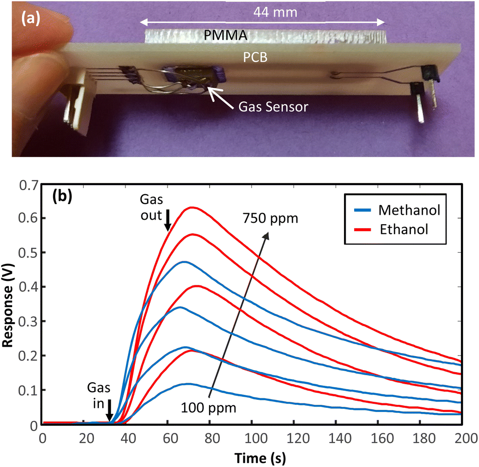 | ||
| Fig. 7 (a) 3D view of the fabricated prototype 1, (b) responses for prototype 1 for various concentrations of methanol and ethanol. | ||
4.2 Prototype 2: serpentine channel
The second prototype is a microfluidic device with serpentine channel. The serpentine channel provides longer path for analytes diffusion in a smaller area. As it is seen in Fig. 8(a)–(d), for good sealing and adhesion, concentric rectangular copper rings were implemented all around the microfluidic channel. The depth of channel was equal to prototype 1. Example responses of the device are presented in Fig. 8(e).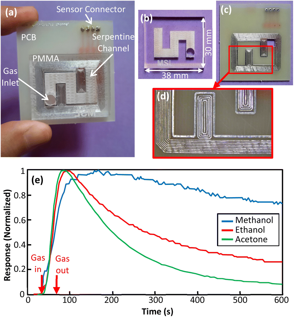 | ||
| Fig. 8 (a) Fabricated prototype 2, (b) engraved serpentine channel on PMMA, (c) PCB lid, (d) zoomed view of copper pattern on PCB, (e) normalized responses for prototype 2 to 500 ppm of acetone, methanol and ethanol vapors. | ||
It can be seen that this structure can distinguish between methanol and ethanol really well as their normalized responses are clearly distinct. Prototype 2 showed that the presented fabrication method can be employed for implementation of devices with non-straight channels.
4.3 Prototype 3: sensor array
One of the advantages of the presented fabrication method is that channels with different dimensions and sensors of different types can be implemented on PMMA and PCB. Then, an array of these devices can be bonded in a single run. To examine the idea, prototype 3 was fabricated (Fig. 9(a) and (b)). In this prototype, the structure includes two different channels with the same length and width, but different depths. Both channels share the same gas inlet. Although the structure is more complex than previous structures, the presented fabrication method could be easily adjusted and concentric rectangular copper rings on the PCB yielded satisfactory adhesion. An array of channels can provide more discriminative information for gas analysis. A reference to sample responses is shown in Fig. 9(c).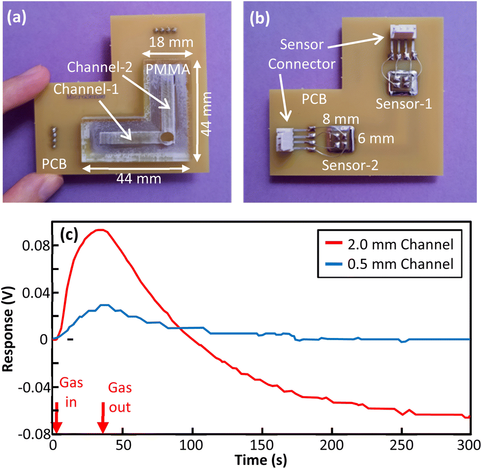 | ||
| Fig. 9 (a) Fabricated prototype 3 top view, (b) fabricated prototype 3 bottom view, (c) responses of prototype 3 to 750 ppm of methanol vapor for two channel depths. | ||
4.4 Prototype 4: copper track as channel heater
In the presented fabrication method, PCB is used for channel cap. So, copper layer on PCB can be utilized as one of the channel walls. Patterns can be implemented on copper to affect the gas flow inside the channels. Also, tracks of copper can be used as a micro heater for temperature regulation. In prototype 4 a serpentine track of copper was implemented in channel area as a microheater (Fig. 10(a)). The ability of this microheater in modulating channel temperature and hence gas flow was examined. As presented in Fig. 10(b), a series of voltage pulses was applied to the microheater after gas exposure for minute. From the recorded transient response, the effect of temperature modulation on gas flow is remarkable. This method is likely a good approach for obtaining more discriminative transient responses for gas analysis. | ||
| Fig. 10 (a) Fabricated prototype 4 with copper track as channel heater, (b) normalized responses for prototype 4 for 250 ppm of methanol and ethanol when 1 min of pulsed temperature modulation is applied. | ||
4.5 Prototype 5: SMD resistor as liquid evaporator
Utilizing PCB for device fabrication enables simple integration of electronic components with micro channel. In prototype 5 an SMD resistor was mounted at channel inlet for thermal evaporation of liquid samples (Fig. 11(a)). The SMD resistor was heated by applying a voltage and then a specified amount of methanol and ethanol was poured on it with the help of a micropipette. In Fig. 11(b), the recorded transient responses have been compared with those recorded for gas samples. It is shown that using prototype 5 the need for gas chamber is eliminated and faster responses are obtained. Following this approach, an array of SMD resistors can be mounted inside the channel for temperature modulation. Also, other miniature electronic components can be used for special purposes. | ||
| Fig. 11 (a) Fabricated prototype 5, (b) normalized responses for prototype 5 for 1.2 μL of methanol and ethanol compared to normalized responses for prototype 1 for 100 ppm of methanol and ethanol. | ||
5. Conclusions
In this study we proposed a novel method for rapid prototyping of microfluidic-based gas analysers using PMMA and PCB. It was shown that patterned interface of concentric rectangular copper rings exposed to solvent at room temperature and under moderate pressure provides reliable bonding and good sealing between PCB and PMMA. Also, it was shown that gas sensor can be installed and soldered after channel bonding to prevent sensor poisoning. Five different prototypes were fabricated and tested to examine different aspects of the proposed fabrication method. It was shown that the method can yield good bonding for non-straight channels. Moreover, it makes the implementation of array of sensors in a single fabrication run possible. Utilizing copper tracks on PCB as microheater for flow modulation was another feature that could be added to the device by this method. As an example of integration of electronic components with micro channel, one prototype for liquid sample evaporation was demonstrated. Using the proposed device fabrication method, microfluidic channels with complex patterns can be implemented on a single PMMA substrate. Moreover, gas sensor along with other electronic components including the microprocessor can be implemented on a single PCB and then channel and electronic integration can be done in a single bonding run.Data availability
All of the experimental data have been presented in the article. No external data or code from other sources has been used in this article.Conflicts of interest
There are no conflicts to declare.References
- G. Roberdao, S. I. C. J. Palma and A. C. A. Roque, Sensors, 2020, 20, 5742 CrossRef.
- S. Kaaliveetil, J. Yang, S. Alssaidy, Z. Li, Y.-H. Cheng and N. H. Menon, et al., Micromachines, 2022, 13, 1716 CrossRef PubMed.
- A. Yeganegi, K. Yazdani, N. Tasnim, S. Fardindoost and M. Hoorfar, Front. Chem., 2023, 11, 1267187 CrossRef CAS PubMed.
- V. Ghafarinia, A. Amini and M. Paknahad, Sens. Lett., 2012, 10, 1–5 CrossRef.
- F. Hossein-Babaei, M. Paknahad and V. Ghafarinia, Lab Chip, 2012, 12, 1874 RSC.
- L. Zhu, D. Meier, Z. Boger, C. Montgomery, S. Semancik and D. L. DeVoe, Sens. Actuators, B, 2007, 121, 679–688 CrossRef CAS.
- S. Zampolli, I. Elmi, J. Sturmann, S. Nicoletti, L. Dori and G. C. Cardinali, Sens. Actuators, B, 2005, 105, 400–406 CrossRef CAS.
- M. Paknahad, J. S. Bachhal, A. Ahmadi and M. Hoorfar, Sens. Actuators, B, 2017, 241, 55–64 CrossRef CAS.
- M. T. Aly, N. Tasnim, H. Najjaran, S. Fardindoost and M. Hoorfar, Sens. Actuators, B, 2024, 403, 135201 CrossRef CAS.
- S. Janfaza, E. Kim, A. O'Brien, H. Najjaran, M. Nikkhah, T. Alizadeh and M. Hoorfar, Sci. Rep., 2019, 9, 19051 CrossRef CAS.
- M. Ghazi, S. Janfaza, H. Tahmooressi, A. Ravishankara, E. Earl and N. Tasnim, et al., Sens. Actuators, B, 2021, 342, 130050 CrossRef CAS.
- M. Ghazi, S. Janfaza, H. Tahmooressi, N. Tasnim and M. Hoorfar, J. Hazard. Mater., 2022, 424, 127566 CrossRef CAS PubMed.
- F. Hossein-Babaei and V. Ghafarinia, Anal. Chem., 2010, 82, 8349–8355 CrossRef CAS.
- M. Paknahad, V. Ghafarinia and F. Hossein-Babaei, IEEE Sensors Application Symposium, Brescia, Italy, 2012 Search PubMed.
- F. Hossein-Babaei, A. H. Zare and M. Gharesi, Anal. Chem., 2019, 91, 12827–12834 CrossRef CAS.
- M. Aghaseyedi, A. Salehi, S. Valijam and M. Shooshtari, Micromachines, 2022, 13, 1504 CrossRef.
- M. Kim, H. Alrowais, C. Kim, P. Yeon, M. Ghovanloo and O. Brand, Lab Chip, 2017, 17, 2323–2329 RSC.
- A. P. Vollmer, R. F. Probstein, R. Gilbert and T. Thorsen, Lab Chip, 2005, 5, 1059–1066 RSC.
- V. Martini, S. Bernardini, M. Bendahan, K. Aguir, P. Perrier and I. Graur, Sens. Actuators, B, 2012, 170, 45–50 CrossRef CAS.
- V. Martini-Laithier, I. Graur, S. Bernardini, K. Aguir, P. Perrier and M. Bendahan, Sens. Actuators, B, 2014, 192, 714–719 CrossRef CAS.
- Y. Ueno, T. Horiuchi, T. Morimoto and O. Niwa, Anal. Chem., 2001, 73, 4688–4693 CrossRef CAS PubMed.
- S. H. Lee, E. H. Oh and T. H. Park, Biosens. Bioelectron., 2015, 74, 554–561 CrossRef CAS PubMed.
- D. Yang, K. Kang, D. Kim, Z. Li and I. Park, Sci. Rep., 2015, 5, 8149 CrossRef PubMed.
- F. Perdigones, Micromachines, 2021, 12, 175 CrossRef.
- F. Perdigones and J. M. Quero, Micromachines, 2022, 13, 460 CrossRef.
- D. Moschou and A. Tserepib, Lab Chip, 2017, 17, 1388 RSC.
- C. Yong-Jia and Y. Hu, Chin. J. Anal. Chem., 2019, 47, 965–975 Search PubMed.
- E.-H. Lee, S. G. Lee, B. H. O, S. G. Park, K. H. Kim and J. K. Kang, et al., Proc. SPIE, 2005, 5724, 112–123 CrossRef CAS.
- W. Zhao, S. Tian, L. Huang, K. Liu and L. Dong, Electrophoresis, 2020, 41, 1433–1445 CrossRef CAS.
- H. Shamkhalichenar, C. J. Bueche and J.-W. Choi, Biosensors, 2020, 10, 159 CrossRef CAS PubMed.
- N. R. Ali@Hasim, A. Ahaitouf and M. Z. Abdullah, Meas. Sci. Technol., 2021, 32, 052001 CrossRef.
- K. Giri and C.-W. Tsao, Micromachines, 2022, 13, 486 CrossRef PubMed.
- D. Moschou, T. Trantidou, A. Regoutz, D. Carta, H. Morgan and T. Prodromakis, Sensors, 2015, 15, 18102–18113 CrossRef CAS PubMed.
- D. Moschou, L. Greathead, P. Pantelidis, P. Kelleher, H. Morgan and T. Prodromakis, Biosens. Bioelectron., 2016, 86, 805–810 CrossRef CAS PubMed.
- B. Salvador, E. Franco, F. Perdigones and J. M. Quero, Microelectron. Eng., 2017, 173, 6–12 CrossRef CAS.
- F. Perdigones, E. Franco, B. Salvador, G. Flores and J. M. Quero, J. Electromech. Syst., 2018, 27, 479–486 CAS.
- D. Evans, K. I. Papadimitriou, N. Vasilakis, P. Pantelidis, P. Kelleher and H. Morgan, et al., Sensors, 2018, 18, 4011 CrossRef.
- Y. Chang and H. You, Anal. Methods, 2019, 11, 1229–1236 RSC.
- J. D. Urbano-Gamez, L. Valdes-Sanchez, C. Aracil, B. de la Cerda, F. Perdigones and A. P. Reyes, et al., Micromachines, 2021, 12, 1469 CrossRef PubMed.
- E. Franco, B. Salvador, F. Perdigones, M. Cabello and J. M. Quero, Microelectron. Eng., 2018, 194, 31–39 CrossRef CAS.
- F. Perdigones and J. M. Quero, Sens. Actuators, A, 2019, 300, 111639 CrossRef CAS.
- A. M. D. Wan, A. Sadri and E. W. K. Young, Lab Chip, 2015, 15, 3785–3792 RSC.
| This journal is © The Royal Society of Chemistry 2024 |