DOI:
10.1039/D4RA02652G
(Paper)
RSC Adv., 2024,
14, 18567-18575
Post-hot-cast annealing deposition of perovskite films with infused multifunctional organic molecules to enhance the performance of large-area light-emitting devices†
Received
9th April 2024
, Accepted 28th May 2024
First published on 10th June 2024
Abstract
All-inorganic perovskites show great promise as an emission layer in perovskite light-emitting diodes (PeLEDs) owing to their easy solution processing, low manufacturing cost, and excellent optoelectronic properties. However, there is still an immense performance gap from small-area devices to large-area PeLED devices. The inhomogeneity of large-area high-quality perovskite films inevitably leads to vast defects and electroluminescence performance losses. Herein, a post-hot-cast annealing deposition scheme and the introduction of the multifunctional molecule 2-amino-1,3-propanediol (APDO) were proposed to regulate the crystallization of the perovskite film. As a result, uniform APDO:CsPbBr2.5Cl0.5 perovskite films with high crystallinity and lower defect density were deposited by post-hot-cast annealing. A decent maximum brightness of 2659 cd m−2 was achieved for the large-area cyan PeLEDs with an emitting area of 400 mm2.
1. Introduction
Metal halide perovskite (MHP) materials have many advantages such as wide color gamut, high luminous efficiency, and low synthesis cost.1–4 Since the first room-temperature emitting perovskite light-emitting diode (PeLED) was reported in 2014,5 various performance parameters of PeLEDs have rapidly improved in a few years. The external quantum efficiency (EQE) of green, red and near-infrared emitting PeLEDs has exceeded 20%,6–8 and the blue PeLEDs achieved a record of 18.6%.9 Several scientific research groups have recently reported PeLEDs with lifetimes exceeding 10![[thin space (1/6-em)]](https://www.rsc.org/images/entities/char_2009.gif) 000 hours,10 demonstrating the feasibility of overcoming the intrinsic instability of perovskite materials. Performance indicators of PeLEDs continue to approach the most advanced organic and quantum dot LEDs, and they exhibit unique advantages in terms of color purity, material cost, etc. Therefore, PeLEDs stand out in the field of wide color gamut display and have drawn much interest from both academia and industry.11–14 Despite the impressive progress, PeLEDs still face some challenges in achieving commercial display applications. On the one hand, high-performance PeLEDs only work in a small active layer area. The high degree of inhomogeneity of large-area films becomes a major obstacle when the active layer area expands.15–17 On the other hand, most studies on PeLEDs focus on prototype devices with a single emitting pixel. High-resolution, full-color MHP array patterning strategies and device integration technology are relatively lagging behind, which strongly hinders the commercialization of PeLED displays. In addition, high-performance PeLEDs are mainly prepared based on rigid substrates, thus limiting their potential application scenarios.
000 hours,10 demonstrating the feasibility of overcoming the intrinsic instability of perovskite materials. Performance indicators of PeLEDs continue to approach the most advanced organic and quantum dot LEDs, and they exhibit unique advantages in terms of color purity, material cost, etc. Therefore, PeLEDs stand out in the field of wide color gamut display and have drawn much interest from both academia and industry.11–14 Despite the impressive progress, PeLEDs still face some challenges in achieving commercial display applications. On the one hand, high-performance PeLEDs only work in a small active layer area. The high degree of inhomogeneity of large-area films becomes a major obstacle when the active layer area expands.15–17 On the other hand, most studies on PeLEDs focus on prototype devices with a single emitting pixel. High-resolution, full-color MHP array patterning strategies and device integration technology are relatively lagging behind, which strongly hinders the commercialization of PeLED displays. In addition, high-performance PeLEDs are mainly prepared based on rigid substrates, thus limiting their potential application scenarios.
At present, as the device area increases the performance decreases even more. When large-area perovskite films are prepared, due to the limitations of solution processing and interface preparation processes, the uniformity of the perovskite film deteriorates, pores increase, and defects increase. The development of feasible large-area MHP thin film deposition technology is necessary to realize large areas of PeLED devices. It has been reported that the preparation methods of large-area perovskite films include blade coating,18,19 slot-die coating,20,21 spray coating,22,23 inkjet printing,24 and vapor deposition.25,26 So far, benefiting from the improvement of MHP film quality and the optimization of device structures, large-area PeLEDs have made some important breakthroughs. For example, large-area PeLEDs have achieved an EQE of more than 16% and a light-emitting area of more than 40 cm2.17,25,27,28 Despite this, the performance of large-area PeLEDs is generally inferior to that of small-area PeLEDs, which is mainly attributed to the difficulty in fabricating defect-free, uniform, dense, and high-quality MHP emissive layers. The resulting pinholes or cracks will increase defect-induced non-radiative recombination and leakage current, thereby reducing PeLED performance and increasing energy consumption.
Nowadays, spin coating (SC) is widely used to prepare perovskite films, and the use of large-area substrates will cause problems with the coffee ring effect and unevenness. It has been reported that the hot-casting (HC) method was used to prepare large-area perovskites. They believe that due to the reduced surface tension between the perovskite precursor solution and the substrate, preheating the substrate with high thermal energy can promote the growth of uniform and large-area perovskite films.29,30 In the current production of PeLEDs, the substrate is hot annealed after spin coating, which accelerates the formation of the perovskite film. However, it is reversed in the hot-casting method. The substrate is preheated first and then spin-coated to form a perovskite film. This makes the growth process of the perovskite crystal advance as a whole, and the growth of the crystal nucleus is completed at the end of the spin-coating stage. In our preliminary experiments, we found that unless the temperature is increased (nearly 200 °C), the perovskite film is not completely crystallized after spin coating, and the surface is still in a solid–liquid mixed state. Therefore, it is necessary to anneal after the process to improve the crystallization quality of perovskite films. At the same time, Shen et al. reported that when the multifunctional organic molecule 2-amino-1,3-propanediol (APDO) is doped into PEDOT:PSS, it triggers the “anchoring effect” at the grain growth interface, which is helpful for the deposition of large-area perovskite films.31 Inspired by this problem, we proposed adding APDO to the perovskite precursor solution in the hope that the incorporation of APDO would make the large-area perovskite solution hydrophilic and make the film more uniform and non-porous. Finally, the large-area cyan APDO:CsPbBr2.5Cl0.5 PeLED (measured at 400 mm2) achieved a maximum EQE of 2.81% and a maximum brightness of 2659 cd m−2, respectively.
2. Experimental section
2.1 Materials
Cesium bromide (CsBr, 99.9%), lead bromide (PbBr2, 98+%), and cesium chloride (CsCl, 99.99%) were purchased from Alfa Aesar. Poly(ethylene oxide) (PEO) and Al ingot (99.997%) were purchased from Sigma-Aldrich. PEDOT:PSS (Clevios Al 4083) was purchased from Heraeus. 1,3,5-Tris(1-phenyl-1H-benzimidazol-2-yl)benzene (TPBi, 99.5%) was purchased from Lumtec. 2-Amino-1,3-propanedio (APDO, 97+%), dimethyl sulfoxide (DMSO, 99.9%), gamma-butyrolactone (GBL, 99.9%), and lithium fluoride (LiF, 99.99%) were purchased from Uni-Onward. Patterned ITO-coated glass substrates with an area of 30 mm × 20 mm with a characteristic of 7 Ω/□ were designed and purchased from Ruilong.
2.2 Preparation of APDO:CsPbBr2.5Cl0.5 perovskite solution
The cyan CsPbBr2.5Cl0.5 perovskite precursor solution was prepared by dissolving CsCl (100.8 mg), CsBr (253.6 mg), and PbBr2 (440.4 mg) in 4 ml of DMSO solvent, in which the concentration was fixed at 0.3 M, followed by stirring at 140 °C for 30 min. The PEO additive (10 mg ml−1 dissolved in DMSO) was incorporated into 4 mg TPBi and blended with the CsPbBr2.5Cl0.5 precursor solution, which was stirred at 25 °C for 4 h. APDO:CsPbBr2.5Cl0.5 perovskite precursor solution with three different doping contents were prepared under these optimized conditions by choosing the APDO infusion contents as 1 mg, 2 mg, and 3 mg. The perovskite films prepared using the traditional spin coating (SC) and hot casting (HC) methods were named SC perovskite and HC perovskite, respectively. According to different APDO doping contents, the corresponding samples were named hereafter as HC-1mg APDO, HC-2mg APDO and HC-3mg APDO, respectively.
2.3 Device fabrication
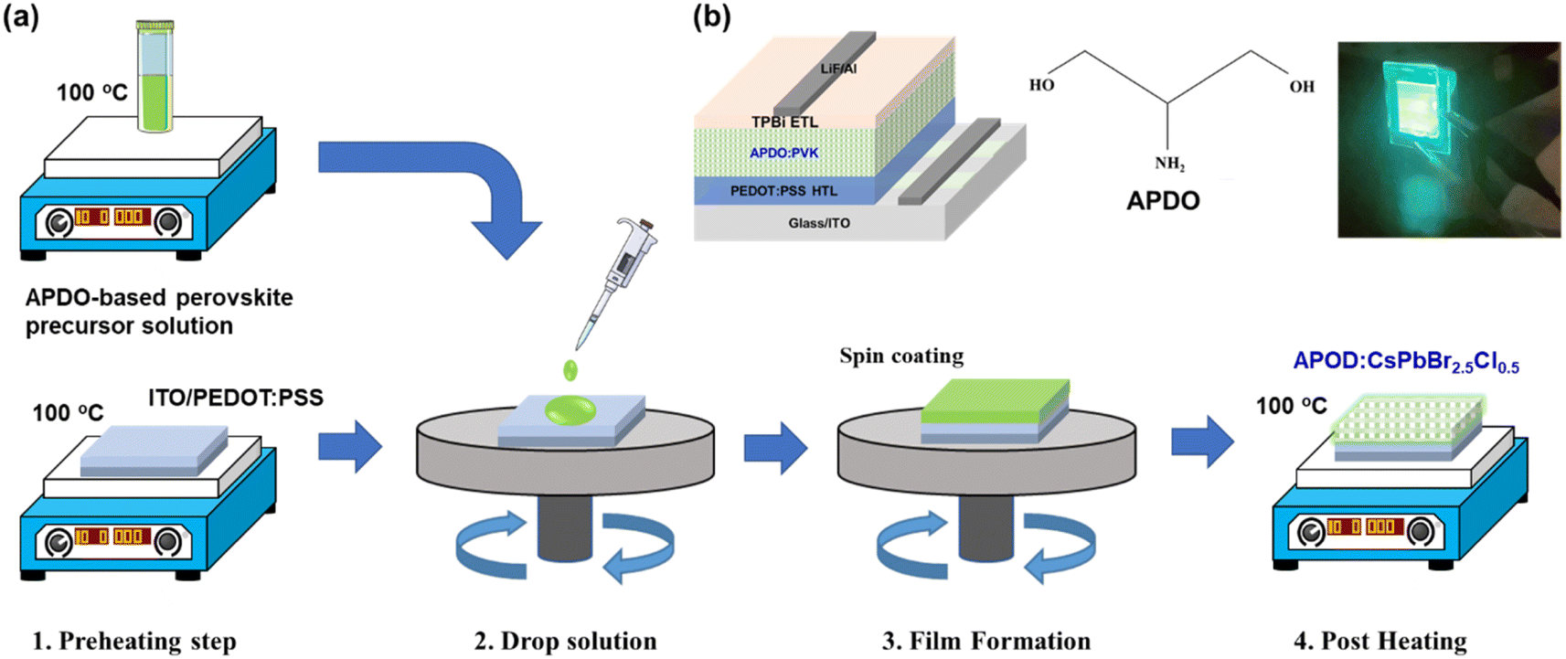
The PEDOT:PSS solution was spin-cast onto a patterned ITO-coated glass substrate at 4500 rpm for 45 s and then annealed for 20 min at 140 °C in air as a hole-transport layer (HTL). The PEDOT:PSS/ITO glass substrate was placed in a N2-filled glove box. Preheating (hot-casting) of the perovskite precursor and HTL substrate was performed at 100 °C for 30 min on a hot plate. Then, the precursor was deposited within 5 s after transferring the substrate to the spin coater. The 160 μL precursor was spin-coated onto HTL substrate at 3000 rpm for 60 s and baked at 100 °C for 10 min (post-heating), as shown in Fig. 1(a). Finally, TPBi (40 nm) electron-transport layer (ETL) and LiF (1 nm)/Al (150 nm) bilayer cathode were deposited on the top of the devices through thermal evaporation under a high vacuum of 5 × 10⁻⁶ torr. The overall APDO:CsPbBr2.5Cl0.5 PeLED structure and luminescence photo are shown in Fig. 1(b). On the other hand, we also use the traditional spin coating (not hot-casting) perovskite films to prepare PeLED devices. All corresponding PeLED devices in this study were named below as SC-PeLED, HC-PeLED, HC-1mg APDO PeLED, HC-2mg APDO PeLED, and HC-3mg APDO PeLED.
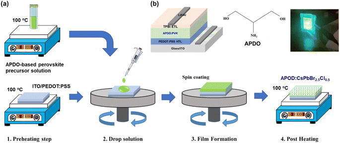 |
| | Fig. 1 (a) Schematic of the synthesis route for APDO:CsPbBr2.5Cl0.5 perovskite films. (b) Schematic device structure of PeCLED and luminescence photo. | |
2.4 Sample characterization
Steady-state photoluminescence (PL) spectra and photoluminescence quantum efficiencies (PLQYs) of the perovskite films were recorded using an integrated spectrometer LQ-100X-PL (Enlitech, Kaohsiung, Taiwan) with a fixed excitation wavelength at 365 nm at room temperature. Time-resolved photoluminescence (TRPL) spectra were measured through an iHR320 imaging spectrometer (Horiba Jobin Yvon, France) with a 375 nm picosecond pulsed laser as an excitation source. X-ray diffraction (XRD) patterns were performed using an X'Pert PRO MRD X-ray diffractometer (XRD, Malvern panalytical, Netherlands) with a Cu X-ray tube (λ = 1.5418 Å) radiation source set to 45 kV and 40 mA. Scanning electron microscopy (SEM) images of perovskite films were obtained using a high-resolution thermal field emission scanning electron microscope (JSM-7610F, JEOL, Japan). The current density–voltage (J–V), luminescence, CE, EQE, and electroluminescence (EL) spectra of the encapsulated devices were collected using a system comprised of PR-670 spectra scan spectroradiometer (Syracuse, NY, USA) coupled with a Keithley 2400 source meter (US, Keithley Instruments).
3. Results and discussion
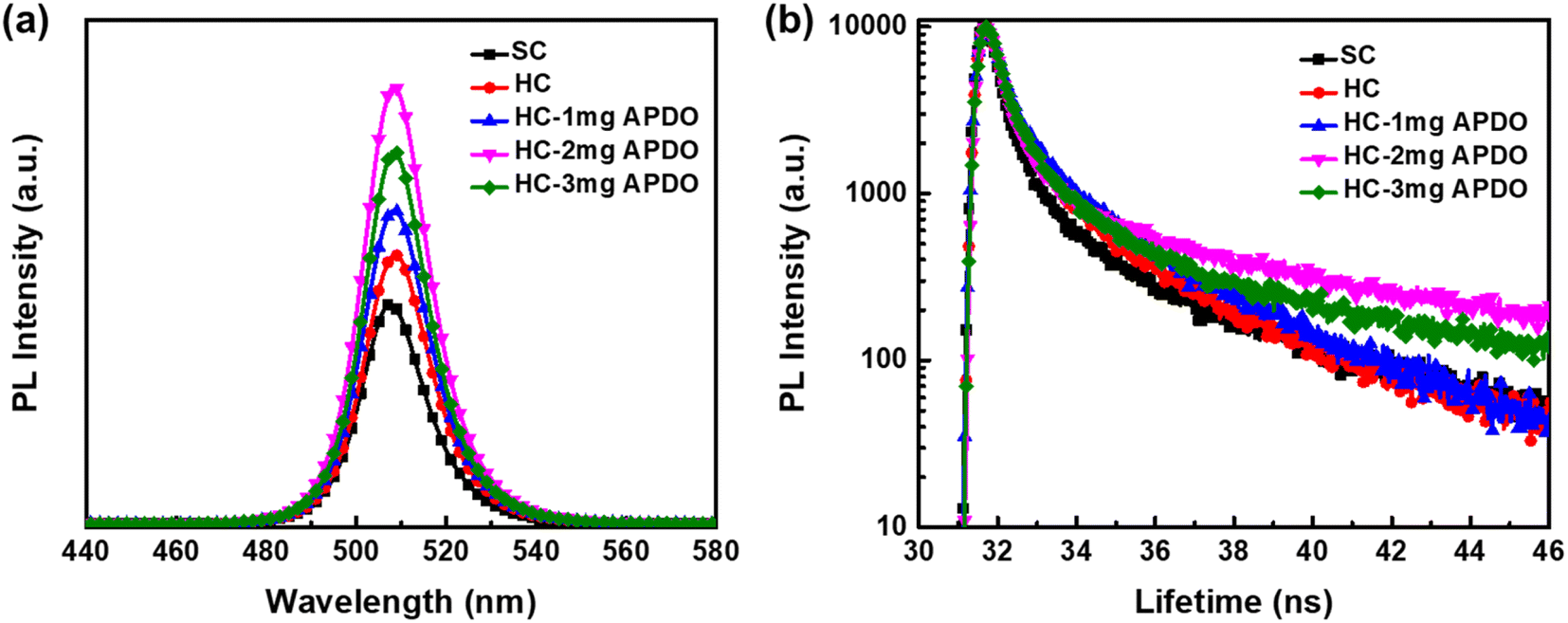
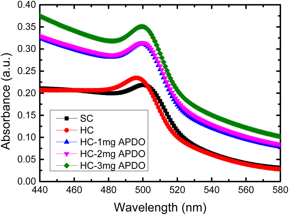
Fig. 2(a) shows the PL spectra of perovskite films prepared by different methods and doped with different contents of APDO. It can be seen that the PL intensity increases significantly when the spin-coating method is replaced by the hot-casting method, and the intensity increases with the proportion of APDO doping. Among them, the HC-2mg APDO perovskite film obtains the highest PL intensity and better PLQY, reaching 14.45%, which is twice as high as the PLQY of the SC perovskite film prepared by spin-coating without APDO. However, the HC-3mg APDO perovskite film may cause lattice distortion due to excessive doping, resulting in a decrease in PL intensity. In addition, the wavelength of the SC perovskite film prepared by spin-coating without APDO was 507 nm, while the wavelength of the HC perovskite film and the HC-APDO perovskite film treated by hot-casting and doping with APDO showed a red shift to 508 nm. Moreover, as the doping content of APDO increased, the wavelength position did not change, indicating that the red-shift of the wavelength was related to the hot-casting method. Next, when the spin-coating method was replaced by the hot-casting method, the FWHM of the SC perovskite film decreased from 19.8 nm to 18.742 nm (HC perovskite film). By doping APDO, the FWHM can be further reduced. The HC-2mg APDO perovskite film has the narrowest FWHM of 18.03 nm, indicating that both the hot-casting method and APDO doping have the effect of reducing defects and improving the crystallization quality of perovskite, thereby increasing the radiative recombination probability of the material. Fig. 2(b) shows the time-resolved PL curves of perovskite films prepared by different methods and doped with different contents of APDO. The decay curves of TRPL were fitted by a bi-exponential function (I(t) = A1exp(−t/τ1) + A2exp(−t/τ2)), and the average decay time of perovskite films was calculated. It can be seen that the hot-casting method significantly improved the carrier lifetime compared to the spin-coating method. The carrier lifetime of the HC-2mg APDO perovskite film reached 1.137 ns, indicating fewer defects in the film and that the excited carriers could emit fluorescence by radiative recombination. This also indicates that the optical properties of the film under this condition were better. Table S1† summarizes the CsPbBr2.5Cl0.5 perovskite films prepared by different methods and doped with different contents of APDO and their PL peak, FWHM, PLQY, and lifetime values. Fig. 3 plots the absorption spectra of CsPbBr2.5Cl0.5 perovskite films with different preparation methods and APDO doping contents. The samples with APDO doping demonstrate better absorption than samples without APDO doping owing to smooth surfaces and less reflection.
 |
| | Fig. 2 (a) Photoluminescence (PL), and (b) time-resolved PL spectra of the CsPbBr2.5Cl0.5 perovskite films with different preparation methods and different APDO doping contents. | |
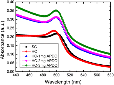 |
| | Fig. 3 Absorption spectra of CsPbBr2.5Cl0.5 perovskite films with different preparation methods and different APDO doping contents. | |
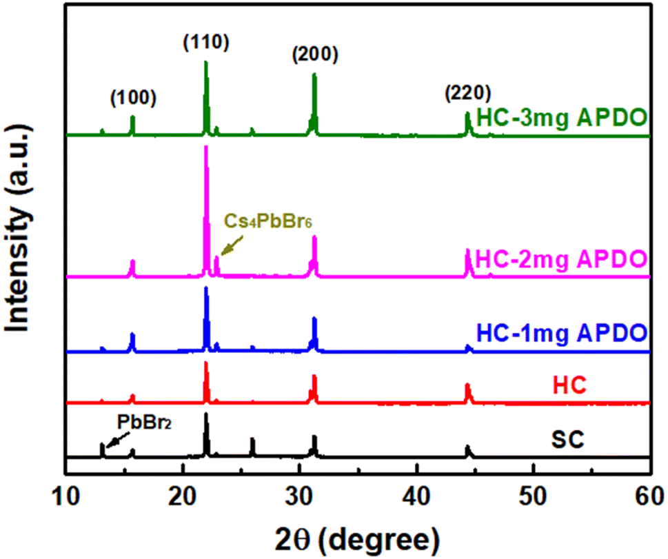
Fig. 4 shows the XRD patterns of perovskite films prepared and doped with different contents of APDO by different methods. Basically, four main diffraction peaks were displayed for each parameter. Due to the incorporation of Cl in the perovskite composition, the XRD diffraction peak angle increases,32 causing the XRD pattern to shift to the right. Therefore, the shifted XRD pattern was between CsPbBr3 and CsPbCl3 and closer to CsPbBr3. Taking the XRD pattern of the orthorhombic crystal of the all-inorganic perovskite CsPbBr3 as an example, diffraction peaks usually appear at about 15°, 21°, 31° and 43°, corresponding to the lattice planes of (100), (110), (200) and (220), respectively.33 The measured diffraction peaks of CsPbBr2.5Cl0.5 moved slightly to larger angles, about 15.7°, 21.9°, 31.25° and 44.35°, proving that some of the chlorine replaced the bromine in the octahedral structure. Because the ionic radius of chlorine is 181 pm, which is smaller than the ionic radius of bromine (196 pm), the bond length between chlorine and lead ions was shortened, resulting in lattice contraction, which leads to the movement towards the direction of increased diffraction angle. To achieve better optoelectronic properties, the ratio of CsBr was increased in the precursor solution. This would result in the formation of Cs4PbBr6,33 which was an intermediate phase before the conversion to CsPbBr3. Cs4PbBr6 has inferior optoelectronic properties than CsPbBr3, but a suitable ratio can improve the overall performance. Therefore, the characteristic peaks of Cs4PbBr6 (ref. 34) were observed at 13.1°, 22.1° and 25.9° in the SC perovskite films prepared by the spin-coating method. When the hot-casting method was used, the intensity of the diffraction peaks increased, indicating the enhancement of crystallinity. The crystallinity was further improved after doping with APDO, showing that HC-2mg APDO perovskite film had a significant increase in crystallinity. In the XRD results, when APDO is added at 2 mg ml−1, the characteristic peak at 22.1° is significantly enhanced, while those at 13.1° and 25.9° are notably weakened. The phenomenon may be attributed to the “anchoring effect” of APDO in the perovskite layer due to the stack of nucleating seeds being tightly linked, with a uniform orientation onto the substrate.31 In addition, the characteristic peaks of Cs4PbBr6 decreased significantly after using the hot-casting method. When the doping content of APDO was 2 mg, all the characteristic peaks except 22.1° disappeared, suggesting that the perovskite had fewer impurities and a more regular lattice structure under this condition.
 |
| | Fig. 4 XRD patterns of CsPbBr2.5Cl0.5 perovskite films with different preparation methods and APDO doping contents. | |
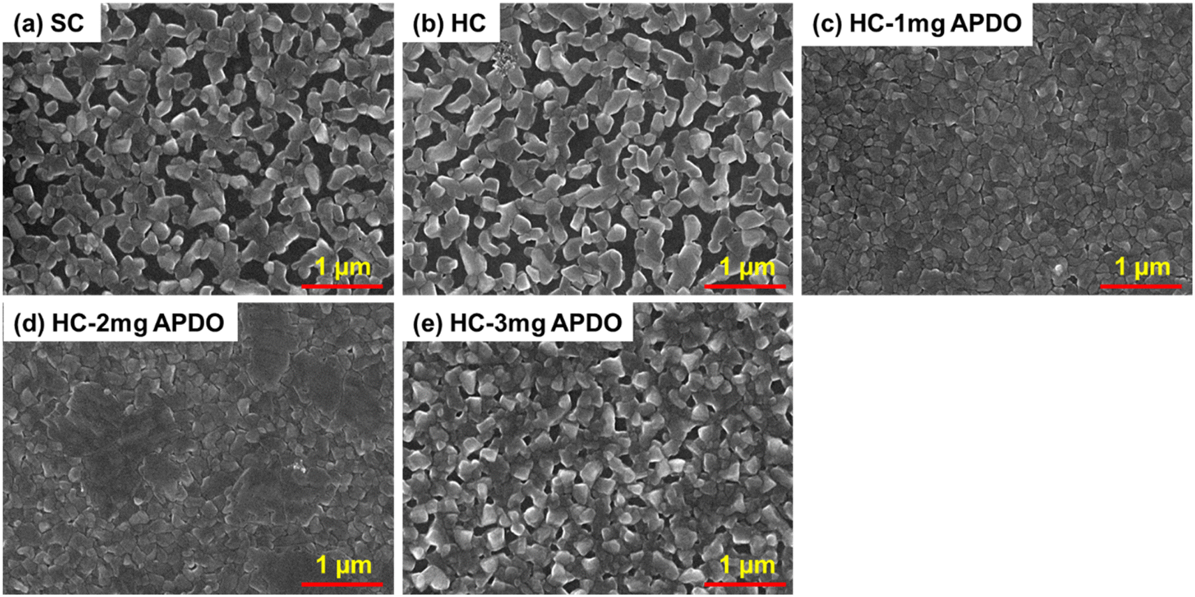
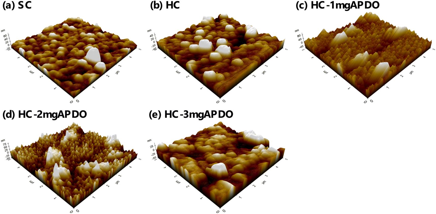
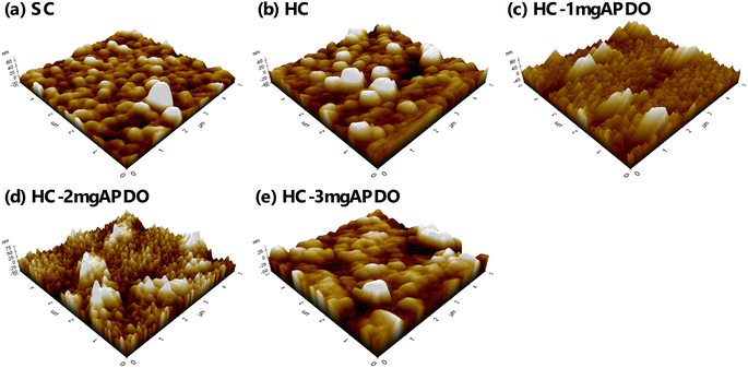
The morphology of perovskite films affects the performance of the LED devices. Too many and too large pores will cause carriers to directly penetrate and undergo non-radiative recombination. The increase in leakage current also increases the current density, reducing the luminous efficiency. Fig. 5 shows the SEM surface morphology of perovskite films prepared by different methods and doped with different contents of APDO. There was not much difference in the morphology of the film growth between the spin-coating (Fig. 5(a)) and the hot-casting methods (Fig. 5(b)). The main difference was the average grain size under the domain size. In the spin-coating method, many small grains can be seen growing together, and different grains can be distinguished by the grain boundary lines. In the hot-casting method, a large number of reduced grain boundaries can be observed, indicating that the grains were annealed for a longer time by the hot-casting method, thereby eliminating the grain boundaries and synthesizing a larger crystal. Larger grains tend to perform better in optoelectronic properties and lifetime. Fig. 5(c–e) show the improvement of the CsPbBr2.5Cl0.5 morphology by doping APDO. When 1 mg of APDO was doped, the small molecules of APDO could better assist in repairing defects, significantly reducing pores. The overall domain size was composed of many small grains that were joined together to form a dense plane, which initially suppressed the generation of leakage current and better confined the probability of radiative recombination. When 2 mg of APDO was doped, the amount of APDO doping reached the optimal parameter, and large grains appeared in large quantities and further reduced defects, resulting in a denser and smoother surface morphology. When 3 mg of APDO was doped, the surface stacking was obvious, forming a large number of small hills, and pores appeared in the film, which was attributed to the excessive addition of APDO, which caused the growth to be worse than expected. Fig. 6 shows the AFM (atomic force microscopy) pictures of CsPbBr2.5Cl0.5 perovskite films with different preparation methods and APDO doping contents. Their root mean square deviation values are 31.5, 24.2, 20.6, 18.2, and 26.6 nm, corresponding to SC (Fig. 6(a)), HC (Fig. 6(b)), HC-1mg APDO (Fig. 6(c)), HC-2mg APDO (Fig. 6(d)), and HC-3mg APDO (Fig. 6(e)), respectively. The results are consistent with the SEM images. The APDO doping can improve the morphology of perovskite films.
 |
| | Fig. 5 Surface SEM images of CsPbBr2.5Cl0.5 perovskite films with different preparation methods and APDO doping contents. | |
 |
| | Fig. 6 AFM images of CsPbBr2.5Cl0.5 perovskite films with different preparation methods and APDO doping contents. | |
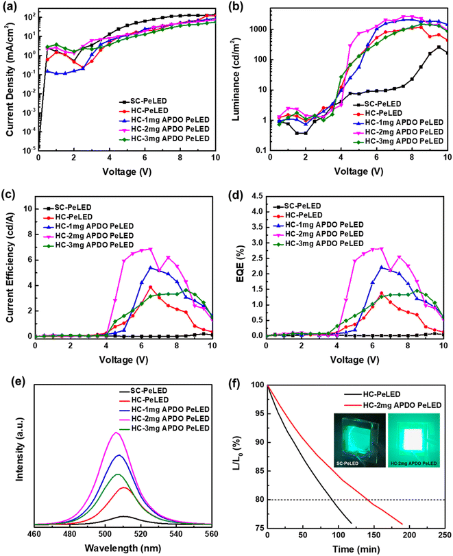
The J–V characteristics of large-area PeLEDs are shown in Fig. 7(a). The current densities of all PeLEDs start increasing in the range of 2.5–3.0 V. The current density curve of the SC-LED rises the fastest, which was caused by the leakage current generated by slightly more surface defects. After changing to the hot-casting method, the current density curve rises more slowly, indicating that fewer surface defects limit the leakage current. When doped with APDO, the current density becomes more gentle, and the current density is lower than 100 mA cm−2. The optoelectronic performance of CsPbBr2.5Cl0.5 PeLEDs with different preparation methods and APDO doping contents are summarized in Table S2.† Fig. 7(b) shows the luminance–voltage characteristics of the large-area PeLEDs. The SC-PeLED prepared by the spin-coating method has a low overall luminance, with a maximum luminance of 263 cd m−2 and a turn-on voltage of 3 V (>1 cd m−2). The HC-PeLED prepared by the hot-casting method has a turn-on voltage of about 2.5 V and a maximum luminance of more than 1000 cd m−2. As the doping contents of APDO increases, the maximum luminance of the device gradually increases. When the doping content of APDO was 2 mg, the HC-2mg APDO PeLED device has a maximum luminance of 2659 cd m−2 at 7.5 V. When the doping content of APDO increases to 3 mg, the excess small molecules cause distortion of the perovskite CsPbBr2.5Cl0.5 grains, which indirectly increases the surface defects and reduces the overall luminance of the device. The CE–V characteristics curve is shown in Fig. 7(c). The SC-PeLED only showed current efficiency at about 8 V, while the PeLEDs prepared by the hot-casting method started at about 3.5–4 V. The current efficiency increased with the increase in APDO doping contents, and the HC-2mg APDO PeLED achieved the highest current efficiency of 6.86 cd A−1, which was related to its dense and large-grained surface morphology. The HC-3mg APDO PeLED had a lower current density because the excessive doping of APDO resulted in poor surface morphology, which could not create good radiative recombination for carriers. Fig. 7(d) shows that the HC-2mg APDO PeLED achieved the highest EQE of 2.81%, mainly attributed to the dense and large-grain surface morphology under this condition, which was conducive to reducing leakage current, improving charge transport characteristics and perovskite film luminescence efficiency. However, the EQE of HC-3mg APDO PeLED decreased with excessive doping of APDO. Fig. 7(e) shows the EL spectra. The emission wavelengths of SC-PeLED and HC-PeLED were at 510 nm, about 2–3 nm red-shifted from the PL spectra in Fig. 2(a). Meanwhile, with APDO doping, the emission spectrum of HC-2mg APDO PeLED was at 507 nm. The peak positions of EL and PL spectra of all APDO samples are the same. It is red-shifted by about 2–3 nm for SC and HC samples without APDO doping caused by joule heat when the device was operating. The HC-2mg APDO PeLEDs (80% lifetime T80 ∼ ca. 135 min) featured a distinct enhancement in operating lifetime at an initial luminance of 100 cd m−2 compared with the HC-PeLED without APDO (80% lifetime T80 ∼ ca. 87 min) (Fig. 7(f)), which was attributed to the simultaneous improvement of film uniformity and charge balance by doping APDO. In addition, SC-PeLED did not participate in the operating lifetime test due to its high voltage (>8.5 V) when the brightness was 100 cd m−2. Fig. 7(f) inset shows photographs of device luminescence compared with SC-PeLED prepared by the spin-coating method. HC-2mg APDO PeLED prepared by the hot-casting method has more uniform luminescence and better brightness, confirming that the problem of uneven film coating was effectively improved. The improvement of performance is contributed to the “anchoring effect” caused by priority crystallization of the PbX2 octahedrons (X = Br/Cl), owing to –NH2 and –OH of APDO.31
 |
| | Fig. 7 Characteristics of large-area PeLEDs with different preparation methods and APDO doping contents. (a) J–V, (b) L–V, (c) CE–V, (d) EQE–V, (e) EL spectra, and (f) operating lifetime test ((inset) photographs of the working SC- and HC-2mg APDO PeLEDs). | |
4. Conclusions
In summary, we improved large-area PeLEDs by introducing the hot-casting method and doping small molecule APDO and successfully prepared uniform luminescent films, which enabled large-area perovskite films to be prepared by the spin-coating method. The use of APDO additive can improve the crystallinity of perovskite films owing to the “anchoring effect”, promote the formation of a luminescent phase, reduce defect density, and enhance charge transport and radiative recombination. Finally, the HC-2mg APDO PeLED with 2 mg APDO doping can achieve the highest brightness, maximum CE and maximum EQE of 2659 cd m−2, 6.86 cd A−1 and 2.81%, which were much better than the optoelectronic performance of SC-PeLED.
Data availability
All the data are fully available without restrictions.
Author contributions
C.-H. T. carried out the experiments, designed the study and wrote the manuscript. L.-C. C. gave significant suggestions on writing the whole manuscript. J.-Q. L. prepared the samples and performed all measurements. All authors approved this manuscript.
Conflicts of interest
The authors declare no competing interests.
Acknowledgements
This work was supported by the Ministry of Science and Technology (Taiwan) under contract no. 111-2221-E-027-040-MY3 and 111-2221-E-262-006.
References
- J. C. Yu, J. H. Park, S. Y. Lee and M. H. Song, Effect of perovskite film morphology on device performance of perovskite light-emitting diodes, Nanoscale, 2019, 11(4), 1505–1514, 10.1039/C8NR08683D
 .
. - M. Lu, Y. Zhang, S. Wang, J. Guo, W. W. Yu and A. L. Rogach, Metal halide perovskite light-emitting devices: promising technology for next-generation displays, Adv. Funct. Mater., 2019, 29(30), 1902008, DOI:10.1002/adfm.201902008 .
- L. N. Quan, B. P. Rand, R. H. Friend, S. G. Mhaisalkar, T. W. Lee and E. H. Sargent, Perovskites for next-generation optical sources, Chem. Rev., 2019, 119(12), 7444–7477, DOI:10.1021/acs.chemrev.9b00107 .
- Y. Hassan, J. H. Park, M. L. Crawford, A. Sadhanala, J. Lee, J. C. Sadighian, E. Mosconi, R. Shivanna, E. Radicchi, M. Jeong, C. Yang, H. Choi, S. H. Park, M. H. Song, F. D. Angelis, C. Y. Wong, R. H. Friend, B. R. Lee and H. J. Snaith, Ligand-engineered bandgap stability in mixed-halide perovskite LEDs, Nature, 2021, 591, 72–77, DOI:10.1038/s41586-021-03217-8 .
- Z. K. Tan, R. S. Moghaddam, M. L. Lai, P. Docampo, R. Higler, F. Deschler, M. Price, A. Sadhanala, L. M. Pazos, D. Credgington, F. Hanusch, T. Bein, H. J. Snaith and R. H. Friend, Bright light-emitting diodes based on organometal halide perovskite, Nat. Nanotechnol., 2014, 9, 687–692, DOI:10.1038/nnano.2014.149 .
- W. Bai, T. Xuan, H. Zhao, H. Dong, X. Cheng, L. Wang and R. J. Xie, Perovskite light-emitting diodes with an external quantum efficiency exceeding 30%, Adv. Mater., 2023, 35(39), 2302283, DOI:10.1002/adma.202302283 .
- J. Jiang, Z. Chu, Z. Yin, J. Li, Y. Yang, J. Chen, J. Wu, J. You and X. Zhang, Red perovskite light-emitting diodes with efficiency exceeding 25% realized by co-spacer cations, Adv. Mater., 2022, 34(36), 2204460, DOI:10.1002/adma.202204460 .
- Y. Sun, L. Ge, L. Dai, C. Cho, J. Ferrer Orri, K. Ji, S. J. Zelewski, Y. Liu, A. J. Mirabelli, Y. Zhang, J.-Y. Huang, Y. Wang, K. Gong, M. C. Lai, L. Zhang, D. Yang, J. Lin, E. M. Tennyson, C. Ducati, S. D. Stranks, L.-S. Cui and N. C. Greenham, Bright and stable perovskite light-emitting diodes in the near-infrared range, Nature, 2023, 615, 830–835, DOI:10.1038/s41586-023-05792-4 .
- W. Zhou, Y. Shen, L. X. Cao, Y. Lu, Y. Y. Tang, K. Zhang, H. Ren, F. M. Xie, Y. Q. Li and J. X. Tang, Manipulating ionic behavior with bifunctional additives for efficient sky-blue perovskite light-emitting diodes, Adv. Funct. Mater., 2023, 33(27), 2301425, DOI:10.1002/adfm.202301425 .
- G. Grancini, C. Roldan-Carmona, I. Zimmermann, E. Mosconi, X. Lee, D. Martineau, S. Narbey, F. Oswald, F. De Angelis, M. Graetzel and M. K. Nazeeruddin, One-Year stable perovskite solar cells by 2D/3D interface engineering, Nat. Commun., 2017, 8, 15684, DOI:10.1038/ncomms15684 .
- D. Han, J. Wang, L. Agosta, Z. Zang, B. Zhao, L. Kong, H. Lu, I. Mosquera-Lois, V. Carnevali, J. Dong, J. Zhou, H. Ji, L. Pfeifer, S. M. Zakeeruddin, Y. Yang, B. Wu, U. Rothlisberger, X. Yang, M. Grätzel and N. Wang, Tautomeric mixture coordination enables efficient lead-free perovskite LEDs, Nature, 2023, 622, 493–498, DOI:10.1038/s41586-023-06514-6 .
- L. Kong, X. Zhang, C. Zhang, L. Wang, S. Wang, F. Cao, D. Zhao, A. L. Rogach and X. Yang, Stability of perovskite light-emitting diodes: Existing issues and mitigation strategies related to both material and device aspects, Adv. Mater., 2022, 34(43), 2205217, DOI:10.1002/adma.202205217 .
- L. Kong, X. Zhang, Y. Li, H. Wang, Y. Jiang, S. Wang, M. You, C. Zhang, T. Zhang, S. V. Kershaw, W. Zheng, Y. Yang, Q. Lin, M. Yuan, A. L. Rogach and X. Yang, Smoothing the energy transfer pathway in quasi-2D perovskite films using methanesulfonate leads to highly efficient light-emitting devices, Nat. Commun., 2021, 12, 1246, DOI:10.1038/s41467-021-21522-8 .
- L. Kong, C. Sun, M. You, Y. Jiang, G. Wang, L. Wang, C. Zhang, S. Chen, S. Wang, S. A. Yang, S. Wang, Y. Yang, X. Zhang, M. Yuan and X. Yang, Universal molecular control strategy for scalable fabrication of perovskite light-emitting diodes, Nano Lett., 2023, 23(3), 985–992, DOI:10.1021/acs.nanolett.2c04459 .
- S. Kumar, J. Jagielski, N. Kallikounis, Y. H. Kim, C. Wolf, F. Jenny, T. Tian, C. J. Hofer, Y. C. Chiu, W. J. Stark, T. W. Lee and C. J. Shih, Ultrapure green light-emitting diodes using two-dimensional formamidinium perovskites: achieving recommendation 2020 color coordinates, Nano Lett., 2017, 17(9), 5277–5284, DOI:10.1021/acs.nanolett.7b01544 .
- L. Zeng, S. Chen, K. Forberich, C. J. Brabec, Y. Mai and F. Guo, Controlling the crystallization dynamics of photovoltaic perovskite layers on larger-area coatings, Energy Environ. Sci., 2020, 13(12), 4666–4690, 10.1039/D0EE02575E .
- C. Sun, Y. Jiang, M. Cui, L. Qiao, J. Wei, Y. Huang, L. Zhang, T. He, S. Li, H. Y. Hsu, C. Qin, R. Long and M. Yuan, High-performance large-area quasi-2D perovskite light-emitting diodes, Nat. Commun., 2021, 12, 2207, DOI:10.1038/s41467-021-22529-x .
- Y. H. Kim, J. Park, S. Kim, J. S. Kim, H. Xu, S. H. Jeong, B. Hu and T. W. Lee, Exploiting the full advantages of colloidal perovskite nanocrystals for large-area efficient light-emitting diodes, Nat. Nanotechnol., 2022, 17, 590–597, DOI:10.1038/s41565-022-01113-4 .
- S. Chu, Y. Zhang, P. Xiao, W. Chen, R. Tang, Y. Shao, T. Chen, X. Zhang, F. Liu and Z. Xiao, Large-area and efficient sky-blue perovskite light-emitting diodes via blade-coating, Adv. Mater., 2022, 34, 2108939, DOI:10.1002/adma.202108939 .
- V. Prakasam, D. Tordera, F. D. Giacomo, R. Abbel, A. Langen, G. Gelinckad and H. J. Bolink, Large area perovskite light-emitting diodes by gas-assisted crystallization, J. Mater. Chem. C, 2019, 7(13), 3795–3801, 10.1039/C8TC06482B .
- H. Jin, G. Y. Park, M. K. Kim, J. Cha, D. S. Ham and M. Kim, Eco-friendly solvent-processible and highly luminescent perovskite nanocrystals with polymer zwitterions for air-stable optoelectronics, Chem. Eng. J., 2023, 459, 141531, DOI:10.1016/j.cej.2023.141531 .
- J. K. Park, S. Y. Kim, J. H. Kim, J. H. Heo and S. H. Im, Spray-coated nanocrystalline CsPbBr3 perovskite thin-films for large area and efficient rigid and flexible light emitting diodes, J. Alloys Compd., 2022, 918, 165560, DOI:10.1016/j.jallcom.2022.165560 .
- M. Park, W. Cho, G. Lee, S. C. Hong, M. Kim, J. Yoon, N. Ahn and M. Choi, Highly Reproducible large-area perovskite solar cell fabrication via continuous megasonic spray coating of CH3NH3PbI3, Small, 2019, 15(1), 1804005, DOI:10.1002/smll.201804005 .
- V. R. F. Schröder, N. Fratzscher, F. Mathies, E. R. Nandayapa, F. Hermerschmidt, E. L. Unger and E. J. W. List-Kratochvil, Large area inkjet-printed metal halide perovskite LEDs enabled by gas flow assisted drying and crystallization, Nanoscale, 2023, 15(12), 5649–5654, 10.1039/D3NR00565H .
- P. Du, J. Li, L. Wang, L. Sun, X. Wang, X. Xu, L. Yang, J. Pang, W. Liang, J. Luo, Y. Ma and J. Tang, Efficient and large-area all vacuum-deposited perovskite light-emitting diodes via spatial confinement, Nat. Commun., 2021, 12, 4751, DOI:10.1038/s41467-021-25093-6 .
- L. Tan, J. Zhou, X. Zhao, S. Wang, M. Li, C. Jiang, H. Li, Y. Zhang, Y. Ye, W. Tress, L. Ding, M. Grätzel and C. Yi, Combined vacuum evaporation and solution process for high-efficiency large-area perovskite solar cells with exceptional reproducibility, Adv. Mater., 2023, 35(13), 2205027, DOI:10.1002/adma.202205027 .
- H. Wang, X. Gong, D. Zhao, Y. B. Zhao, S. Wang, J. Zhang, L. Kong, B. Wei, R. Quintero-Bermudez, O. Voznyy, Y. Shang, Z. Ning, Y. Yan, E. H. Sargent and X. Yang, A multi-functional molecular modifier enabling efficient large-area perovskite light-emitting diodes, Joule, 2020, 4(9), 1977–1987, DOI:10.1016/j.joule.2020.07.002 .
- S. Chu, W. Chen, Z. Fang, X. Xiao, Y. Liu, J. Chen, J. Huang and Z. Xiao, Large-area and efficient perovskite light-emitting diodes via low-temperature blade-coating, Nat. Commun., 2021, 12, 147, DOI:10.1038/s41467-020-20433-4 .
- H. C. Liao, P. Guo, C. P. Hsu, M. Lin, B. Wang, L. Zeng, W. Huang, C. Myae Myae Soe, W. F. Su, M. J. Bedzyk, M. R. Wasielewski, A. Facchetti, R. P. H. Chang, M. G. Kanatzidis and T. J. Marks, Enhanced efficiency of hot-cast large-area planar perovskite solar cells/modules having controlled chloride incorporation, Adv. Energy Mater., 2017, 7(8), 1601660, DOI:10.1002/aenm.201601660 .
- D. B. Kim, S. Lee, C. H. Jang, J. H. Park, A. Lee and M. H. Song, Uniform and large-area cesium-based quasi-2D perovskite light-emitting diodes using hot-casting method, Adv. Mater. Interfaces, 2020, 7(8), 1902158 CrossRef CAS .
- Y. Shen, J. K. Wang, Y. Q. Li, K. C. Shen, Z. H. Su, L. Chen, M. L. Guo, X. Y. Cai, F. M. Xie, X. Y. Qian, X. Gao, I. S. Zhidkov and J. X. Tang, Interfacial “anchoring effect” enables efficient large-area sky-blue perovskite light-emitting diodes, Adv. Sci., 2021, 8(19), 2102213, DOI:10.1002/advs.202102213 .
- T. G. Liashenko, E. D. Cherotchenko, A. P. Pushkarev, V. Pakštas, A. Naujokaitis, S. A. Khubezhov, R. G. Polozkov, K. B. Agapev, A. A. Zakhidov, I. A. Shelykhae and S. V. Makarov, Electronic structure of CsPbBr3−xClx perovskites: synthesis, experimental characterization, and DFT simulations, Phys. Chem. Chem. Phys., 2019, 21(35), 18930–18938, 10.1039/C9CP03656C .
- M. He, C. Wang, J. Li, J. Wu, S. Zhang, H. C. Kuo, L. Shao, S. Zhao, J. Zhang, F. Kang and G. Wei, CsPbBr3–Cs4PbBr6 composite nanocrystals for highly efficient pure green light emission, Nanoscale, 2019, 11(47), 22899–22906, 10.1039/C9NR07096F .
- X. Peng, J. Chen, F. Wang, C. Zhang and B. Yang, One-pot synthesis of CsPbBr3/Cs4PbBr6 perovskite composite, Optik, 2020, 208, 164579, DOI:10.1016/j.ijleo.2020.164579 .
|
| This journal is © The Royal Society of Chemistry 2024 |
Click here to see how this site uses Cookies. View our privacy policy here. 
 Open Access Article
 This Open Access Article is licensed under a Creative Commons Attribution-Non Commercial 3.0 Unported Licence
 *c
*c