
 Open Access Article
 This Open Access Article is licensed under a Creative Commons Attribution-Non Commercial 3.0 Unported Licence
Charge transport through the multiple end zigzag edge states of armchair graphene nanoribbons and heterojunctions
David M. T. Kuo
Department of Electrical Engineering, Department of Physics, National Central University, Chungli, 32001, Taiwan. E-mail: mtkuo@ee.ncu.edu.tw
First published on 24th June 2024
Abstract
This comprehensive study investigates charge transport through the multiple end zigzag edge states of finite-size armchair graphene nanoribbons/boron nitride nanoribbons (n-AGNR/w-BNNR) junctions under a longitudinal electric field, where n and w denote the widths of the AGNRs and the BNNRs, respectively. In 13-atom wide AGNR segments, the edge states exhibit a blue Stark shift in response to the electric field, with only the long decay length zigzag edge states showing significant interaction with the red Stark shift subband states. Charge tunneling through such edge states assisted by the subband states is elucidated in the spectra of the transmission coefficient. In the 13-AGNR/6-BNNR heterojunction, notable influences on the energy levels of the end zigzag edge states of 13-AGNRs induced by BNNR segments are observed. We demonstrate the modulation of these energy levels in resonant tunneling situations, as depicted by bias-dependent transmission coefficient spectra. Intriguing nonthermal broadening of tunneling current shows a significant peak-to-valley ratio. Our findings highlight the promising potential of n-AGNR/w-BNNR heterojunctions with long decay length edge states in the realm of GNR-based single electron transistors at room temperature.
1 Introduction
Graphene nanoribbons (GNRs) have been the subject of extensive study since the groundbreaking discovery of two-dimensional graphene in 2004 by Novoselov and Geim.1 Known for their semiconducting phases resulting from quantum confinement, GNRs hold significant promise for next-generation electronics.2–4 Among these, armchair GNRs (AGNRs) are particularly noteworthy due to their tunable band gaps, which are inversely proportional to their widths.5–12 Recent research has focused on understanding the electronic properties of AGNRs under transverse electric fields, revealing transitions from semiconducting to semimetallic phases.13–16 These transitions could be crucial for controlling plasmon propagation.The terminal zigzag edge structures of AGNRs play a critical role in field-effect transistors (FETs), directly interfacing with the source and drain electrodes.8,9 These structures harbor topological states (TSs), the response of which to electric fields remains poorly understood.17,18 Wider AGNRs exhibit multiple terminal zigzag edge states in finite segments.19,20 For instance, in 13-atom wide AGNR (13-AGNR) segments, each terminal may possess two distinct zigzag edge states, one with an exponential decay characteristic length and another with a longer characteristic length. Although the current spectra of 13-AGNR tunneling FETs have been experimentally reported, a systematic analysis of charge tunneling through the topological edge states and the subband states is lacking.8 Meanwhile, scientists want to know how the electronic and transport properties of GNRs are changed when GNRs are embedded into h-boron nitride sheets,16 which is a critical issue to realize GNR-based electronic circuits.21–23
This study aims to elucidate the electronic and transport properties of multiple end zigzag edge states in finite-size AGNRs and AGNR/boron nitride nanoribbon (BNNR) heterojunctions under longitudinal electric fields. Fig. 1 illustrates an n-AGNR/w-BNNR heterojunction, where n and w denote the widths of AGNR and BNNR, respectively. Given the challenges associated with using density functional theory (DFT) to calculate the transmission coefficient of GNR segments under electric fields,24,25 we employ a tight-binding model and Green's function technique to compute the bias-dependent transmission coefficient.26–28 This approach enables us to elucidate the charge transport through multiple zigzag edge states in finite 13-AGNRs and 13-AGNR/6-BNNR heterojunctions. Spectra of transmission coefficients reveal interference between subband states and long characteristic length zigzag edge states in the finite 13-AGNR structure. Furthermore, the on-off switch behavior arising from resonant tunneling between the left and right zigzag edge states of the 13-AGNR/6-BNNR heterojunction is discerned in the transmission coefficient spectra. Intriguingly, nonthermal broadening tunneling current exhibits a large peak-to-valley ratio, which is highly useful for applications such as single-electron transistors at room temperature.
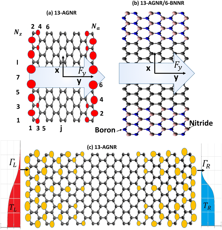 | ||
| Fig. 1 (a) and (b) Schematic diagrams illustrating the armchair graphene nanoribbon (13-AGNR) and 13-AGNR/6-BNNR heterojunction under longitudinal electric fields, respectively. Schematic diagram (c) depicts the line-contacting of zigzag-edge atoms in a 13-AGNR structure to electrodes. Symbols ΓL(ΓR) represent the electron tunneling rate between the left (right) electrode and the leftmost (rightmost) atoms at the zigzag edges, and TL(TR) denotes the equilibrium temperature of the left (right) electrode. The probability densities of the zigzag edge states with short and long characteristic lengths in 13-AGNR segments without electric fields are plotted in (a) and (c), respectively. The radius of the circle represents the magnitude of the probability density. | ||
2 Calculation methodology
To investigate the transport properties of 13-AGNR and 13-AGNR/6-BNNR heterojunctions connected to the electrodes, we employ a combination of the tight-binding model and the Green's function technique. The system Hamiltonian depicted in Fig. 1(c) is written as H = H0 + HGNR, where
 | (1) |
The first two terms of eqn (1) describe the free electrons in the left and right metallic electrodes. a†k(b†k) creates an electron of with momentum k and energy εk in the left (right) electrode. 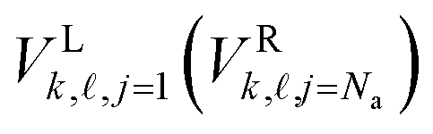 describes the coupling between the left (right) lead with its adjacent atom in the
 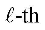 row.
row.
 | (2) |
 represents the on-site energy of the orbital in the
  row and j-th column. The operators
  and
and  create and annihilate an electron at the atom site denoted by
  . The parameter
  characterizes the electron hopping energy from site
  to site
  . For the tight-binding parameters of n-AGNR/w-BNNR, we assign EB = 2.329 eV, EN = −2.499 eV, and EC = 0 eV to boron, nitride, and carbon atoms, respectively. We neglect variations in electron hopping strengths between different atoms for simplicity.29,30 We set
  for the nearest-neighbor hopping strength. Additionally, the effect of electric field Fy is included by the electric potential U = eFyy on
  , where Fy = Vy/La, with Vy as the applied bias and La as the length of the AGNR segment.
We calculate the bias-dependent transmission coefficient  using the formula:
  ,26 where ΓL(ε) and ΓR(ε) denote the tunneling rate (in energy units) at the left and right leads, respectively, and Gr(ε) and Ga(ε) are the retarded and advanced Green's functions of the GNRs, respectively. In terms of tight-binding orbitals, Γα(ε) and Green's functions are matrices. The expression for ΓL(R)(ε) is derived from the imaginary part of the self-energies, denoted as
  , and is given by
  , where
  and
and  denote the coupling strengths between the left and right metallic electrodes with their adjacent atoms (refer to Fig. 1). In the context of metals such as gold, where the density of states remains approximately constant near the Fermi energy, the wide-band limit serves as a suitable approximation. In this limit, the energy-dependent tunneling rates, ΓL(R)(ε), are replaced by constant matrices denoted as ΓL(R).26 However, it's important to note that in some cases, only the diagonal entries of ΓL(R) are non-zero. Additionally, if one adopts the alternative definition of
  , the factor “4′′ in the transmission coefficient is reset to one.31–33 Notably, ΓL(R) calculated within the wide-band limit can effectively replicate the transmission coefficient curves of graphene nanoribbon superlattices obtained using the surface Green's function method, as demonstrated in ref. 32 and 33.
3 Results and discussion
Before examining the effects of electric fields on the electronic and transport properties of end zigzag edge states of 13-AGNR and 13-AGNR/6-BNNR structures, we first present the electronic structures of these two configurations in Fig. 2(a) and (b), respectively. Both structures maintain semiconductor properties with direct band gaps. Specifically, the 13-AGNR and 13-AGNR/6-BNNR exhibit band gaps of 0.714 eV and 0.722 eV, respectively, consistent with values calculated by the DFT method.30 It's noteworthy that the electronic structures of 13-AGNR/w-BNNR remain unchanged when w ≥ 6. This suggests that a 6-BNNR width is sufficient to model 13-AGNR embedded within an h-BN sheet. Although the impact of BNNR on the band gaps of 13-AGNRs is not significant, we will demonstrate later that BNNR structures have a notable effect on the end zigzag edge states of 13-AGNRs.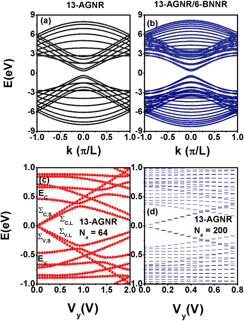 | ||
| Fig. 2 Electronic structures of 13-AGNR and 13-AGNR/6-BNNR structures. (a) 13-AGNR structure and (b) 13-AGNR/6-BNNR structure. Energy levels of 13-AGNRs as functions of applied voltage Vy for two different Na values. (c) Na = 64 (La = 6.67 nm) and (d) Na = 200 (La = 21.16 nm). Note that the energy levels are plotted with respect to the Fermi energy EF, which is set as zero throughout this article. | ||
3.1 13-AGNR segments under an electric field
To elucidate the end zigzag edge states of 13-AGNRs, we analyze the energy spectra of 13-AGNR segments under an electric field. Fig. 2(c) and (d) illustrate the energy levels of 13-AGNR segments with Na = 64 (La = 6.67 nm) and Na = 200 (La = 21.16 nm) as functions of Vy. In the absence of an electric field, four energy levels exist between EC and EV, representing the subband states as depicted in Fig. 2(c). These levels are denoted as ΣC,S, ΣC,L, ΣV,S, and ΣV,L. Here, C and V distinguish the energy levels above or below the Fermi energy, while S and L represent short and long decay characteristic lengths, respectively. These levels arise from the formation of bonding and antibonding states between the left and right TSs (ΨL,S(L) and ΨR,S(L)), as noted in ref. 19. For Na = 64, ΣC(V),L = ±7.13 meV and ΣC(V),S = 0. For Na = 200, ΣC(V),L = ±7 μeV and ΣC(V),S = 0. When considering Na = 200, EC and EV are 0.3668 eV and −0.3668 eV, respectively, which closely correspond to the minimum conduction subband and the maximum valence subband of infinitely long 13-AGNRs shown in Fig. 2(a). Notably, in Fig. 2(c) and (d), we observe a blue Stark shift of TSs and a red Stark shift of the subband states. Consequently, the energy levels of end zigzag edge states cross the subband states. With increasing Na, the applied bias inducing such a crossing is shifted toward lower bias, as observed in Fig. 2(d). Note that the Stark shift of energy levels for graphene nanoribbon (GNR) segments (or graphene quantum dots) responds sensitively to the applied electric fields, with directionality playing a crucial role.34,35 Particularly, when transverse electric fields (Fx) are introduced to armchair graphene nanoribbons (AGNRs), we observe an intriguing semiconductor-to-semimetal transition in the electronic structures.13,15To further comprehend the charge transport through these topological states (ΨL(R),S and ΨL(R),L), we plot the transmission coefficient  of a 13-AGNR segment with Na = 64 for various Vy values in Fig. 3(a)–(c). As depicted in Fig. 3(a), the peak labeled by Σ0 arises from ΣC,L and ΣV,L, rather than ΣC,S and ΣV,S, as their wave functions (ΨL,S and ΨR,S) are highly localized on the end zigzag edges (see Fig. 1(a)). With the application of bias voltage Vy in Fig. 3(b), the probability for charge tunneling through these topological states diminishes significantly due to the off-resonance energy levels of ΨL,L and ΨR,L. Upon reaching Vy = 0.918 V, two peaks labeled εC(V),B and εC(V),A emerge due to the interference between the end zigzag edge states ΣC(V),L and the subband states EC(V), as seen in Fig. 3(c). The peak at εC(V),B can be interpreted as charge tunneling through the long decay length edge state under the subband states (EC(V)) assisted procedure. Fig. 3(d) illustrates the contact effect on this interference phenomenon. As Γt decreases, the resolution between the peaks (εC,B and εC,A) becomes more distinct. For Γt = 90 meV, the interference pattern resembles Fano interference. The probability distributions of the peaks labeled εC,B and εC,A are shown in Fig. 3(e) and (f), respectively. It is evident that εC(V),B and εC(V),A correspond to constructive and destructive interferences between the wave function of the conduction (valence) subband state and the wave function of the right (left) edge state with a long characteristic length (ΨR(L),L). Although many theoretical efforts predict the existence of topological states of GNRs,10–12 revealing the quantum interference between the TSs and the subband states based on the tunneling spectra of GNR-based electronic devices remains a challenge.8,9
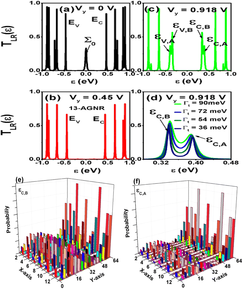 | ||
Fig. 3 Transmission coefficients  of 13-AGNRs with Na = 64 for various Vy values at Γt = 0.09 eV. Panels (a), (b), and (c) correspond to Vy = 0, Vy = 0.45 V, and Vy = 0.918 V, respectively. Panel (d) shows the of 13-AGNRs with Na = 64 for various Vy values at Γt = 0.09 eV. Panels (a), (b), and (c) correspond to Vy = 0, Vy = 0.45 V, and Vy = 0.918 V, respectively. Panel (d) shows the  for various Γt values at Vy = 0.918 V. Panels (e) and (f) depict probability densities of εC,B = 0.337 eV and εC,A = 0.393 eV in a 13-AGNR segment with Na = 64 and Vy = 0.918 V. for various Γt values at Vy = 0.918 V. Panels (e) and (f) depict probability densities of εC,B = 0.337 eV and εC,A = 0.393 eV in a 13-AGNR segment with Na = 64 and Vy = 0.918 V. | ||
3.2 13-AGNR/6-BNNR segments under an electric field
Considering the influence of h-BN on the electronic and transport properties of 13-AGNRs, we present the energy levels of 13-AGNR/6-BNNR structures as functions of applied Vy for various Na values in Fig. 4(a)–(c). In the gap region of the 13-AGNR/6-BNNR structure (refer to Fig. 2(b)), there are still four energy levels present (ΣC,S, ΣC,L, ΣV,S, and ΣV,L). Unlike the multiple end zigzag edge states of 13-AGNRs, the multiple zigzag edge states of finite 13-AGNR/6-BNNR heterojunctions are insensitive to variations in Na, remaining nearly fixed at specific energy levels. For instance, at Na = 44, we have ΣC,S = 76.4 meV (ΣV,S = −81.7 meV) and ΣC,L = 0.253 eV (ΣV,L = −0.268 eV). Similarly, at Na = 64, we observe ΣC,S = 76.4 meV (ΣV,S = −81.7 meV) and ΣC,L = 0.249 eV (ΣV,L = −0.263 eV). This indicates that ΣC,S, ΣC,L, ΣV,S, and ΣV,L are not determined by the wave function overlaps between the left and right TSs. In finite 13-AGNR/6-BNNR heterojunctions, BNNRs have the left boron atom zigzag edge terminal and the right nitride atom zigzag edge terminal (see Fig. 1(b)). The energy levels of ΣC,S, ΣC,L, ΣV,S, and ΣV,L are significantly influenced by the energy levels of boron and nitride atoms.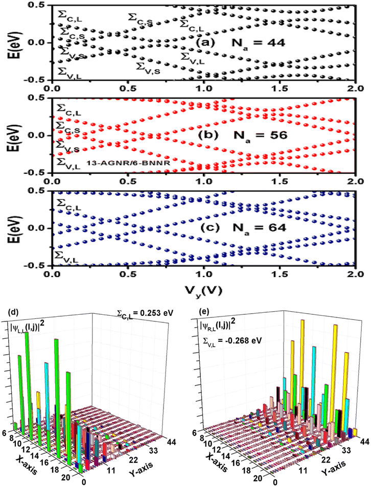 | ||
| Fig. 4 Energy levels of 13-AGNR/6-BNNR heterojunction as functions of Vy for various Na. Panels (a), (b), and (c) correspond to Na = 44 (La = 4.54 nm), Na = 56 (La = 5.82 nm), and Na = 64 (La = 6.67 nm), respectively. Probability densities of 13-AGNR/6-BNNR heterojunction with Na = 44 (La = 4.54 nm) at Vy = 0. Panels (d) and (e) depict the probability densities of ΣC,L and ΣV,L, respectively. | ||
Fig. 4(a)–(c) indicate that the multiple zigzag edge states of 13-AGNR/6-BNNR exhibit a linear function of the electric field. In the high bias region (Vy > 1 V), the interaction spectra resulting from the multiple end zigzag edge states and the subband states can be reproduced, akin to the interference scenario observed in 13-AGNRs (Fig. 2(c) and (d)). Before calculating the transmission coefficient of 13-AGNR/6-BNNR heterojunction, we plot the probability densities of ΣC,L and ΣV,L at Vy = 0 and Na = 44 in Fig. 4(d) and (e), respectively. From the probability distributions of ΣC,L and ΣV,L, it is evident that charges are confined within the 13-AGNR segment, demonstrating that BNNRs act as potential barriers. Additionally, ΣC,L(ΣV,L) is determined by the unoccupied carbon–nitride antibonding state (occupied carbon–boron bonding state).36,37
The maximum probability of ΣC,L(ΣV,L) occurs at sites labeled by  and
and  at j = 1 (
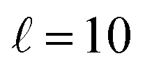 and
and  at j = 44). The probability distribution of ΣC,L(ΣV,L) along the y direction exhibits a long decay length, spanning several benzene sizes, yet its probability density near the right (left) electrode sites is minimal. This indicates that the wave function of ΣC,L(ΣV,L) is weakly coupled to the right (left) electrode. The asymmetrical coupling to the left and right electrodes for the wave function of ΣC,L(ΣV,L) hinders charge transport through this energy level.
We now present the calculated transmission coefficient of the 13-AGNR/6-BNNR heterojunction with Na = 44 for various applied bias Vy values at Γt = 90 meV in Fig. 5. In Fig. 5(a) and (b), the charge transport through ΣC,L and ΣV,L is hindered due to the very weak coupling strength between the electrodes and the zigzag edge states. However, a significant peak of Σ0 occurs for ε near the Fermi energy at Vy = 0.702 V in Fig. 5(c). For Vy = 1.02 V and Vy = 1.458 V, the peaks for charge transport through ΣC,L and ΣV,L are shifted away from the Fermi energy, as shown in Fig. 5(d) and (e). A notable enhancement of charge transport through ΣC,L and ΣV,L is observed for Vy = 1.62 V, which is attributed to the assistance from subband states.
 | ||
Fig. 5 Transmission coefficient  of the 13-AGNR/6-BNNR heterojunction with Na = 44 for various Vy values at Γt = 90 meV. Panels (a) through (f) correspond to Vy values of 0, 0.378 V, 0.702 V, 1.02 V, 1.458 V, and 1.62 V, respectively. Panel (g) displays the probability distribution of Σ0 = 0 at Vy = 0.702 V. Panel (h) shows the transmission coefficient of the 13-AGNR/6-BNNR heterojunction with Na = 44 for various Vy values at Γt = 90 meV. Panels (a) through (f) correspond to Vy values of 0, 0.378 V, 0.702 V, 1.02 V, 1.458 V, and 1.62 V, respectively. Panel (g) displays the probability distribution of Σ0 = 0 at Vy = 0.702 V. Panel (h) shows the transmission coefficient  as functions of ε for various Γt values at Vy = 0.702 V. as functions of ε for various Γt values at Vy = 0.702 V. | ||
The transmission coefficient of Σ0 shown in Fig. 3(c) is attributed to the alignment between ΣC,L and ΣV,L. We plot the probability distribution of Σ0 = 0 in Fig. 5(g). The symmetrical probability distribution explains the alignment of ΣC,L and ΣV,L. As these two levels approach alignment, their wave functions  and
and  generate constructive and destructive superpositions, forming the two splitting peaks. To resolve these two peaks, we present the transmission coefficient
  for various Γt values in Fig. 5(h). The results in Fig. 5(h) indicate that the transmission coefficient is affected not only by the applied voltage but also by the contact property between the electrodes and the 13-AGNR/6-BNNR heterojunctions. For weak Γt = 36 meV, we observe two separated peaks.
3.3 Tunneling current through the zigzag edge states of 13-AGNR/6-BNNR heterojunctions
In this subsection, we investigate the tunneling current through the end zigzag edge states with long decay length, utilizing the effective 2-site Hubbard model.38 The transmission coefficient curves depicted in Fig. 3(d) and 5(h) can be faithfully replicated by the effective 2-site Hubbard model, as the zigzag edge states are well-separated from the subband states under low applied bias, and their wave functions are localized.27 The tunneling current is determined by the expression:
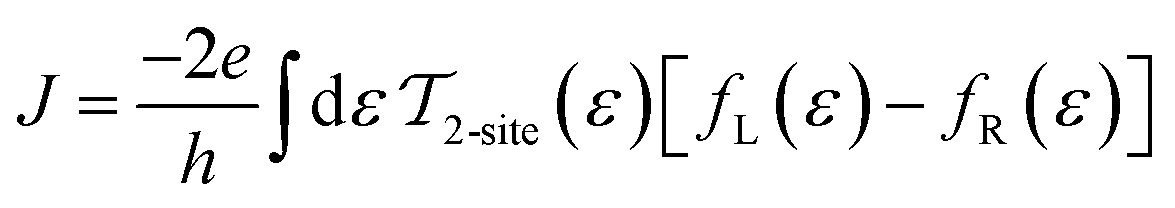 | (3) |
 , includes one-particle, two-particle, and three-particle correlation functions in the Coulomb blockade region, computed self-consistently.39 Furthermore, the bias-independent intra-site (U0) and inter-site (U1) Coulomb interactions are computed using
  with the dielectric constant ε0 = 4, and Ucc = 4 eV at i = j. Ucc arises from the two-electron occupation in each pz orbital. In Fig. 6, the non-interaction curve corresponds to the case depicted in Fig. 4(c). The inset of Fig. 6 illustrates charge transport in the Coulomb blockade region, where εC,L = ΣC,L − ηeVy + iΓe,L and εV,L = ΣV,L + ηeVy + iΓe,R. Here, ηeVy = 0.336eVy represents the orbital offset terms induced by the applied voltage (Vy), and Γe,L = Γe,R = Γe,t represents the effective tunneling rate of end zigzag states in the 2-site model, determined by Γt and the wave functions of the edge states ΨC(V),L.
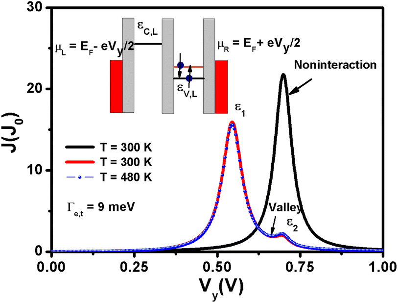 | ||
| Fig. 6 Tunneling current through the end zigzag edge state with a long decay length of the 13-AGNR/6-BNNR heterojunction with Na = 64. Energy levels are defined as εC,L = ΣC,L − 0.366eVy + iΓe,L and εV,L = ΣV,L + 0.366eVy + iΓe,R. Other physical parameters include ΣC,L = 0.249 eV, ΣV,L = −0.263 eV, intra-site Coulomb interaction U0 = 155 meV, inter-site Coulomb interaction U1 = 42 meV, and inter-site electron hopping strength tLR = 7.13 meV. We have Γe,L = Γe,R = Γe,t = 9 meV, EF = 0, and J0 = 0.773 nA. | ||
The first peak of the red curve, calculated at temperature T = 300 K and labeled ε1, corresponds to the charge transfer from εV,L + U0 to εC,L when these two energy levels align. The second peak, ε2, corresponds to electron transfer between εV,L and εC,L. However, the tunneling current for such a procedure is significantly suppressed due to electron Coulomb interactions. The blue curve with markers is calculated at T = 480 K. Distinguishing between the red and blue curves in the entire applied voltage region is challenging, illustrating the nonthermal broadening effect of the tunneling current. Additionally, the peak-to-valley ratio reaches 8.7. The results presented in Fig. 6 demonstrate that the edge states with long decay length act as effective single charge filters at room temperature, suggesting their potential application in single-electron transistors at room temperature.40 Traditional single electron transistors formed by a single quantum dot exhibit temperature-dependent tunneling current spectra,41–43 where the peak-to-valley ratio of tunneling current tends to decrease with increasing temperature. Our study demonstrates that the tunneling current through the zigzag edge states of 13-AGNR/6-BNNR heterojunctions maintains temperature stability, a significant advantage for practical applications.
4 Conclusion
In this study, we investigated the charge transport properties through the multiple end zigzag edge states of both 13-AGNR and 13-AGNR/6-BNNR heterojunctions under longitudinal electric fields, employing the tight-binding model and Green's function technique. For 13-AGNRs, we elucidated the distinct blue Stark shift behaviors exhibited by the zigzag edge states with short and long decay lengths in response to electric fields. We found that the latter can significantly interact with the subband states, thereby unveiling the mechanism of charge transport through the long decay length zigzag edge states assisted by the subband states, as evidenced by the spectra of the transmission coefficient.Concerning 13-AGNR/6-BNNR heterojunctions, we observed that the energy levels of the end zigzag edge states of 13-AGNRs are notably influenced by the presence of BNNRs rather than their lengths. Even in long 13-AGNR/6-BNNR segments, ΣC,L exhibits a significant orbital offset from ΣV,L. We further revealed a remarkable resonant tunneling process for charge transfer between ΣC,L and ΣV,L through the bias-dependent transmission coefficient analysis.
Moreover, employing a 2-site Hubbard model, we analyzed the tunneling current through the end zigzag edge states of 13-AGNR/6-BNNR heterojunctions within the Coulomb blockade region. Our results demonstrate that these edge states function effectively as single charge filters at room temperature, exhibiting a high peak-to-valley ratio of tunneling current with a nonthermal broadening effect, as illustrated in Fig. 6. This unique characteristic suggests promising applications of 13-AGNR/6-BNNR heterojunctions in single electron transistors operating at room temperature.
Data availability
The data presented in this study are available upon reasonable request.Conflicts of interest
There are no conflicts to declare.Acknowledgements
This work was supported by the National Science and Technology Council, Taiwan under Contract No. MOST 107-2112-M-008-023MY2.References
- K. S. Novoselov, A. K. Geim, S. V. Morozov, D. Jiang, Y. Zhang, S. V. Dubonos, I. V. Grigorieva and A. A. Firsov, Electric field effect in atomically thin carbon films, Science, 2004, 306, 666 CrossRef CAS PubMed.
- J. Haskins, A. Kinaci, C. Sevik, H. Sevincli, G. Cuniberti and T. Cagin, Control of Thermal and Electronic Transport in Defect-Engineered Graphene Nanoribbons, ACS Nano, 2011, 5, 3779–3787 CrossRef CAS PubMed.
- P. H. Chang, M. S. Bahramy, N. Nagaosa and B. K. Nikolic, Giant Thermoelectric Effect in Graphene-Based Topological Insulators with Heavy Adatoms and Nanopores, Nano Lett., 2014, 14, 3779–3784 CrossRef CAS PubMed.
- H. M. Wang, H. S. Wang, C. X. Ma, L. X. Chen, C. X. Jiang, C. Chen, X. M. Xie, A. P. Li and X. R. Wang, Graphene nanoribbons for quantum electronics, Nat. Rev. Phys., 2021, 3, 791 CrossRef CAS.
- J. Cai, P. Ruffieux, R. Jaafar, M. Bieri, T. Braun, S. Blankenburg, M. Muoth, A. P. Seitsonen, M. Saleh, X. Feng, K. Mullen and R. Fasel, Atomically precise bottom-up fabrication of graphene nanoribbons, Nature, 2010, 466, 470 CrossRef CAS PubMed.
- J. Z. Liu, B. W. Li, Y. Z. Tan, A. Giannakopoulos, C. Sanchez-Sanchez, D. Beljonne, P. Ruffieux, R. Fasel, X. L. Feng and K. Mullen, Toward Cove-Edged Low Band Gap Graphene Nanoribbons, J. Am. Chem. Soc., 2015, 137, 6097 CrossRef CAS.
- Y. C. Chen, T. Cao, C. Chen, Z. Pedramraz, D. Haberer, D. G. de Oteyza, R. Fischer, S. G. Louie and M. F. Crommie, Molecular bandgap engineering of bottom-up synthesized graphene nanoribbon heterojunctions, Nat. Nanotechnol., 2015, 10, 156 CrossRef CAS PubMed.
- J. P. Llinas, A. Fairbrother, G. Borin Barin, W. Shi, K. Lee, S. Wu, B. Y. Choi, R. Braganza, J. Lear and N. Kau, et al., Short-channel field-effect transistors with 9-atom and 13-atom wide graphene nanoribbons, Nat. Commun., 2017, 8, 633 CrossRef PubMed.
- P. H. Jacobse, A. Kimouche, T. Gebraad, M. M. Ervasti, J. M. Thijssen, P. Liljeroth and I. Swart, Electronic components embedded in a single graphene nanoribbon, Nat. Commun., 2017, 8, 119 CrossRef CAS PubMed.
- D. J. Rizzo, G. Veber, J. W. Jiang, R. McCurdy, T. Bronner, T. Cao, T. Chen, S. G. Louie, F. R. Fischer and M. F. Crommie, Inducing metallicity in graphene nanoribbons via zero-mode superlattices, Science, 2020, 369, 1597 CrossRef CAS PubMed.
- Q. Sun, Y. Yan, X. L. Yao, K. Mullen, A. Narita, R. Fasel and P. Ruffieux, Evolution of the Topological Energy Band in Graphene Nanoribbons, J. Phys. Chem. Lett., 2021, 12, 8679 CrossRef CAS PubMed.
- D. J. Rizzo, J. W. Jiang, D. Joshi, G. Veber, C. Bronner, R. A. Durr, P. H. Jacobse, T. Cao, A. Kalayjian, H. Rodriguez, P. Butler, T. Chen, S. G. Louie, F. R. Fischer and M. F. Crommie, Rationally Designed Topological Quantum Dots in Bottom-Up Graphene Nanoribbons, ACS Nano, 2021, 15, 20633 CrossRef CAS.
- F. Z. Zhao, T. Cao and S. G. Louie, Topological Phases in Graphene Nanoribbons Tuned by Electric Fields, Phys. Rev. Lett., 2021, 127, 166401 CrossRef CAS.
- X. Wang, Y. Q. Cui, L. Zhang and M. L. Yang, Enhanced second-order Stark effect in twisted bilayer graphene quantum dots, Nano Res., 2021, 14, 3935 CrossRef CAS.
- M. Pizzochero, N. V. Tepliakov, A. A. Mostofi and E. Kaxiras, Electrically Induced Dirac Fermions in Graphene Nanoribbons, Nano Lett., 2021, 21, 9332 CrossRef CAS.
- V. T. Nikita, M. Ruize, L. Johannes, K. Efthimios, A. M. Arash and P. Michele, Dirac Half-Semimetallicity and Antiferromagnetism in Graphene Nanoribbon/Hexagonal Boron Nitride Heterojunctions, Nano Lett., 2023, 23, 6698 CrossRef.
- N. V. Tepliakov, J. Lischner, E. Kaxiras, A. A. Mostofi and M. Pizzochero, Unveiling and Manipulating Hidden Symmetries in Graphene Nanoribbons, Phys. Rev. Lett., 2023, 130, 026401 CrossRef CAS.
- M. Golor, C. Koop, T. C. Lang, S. Wessel and M. J. Schmidt, Magnetic correlations in short and narrow graphene armchair nanoribbons, Phys. Rev. Lett., 2013, 111, 085504 CrossRef PubMed.
- M. P. Lopez-Sancho and M. Carmen Munoz, Topologically protected edge and confined states in finite armchair graphene nanoribbons and their junctions, Phys. Rev. B: Condens. Matter Mater. Phys., 2021, 104, 245402 CrossRef CAS.
- A. D. Zdetsis, Peculiar electronic properties of wider armchair graphene nanoribbons: Multiple topological end-states and ”phase transitions”, Carbon, 2023, 210, 118042 CrossRef CAS.
- L. X. Chen, L. He, H. S. Wang, H. M. Wang, S. J. Tang, C. X. Cong, H. Xie, L. Li, H. Xia and T. X. Li, Oriented graphene nanoribbons embedded in hexagonal boron nitride trenches, Nat. Commun., 2017, 8, 14703 CrossRef PubMed.
- H. S. Wang, L. X. Chen, K. Elibol, L. He, H. M. Wang, C. Chen, C. X. Jiang, C. Li, T. R. Wu and C. X. Cong, Towards chirality control of graphene nanoribbons embedded in hexagonal boron nitride, Nat. Mater., 2021, 20, 202 CrossRef CAS PubMed.
- D. C. Geng, I. Abdelwahab, X. F. Xiao, A. Cernescu, W. Fu, V. Giannini, S. A. Maier, L. Li, W. P. Hu and K. P. Loh, One-Pot Confined Epitaxial Growth of 2D Heterostructure Arrays, ACS Mater. Lett., 2021, 3, 217 CrossRef CAS.
- Y. W. Son, M. L. Cohen and S. G. Louie, Energy Gaps in Graphene Nanoribbons, Phys. Rev. Lett., 2006, 97, 216803 CrossRef PubMed.
- Y. Matsuda, W. Q. Deng and W. A. Goddard III, Contact Resistance for ”End-Contacted” Metal-Graphene and Metal-Nanotube Interfaces from Quantum Mechanics, J. Phys. Chem. C, 2010, 114, 17845 CrossRef CAS.
- D. M. T. Kuo and Y. C. Chang, Contact Effects on Thermoelectric Properties of Textured Graphene Nanoribbons, Nanomaterials, 2022, 12, 3357 CrossRef CAS.
- D. M. T. Kuo, Effects of Coulomb Blockade on the Charge Transport through the Topological States of Finite Armchair Graphene Nanoribbons and Heterostructures, Nanomaterials, 2023, 13, 1757 CrossRef CAS.
- D. M. T. Kuo, Thermal rectification through the topological states of asymmetrical length armchair graphene nanoribbons heterostructures with vacancies, Nanotechnology, 2023, 34, 505401 CrossRef.
- G. S. Seal and J. Guo, Bandgap opening in boron nitride confined armchair graphene nanoribbon, Appl. Phys. Lett., 2011, 98, 143107 CrossRef.
- Y. Ding, Y. Wang and J. Ni, Electronic properties of graphene nanoribbons embedded in boron nitride sheets, Appl. Phys. Lett., 2009, 95, 123105 CrossRef.
- Q. F. Sun and X. C. Xie, CT-Invariant Quantum Spin Hall Effect in Ferromagnetic Graphene, Phys. Rev. Lett., 2010, 104, 066805 CrossRef.
- X. U. Ning, B. L. Wang, H. Q. Sun and J. W. Ding, Resonance Transmission in Graphene-Nanoribbons-Based Quantum Dot and Superlattice, Chin. Phys. Lett., 2010, 10, 107303 CrossRef.
- X. X. Yu and Y. E. Xie, Spin-Polarized transport in graphene nanoribbon superlattices, Chin. Phys. B, 2012, 10, 107202 CrossRef.
- R. B. Chen, C. P. Chang and M. F. Lin, Electric-field-tunable electronic properties of graphene quantum dots, Physica E, 2010, 42, 2812 CrossRef CAS.
- T. G. Pedersen, Stark effect and polarizability of graphene quantum dots, Phys. Rev. B, 2017, 96, 115432 CrossRef.
- J. M. Pruneda, Origin of half-semimetallicity induced at interfaces of C-BN heterostructures, Phys. Rev. B: Condens. Matter Mater. Phys., 2010, 81, 161409(R) CrossRef.
- J. Jung, Z. H. Qiao, Q. Niu and A. H. MacDonald, Transport Properties of Graphene Nanoroads in Boron Nitride Sheets, Nano Lett., 2012, 12, 2936 CrossRef CAS PubMed.
- M. J. J. Mangnus, F. R. Fischer, M. F. Crommie, I. Swart and P. H. Jacobse, Charge transport in topological graphene nanoribbons and nanoribbon heterostructures, Phys. Rev. B, 2022, 105, 115424 CrossRef CAS.
- D. M. T. Kuo, S. Y. Shiau and Y. C. Chang, Theory of spin blockade, charge ratchet effect, and thermoelectrical behavior in serially coupled quantum dot system, Phys. Rev. B: Condens. Matter Mater. Phys., 2011, 84, 245303 CrossRef.
- Y. M. Lee, E. B. Song and T. Hiramoto, Observation of Single Electron Transport via Multiple Quantum States of a Silicon Quantum Dot at Room Temperature, Nano Lett., 2014, 14, 71 CrossRef PubMed.
- E. Leobandung, L. J. Guo, Y. Wang and S. Y. Chou, Observation of quantum effects and Coulomb blockade in silicon quantum-dot transistors at temperatures over 100 K, Appl. Phys. Lett., 1995, 67, 938 CrossRef CAS.
- L. Zhuang, L. J. Guo and S. Y. Choub, Silicon single-electron quantum-dot transistor switch operating at room temperature, Appl. Phys. Lett., 1998, 72, 1205 CrossRef CAS.
- H. W. C Postma, T. Teepen, Z. Yao, M. Grifoni and C. Dekker, Carbon Nanotube Single-Electron Transistors at Room Temperature, Science, 2001, 293, 76 CrossRef PubMed.
| This journal is © The Royal Society of Chemistry 2024 |