DOI:
10.1039/D4RA02429J
(Paper)
RSC Adv., 2024,
14, 23873-23885
Structural and optical properties of phosphorous doped nanocrystalline silicon deposited using a VHF PECVD process for silicon heterojunction solar cells and optimization of a simple p–n junction cell using SCAP-1D tool†
Received
30th March 2024
, Accepted 22nd July 2024
First published on 30th July 2024
Abstract
Initially hydrogenated silicon (Si:H) thin films have been deposited using a plasma-enhanced chemical vapor deposition technique (PECVD) using silane (SiH4) as a precursor gas diluted in an inert gas argon (Ar) environment. Subsequently phosphine gas (PH3) was used as the n-type dopant and the deposition was carried out at a fixed substrate temperature of 200 °C. The PH3 flow rate was varied in the range of 0–1 sccm. The effect of PH3 flow rates on optical, electrical, and structural properties of hydrogenated amorphous and micro/nanocrystalline silicon films has been investigated and detailed analysis is presented. These films may find application in heterojunction solar cells as an emitter layer. Further, a crystalline silicon (c-Si) based simple p–n junction solar cell is simulated using an SCAP-1D tool to observe the effect of layer thickness and doping density on solar cell parameters.
1 Introduction
In solar cells, the emitter layer has an important role to obtain high power conversion efficiency (PCE) in heterojunction/homojunction devices. The n/p type amorphous silicon emitter layer on the surface of an n/p type crystalline wafer has attracted significant interest due to cost effectiveness and high PCE.1,2 But these devices consisting of amorphous silicon as an emitter layer show more parasitic absorption loss and lower doping efficiency.3,4 However hydrogenated amorphous silicon (a-Si:H) has also been used in heterojunction solar cells but these devices are less stable due to the presence of hydrogen related defects.5 As an alternative to the amorphous layer, a nanocrystalline silicon (nc-Si) emitter layer has shown excellent results including enhanced stability under light exposure and high doping efficiency.6 Shah et al.7 synthesized nc-Si:H and embedded it as an absorber layer in the solar cells achieving an efficiency of 10.1%. Using nc-Si:H in tandem/micromorph solar cells, Yamamoto et al.8 reported an initial efficiency of ∼14.7%. The hydrogenated crystalline silicon (c-Si:H) devices shows good stability, higher carrier mobility and better performance against light induced degradation as compared to a-Si:H. The hydrogenated micro/nanocrystalline silicon (μc/nc-Si:H) films consisting of impurity atoms possess desirable properties and improved conductivity, reduced activation energy (Ea) and good photo thermal stability.9 However a-Si:H has been widely used in heterojunction (HIT) solar cells both as passivating and emitter layer and the use of n-doped μc/nc-Si:H has also shown excellent result as an emitter layer in HIT solar cells.10
The essential requirement is to develop high quality n type nanocrystalline silicon layer (nc-Si:H) on p type wafer via efficient doping. The amount of doping in thin films controls the performance of the devices. The higher conductivity in n type silicon films can be obtained under controlled PH3 doping. But heavy doping also reduces crystalline nature in silicon network.11 Thus, at low temperature, high hydrogen dilution in the plasma is mostly used to achieve crystallinity. A combination of both hydrogen and noble gas can also be used to obtain crystallinity.
Scientists have used different techniques to obtain good quality n type nc-Si:H films under controlled doping such as plasma enhanced chemical vapor deposition (PECVD), microwave PECVD,12 electron beam evaporation,13 electron cyclotron resonance PECVD,14 Si ion implantation,15 hot wire CVD,16 cathodic vacuum arc,17 RF magnetron sputtering18 etc. Furthermore, in case of selection of wafer, n type possess lower defect density, low recombination rate of charge carriers at the interface and even high resistance against degradation10 than p type wafer. But the major concern is high production cost of n type ingots and hence less availability in the market. Thus, it is better to explore heterojunction solar cells with p type wafers.
The n-type hydrogenated micro/nanocrystalline silicon films can be achieved by precisely controlling the process parameters during deposition by PECVD. However, surplus doping atoms generates defects that hinder crystallization in the network and results in lower doping efficiency. Accordingly, optimization of parameters and integration of optimum dopants remains primary task to maintain crystallinity. There are only few reports available giving comprehensive investigation and influence of various deposition parameters on electrical, optical and structural properties with the correlation among other properties of PH3 doped silicon films developed by PECVD.19
In the present work PH3 doped n type nc-Si:H has been developed at low substrate temperature of 200 °C. The deposition of n-type nc-Si:H films with high conductivity of 0.18 S cm−1 has been carried out at very high frequency (VHF) PECVD process with appreciably high deposition rate. The PECVD process supplies low defect density and high doping efficiency in large area thin films at low temperature.20 We systematically investigate the influence of PH3 doping on the microstructural and optoelectronic properties of n-type nc-Si:H thin films grown by PECVD at low substrate temperature of 200 °C. The electrical as well as structural properties were found to correlate very well. The use of nc-Si:H films with high conductivity would replace a-Si:H films to overcome the Staebler–Wronski effect, improving diffusion length, more carrier life time and charge carrier mobility for high PCE solar cells.21,22 Structural morphology at different doping of PH3 has been studied to obtain suitable optoelectronic properties of nanocrystalline silicon network for solar cell.
Further numerical modelling of crystalline silicon (c-Si) based simple p–n junction solar cell is carried out using solar cell capacitance simulator (SCAP-1D) tool to observe the effect of layer thickness and doping density on solar cell parameters.
2 Experimental and simulation details
The PH3 doped n-type nc-Si:H films were deposited in very high frequency assisted plasma enhanced chemical vapor deposition (PECVD) system using silane (SiH4) as precursor and PH3 as a dopant gas, having ladder shape geometry. The PH3 flow rates was varied in the range of 0–1 sccm while all other parameters were kept constant. The substrate temperature was fixed at 200 °C. These films were deposited on Corning 7059 glass, ITO coated class and silicon substrates. The PECVD system consists of a vacuum chamber, valves and pumps, flow controller, a ladder-shaped electrode and a very high frequency (VHF) power source (Fig. S1†). The structural properties were analyzed by Raman spectroscopy (LABRAM HR 800 Horiba JY) and X-ray diffraction (XRD). The XRD measurement was performed using RigakuUltima IV diffractometer with Cu Ka radiation (k = 1.54 Å). The doped micro/nano crystalline silicon films presented a crystallographic orientation preferentially in the (1 1 1) and (2 2 0) plane. The optical properties were studied using UV visible spectroscopy (PerkinElmer Ultraviolet–visible Spectrometer) in the range 350–1240 nm to deduce the optical band gap of the deposited films. Correlations between structural, optical and electrical properties have also been studied. Room temperature and temperature dependent conductivity measurements were performed on samples and contacts were made in coplanar geometry using aluminum (Al) through shadow mask prepared by thermal evaporation technique. The conductivity measurement was done in vacuum at 10−4 torr using a Keithley 617 programmable electrometer, and coplanar geometry with an effective gap of 0.078 cm between the electrodes. The field emission scanning electron microscopy (FESEM) images were obtained using NOVA NANO SEM 450, FEI electron microscope to characterize the surface morphology of films.
The electrical conductivity of samples measured at room temperature varies in the order of 10−5 S cm−1 (minimum) to 0.18 S cm−1 (maximum) for the n-doped films. Meanwhile, the activation energy decreased to 0.18 eV from maximum value of 0.7 eV for the PH3 doped film and hence higher conductivity can be achieved in Si films with doping. These n doped films may increase charge generation in solar cells and also PCE in amorphous and micro/nano crystalline silicon solar cells. These deposited n layer film can be useful as an emitter layer in crystalline silicon bulk heterojunction solar cells to achieve high PCE. For simulation purpose SCAP-1D simulation tool has been used under AM1.5 G (100 mW cm−2) solar spectrum with 300 Kelvin temperature. This SCAP software which is one dimensional can be used to solve basic semiconductor equations, boundary conditions, Poisson's equation etc., to study and simulate properties of photovoltaic devices.23,24
3 Results and discussion
The effect of PH3 doping on microstructure of the n type nc-Si:H films deposited at different PH3 flow rates is illustrated in Fig. 1. The Raman spectrum in the range 350–650 cm−1 is fitted by Gaussian function into transverse optical (TO) mode vibration of crystalline and amorphous silicon, and its grain boundary region. The two components arises at ∼490 cm−1, and ∼520 cm−1 are ascribed as Raman signals from TO mode of amorphous silicon and TO mode of thermodynamically stable ultra nanocrystalline silicon or TO mode of sharp crystalline silicon respectively. The blue shift in the Raman spectra narrowing of line shape has been observed with slight increase in PH3 doping resulting in modification in amorphous to crystalline nature of n-doped silicon film at 0.5 and 0.75 sccm.
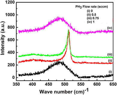 |
| | Fig. 1 Raman spectra of n type nc-Si:H films deposited at different PH3 flow rates. | |
Yue Kuo25 demonstrated the effect of SiH4 (1% PH3) flow rates on phosphorus doped n+ silicon films and observed that the volume fraction of microcrystalline phase in the film decreases with the increase in flow rates along with shifting of peak in Raman spectrum. Debajyoti Das et al.10 reported the overall crystallinity of the n type nc-Si network reduced from 78.5% to 51% at higher PH3 flow rates.
These films prepared at PH3 flow rates of 0.5 and 0.75 sccm have a sharp peak at 520 cm−1, corresponding to the transverse optic (TO) phonon vibration, which is due to the presence of nano-crystalline phase.26 With an increase in the PH3 flow rate beyond 0.75, the intensity of TO peak is decreased and broader. This is due to reduction in the crystalline volume fraction as the PH3 flow rate increased. From these results, it is observed that the addition of PH3 beyond limit in nc-Si:H network causes nano-crystalline to amorphous transition in the films. At zero doping level (no doping), the film is mostly amorphous while with subsequent inclusion of PH3 in the deposition process enhances the overall crystallinity. There is a reduction in crystalline volume fraction beyond 0.75 sccm and this is due to lattice distortion and more disordered atomic arrangement. The higher PH3 doping also does a change in structural properties of the material. Therefore, optimized PH3 concentration is essential for making thin films electronic devices.
The variation in structural morphology with respect to doping of n type nc-Si:H films is examined by X-ray diffraction pattern, revealed in Fig. 2(a). The low peak intensity was observed at zero doping in the film which reveals that the deposited film is dominantly amorphous in nature. However, with doping at 0.5 sccm transition in film structure observed in Raman results are also correlated with the emergence of sharp crystalline peak at 28° along 〈1 1 1〉 diffraction plane in XRD. The crystalline nature in doped samples are observed by the appearance of characteristic peaks corresponding to different diffraction planes 〈1 1 1〉 and 〈2 2 0〉 at 2θ ∼28° and 47°respectively. These results signify the formation of nanocrystalline silicon structure embedded in the silicon matrix. However, it has been observed that the intensity of the 〈1 1 1〉 plane peak at 28° is much higher than the intensity of the 〈2 2 0〉 peak, which indicates the preferential crystalline growth along the 〈1 1 1〉 crystallographic orientation. Though, with further increase in doping beyond 0.75 sccm less intensity peak shows reduction in crystalline nature and shifting towards amorphous. The average crystallite size (D) along with the 〈1 1 1〉 orientation in the nc-Si:H film has been calculated from full width at half maximum (FWHM) of the XRD peak using Debye Scherrer's formula27 where λ is the wavelength of X-ray radiation, β is full width at half maximum (FWHM) of XRD peak at diffraction angle θ.
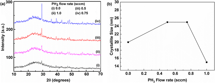 |
| | Fig. 2 (a) XRD spectra of PH3 doped n type nc-Si:H films deposited at different PH3 flow rates (b) variation in crystallite size with PH3 flow rates. | |
The variation in average crystallite size (D) with respect to PH3 doping is shown in Fig. 2(b). The 〈1 1 1〉 oriented nanocrystallite size ‘D’ reduced from ∼25 nm to ∼15 nm on increasing PH3 flow rates from 0.75 to 1 sccm. However from 0.5 to 0.75 sccm no change in size was observed. But initially the size increases from 20 nm to 25 nm at 0.0 to 0.5 sccm respectively due to introduction of dopant atoms. The reduction in nanocrystallite size with increase in doping might be induced amorphization in the crystalline structure. An elevated doping leads to the formation of P–Si–H clusters and disordered amorphous region generating voids between the crystalline matrix.28
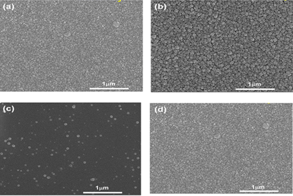
The plane view of field emission scanning electron microscope (FESEM) of n type nc-Si:H films is shown in Fig. 3(a–d). At elevated doping the distribution of crystalline grains and surrounding grain boundaries can be seen in Fig. 3(b and c). The smooth surface morphology of undoped and doped at 1 sccm in Fig. 3(a and d) respectively confirms the formation of reduced nature of crystallinity and noticeable reduction in grain size forming amorphous matrix. The small nano-sized crystallites are embedded in silicon matrix at doping of 0.5 and 0.75 sccm. The amorphous to crystalline transformation takes place at 0.5 sccm that is also confirmed with the help of Raman results. However, in Fig. 3(c) it is seen that grains are more or less of same size and distributed uniformly in the matrix.
 |
| | Fig. 3 Top view FESEM images of PH3 doped n type nc-Si:H films grown at different PH3 flow rates (a) 0.0 (b) 0.5 (c) 0.75 and (d) 1 sccm. | |
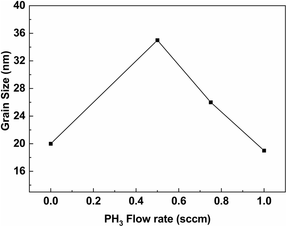
From the SEM analysis it is observed that grain size initially increases from 20 nm (at 0 sccm) to 35 nm (at 0.5 sccm) and then starts decreasing. Similar observations can be seen from the XRD results also. The variation in grain size (±5 nm) with respect to PH3 doping is shown in Fig. 4. The reduction in grain size with increase in doping from 0.75 to 1 sccm may be due to induced amorphization in the crystalline structure and formation of P–Si–H clusters and disordered amorphous region.28
 |
| | Fig. 4 Variation in the grain size due to increased PH3 flow rates. | |
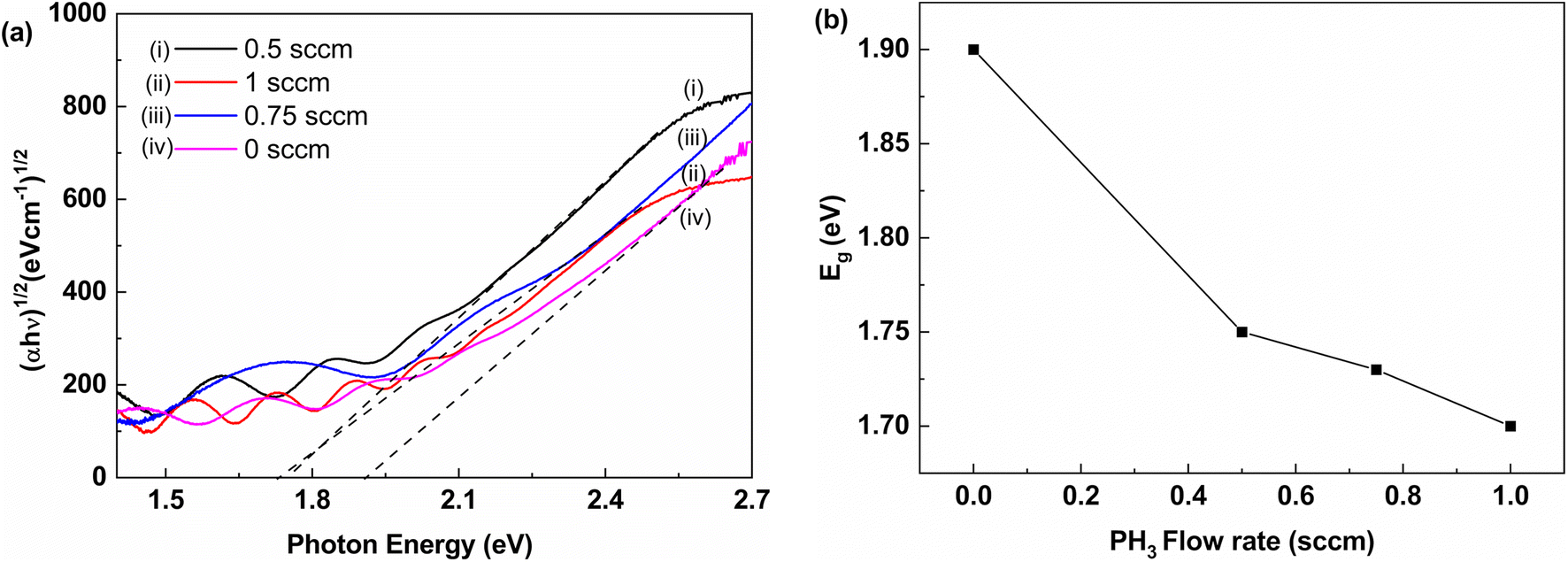
The change in optical bandgap (Eg) for undoped (0 sccm) and doped at 0.5, 0.75 and 1 sccm of n type nc-Si:H films was determined using the well-known Tauc's relation (αhν)1/2 = B(hν − Eg), where B stands for Tauc's constant and α is absorption coefficient as a function of photon energy hν, see Fig. 5(a) and (b).29,30 The absorption coefficient α was calculated from UV-visible absorbance data (see Fig. S2†).
 |
| | Fig. 5 (a) Tauc's plot of PH3 doped films (b) change in optical band gap (Eg) with PH3 flow rates. | |
From these results it has been found that the Eg decreases from 1.9 eV to 1.71 eV, on increasing PH3 flow rates from 0 to 1 sccm. The change in energy gap may be due to localized defects and accumulation of donor impurity atoms below conduction band leading to narrowing energy band gap.10,31 The reduction in crystalline volume fraction due to rise in PH3 flow rates may be attributed to decrease in optical band gap.32
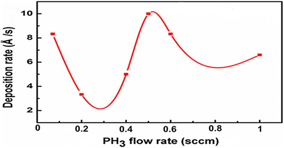
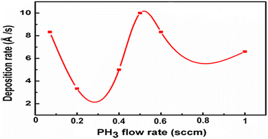
The change in deposition rate as a function of PH3 flow rates for n type nc-Si:H films is shown in Fig. 6. The deposition rate was calculated from the ratio of film thickness and deposition time. The film thickness was measured using a talystep surface profilometer. The deposition rate was ∼8.5 Å s−1 at ∼0.1 sccm PH3 flow rate. As the PH3 flow rate was further increased, the deposition rate decreased to minimum ∼2.2 Å s−1 for PH3 flow rate of 0.29 sccm. The increment in density of film not forming radicals and more hydrogen content may be the reason for initial decrease in deposition rate.
 |
| | Fig. 6 Variation of deposition rate as a function of PH3 flow rates for n type nc-Si:H films deposited by PECVD technique. | |
The maximum deposition rate ∼10 Å s−1 was achieved for films deposited at 0.5 sccm and beyond 0.5 sccm, the deposition rate decreased. The films were deposited using very high frequency (VHF > 50 MHz) at 20 W and hence the use of VHF results in increased density of precursors and high deposition rate. However beyond certain limit at high frequency the ion bombardment growing surface increases which results in reduction of crystalline growth. It is observed that deposition rate first decreases and then increases again with PH3 flow because with increase in pressure, the density of film forming precursor increases thus reducing mean free path for precursors in the plasma. For the application purpose, higher deposition rate is required with reduced processing time and cost.
The temperature dependent dark conductivity of doped and undoped film was measured from 300 to 477 Kelvin to elucidate electrical behavior. The conductivity of undoped film (at 0 sccm) increases on increasing temperature due to generation of more intrinsic charge carrier generation and hence leading to more intrinsic conductivity as shown in Fig. 7. But more variation in conductivity due to temperature of doped films is not observed from 300 to 477 Kelvin being temperature independent majority carriers. The dark conductivities are calculated from the relation
where ‘
V’ refers to voltage, ‘
I’ is current, ‘
T’ is thickness, ‘
W’ is width and
L is the distance between the electrodes. Furthermore, the variation in dark conductivity (
σD) and activation energy (
Ea) with respect to the PH
3 flow rates for the n type nc-Si:H films is shown in
Fig. 8. The logarithmic value of
σD with 1000/
T as presented in
Fig. 7 identified thermal activation type behaviour following the Arrhenius relation as described in
eqn (1), where
σ0 is the conductivity pre-exponential factor,
Ea is the activation energy and
kB is the Boltzmann constant and
T is temperature in Kelvin.
| |
 | (1) |
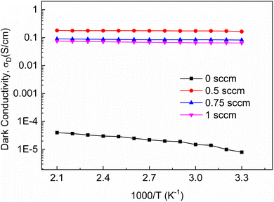 |
| | Fig. 7 Effect of temperature on dark conductivity (σD) for different PH3 flow rates. | |
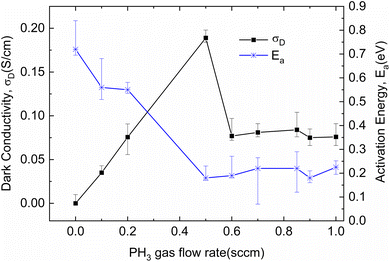 |
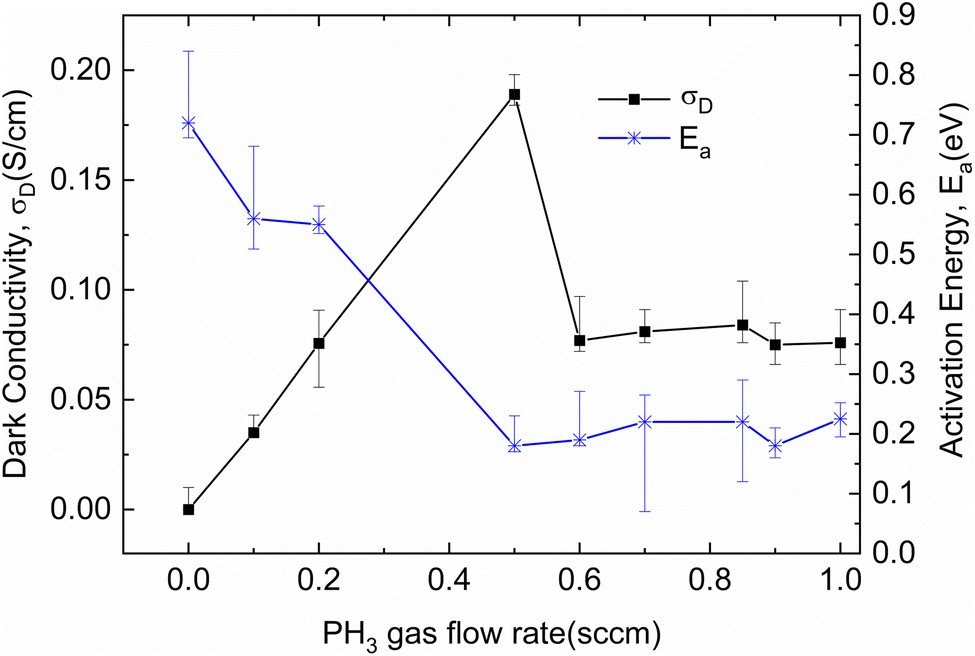
| | Fig. 8 Variation in dark conductivity (σD) and charge carrier activation energy (Ea) as a function of the PH3 flow rates. | |
As can be seen from Fig. 8, significant changes were observed in the dark conductivity (σD) and activation energy of films with different PH3 concentration. The mean value of σD and Ea with error bar was obtained from 5 different sample measurements. It has been observed that as the PH3 gas flow rate increases, the conductivity initially starts increasing and reaches a maximum value of 0.18 S cm−1 and then decreases to minimum 0.07 S cm−1. The initial increase in conductivity of nanocrystalline films is due to presence of large number of defects and impurities such as oxygen and nitrogen that are compensated by PH3 doping.33 This confirms that the PH3 doping compensates the defects and impurities grown in the material and therefore the film becomes n-type with improved conductivity. The room temperature σD was measured in the coplanar geometry by evaporating the Al contacts on the films using vacuum thermal evaporation. As shown in Fig. 8, for pure film, the dark conductivity and activation energy (Ea) is ∼10−5 S cm−1 and 700 meV respectively. When the PH3 flow rate is maintained at 0.2 sccm, the dark conductivity is increased to 0.072 S cm−1. With a further increase in the PH3 flow rates, the dark conductivity reaches a maximum value of 0.18 S cm−1 along with lowest Ea of 190 meV at 0.5 sccm. This may be due to shifting of Fermi level more close to conduction band edge resulting high conductivity and lowering activation energy.
Lucovsky et al.34 proposed a model to explain origin of reverse-Meyer–Neldel rule (MNR) phenomena which supports that the Fermi energy level moves in n type semiconductor above the bottom of conduction band in the crystalline phase and simultaneously it may shift more into the band tail states of the surrounding disordered amorphous regions. K. P. Chil et al.35 reported the highly degenerate microcrystalline phosphorus-doped silicon films grown by thermal LPCVD method and found the position of Fermi level inside the conduction band.
However, the conductivity is decreased further with increase in the PH3 flow rate beyond 0.75 sccm. The decrease in dark conductivity for higher PH3 concentration at 1 sccm may be due to reduction in crystallinity and more defect generation. Low angle XRD and Raman analysis also confirms the deterioration of crystallinity at 1 sccm as compared to 0.5 sccm. The deposition parameters used to develop the films are given in Table 1.
Table 1 Deposition parameters used for the fabrication of n-type nc-Si:H films by PECVD technique
| Process parameters |
Value |
| Base pressure |
3.8 × 10⁻⁶–4.1 × 10⁻⁶ torr |
| Deposition pressure |
0.25 torr |
| Gas flow rate |
|
| SiH4 |
4 sccm |
| PH3 |
0.0–1.0 sccm |
| Very high frequency (VHF) power |
20 Watt |
| Deposition time |
10 min |
| Substrate temperature |
200 °C |
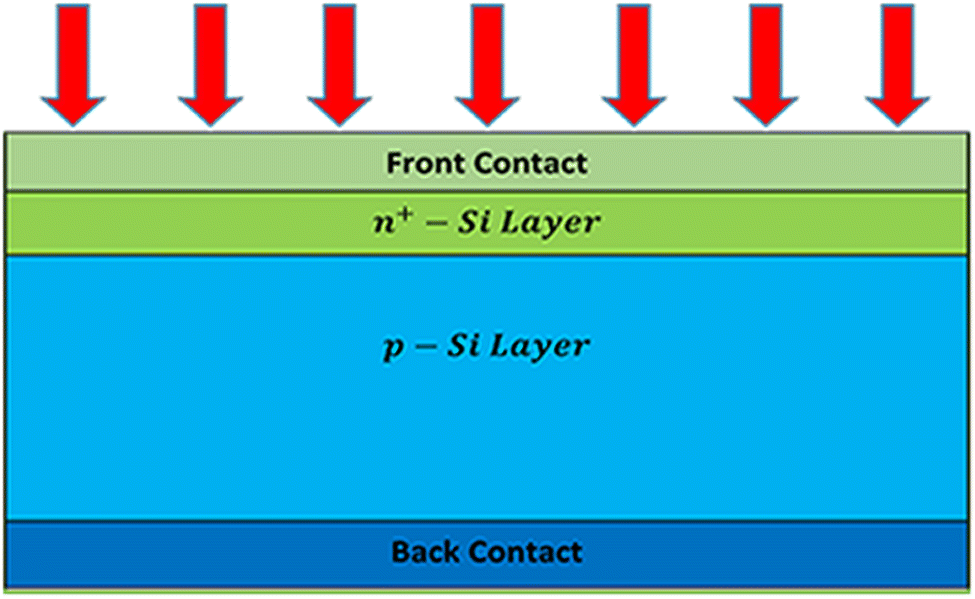
However for fabrication of solar cell, optimization for parameters is important. Crystalline silicon (c-Si) dominates the wafer-based solar cells while amorphous silicon (a-Si) plays a vital role in thin-film solar cells. In this theoretical work crystalline silicon p–n junction solar cell has been simulated using SCAP-1D simulation tool. The schematic of simulated structure of the solar cells is shown in Fig. 9.
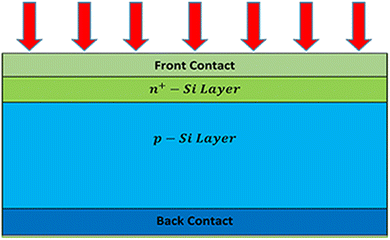 |
| | Fig. 9 Schematic structure of simulated pn junction solar cell. | |
The parameters required in the simulation such as initial thickness of n and p layer, charge carrier mobility, band gap, density of states etc. are taken from different published sources and input file given by SCAP software, as shown in Table 2.
Table 2 Optical and electrical input parameters used for device simulation
| Parameters |
p layer |
n layer |
| Initial thickness (nm) |
300![[thin space (1/6-em)]](https://www.rsc.org/images/entities/char_2009.gif) 000 000 |
100 |
| Bandgap (eV) |
1.12 |
1.12 |
| Electron affinity (eV) |
4.050 |
4.050 |
| Dielectric permittivity (relative) |
11.90 |
11.90 |
| CB effective DOS (cm−3) |
2.8 × 10¹⁹ |
2.8 × 10¹⁹ |
| VB effective DOS (cm−3) |
1.04 × 10¹⁹ |
1.04 × 10¹⁹ |
| Electron thermal velocity (cm s−1) |
2.3 × 10⁷ |
2.3 × 10⁷ |
| Hole thermal velocity (cm s−1) |
1.65 × 10⁷ |
1.65 × 10⁷ |
| Electron mobility (cm2 V−1 s−1) |
1.5 × 10³ |
1.5 × 10³ |
| Hole mobility (cm2 V−1 s−1) |
4.5 × 10² |
4.5 × 10² |
| ND (donor density) (cm−3) |
1010 |
1019 |
| NA (acceptor density) (cm−3) |
1015 |
1010 |
| Density of defects |
1013 |
1013 |
3.1 Effect of layer thickness on output parameters
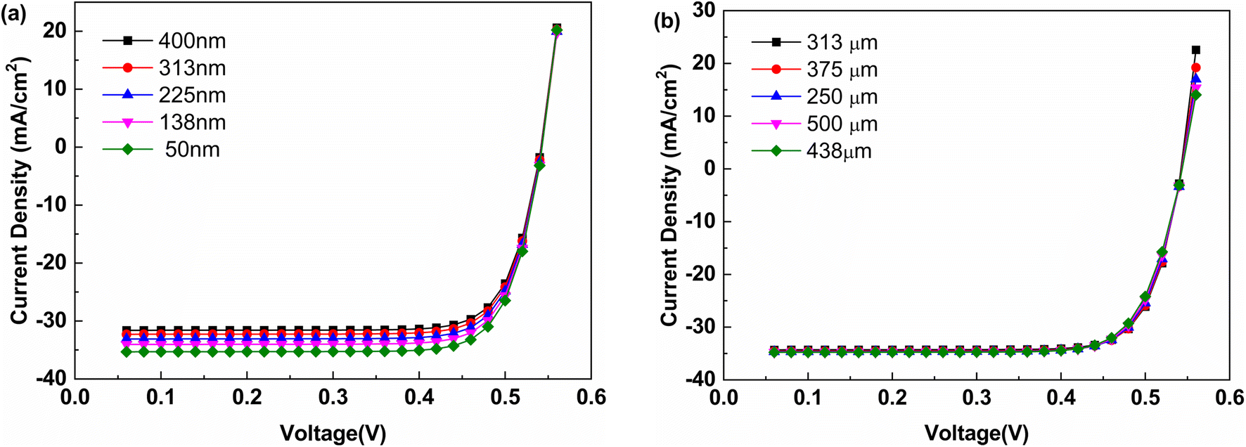
The layer thickness is one of the major parameters in the solar cell configuration. The thickness variation causes significant effect on the device output VOC, JSC, FF and PCE. In order to optimize the thickness of the n and p layer, it has been varied from 50 nm to 400 nm and 250 to 500 μm respectively. The effect of thickness on JV characteristics is shown in Fig. 10(a) and (b) for n type and p type respectively. It can be seen that as there is increase in the thickness of n type layer from its initial value of 50 nm, the PCE starts decreasing. This is due to more front surface recombination in n type layer and near p–n junction. This leads to reduction in current density because less number of charge carriers are collected to their respective electrodes. While on varying thickness in p layer, no major change in JV curve is observed.
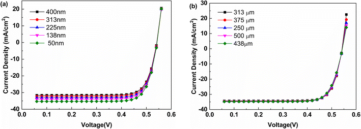 |
| | Fig. 10 Effect of thickness variation in (a) n type layer (b) p type layer on JV characteristics. | |
These results are also supported by external quantum efficiency (EQE) curves. For n type layer, at lower wavelength the % of EQE is better at 50 nm while it decreases on increasing thickness. At lower wavelength due to front surface recombination and thermalization losses the EQE decreases. On the other hand, for p type layer there is no effect of thickness on EQE and JV. The EQE results are shown in Fig. 11(a) and (b) for n type and p type respectively.
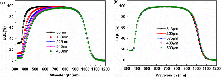 |
| | Fig. 11 Impact of thickness variation in (a) n type layer (b) p type layer on EQE. | |
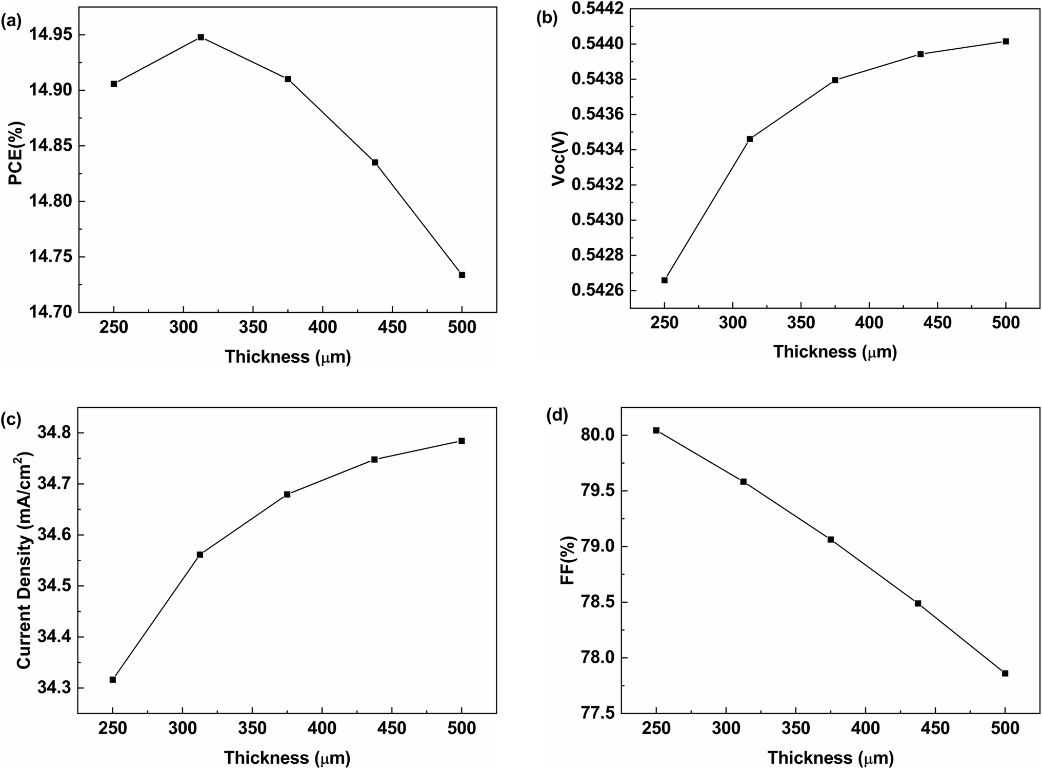
As the n type emitter layer thickness increases, the PCE decreases due to reduction in current density and dip in EQE. However, there is no major variation is observed in VOC but slight change may be due to front surface recombination. The effect of thickness on output parameters in n type layer are shown in Fig. 12(a–d). The effect of thickness variation in n type and p type layer on solar cell parameters is given in Tables 3 and 4 respectively.
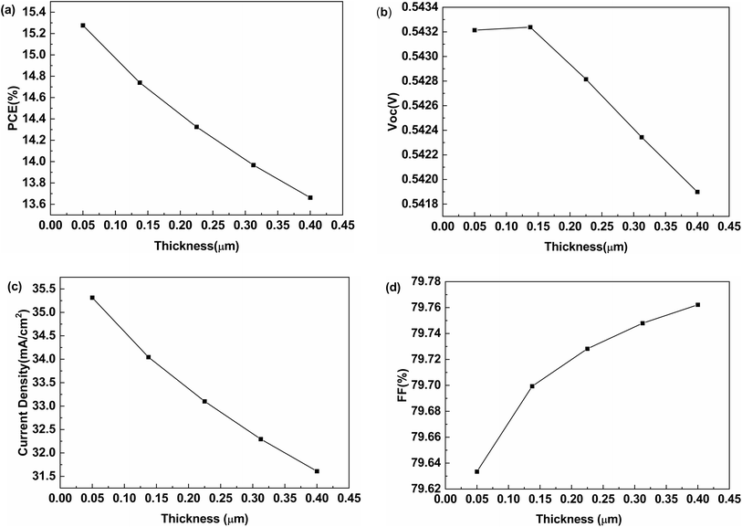 |
| | Fig. 12 Impact of thickness variation in n-type layer on output parameters (a) PCE (b) VOC (c) current density (d) FF. | |
Table 3 Effect of n-type layer thickness variation on solar cell parameters
| Thickness (nm) |
JSC (mA cm−2) |
VOC (V) |
FF% |
PCE% |
| 50 |
35.31481 |
0.54321 |
79.63348 |
15.27648 |
| 138 |
34.04482 |
0.54324 |
79.69935 |
14.73996 |
| 225 |
33.10142 |
0.54282 |
79.72825 |
14.32553 |
| 313 |
32.29507 |
0.54234 |
79.74795 |
13.96787 |
| 400 |
31.60949 |
0.5419 |
79.76215 |
13.66258 |
Table 4 Effect of p type layer thickness variation on solar cell parameters
| Thickness (μm) |
JSC (mA cm−2) |
VOC (V) |
FF% |
PCE% |
| 250 |
34.31629 |
0.54266 |
80.04386 |
14.90581 |
| 313 |
34.5614 |
0.54346 |
79.5832 |
14.94792 |
| 375 |
34.67956 |
0.54379 |
79.06316 |
14.91019 |
| 438 |
34.74799 |
0.54394 |
78.48913 |
14.83517 |
| 500 |
34.78447 |
0.54402 |
77.86074 |
14.73382 |
The thickness of p type layer is varied from 250 to 500 μm but no major change in output parameters has been observed in this range. The results are shown in Fig. 13(a–d).
 |
| | Fig. 13 Impact of thickness variation in p type layer on output parameters (a) PCE (b) VOC (c) current density (d) FF. | |
3.2 Effect of defect density on output parameters
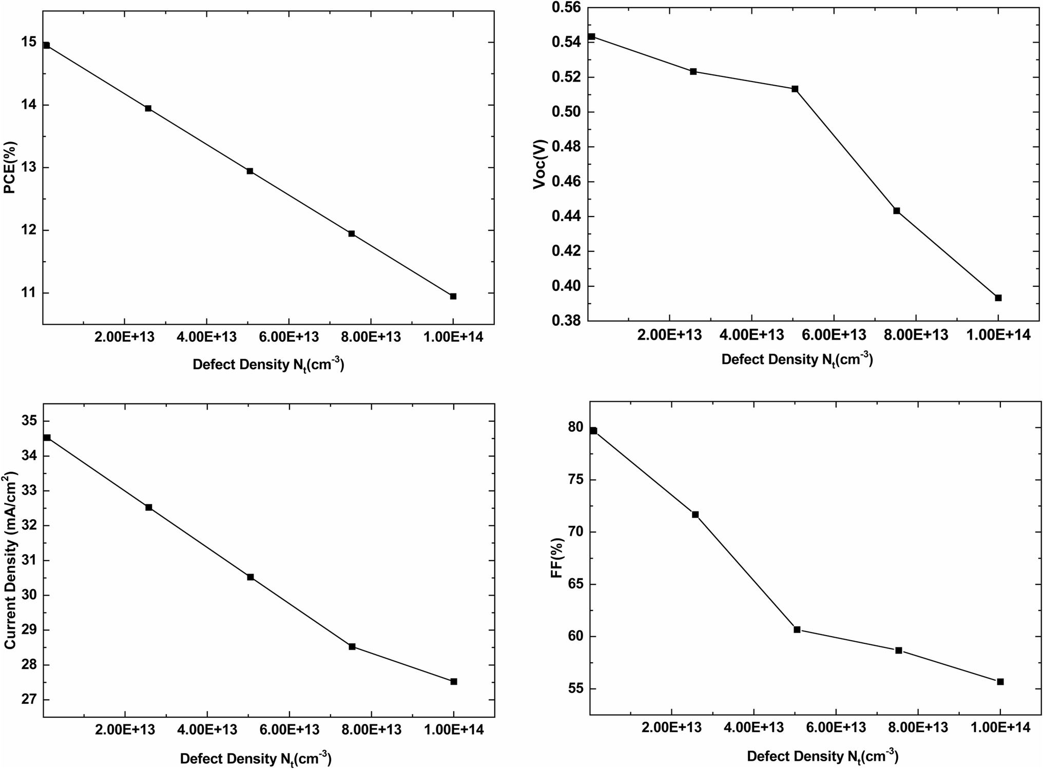
The defect density (Nt) has a significant effect on the performance of the solar cell parameters. Higher level of defect density reduces the carrier life time and increases the recombination. As the defects density increases, the recombination increases and carrier mobility decreases due to traps and hence all output parameters decreases. The effect of defect density variation in n type layer is shown in Fig. 14 in which all output parameters decreases on increasing defect density. The defect density is varied from 1013 to 1014 cm−3 in n type layer.
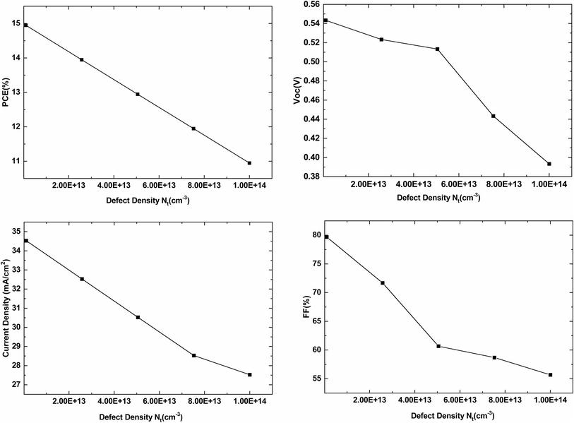 |
| | Fig. 14 Effect of defect density variation in n-type layer on output parameters. | |
Similarly, the effect of defect density variation in p type layer is shown in Fig. 15 in which all the output parameters decreases on increasing defect density. The defect density is varied from 1013 to 1016 cm−3 in p type layer. The effect of defect density variation in n type and p type layer on output parameters is given in Tables 5 and 6 respectively.
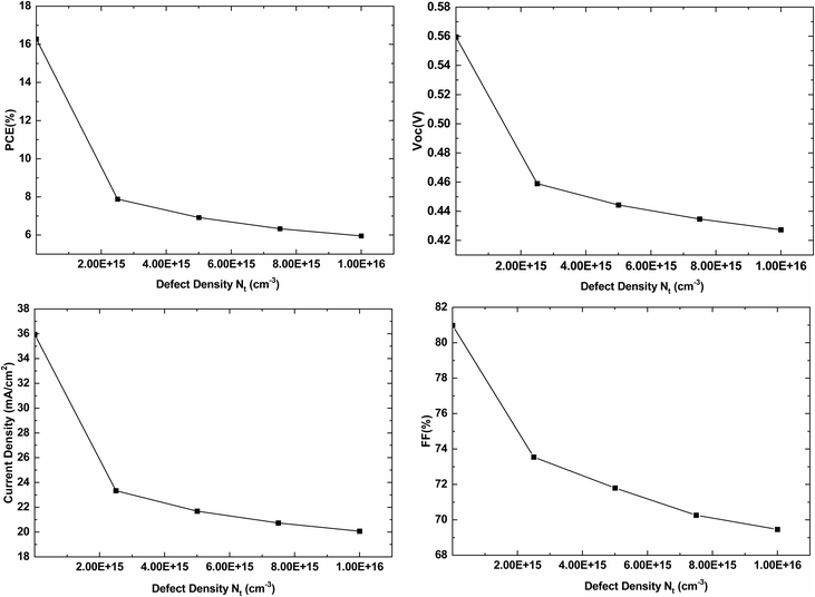 |
| | Fig. 15 Effect of defect density variation in p-type layer on output parameters. | |
Table 5 Effect of defect density variation in n type layer on output parameters
| Defect density (cm−3) |
JSC (mA cm−2) |
VOC (V) |
FF% |
PCE% |
| 1.00 × 10¹³ |
34.5275 |
0.54335 |
79.68022 |
14.94853 |
| 2.58 × 10¹³ |
32.5275 |
0.52335 |
71.68022 |
13.94853 |
| 5.05 × 10¹³ |
30.5275 |
0.51335 |
60.68022 |
12.94853 |
| 7.53 × 10¹³ |
28.5275 |
0.44335 |
58.68022 |
11.94853 |
| 1.00 × 10¹⁴ |
27.5275 |
0.39335 |
55.68022 |
10.94853 |
Table 6 Effect of defect density variation in p type layer on output parameters
| Defect density (cm−3) |
JSC (mA cm−2) |
VOC (V) |
FF% |
PCE% |
| 1.00 × 10¹³ |
35.94573 |
0.55954 |
80.97943 |
16.28738 |
| 2.50 × 10¹⁵ |
23.34534 |
0.45893 |
73.54753 |
7.87988 |
| 5.00 × 10¹⁵ |
21.68631 |
0.44431 |
71.79455 |
6.9177 |
| 7.50 × 10¹⁵ |
20.73422 |
0.4347 |
70.26206 |
6.33288 |
| 1.00 × 10¹⁶ |
20.07179 |
0.42737 |
69.46169 |
5.95844 |
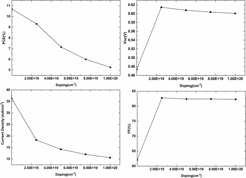
3.3 Effect of doping on output parameters
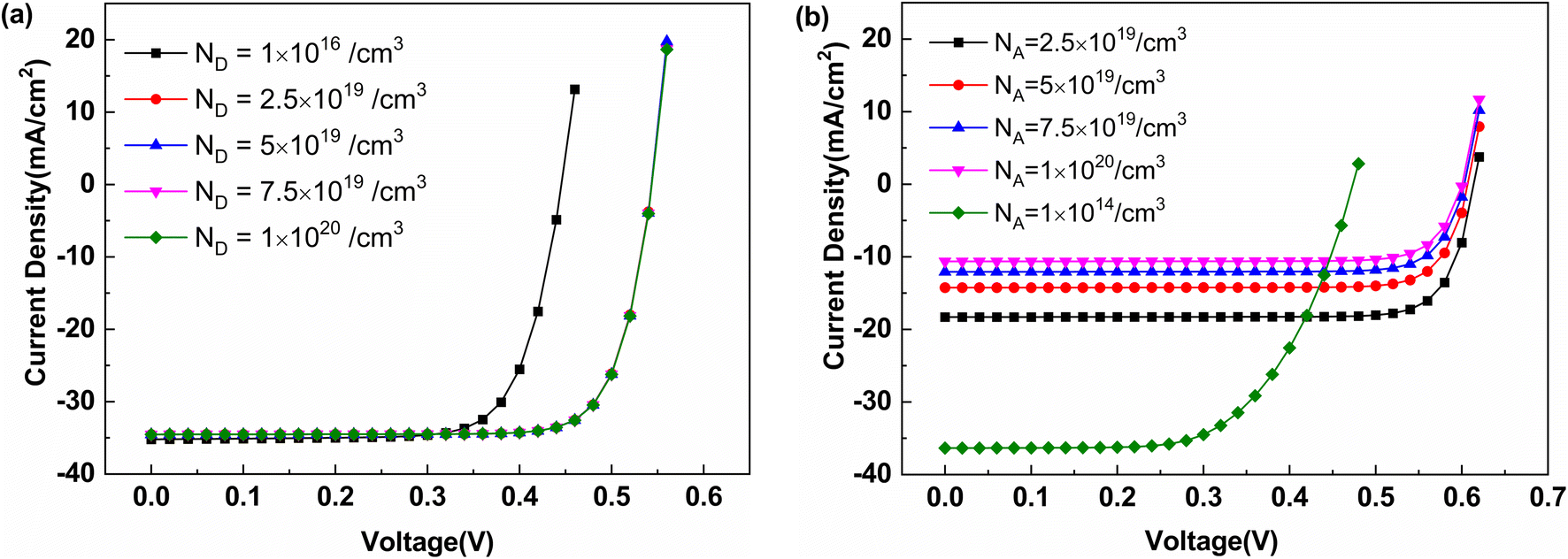
The output performance of the crystalline silicon solar cells is highly influenced by the quality and structure of the layers. The doping concentration plays an important role in obtaining effective output of the device. To measure the effect of doping on the performance of the solar cell, the donor and acceptor concentration is varied from 1 × 10¹⁶ to 1 × 1020 cm−3 in n type layer and 1 × 10¹⁴ to 1 × 1020 cm−3 in p type layer respectively. It is quite clear from Fig. 16 that output parameters are constant after doping of 2.5 × 1019 cm−3. Heavy doping beyond limit in a semiconductor leads to more recombination because of too many scattering centers and even more change in structural nature that has been confirmed with the help of Raman and XRD data also. These changes effects charge transport mechanism in a semiconductor. The effects of doping of acceptor impurity atoms in p layer on output parameters are shown in Fig. 17. The current density and PCE decreases on increasing doping. The effects of doping in p layer are observed more than n layer. The change in EQE curve for n type layer is less as shown in Fig. 18(a) but for p type layer more variation in EQE results is obtained, as shown in Fig. 18(b).The current density variation due to doping in n and p layer is shown in Fig. 19(a) and (b) respectively. On increasing doping in p layer current density decreases as shown in Fig. 19(b) and % of EQE also decreases. The optimum doping for p layer is 1 × 10¹⁴ and beyond this current density decreases which may be due to back surface recombination and lack of absorbed photon quantity. The effect of doping in n-type and p-type layer on output parameters is given in Tables 7 and 8 respectively.
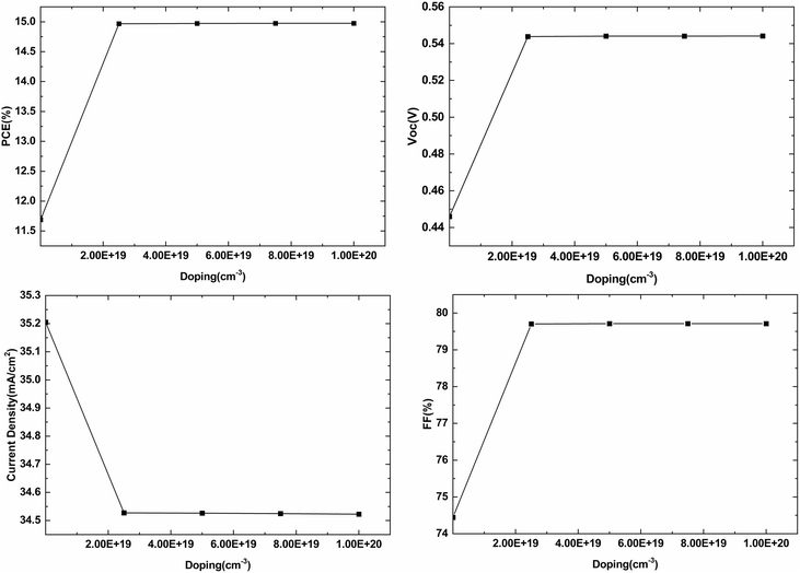 |
| | Fig. 16 Effect of doping in n-type layer on output parameters. | |
 |
| | Fig. 17 Effect of doping in p-type layer on output parameters. | |
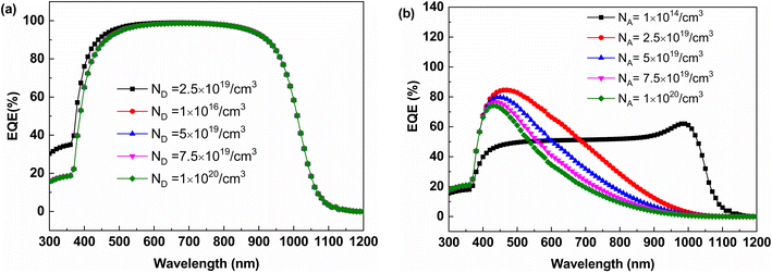 |
| | Fig. 18 Effect of doping in (a) n type layer (b) p type layer on EQE. | |
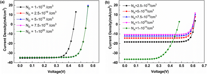 |
| | Fig. 19 Effect of doping in (a) n type layer (b) p type layer on JV characteristics. | |
Table 7 Effect of doping in n-type layer on output parameters
| Doping (cm−3) |
JSC (mA cm−2) |
VOC (V) |
FF% |
PCE% |
| 1.00 × 10¹⁶ |
35.20517 |
0.44602 |
74.44422 |
11.68944 |
| 2.50 × 10¹⁹ |
34.52734 |
0.54389 |
79.7035 |
14.9676 |
| 5.00 × 10¹⁹ |
34.52651 |
0.54407 |
79.71079 |
14.97359 |
| 7.50 × 10¹⁹ |
34.52497 |
0.54413 |
79.71319 |
14.97502 |
| 1.00 × 10²⁰ |
34.52281 |
0.54416 |
79.7144 |
14.97511 |
Table 8 Effect of doping in p-type layer on output parameters
| Doping (cm−3) |
JSC (mA cm−2) |
VOC (V) |
FF% |
PCE% |
| 1.00 × 10¹⁴ |
36.34676 |
0.47377 |
62.12877 |
10.69867 |
| 2.50 × 10¹⁹ |
18.29967 |
0.61468 |
82.78289 |
9.31176 |
| 5.00 × 10¹⁹ |
14.2573 |
0.60793 |
82.42996 |
7.14454 |
| 7.50 × 10¹⁹ |
12.0726 |
0.60373 |
82.4101 |
6.00649 |
| 1.00 × 10²⁰ |
10.64165 |
0.60065 |
82.30128 |
5.26061 |
4 Conclusion
Phosphorous doped n type nano/micro crystalline silicon films are prepared at substrate temperature of 200 °C by varying PH3 flow rates from 0 to 1 sccm using PECVD method. At higher flow rate approximately 1 sccm, crystalline nature of film decreases inducing miniaturization of 〈1 1 1〉 oriented grains. The doping of phosphorous atoms in silicon network at 0.5 sccm contributes plenty of free electrons resulting in high dark conductivity and crystallinity. At higher doping level, mobility of charge carriers decreases due to generation of defects below the conduction band edge, resulting in lower dark conductivity (∼at 1 sccm). The novelty of the present work lies in developing nano/micro crystalline thin film at 200 °C by doping of phosphorus atoms using PECVD technique. The optimum optical and structural properties, significant crystallinity, good electrical conductivity has been obtained at doping of 0.5 sccm. These films may find application in heterojunction solar cells as an emitter layer. Further crystalline silicon (c-Si) based simple p–n junction solar cell is simulated using SCAP-1D tool to observe the effect of layer thickness and doping density on solar cell parameters.
Data availability
The data supporting this paper have been included as part of the ESI.†
Author contributions
All authors contributed in experiments and theoretical results analysis. Further they all supported to manuscript preparation and revision.
Conflicts of interest
The authors declare that they have no conflicts of interest.
Acknowledgements
The authors are thankful to Haryana State Council for Science Innovation and Technology (HSCSIT) for providing financial assistance under the R & D research project grant (HSCSIT/R&D/2022/2657 dated 10/10/2022). Authors are also very thankful to Marc Burgelman, Department of Electronics and Information Systems at the University of Gent, Belgium, for providing SCAPS simulation software.
References
- D. Das and L. Karmakar, Autogenic single p/n-junction solar cells from black-Si nano-grass structures of p-to-n type self-converted electronic configuration, Nanoscale, 2020, 12, 15371–15382 RSC.
- D. Das and L. Karmakar, Optimization of Si Doping in ZnO Thin Films and Fabrication of n-ZnO:Si/p-Si Heterojunction Solar Cells, J. Alloys Compd., 2020, 824, 153902 CrossRef CAS.
- J. Haschke, et al., Silicon Heterojunction Solar Cells: Recent Technological Development and Practical Aspects – from Lab to Industry, Sol. Energy Mater. Sol. Cells, 2018, 187, 140–153 CrossRef CAS.
- A. Richter, et al., Versatility of Doped Nanocrystalline Silicon Oxide for Applications in Silicon Thin-film and Heterojunction Solar Cells, Sol. Energy Mater. Sol. Cells, 2018, 174, 196–201 CrossRef CAS.
- R. Street, Technology and Application of Amorphous Silicon, Springer Verlag, New York, 2000 Search PubMed.
- M. Sharma, et al., Nanocrystalline Silicon Thin Film Growth and Application for Silicon Heterojunction Solar Cells: A Short Review, Nanoscale Adv., 2021, 3, 3373–3383 RSC.
- A. Shah, et al., Material and Solar Cell Research in Microcrystalline Silicon, Sol. Energy Mater. Sol. Cells, 2003, 78, 469–491 CrossRef CAS.
- K. Yamamoto and et al., Novel hybrid thin film silicon solar cell and module, 3rd World Conference on Photovoltaic Energy Conversion, Proceedings of Osaka, Japan, 2003, vol. 3, pp. 2789–2792 Search PubMed.
- H. Zhou, et al., Dilution Effect of Ar/H2 on the Microstructures and Photovoltaic Properties of nc-Si:H Deposited in Low Frequency Inductively Coupled Plasma, J. Appl. Phys., 2011, 110, 023517 CrossRef.
- D. Das and C. M. Patra, Superior Phosphorous Doping in Nanocrystalline Silicon Thin Films and Their Application as Emitter Layers in Silicon Heterojunction Solar Cells, Energy Fuels, 2023, 37(8), 6062–6077 CrossRef CAS.
- S. Juneja, et al., Highly Conductive Boron Doped Micro/nanocrystalline Silicon Thin Films Deposited by VHF-PECVD for Solar Cell Applications, J. Alloys Compd., 2015, 643, 94–99 CrossRef CAS.
- S. E. Whibi, et al., Optimized nc-Si:H thin films with enhanced optoelectronic properties prepared by micro-waves PECVD used as an effective silicon surface passivation layer, J. Mater. Sci.: Mater. Electron., 2019, 30, 2351–2359 CrossRef.
- P. Sharma, et al., Nanocrystalline Silicon Thin Film Prepared by E-beam Evaporation for Display Application, J. Mater. Sci.: Mater. Electron., 2017, 28, 3891–3896 CrossRef CAS.
- I. Y. Y. Bu, A. J. Flewitt and W. I. Miline, Nanocrystalline Silicon Thin Films Fabricated at 80 °C by Using Electron Cyclotron Resonance Chemical Vapor Deposition, Plasma Sci. Technol., 2010, 12, 608–613 CrossRef CAS.
- R. Karmouch, Silicon Nanocrystals: From Synthesis to Applications, Int. J. Appl. Sci. Eng. Res., 2016, 7(12), 1498–1526 Search PubMed.
- A. Kherodia, V. Kheraj and A. K. Panchal, Effects of Hydrogen-Dilution on Opto-Structural Properties of Hot-wire CVD Grown a-Si:H/nc-Si:H Multilayer for Photovoltaics, Silicon, 2018, 10, 1475–1485 CrossRef CAS.
- R. Tripathi, et al., Study on nanocrystalline silicon thin films grown by the filtered cathodic vacuum arc technique using boron doped solid silicon for fast photo detectors, J. Taiwan Inst. Chem. Eng., 2018, 86, 185–191 CrossRef CAS.
- F. ZeudmiSahraoui, et al., Optical, structural evolution and surface morphology studies of hydrogenated silicon films synthesized by RF-magnetron sputtering: effects of pressure and radio frequency power at low temperature, Optik, 2018, 168, 65–76 CrossRef CAS.
- H. Chen and W. Z. Shen, Optical Characterization of Boron-doped Nanocrystalline Si:H Thin Films, Surf. Coat. Technol., 2005, 198, 98–103 CrossRef CAS.
- K. Yamamoto, et al., Cost Effective and High-performance Thin Film Si Solar Cell Towards the 21st Century, Sol. Energy Mater. Sol. Cells, 2001, 66, 117–125 CrossRef CAS.
- A. V. Shah, et al., Material and Solar Cell Research in Microcrystalline Silicon, Sol. Energy Mater. Sol. Cells, 2003, 78, 469–491 CrossRef CAS.
- A. Shah, et al., Towards Very Low-cost Mass Production of Thin-film Silicon Photovoltaic (PV) Solar Modules on Glass, Thin Solid Films, 2006, 502, 292–299 CrossRef CAS.
- W. Abdelaziz, et al., Possible Efficiency Boosting of Non-fullerene Acceptor Solar Cell Using Device Simulation, Opt. Mater., 2019, 91, 239–245 CrossRef CAS.
- T. Minemoto and M. Murata, Impact of Work Function of Back Contact of Perovskite Solar Cells Without Hole Transport Material Analyzed by Device Simulation, Curr. Appl. Phys., 2014, 14(11), 1428–1433 CrossRef.
- Y. Kuo, Doping gas
effects on plasma enhanced chemical vapor deposition on heavily phosphorus-doped n+ silicon film, Appl. Phys. Lett., 1997, 71, 2821–2823 CrossRef CAS.
- S. Juneja and S. Kumar, Effect of Power on Crystallinity and Opto-electronic Properties of Silicon Thin Films Grown Using VHF PECVD Process, Silicon, 2021, 13, 3927–3940 CrossRef CAS.
- B. D. Cullity, Elements of X-Ray Diffraction, Addison Wesley, Reading, MA, 1978, p. 283 Search PubMed.
- M. Birkholz, et al., Amorphous-crystalline Phase Transition During the Growth of Thin Films: The Case of Microcrystalline Silicon, Phys. Rev. B, 2001, 64, 085402 CrossRef.
- Y. He, et al., The Structure and Properties of Nanosize Crystalline Silicon Films, J. Appl. Phys., 1994, 75, 797 CrossRef CAS.
- R. A. Street, Hydrogenated Amorphous Silicon, Cambridge University Press, 1991 Search PubMed.
- M. K. Abdel-Latif, et al., Effect of doping on the structural, optical and electrical properties of La-doped ZnO thin films, J. Mater. Sci.: Mater. Electron., 2023, 34, 254 CrossRef CAS.
- B. Gabhale, et al., Effect of Phosphine Gas Conditions on Structural, Optical and Electrical Properties of Nc-Si:H Films Deposited by Cat-CVD Method, ES Materials & Manufacturing, 2020, 10, 52–59 Search PubMed.
- S. Jadkar, et al., Synthesis of Highly Conductive Boron-doped p-type Hydrogenated Microcrystalline Silicon (μc-Si:H) by a Hot-wire Chemical Vapor Deposition (HWCVD) Technique, Sol. Energy Mater. Sol. Cells, 2000, 64, 333–346 CrossRef CAS.
- G. Lucovsky, et al., An application of the statistical shift model to the inverted Meyer–Neldel, MN relationship in heavily-doped microcrystalline Si, μc-Si, J. Non-Cryst. Solids, 1993, 164–166, 973–976 CrossRef CAS.
- K. P. Chil, et al., Electronic transport in amorphous and microcrystalline phosphorus-doped silicon films prepared by thermal LPCVD, Philos. Mag. B, 1990, 61, 377–391 Search PubMed.
|
| This journal is © The Royal Society of Chemistry 2024 |
Click here to see how this site uses Cookies. View our privacy policy here. 
 Open Access Article
 This Open Access Article is licensed under a Creative Commons Attribution-Non Commercial 3.0 Unported Licence
 a,
Sucheta Juneja*b,
Shiv Kumar Dixit
a,
Sucheta Juneja*b,
Shiv Kumar Dixit