
 Open Access Article
 This Open Access Article is licensed under a Creative Commons Attribution-Non Commercial 3.0 Unported Licence
Vacancy-and doping-mediated electronic and magnetic properties of PtSSe monolayer towards optoelectronic and spintronic applications†
Duy Khanh Nguyen ab,
R. Ponce-Pérezc,
J. Guerrero-Sanchezc and
D. M. Hoat*de
ab,
R. Ponce-Pérezc,
J. Guerrero-Sanchezc and
D. M. Hoat*de
aLaboratory for Computational Physics, Institute for Computational Science and Artificial Intelligence, Van Lang University, Ho Chi Minh City, Vietnam. E-mail: khanh.nguyenduy@vlu.edu.vn
bFaculty of Mechanical – Electrical and Computer Engineering, School of Technology, Van Lang University, Ho Chi Minh City, Vietnam
cUniversidad Nacional Autónoma de México, Centro de Nanociencias y Nanotecnología, Apartado Postal 14, Código Postal 22800, Ensenada, Baja California, Mexico
dInstitute of Theoretical and Applied Research, Duy Tan University, Ha Noi 100000, Viet Nam. E-mail: dominhhoat@duytan.edu.vn
eFaculty of Natural Sciences, Duy Tan University, Da Nang 550000, Viet Nam
First published on 14th June 2024
Abstract
Developing new multifunctional two-dimensional (2D) materials with two or more functions has been one of the main tasks of materials scientists. In this work, defect engineering is explored to functionalize PtSSe monolayer with feature-rich electronic and magnetic properties. Pristine monolayer is a non-magnetic semiconductor 2D material with a band gap of 1.52(2.31) eV obtained from PBE(HSE06)-based calculations. Upon creating single Pt vacancy, the half-metallic property is induced in PtSSe monolayer with a total magnetic moment of 4.00 μB. Herein, magnetism is originated mainly from S and Se atoms around the defect site. In contrast, single S and Se vacancies preserve the non-magnetic nature. However, the band gap suffers of considerable reduction of the order of 67.11% and 48.68%, respectively. The half-metallicity emerges also upon doping with alkali metals (Li and Na) with total magnetic moment of 1.00 μB, while alkaline earth impurities (Be and Mg) make new diluted magnetic semiconductor materials from PtSSe monolayer with total magnetic moment of 2.00 μB. In these cases, magnetic properties are produced mainly by Se atoms closest to the doping site. In addition, doping with P and As atoms at chalcogen sites is also investigated. Except for the half-metallic AsSe system (As doping at Se site), the diluted magnetic semiconductor behavior is obtained in the remaining cases. Spin density results indicate key role of the VA-group impurities in magnetizing PtSSe monolayer. In these cases, total magnetic moments between 0.99 and 1.00 μB are obtained. Further Bader charge analysis implies the charge loser role of all impurities that transfer charge to the host monolayer. Results presented in this work may suggest promises of the defected and doped Janus PtSSe structures for optoelectronic and spintronic applications.
I. Introduction
Since the first successful isolation of graphene from graphite by Novoselov et al.,1 extensive theoretical and experimental investigations have asserted its intriguing physical, chemical, and mechanical properties that are quite different from and superior than those of graphite. For instance, graphene has a high electron mobility (∼15.000 cm2 V−1 s−1), high absorption rate about 2.3% of incident light, high mechanical stability - a hundred times stronger than steel,2,3 among others. The graphene band structure exhibits a direct point with linear dispersion at K point, where the valence band and conduction band meet. Practically, this zero-gap feature hinders considerably the efficiency of graphene when it is applied in electronic nanodevices.4 Although the graphene band gap can be opened by different methods as surface functionalization5,6 and cutting edges,7,8 it is very important to search for new semiconductor two-dimensional (2D) alternatives. So far, research efforts have conducted to the discovery of a large variety of 2D materials, which can be prepared in experiments by either top-down method (exfoliation from layered bulk structures)9,10 or bottom-up method (deposition growth from precursors).11,12 The discovered 2D materials hold great potential for catalysis,13,14 optoelectronics and electronics,15,16 photonics,17,18 energy conversion and storage,19,20 environmental and biomedical applications,21,22 spintronics,23,24 among others.As one of the big and relevant 2D materials family, transition metal dichalcogenides (TMDs) have gained special research attention.25 With a 1![[thin space (1/6-em)]](https://www.rsc.org/images/entities/char_2009.gif) :2 stoichiometry and chemical formula MX2 (M = transition metals; X = chalcogen atoms), TMDs structure is formed by sandwiching one M atomic sublayer between two X atomic sublayers. Initially, first structures based on VIB transition metals (M = Mo and W) were studied. These 2D structures exhibit semiconductor nature with relatively large energy gaps.26 Moreover, other intriguing properties have been also characterized including good environmental stability, flexibility, and tunable electronic band gap, and effective properties modification.27,28 2D MoX2 and WX2 structures have been explored as potential materials for flexible photonics,29,30 thermoelectrics,31,32 electronics,33,34 and light emissions,35,36 and so on. From the sandwiched structure, a new family called “Janus” structure MXY (X ≠ Y) have emerged with the discovery of MoSSe monolayer by either substituting S sublayer in MoS2 by Se sublayer or Se sublayer by S sublayer.37,38
:2 stoichiometry and chemical formula MX2 (M = transition metals; X = chalcogen atoms), TMDs structure is formed by sandwiching one M atomic sublayer between two X atomic sublayers. Initially, first structures based on VIB transition metals (M = Mo and W) were studied. These 2D structures exhibit semiconductor nature with relatively large energy gaps.26 Moreover, other intriguing properties have been also characterized including good environmental stability, flexibility, and tunable electronic band gap, and effective properties modification.27,28 2D MoX2 and WX2 structures have been explored as potential materials for flexible photonics,29,30 thermoelectrics,31,32 electronics,33,34 and light emissions,35,36 and so on. From the sandwiched structure, a new family called “Janus” structure MXY (X ≠ Y) have emerged with the discovery of MoSSe monolayer by either substituting S sublayer in MoS2 by Se sublayer or Se sublayer by S sublayer.37,38
Following the success of 2D TMDs, noble metals dichalcogenides have been also investigated by the worldwide research groups. For instance, Wang et al.39 have realized the epitaxial growth of high-quality single-crystal PtSe2 monolayer by direct selenization of Pt. Characterizations assert its semiconductor nature that is different from the metallic bulk counterpart. A combined experimental and theoretical investigation on the layer-dependent PtS2 monolayer properties has been carried out by Zhao et al.40 Results indicate a drastic band gap reduction from monolayer (1.6 eV) to bulk counterpart (0.25 eV), which can be attributed to the strong interlayer interactions of S-pz state. As an effective method to tune the PtS2 and PtSe2 monolayers properties, the formation of Janus structure PtSSe monolayer have been also studied. Various investigations have explored Janus PtSSe monolayer as promising 2D candidate for thermoelectrics,41 photocatalysis for water splitting,42 gas sensing,43,44 among others.
Recently, research interests have been focused on developing multifunctional 2D materials with two or more promising functions, which requires the artificial induction of novel feature-rich properties. In this regard, the magnetism engineering in 2D materials towards spintronic applications can be mentioned as a representative example. Generally, most of 2D materials are intrinsically non-magnetic, except for various transition metal containing members.45,46 Therefore, inducing significant magnetism along with feature-rich electronic properties plays a key role in order to make new spintronic materials. To the best of our knowledge, the exploration of Janus PtSSe monolayer as 2D spintronic platform has no been treated well, so far. In this work, our main aim is explore efficient magnetism engineering in Janus PtSSe monolayer through lattice defects, including vacancy and doping approach. The electronic and magnetic properties of Janus PtSSe monolayer effected by defects are analyzed in details by the spin-polarized band structure and projected density of states, Bader charge analysis, spin density, and magnetic moments. It is anticipated that Pt vacancy and doping (with P and As at chalcogen sites; with Al and Ga at Pt site) conduct to significant monolayer magnetization, meanwhile the effective band gap tuning can be achieved by chalcogen vacancies and doping with Be and Mg at Pt site. Results may suggest efficient approaches to effectively functionalize Janus PtSSe monolayer for optoelectronic and spintronic applications.
II. Computational details
On the framework of the Density Functional Theory (DFT),47 first-principles calculations in this work are performed using the Projector Augmented Wave (PAW) method as embedded in Vienna ab initio simulation package (VASP).48,49 Electron exchange-correlation energy is addressed with the Perdew–Burke–Ernzerhof functional of the Generalized Gradient Approximation (GGA-PBE).50 In addition, the Heyd–Scuseria–Ernzerhof (HSE06) hybrid functional51 is also considered to correct the band diagram since PBE functional generally underestimates the electronic band gap. A plane-wave energy cutoff of 500 eV is set through the calculations. The criteria of 1 × 10⁻⁶ eV and 1 × 10⁻² eV Å−1 are set for the energy convergence and forces acting on each atom. First Brillouin zone of pure PtSSe monolayer is sampled with a k-mesh of 20 × 20 × 1, which is generated according to Monkhorst–Pack method.52 In order to investigate effects of vacancy defects and doping, a 4 × 4 × 1 supercell is generated, whose first Brillouin zone is integrated with a Monkhorst–Pack 4 × 4 × 1 k-grid. In all cases, a vacuum layer with thickness larger than 14 Å is added in the vertical direction to avoid the atomic interlayer interactions. The charge transfer is studied using the Bader charge analysis.53,54III. Results and discussion
A. Pristine PtSSe monolayer
The PtSSe monolayer structure is formed by sandwiching atomic S–Pt–Se sublayers in the vertical direction. Fig. 1a shows a unit cell that contains one PtSSe formula unit with three atoms (one Pt atom, one S atom, and one Se atom). Before investigating its properties, it is required the lattice optimization and the verification of stability. According to our simulations, the optimized PtSSe monolayer unit cell can be described by following parameters: (1) lattice constant a = 3.66 Å; (2) chemical bond lengths dPt–S = 2.43 Å and dPt–Se = 2.50 Å; (3) Buckling height Δtotal = ΔS–Pt + ΔPt–Se = 1.20 + 1.34 = 2.54 Å; and (3) interatomic angles ∠PtSPt = 97.67°, ∠SPtSe = 84.07°, and ∠PtSePt = 94.13°. Then, the stability is analyzed as follow: | ||
| Fig. 1 (a) Optimized atomic structure, (b) phonon dispersion curves, and (c) AIMD simulations at 300 K of PtSSe monolayer. | ||
• The mechanical stability is verified using Born criteria: C11 > 0 and C11 > |C12|.55 Note that the elasticity of hexagonal 2D structure is described by only two constants C11 and C12. Our calculations yield values C11 = 78.50 N m−1 and C12 = 20.26 N m−1. These results indicate that PtSSe monolayer is mechanically stable since they satisfy the Born criteria.
• Phonon dispersion curves are displayed in Fig. 1b to examine the dynamical stability. Herein, the curves are acquired on the basis of DFPT method by applying small finite displacement in a 4 × 4 × 1 supercell, using PHONOPY code.56 From the figure, it can be concluded that PtSSe monolayer is dynamically stable considering the absence of nonphysical imaginary frequency.
• Ab initio molecular dynamic (AIMD) simulations are conducted at room temperature (300 K) during 5 fs of time using Nose–Hoover thermostat to check the thermal stability. From results given in Fig. 1c, it can be noted that the constituent Pt, S, and Se atoms vibrates slightly around their equilibrium. None chemical bond is broken and the initial structural configuration is well preserved. Therefore, it can be confirmed that PtSSe monolayer is thermally stable.
Fig. 2a shows the PtSSe monolayer band structure calculated with PBE and HSE06 functional. Both functionals assert the indirect gap semiconductor character of this 2D materials considering that the valence band maximum is located along ΓK path and conduction band minimum is found between M and Γ points. PBE-based calculations provide a band gap of 1.52 eV for PtSSe monolayer, which is in good agreement with previous studies.57 It have been demonstrated that the inclusion of certain fraction of the exact Hartree exchange potential may improve the band gap calculation. Herein, the HSE06-based calculations – with 25% fraction of the exact exchange potential – yield energy gap of 2.31 eV, which is 52% larger than that obtained by PBE functional. The spectra of projected density of states (PDOS) given in Fig. 2b provide important information about the PtSSe monolayer electronic structure from the orbital-decomposed point of view. Note that in the considered energy range, there is a strong electronic hybridization between Pt-5d, S-3p, and Se-4p orbitals that originate the electronic structure. Specifically, the upper part of valence band is formed mainly by Pt-dz, S-pz, and Se-px,y states. Meanwhile, Pt-dxz, S-pz, and Se-px,y states construct mainly the lower part of conduction band. The electronic hybridization may suggest significant covalent character of Pt–S and Pt–Se chemical bonds. The illustration of electron localization given in Fig. 2c shows the presence of charge in the bridge regions to confirm the covalent chemical bonds. However, the ionic character should not be neglected in these bonds because of the difference in electronegativity. The Bader charge analysis indicates that Pt atom transfers a charge amount of 0.23 e to S atom, meanwhile Se atoms does not receive charge from Pt atom.
 | ||
| Fig. 2 (a) Electronic band structure (the Fermi level is set to 0 eV), (b) projected density of states, and (c) electron localization function of PtSSe monolayer. | ||
B. Effects of vacancy
In this part, the effects of vacancy on the Janus PtSSe monolayer electronic and magnetic properties are investigated. Herein, single Pt vacancy (VPt), single S vacancy (VS), and single Se vacancy (VSe) are considered. Firstly, the formation energy Ef of defected systems is calculated as follows:| Ef = Em–X − Em + μX | (1) |
 | (2) |
| Ed | Ec | Eg | ΔQ | Mt | |
|---|---|---|---|---|---|
| VPt | 4.59 | −4.23 | 1.27/M | — | 4.00 |
| VS | 2.06 | −4.34 | 0.50/0.50 | — | 0.00 |
| VSe | 1.86 | −4.36 | 0.78/0.78 | — | 0.00 |
| LiPt | 1.30 | −4.24 | M/0.38 | +0.84 | 1.00 |
| NaPt | 1.36 | −4.23 | M/0.33 | +0.79 | 1.00 |
| BePt | 0.88 | −4.29 | 1.37/0.34 | +1.56 | 2.00 |
| MgPt | −0.48 | −4.27 | 1.37/0.26 | +1.56 | 2.00 |
| PS | 0.75 | −4.45 | 1.22/0.54 | +0.33 | 1.00 |
| PSe | 0.68 | −4.36 | 1.29/0.55 | +0.36 | 1.00 |
| AsS | 0.77 | −4.34 | 1.22/0.23 | +0.44 | 0.99 |
| AsSe | 0.90 | −4.35 | 1.39/M | +0.37 | 0.99 |
Fig. 3 shows the spin-polarized band structure of the defect PtSSe structures. It can be noted the appearance of new middle-gap energy branches in all cases. Single Pt vacancy induces significant spin polarization caused mostly by the middle-gap states around the Fermi level, meanwhile the band structure is quite spin-symmetric in the regions away from the Fermi level. The band structure shows the semiconductor spin-up states with a band gap of 1.27 eV, whereas the spin-down state is metallized. Therefore, VPt structure can be classified as a half-metallic 2D material, which is expected to hole promise for spintronic applications.58 In contrast, non spin polarization is observed in the band structures of VS and VSe systems. In these cases, new middle-gaps above and below the Fermi level leads to significant reduction of PtSSe monolayer band gap. Specifically, energy gaps of 0.50 and 0.78 eV are obtained for VS and VSe system, respectively. These results reveal the band gap reduction of the order of 67.11% and 48.68% in PtSSe monolayer induced by single S vacancy and single Se vacancy, respectively.
 | ||
| Fig. 3 Spin-resolved band structure (the Fermi level is set to 0 eV; spin-up: black curves; spin-down: red curves) of PtSSe monolayer with (a) single Pt vacancy, (b) single S vacancy, and (c) single Se vacancy. | ||
It is found that PtSSe monolayer is significantly magnetized upon creating single Pt vacancy, which leads to the spin-polarized band structure profile as analyzed above. According to our calculations, a total magnetic moment of 4.00 μB is obtained. The spin density illustrated in Fig. 4 unravels that the VPt system magnetism is originated mainly from S and Se atoms closest to the defect site. In contrast, zero magnetic moment is obtained for VS and VSe systems, indicating that the non magnetic nature is preserved upon creating single S and Se vacancies.
 | ||
| Fig. 4 Spin density (iso-surface value: 0.01 e Å−3) in PtSSe monolayer with a single Pt vacancy. | ||
To investigate with more details the band structure formation and origin of magnetism, PDOS spectra of atoms around the vacancy sites are given in Fig. 5. Note that the middle-gap states of VPt system are derived mainly from S-px,y,z and Se-px,y,z states, which play a key role on producing the system magnetism considering their strong spin polarization. Meanwhile, Pt-dxz state originates mainly the middle gap states of VS and VSe state, where important contribution from Pt-dxy state to that above the Fermi is also noted. Therefore, it can be attributed the band gap reduction to Pt-dxy and Pt-dxz states.
 | ||
| Fig. 5 Projected density of states of atoms closest to the defect site in PtSSe monolayer with (a) single Pt vacancy, (b) single S vacancy, and (c) single Se vacancy. | ||
The effects of vacancy concentration are also studied by increasing the number of vacancy. Herein, two, three, and four vacancies correspond to the concentration of 12.5%, 18.75%, and 25%, respectively. Results indicate that the energy gap decreases slightly according to increase the concentration of S and Se vacancies. Otherwise, the half-metallicity is preserved upon creating 12.5% of Pt vacancy, where the magnetic properties are produced mainly by S atoms around defect sites. Interestingly, the monolayer returns to be non-magnetic semiconductor with band gap of 0.14 and 0.20 eV under effects of 18.75% and 25% of Pt vacancy, respectively (see results given in Fig. S1–S4 of the ESI† file).
C. Effects of doping at Pt sublattice
Herein, the effects of doping at Pt sublattice with alkali (Li–LiPt and Na–NaPt) and alkaline earth (Be–BePt and Mg–MgPt) metals on the PtSSe monolayer electronic and magnetic properties are investigated. Firstly, doping energy Ed is calculated using following formula:| Ef = Em–Pt+D − Em + μPt − μD | (3) |
 | (4) |
From Table 1, one can see negative Ec values between −4.29 and −4.23 eVper atom, suggesting good stability of the doped systems. In other words, doping with alkali and alkaline earth metals preserves the PtSSe monolayer structural-chemical stability without any decomposition in the monolayer.
The spin-polarized band structures of the doped PtSSe Janus structures are displayed in Fig. 6. It can be noted clearly the spin polarization at the vicinity of the Fermi level in all cases, which is caused by the appearance of new middle-gap states to determine the electronic nature. Specifically, the PtSSe monolayer spin-up state is metallized by doping with Li and Na atoms. Meanwhile, spin-down state preserves the semiconductor character with band gap of 0.38 and 0.33 eV for LiPt and NaPt system, respectively. Consequently, these doped systems can be classified as 2D half-metallic materials with a perfect spin polarization at the Fermi level. On the other hand, the diluted magnetic semiconductor nature is induced in PtSSe monolayer by doping with Be and Mg atoms, where both spin states exhibit the semiconductor character. Our calculations yield the spin-up/spin-down energy gap of 1.37/0.34 and 1.37/0.26 eV for BePt and MgPt system, respectively. These feature-rich electronic natures suggest the Li, Na, Be, and Mg doping as effective approaches to induce d0 magnetism in PtSSe monolayer in order to make new 2D spintronic materials.59 The Bader charge analysis indicates that metal impurities act as charge loser when they are incorporated in PtSSe monolayer. Specifically, Li, Na, Be, and Mg dopants transfer charge amount of 0.84, 0.79, 1.56, and 1.56 e to the host monolayer, respectively. This process is derived from the less electronegative nature of metal impurities than their surrounding S and Se atoms.
 | ||
| Fig. 6 Spin-resolved band structure (the Fermi level is set to 0 eV; spin-up: black curves; spin-down: red curves) of (a) LiPt, (b) NaPt, (c) BePt, and (d) MgPt system. | ||
Our spin-polarized calculations yield total magnetic moments of 1.00 and 2.00 μB in PtSSe monolayer doped with alkali metals and alkaline earth metals, respectively. These results imply significant magnetization of this 2D material reached by proper doping, such that the spin polarization is produced in the band structures as analyzed above. The atom contribution to magnetism is unraveled by the spin density illustrated in Fig. 7. From the figure, it can be noted that Se atoms closest to the doping site produces mainly magnetic properties of the doped PtSSe structures.
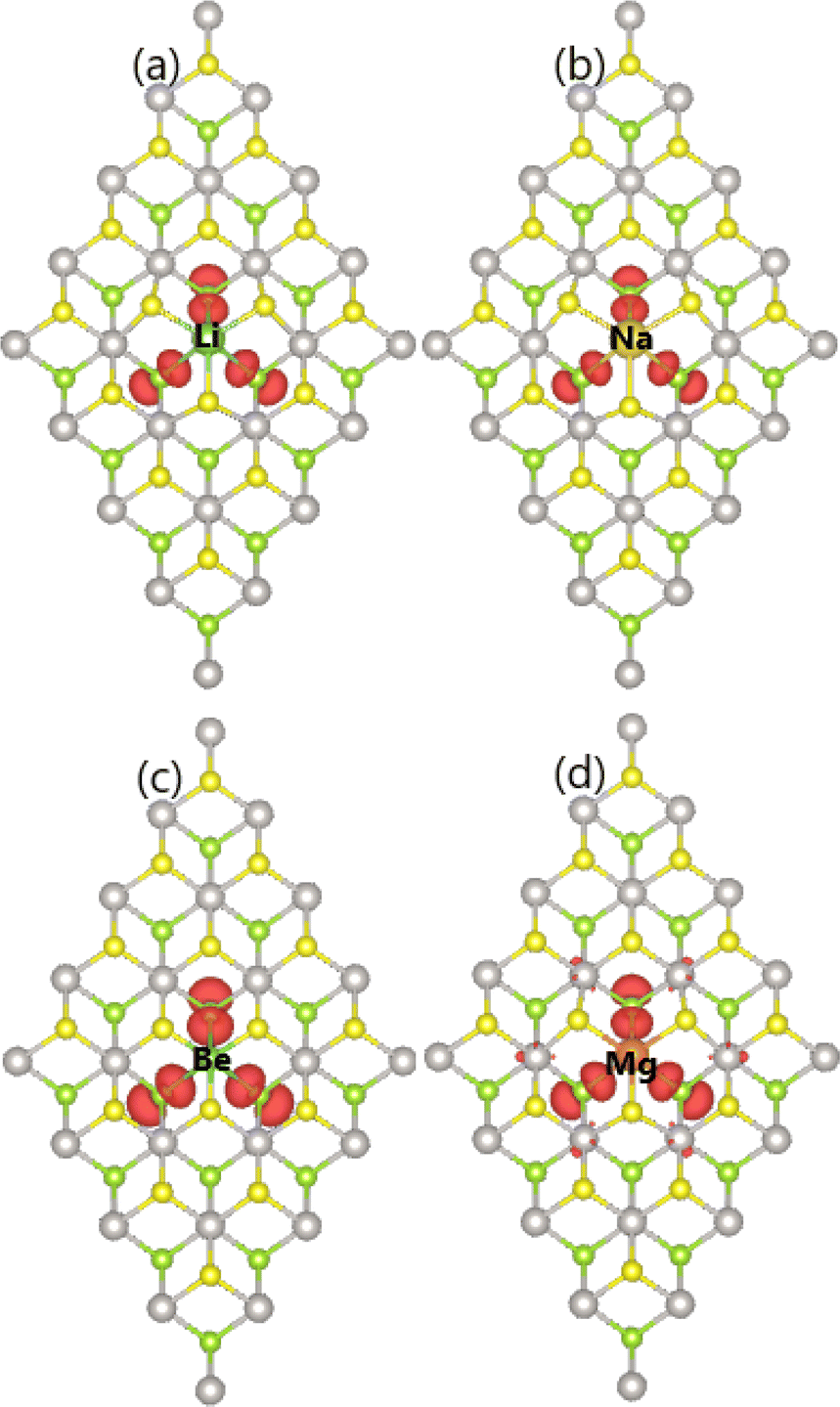 | ||
| Fig. 7 Spin density (iso-surface value: 0.005 e Å−3) in (a) LiPt, (b) NaPt, (c) BePt, and (d) MgPt system. | ||
Fig. 8 shows PDOS spectra of metal impurities and their neighboring S and Se atoms. Note that the contribution of Li, Na, Be, and Mg atoms is considerably smaller than that of S and Se atoms, where their s-px,y,z states are observed. Most importantly, the middle-gap are built mainly by px and pz states of S and Se atoms, which regulate the ground-state electronic behavior. The spin-polarized profiles suggest that Se-pz state originates mainly the magnetism in the doped PtSSe structures, where small contribution to magnetism may come also from S-px state. Weak electronic hybridization and charge transfer process may testify the ionic chemical bonds D-S and D-Se (D = Li, Na, Be, and Mg). This feature is confirmed by the electron localization function, which shows negligible electron function in the region between metal impurities and their neighboring S and Se atoms (see Fig. S5 of the ESI† file).
 | ||
| Fig. 8 Projected density of states of impurity and its neighboring S/Se atoms in (a) LiPt, (b) NaPt, (c) BePt, and (d) MgPt system. | ||
D. Effects of doping at S and Se sublattices
Now, doping with VA-group (P and As) atoms at S (PS and AsS) and Se (PSe and AsSe) sublattices is investigated. Firstly, doping energy Ed and cohesive energy Ec are calculated using eqn (3) and (4) modified for these cases as follow:| Ef = Em–Ch+D − Em + μCh − μD | (5) |
 | (6) |
The spin-polarized band structures displayed in Fig. 9 show new features different from that of pure monolayer, which are derived from new middle-gap flat energy branches around the Fermi level. Specifically, one new state below the spin-up Fermi level and the other above the spin-down Fermi level of PS, PSe, and AsS systems induce strong spin polarization at the vicinity of the Fermi level. Consequently, these systems can be classified as 2D diluted magnetic semiconductor materials with the spin-up/spin-down band gaps of 1.22/0.54, 1.29/0.55, and 1.22/0.23 eV, respectively. Dissimilarly, the spin-down state is metallized when doping PtSSe monolayer with As atom at Se site, such that the half-metallicity emerges in AsSe system. In this case, spin-up state exhibits the semiconductor character with a band gap of 1.39 eV. Further, the Bader charge analysis is carried out to analyze the interactions between P and As impurities with the host monolayer. Interestingly, P and As impurities act as charge losers transferring charge quantity of 0.33/0.36 and 0.44/0.37 e to the host monolayer when substituting S/Se atom, respectively. This feature is derived from the slightly less electronegative nature of P and As atoms in comparison with the surrounding Pt atoms.60 However, the calculated electron localization functional suggests that P–Pt and As–Pt chemical bonds are predominantly covalent (see Fig. S6 of the ESI† file), which is derived from the electronic hybridization as analyzed below.
 | ||
| Fig. 9 Spin-resolved band structure (the Fermi level is set to 0 eV; spin-up: black curves; spin-down: red curves) of (a) PS, (b) PSe, (c) AsS, and (d) AsSe system. | ||
The spin polarization in the band structures implies significant magnetization of PtSSe monolayer. It is found a total magnetic moment of 1.00 μB when doping with P atom at both S and Se sites, while AsS and AsSe systems have total magnetic moment of 0.99 μB. Therefore, doping with VA-group atoms can be introduced as an effective method to induce magnetism in PtSSe monolayer. Consequently, new half-metallic and diluted magnetic semiconductor systems are successfully developed for spintronic applications. Furthermore, the magnetization is also reflected in the spin density surface illustrated in Fig. 10. Note that P and As impurities produce mainly the magnetic properties of PS, PSe, and AsS systems. Meanwhile, the AsSe system magnetism is originated mainly from the second neighbor S atoms from doping site. Considering the thermodynamic favorability of P doping at Se site in comparison with other dopant atoms, the spin ordering in PSe system is further studied. It is found that the antiferromagnetic → non-magnetic → ferromagnetic transition takes place according to increase the distance between P impurity atoms (see Fig. S7 and S8 of the ESI† file for the spin density and spin-polarized band structure, respectively).
 | ||
| Fig. 10 Spin density (iso-surface value: 0.005 e Å−3) in (a) PS, (b) PSe, (c) AsS, and (d) AsSe system. | ||
PDOS spectra of VA-group impurities and their surrounding Pt atoms are given in Fig. 11. Note that the middle-gap states are derived mainly from P-pz and As-pz states with small contribution of Pt-dxz and Pt-dz2 states. These states exhibit strong spin polarization around the Fermi level. Therefore, one can conclude that the magnetism is originated mainly from pz state of VA-group impurities, where small contribution may come also from the unbalanced charge distribution between spin channels of Pt-d orbital. In the case of AsSe system, it can be noted also important contribution of As-px and As-py states around the Fermi level. To investigate with more details the origin of AsSe system magnetism, PDOS spectra of its magnetic S atoms are given in Fig. 12. From the figure, it can be attributed the appearance of magnetism to S-px and S-pz states.
 | ||
| Fig. 11 Projected density of states of impurity and its neighboring Pt atom in (a) PS, (b) PSe, (c) AsS, and (d) AsSe system. | ||
 | ||
| Fig. 12 Projected density of states of the magnetic S atoms in SeAs system. | ||
IV. Conclusions
In summary, the effects of vacancy and doping on the PtSSe monolayer electronic and magnetic properties have been systematically investigated using first-principles calculations. Pristine monolayer possesses good mechanical, dynamical, and thermal stability. This is a 2D semiconductor materials with a relative large band gap, whose chemical bonds are predominantly covalent generated by the strong electronic hybridization between Pt-5d, S-3p, and Se-4p orbitals. By creating vacancy and realizing doping process, new middle-gap states are developed in PtSSe monolayer to determine the ground-state electronic and magnetic properties. Our calculations assert that single S vacancy and Se vacancy causes considerable band gap reduction to make possible harvesting a wider light regime, which can be attributed to a larger charge distribution in 5d orbital of Pt atoms around the vacancy sites. Meanwhile, the monolayer is significantly magnetized by single Pt vacancy, doping with alkali metals (Li and Na atoms), doping with alkaline earth metals (Be and Mg atoms), and doping with VA-group atoms (P and As atoms). It has been found that VPt, LiPt, NaPt, and AsSe are 2D half-metallic systems, while the diluted magnetic semiconductor nature is induced in BePt, MgPt, PS, PSe, and AsS systems, respectively. In all cases, impurities and those atoms closest to the defect/doping sites produce mainly the system magnetic properties. In addition, Bader charge analysis indicates that the host monolayer attracts charge from impurities. Moreover, negative cohesive energies suggest good structural-chemical stability all the defect/doped systems. Our work may introduce new multifunctional 2D materials promising for optoelectronic and spintronic applications, which are made from a non-magnetic PtSSe monolayer.Data availability
Data related to this study are available upon reasonable request.Conflicts of interest
The authors declare that they have no known competing financial interests or personal relationships that could have appeared to influence the work reported in this paper.Acknowledgements
Calculations were performed in DGCTIC-UNAM Supercomputing Center (projects LANCAD-UNAM-DGTIC-368). D. M. Hoat expresses his gratitude to all the valuable support from Duy Tan University, who is going to celebrate its 30th anniversary of establishment (Nov. 11, 1994–Nov. 11, 2024) towards “Integral, Sustainable and Stable Development”.References
- K. S. Novoselov, A. K. Geim, S. V. Morozov, D.-e. Jiang, Y. Zhang, S. V. Dubonos, I. V. Grigorieva and A. A. Firsov, Science, 2004, 306, 666–669 CrossRef CAS PubMed.
- M. J. Allen, V. C. Tung and R. B. Kaner, Chem. Rev., 2010, 110, 132–145 CrossRef CAS PubMed.
- A. K. Geim and K. S. Novoselov, Nat. Mater., 2007, 6, 183–191 CrossRef CAS PubMed.
- T. Radsar, H. Khalesi and V. Ghods, Opt. Quantum Electron., 2021, 53, 1–38 CrossRef.
- J. E. Johns and M. C. Hersam, Acc. Chem. Res., 2013, 46, 77–86 CrossRef CAS PubMed.
- H. Zhang, E. Bekyarova, J.-W. Huang, Z. Zhao, W. Bao, F. Wang, R. C. Haddon and C. N. Lau, Nano Lett., 2011, 11, 4047–4051 CrossRef CAS PubMed.
- Y.-W. Son, M. L. Cohen and S. G. Louie, Phys. Rev. Lett., 2006, 97, 216803 CrossRef PubMed.
- M. Y. Han, B. Özyilmaz, Y. Zhang and P. Kim, Phys. Rev. Lett., 2007, 98, 206805 CrossRef PubMed.
- L. Yuan, J. Ge, X. Peng, Q. Zhang, Z. Wu, Y. Jian, X. Xiong, H. Yin and J. Han, AIP Adv., 2016, 6, 125201 CrossRef.
- F. Liu, Prog. Surf. Sci., 2021, 96, 100626 CrossRef CAS.
- L. Tang, J. Tan, H. Nong, B. Liu and H.-M. Cheng, Acc. Mater. Res., 2020, 2, 36–47 CrossRef.
- L. Jiao, H. J. Liu, J. Chen, Y. Yi, W. Chen, Y. Cai, J. Wang, X. Dai, N. Wang and W. K. Ho, et al., New J. Phys., 2015, 17, 053023 CrossRef.
- D. Deng, K. Novoselov, Q. Fu, N. Zheng, Z. Tian and X. Bao, Nat. Nanotechnol., 2016, 11, 218–230 CrossRef CAS PubMed.
- J. Su, G.-D. Li, X.-H. Li and J.-S. Chen, Adv. Sci., 2019, 6, 1801702 CrossRef PubMed.
- J. Cheng, C. Wang, X. Zou and L. Liao, Adv. Opt. Mater., 2019, 7, 1800441 CrossRef.
- J. Shim, H.-Y. Park, D.-H. Kang, J.-O. Kim, S.-H. Jo, Y. Park and J.-H. Park, Adv. Electron. Mater., 2017, 3, 1600364 CrossRef.
- Y. Fang, Y. Ge, C. Wang and H. Zhang, Laser Photonics Rev., 2020, 14, 1900098 CrossRef CAS.
- J. Wu, H. Ma, P. Yin, Y. Ge, Y. Zhang, L. Li, H. Zhang and H. Lin, Small Sci., 2021, 1, 2000053 CrossRef CAS.
- H. Tao, Q. Fan, T. Ma, S. Liu, H. Gysling, J. Texter, F. Guo and Z. Sun, Prog. Mater. Sci., 2020, 111, 100637 CrossRef CAS.
- Y. Xue, Q. Zhang, W. Wang, H. Cao, Q. Yang and L. Fu, Adv. Energy Mater., 2017, 7, 1602684 CrossRef.
- N. Rohaizad, C. C. Mayorga-Martinez, M. Fojtu, N. M. Latiff and M. Pumera, Chem. Soc. Rev., 2021, 50, 619–657 RSC.
- D. Chauhan, M. Ashfaq, N. Talreja and R. V. Managalraja, J. Biomed. Res. Environ. Sci., 2021, 2766, 2276 Search PubMed.
- E. C. Ahn, npj 2D Mater. Appl., 2020, 4, 17 CrossRef CAS.
- W. Han, APL Mater., 2016, 4, 032401 CrossRef.
- W. Choi, N. Choudhary, G. H. Han, J. Park, D. Akinwande and Y. H. Lee, Mater. Today, 2017, 20, 116–130 CrossRef CAS.
- L. Debbichi, O. Eriksson and S. Lebegue, Phys. Rev. B: Condens. Matter Mater. Phys., 2014, 89, 205311 CrossRef.
- H. Wang, H. Feng and J. Li, Small, 2014, 10, 2165–2181 CrossRef CAS PubMed.
- J. Xi, T. Zhao, D. Wang and Z. Shuai, J. Phys. Chem. Lett., 2014, 5, 285–291 CrossRef CAS PubMed.
- K. F. Mak and J. Shan, Nat. Photonics, 2016, 10, 216–226 CrossRef CAS.
- L. Cao, MRS Bull., 2015, 40, 592–599 CrossRef CAS.
- W. Huang, H. Da and G. Liang, J. Appl. Phys., 2013, 113, 104304 CrossRef.
- G. Zhang and Y.-W. Zhang, J. Mater. Chem. C, 2017, 5, 7684–7698 RSC.
- G. H. Shin, C. Park, K. J. Lee, H. J. Jin and S.-Y. Choi, Nano Lett., 2020, 20, 5741–5748 CrossRef CAS PubMed.
- A. Sharma, R. Mahlouji, L. Wu, M. A. Verheijen, V. Vandalon, S. Balasubramanyam, J. P. Hofmann, W. E. Kessels and A. A. Bol, Nanotechnology, 2020, 31, 255603 CrossRef CAS PubMed.
- N. Peimyoo, J. Shang, C. Cong, X. Shen, X. Wu, E. K. Yeow and T. Yu, ACS Nano, 2013, 7, 10985–10994 CrossRef CAS PubMed.
- N. Peimyoo, W. Yang, J. Shang, X. Shen, Y. Wang and T. Yu, ACS Nano, 2014, 8, 11320–11329 CrossRef CAS PubMed.
- A.-Y. Lu, H. Zhu, J. Xiao, C.-P. Chuu, Y. Han, M.-H. Chiu, C.-C. Cheng, C.-W. Yang, K.-H. Wei and Y. Yang, et al., Nat. Nanotechnol., 2017, 12, 744–749 CrossRef CAS PubMed.
- J. Zhang, S. Jia, I. Kholmanov, L. Dong, D. Er, W. Chen, H. Guo, Z. Jin, V. B. Shenoy and L. Shi, et al., ACS Nano, 2017, 11, 8192–8198 CrossRef CAS PubMed.
- Y. Wang, L. Li, W. Yao, S. Song, J. Sun, J. Pan, X. Ren, C. Li, E. Okunishi and Y.-Q. Wang, et al., Nano Lett., 2015, 15, 4013–4018 CrossRef CAS PubMed.
- Y. Zhao, J. Qiao, P. Yu, Z. Hu, Z. Lin, S. P. Lau, Z. Liu, W. Ji and Y. Chai, Adv. Mater., 2016, 28, 2399–2407 CrossRef CAS PubMed.
- W.-L. Tao, J.-Q. Lan, C.-E. Hu, Y. Cheng, J. Zhu and H.-Y. Geng, J. Appl. Phys., 2020, 127, year CrossRef.
- R. Peng, Y. Ma, B. Huang and Y. Dai, J. Mater. Chem. A, 2019, 7, 603–610 RSC.
- Q. Wu, L. Cao, Y. S. Ang and L. K. Ang, Nano Express, 2020, 1, 010042 CrossRef.
- H. Cui, Q. Zhang, H. Liu and X. Peng, Vacuum, 2022, 198, 110887 CrossRef CAS.
- G.-D. Zhao, X. Liu, T. Hu, F. Jia, Y. Cui, W. Wu, M.-H. Whangbo and W. Ren, Phys. Rev. B, 2021, 103, 014438 CrossRef CAS.
- M. Kan, J. Zhou, Q. Sun, Y. Kawazoe and P. Jena, J. Phys. Chem. Lett., 2013, 4, 3382–3386 CrossRef CAS PubMed.
- W. Kohn and L. J. Sham, Phys. Rev., 1965, 140, A1133 CrossRef.
- G. Kresse and J. Furthmüller, Comput. Mater. Sci., 1996, 6, 15–50 CrossRef CAS.
- G. Kresse and J. Furthmüller, Phys. Rev. B: Condens. Matter Mater. Phys., 1996, 54, 11169 CrossRef CAS PubMed.
- J. P. Perdew, K. Burke and M. Ernzerhof, Phys. Rev. Lett., 1996, 77, 3865 CrossRef CAS PubMed.
- A. V. Krukau, O. A. Vydrov, A. F. Izmaylov and G. E. Scuseria, J. Chem. Phys., 2006, 125, 224106 CrossRef PubMed.
- H. J. Monkhorst and J. D. Pack, Phys. Rev. B: Solid State, 1976, 13, 5188 CrossRef.
- G. Henkelman, A. Arnaldsson and H. Jónsson, Comput. Mater. Sci., 2006, 36, 354–360 CrossRef.
- M. Yu and D. R. Trinkle, J. Chem. Phys., 2011, 134, year CrossRef PubMed.
- F. Mouhat and F.-X. Coudert, Phys. Rev. B: Condens. Matter Mater. Phys., 2014, 90, 224104 CrossRef.
- A. Togo, J. Phys. Soc. Jpn., 2023, 92, 012001 CrossRef.
- P. A. L. Sino, L.-Y. Feng, R. A. B. Villaos, H. N. Cruzado, Z.-Q. Huang, C.-H. Hsu and F.-C. Chuang, Nanoscale Adv., 2021, 3, 6608–6616 RSC.
- X. Li and J. Yang, Natl. Sci. Rev., 2016, 3, 365–381 CrossRef CAS.
- X. Li and X. Wu, Wiley Interdiscip. Rev.: Comput. Mol. Sci., 2016, 6, 441–455 CAS.
- A. L. Allred, J. Inorg. Nucl. Chem., 1961, 17, 215–221 CrossRef CAS.
Footnote |
| † Electronic supplementary information (ESI) available. See DOI: https://doi.org/10.1039/d4ra02071e |
| This journal is © The Royal Society of Chemistry 2024 |