
 Open Access Article
 This Open Access Article is licensed under a Creative Commons Attribution-Non Commercial 3.0 Unported Licence
Mechanisms of manipulating valley splitting in MoTe2/MnS2 van der Waals heterostructure by electric field and strains†
Xiao Liang *ab,
Yiqun Liua,
Tianjun Zhonga,
Ting Yanga,
Jie Lia,
Li Luoa,
Gao Dongb,
Yanhong Chena,
Xuelian Luoa,
Tingting Tang*a and
Lei Bi*b
*ab,
Yiqun Liua,
Tianjun Zhonga,
Ting Yanga,
Jie Lia,
Li Luoa,
Gao Dongb,
Yanhong Chena,
Xuelian Luoa,
Tingting Tang*a and
Lei Bi*b
aOptoelectronic Sensor Devices and Systems Key Laboratory of Sichuan Provincial University, Chengdu University of Information Technology, Chengdu 610225, China. E-mail: liangxiao@cuit.edu.cn; skottt@163.com
bNational Engineering Research Center of Electromagnetic Radiation Control Materials, University of Electronic Science and Technology of China, Chengdu 610054, China. E-mail: bilei@uestc.edu.cn
First published on 27th March 2024
Abstract
In this study, we discuss the tunability of valley splitting using first-principles calculations with a monolayer MoTe2 and layered ferromagnetic MnS2 heterostructure as an example. We observe that, due to the magnetic proximity effect (MPE) at the interface, a monolayer of MoTe2 can exhibit a significant valley splitting of 55.2 meV. The production of the interlayer dipoles with spin-adapted configuration could be the origin of MPE at the interface. Furthermore, the valley splitting can be regulated continuously by the perpendicular electric field and biaxial strain. Interestingly, the valley splitting increases with the increasing induced magnetic moments in MoTe2 by applying an electric field while the inverse laws are presented by applying biaxial strains, which indicates that the mechanisms of valley splitting manipulating in these two ways are quite different. The calculation results suggest that the electric field influences the electric dipole distributions at the interface, which determines the induced magnetic moments in monolayer MoTe2, and results in valley splitting variations. However, biaxial strains not only affect MPE at the interface but also the intrinsic spin splitting caused by spin–orbital coupling (SOC) effects of monolayer MoTe2 itself and the latter is even the dominating mechanism of valley splitting variations.
1. Introduction
Recent studies of two-dimensional transition-metal dichalcogenides (2D-TMDCs) have revealed many new phenomena such as the quantum spin/valley anomalous Hall effect,1–3 valley-dependent optoelectronics,4 spin/valley polarization of plasmons,5–7 magneto-optical conductivity,8 electrical transport of valley carriers,9–11 and spin-polarized edge currents,12 which have generated intense interest in these valley-polarized systems. As a result of strong intrinsic spin–orbit coupling (SOC) and inversion symmetry broken effect, 2D-TMDCs exhibit distinct valley-selective states with different angular momenta, named K and K′ valleys, which brings a new degree of freedom to photoelectric devices.13–15 Therefore, 2D-TMDCs have emerged as promising candidates for optical, nanoelectronics and optoelectronics applications, propelling the development of valleytronics.16–20 Despite significant advances in 2D-TMDC based valleytronics devices, maneuvering a pair of valleys in 2D-TMDCs still poses a significant challenge because the pair is locked by the time-reversed symmetry (TRS) energy degradation, limiting the device's tunability of the valleys.21,22To solve this problem, it is necessary to break TRS in 2D-TMDCs, and then dynamically and efficiently polarize the K and K′ valleys, which requires exciting carriers to produce a transient non-equilibrium distribution in both valleys. One effective strategy to break this correlation and induce non-equilibrium carrier distributions in the valleys is through the utilization of ultrafast circularly polarized laser pumping, which leverages the optical Stark effect.13,23–25 Nevertheless, optical pumping is also facing the challenge of precise control and is constrained by the inherently short carrier lifetimes. An alternative strategy involves applying a vertical magnetic field, leveraging the Zeeman effect to break the valley degeneracy.14,22 However, achieving significant valley splitting typically demands the use of strong magnetic fields exceeding 10 tesla, which greatly enhances the power dissipation and is inconvenient to miniaturization and integration of nano-devices.
Recent research studies have proposed an approach to introduce non-range magnetic orders to 2D-TMDCs through magnetic proximity effects (MPE),15,26 resulting from their adjacency to ferromagnetic materials such as EuO,26 EuS,27–29 MnO,21 Fe2O3,30 and YMnO3.31 However, it is worth noting that the application of the bulk substrates inherently constrains the scalability of devices in the nanoscale regime. Traditional magnetic materials, due to the principle of lattice adaptation, are difficult to prepare in situ heterojunctions. In addition to the aforementioned methods, a promising avenue for enhanced valley control involves the creation of vertical two-dimensional magnetic van der Waals (vdW) heterostructures employing layered two-dimensional materials. This particular approach offers the advantage of forming exceptionally clean interfaces, thereby mitigating impurity scattering effects. Furthermore, it minimizes the impact of lattice mismatch, a factor that can otherwise weaken the observed valley splitting.15 The inherent flexibility of layer stacking processes offers a versatile means of creating van der Waals heterostructures by seamlessly combining integration of the layered ferromagnets with a variety of 2D materials, including graphene, Weyl semimetals such as WTe2, and superconductors such as NbSe2.32 The bond-free vdW interactions in heterostructure provide a natural interfacial strain relaxation,33 and vdW heterostructure may exhibit superior properties through strain.34 Furthermore, the advantage of constructing heterostructures exclusively from 2D materials cannot be overstated, as it streamlines the integration process when fabricating valley electronic devices. Notably, recent theoretical predictions and experimental discoveries concerning 2D WSe2/CrI3 heterostructures have unveiled their remarkable attributes, demonstrating significant valley splitting and the potential for optically controllable valley pseudo-spin.35 In view of these advantages, the strategic engineering and the assembly of 2D layered magnetic/semiconductor heterostructures assume paramount importance in the exploration of spin valley splitting phenomena. A recent development of great significance lies in the theoretical prediction of MnS2 monolayers as ferromagnetic semiconductor materials exhibiting a high Curie temperature.36,37 What makes this particularly compelling is the minimal lattice mismatch observed between MoTe2 and MnS2 monolayers, measuring a mere 3.52 Å for MoTe2 (ref. 38–40) and 3.47 Å for MnS2.36 This observation underpins the promise of the MoTe2/MnS2 heterostructure, which has the potential to manifest valleytronics properties and holds great promise for a wide array of applications in valleytronics devices.
We employed density functional theory in this study to study the precise modulation of valley degrees of freedom within monolayer MoTe2/MnS2 heterostructures. The TRS of the MoTe2 monolayer undergoes perturbation due to the MPE arising from the ferromagnetic (FM) MnS2 substrate. This interaction leads to a large degree of substantial static valley polarization within the heterostructure, accompanied by a discernible valley splitting of 55 meV. We meticulously explored the manipulation of both spin and valley properties by subjecting the system to an electric field oriented in the vertical direction and biaxial strain. Notably, our analysis reveals that in the K-valley and K′-valley, the Berry curvatures exhibit opposing signs. These findings underscore the exciting potential for the application of 2D magnetic vdW heterostructures in the realm of valley electronic devices.
2. Computational method
In this work, all first-principles calculations based on density functional theory (DFT) were performed using the Vienna Ab into Simulation Package (VASP).41 The electron–ion interaction is solved by the method of the projected enhanced wave. To characterize the electron exchange–correlation interaction, the generalized gradient approximation (GGA) in the Perdew–Burke–Ernzerhof (PBE) functional was employed.42 The cut-off energy was set to 500 eV, and a vacuum layer of 20 Å along the z-direction was introduced to mitigate the effect of periodic boundary conditions. In order to correctly describe the strongly correlated electrons in the partially filled d subshells, the GGA + Ueff method was employed, with Ueff set to 3.9 eV for Mn,36,43,44 which previous reports have conducted tests on,45,46 and the results are in excellent accordance with the experimental data.47 Various values of Ueff were also explored in our study to demonstrate the appropriateness of the chosen Ueff and the general results of our study were not affected by the qualitative tests.48 For MoTe2, MnS2, and MoTe2/MnS2 heterostructures, the Brillouin zone integration was sampled using a 12 × 12 × 1 gamma-pack k-point meshes for both structure optimization and static electronic structure calculations, and adjusting the direction of the magnetic moment by adjusting the SAXIS parameter in INCAR for band structure calculations. For the calculation of the Berry curvature, the maximally localized Wannier functions (MLWFs)49 from WANNIER90 (ref. 50) were used. The force convergence criterion was set to be less than 0.01 eV Å−1, and the electron iteration convergence criterion was established at 1 × 10⁻⁵ eV, ensuring complete relaxation of the structural parameters and atomic positions. Additionally, the SOC effect was taken into account in electronic structure calculations.3. Results and discussion
The optimized structures of the MnS2 with the space group P3m1, MoTe2 with the space group P6/mmc and MoTe2/MnS2 heterostructures are illustrated in Fig. 1a–c. The lattice constants for the optimized monolayers of MnS2 and MoTe2 were determined to be 3.47 Å and 3.52 Å, respectively. These values are in agreement with those from the earlier research. Under the aforementioned lattice parameters, the monolayers of MnS2 and MoTe2 exhibit vertical stacking of their primitive cells, resulting in a lattice mismatch of approximately 1.44%, laying the groundwork for constructing the MoTe2/MnS2 vdWHs comprising MoTe2 and MnS2. In Fig. 1c, ‘d’ represents the layer spacing at the energy nadir of the heterostructure formation between MoTe2 and MnS2. MoTe2 and MnS2 monolayers exhibit four distinct configurations arising from the translational and rotational operations, as shown in Fig. 1d, AA: Te1 and Te2 atoms are above the S1 atoms and the Mo atom is above the Mn atom, AA*: Te1 and Te2 atoms are above the S2 atoms and the Mo atom is above the Mn atom, AB: Te1 and Te2 atoms are above the S2 atoms and the Mo atom is above the S1 atom, AB*: Te1 and Te2 atoms are above the S2 atoms and the Mo atom is above the S1 atom.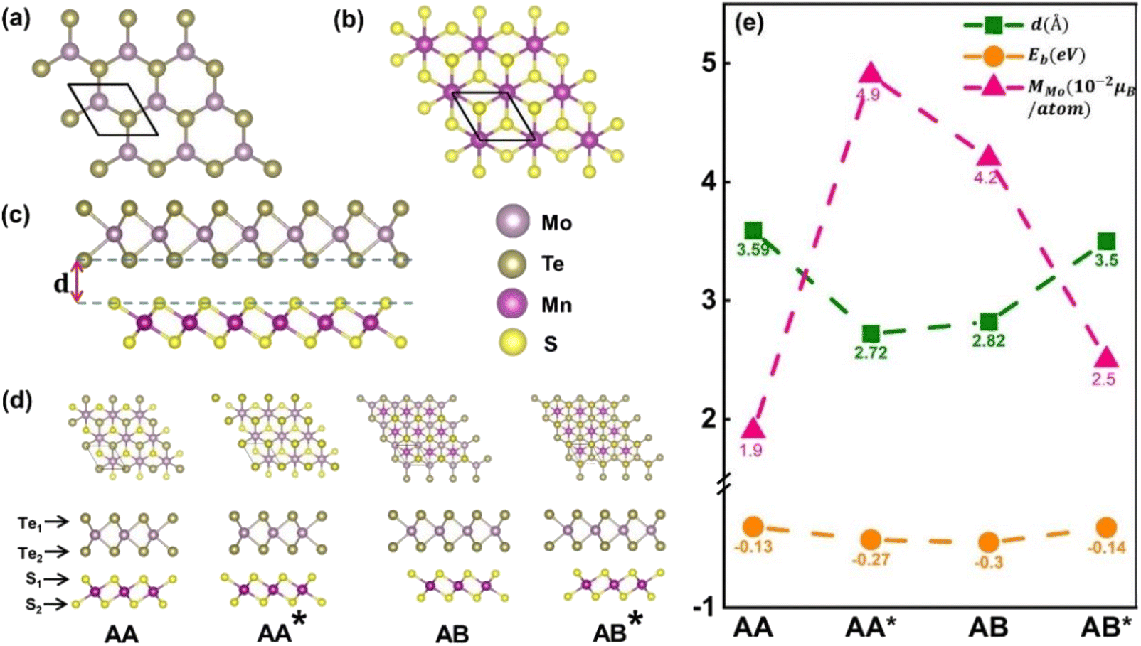 | ||
| Fig. 1 The optimized structures of (a) MnS2 and (b) MoTe2 monolayers, (c) side view of the MnS2/MoTe2 vdWHs, (d) top and side views of four stacked conformations. (e) Layer spacing of the four conformations, d, binding energy Eb and magnetic moments of Mo atoms. | ||
To ascertain the most stable configuration, the binding energy Eb for the MoTe2/MnS2 heterostructures can be computed using the following relationship
| Eb = EMoTe2/MnS2 − EMoTe2 − EMnS2 |
Fig. 2a and b illustrate the band structures at the K-valley and K′-valley, respectively. The solid red and blue lines represent the band edges of spin-up and spin-down states in the MoTe2 band structure. Δc/vsoc represents the spin splitting of MoTe2 without an applied magnetic field, which arises from the spin–orbit coupling in MoTe2 itself. ΔC/V,+/−spin represents the spin splitting of MoTe2 under a magnetic field, where ‘C’ and ‘V’ denote the conduction band (CB) and valence band (VB), and ‘+’ and ‘−’ denote the K-valley and K′-valley, respectively. ΔCB/VB in the figure represents the valley splitting in the conduction band/valence band. We define ΔCB/VB = ECB1/VB1′ − ECB1′/VB1.  , Δ+opt and Δ−opt represent the absorption energy levels for left- and right-polarized light at the K-valley and K′-valley, respectively. We define the total K and K′ valley Zeeman splitting as EZ = Δ+opt − Δ−opt.
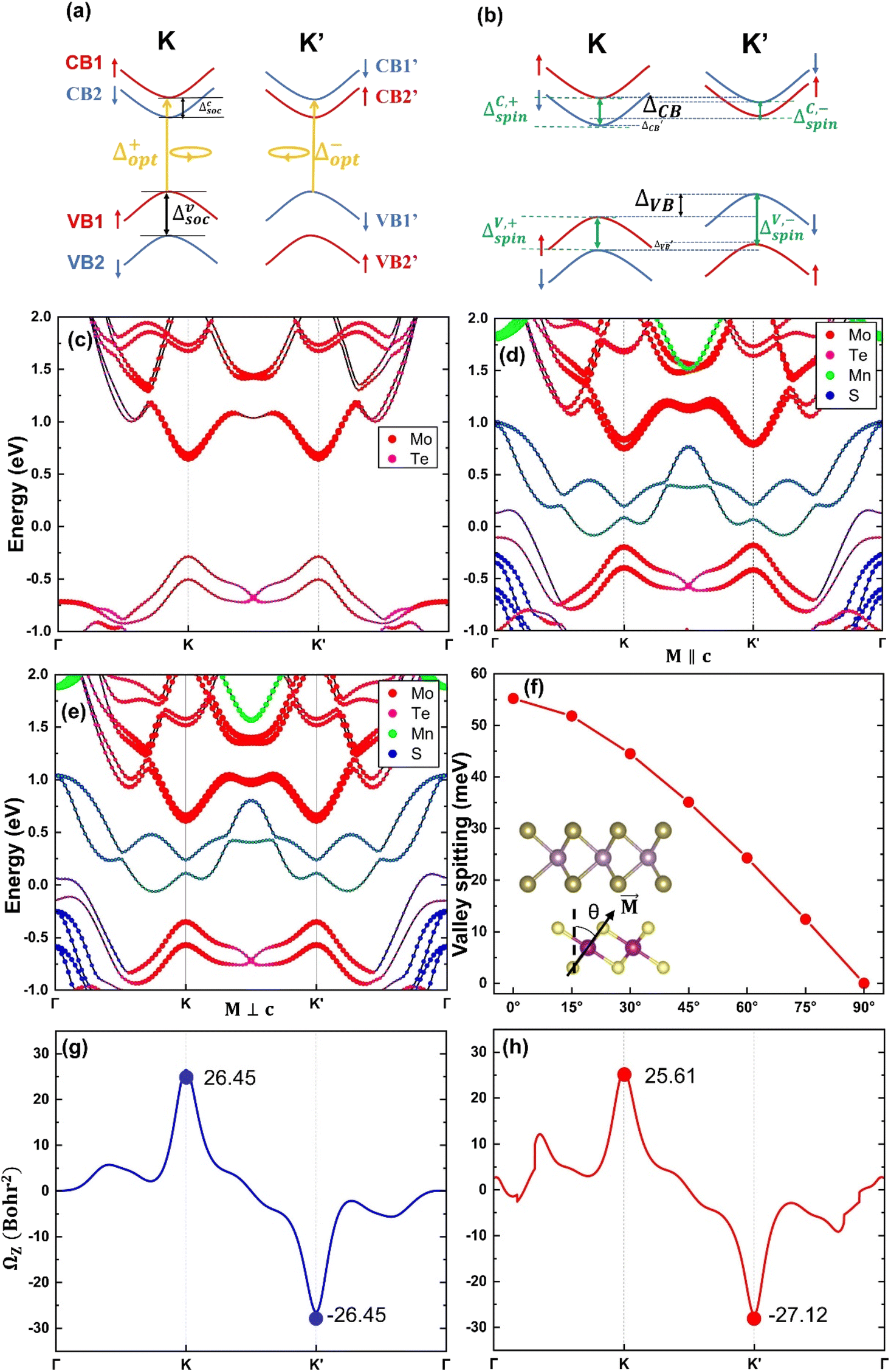 | ||
| Fig. 2 (a) Schematic band structure of the K-valley and K′-valley without an applied magnetic field. Δ+opt, and Δ−opt represent the absorption energy levels for left- and right-polarized light in the K-valley and K′-valley, respectively. Ecsoc and Evsoc represent the spin splitting in the conduction band and valence band induced by SOC, respectively. The valley spin states of spin up and spin down are indicated by red up arrows and blue down arrows, respectively. (b) Schematic band structure of the KK′ valleys under applied magnetic field. ΔCB and ΔVB represent the energy valley splitting of the conduction band and valence band, respectively. ΔC,+spin, ΔC,−spin denote the spin splitting of the conduction band at the K and K′ points, respectively, and ΔV,+spin, ΔV,−spin represent the spin splitting of the valence band in the K-valley and K′-valley, respectively. (c) Band structure of the monolayer MoTe2. (d) Band structure of the MoTe2/MnS2 heterostructure with the direction of magnetization parallel to the z-axis. (e) Band structure of the MoTe2/MnS2 heterostructure with the direction of magnetization perpendicular to the z-axis. (f) Variation of the valley splitting with different magnetization angles. The illustration shows the angle of magnetization. (g) Berry curvature of monolayer MoTe2. (h) Berry curvature of the MoTe2/MnS2 heterostructure. | ||
The atom-projected band structures of MoTe2 and MoTe2/MnS2 heterostructures are depicted in Fig. 2c and d, respectively. Notably, we observed that the K-valley and K′-valley of MoTe2 are strongly retained within the heterostructures. In the isolated MoTe2 structure, the electronic band structure exhibits varying degrees of spin splitting at the conduction band (CB) and valence band (VB) edges, primarily due to the influence of SOC. However, owing to the constraints imposed by TRS, the spin splitting in the K-valley and K′-valley remains symmetric, thereby precluding the occurrence of the valley Zeeman splitting. Upon forming a heterostructure with MnS2, the MPE induces a limited magnetic moment in MoTe2, thereby breaking the TRS inherent in the band structure. Consequently, the spin splitting in the K-valley and K′-valley ceases to be symmetric, giving rise to the emergence of valley Zeeman splitting. Remarkably, the valley Zeeman splitting magnitude in MoTe2 is 55.2 meV, which is greater than the reported values of valley splitting in MoTe2/CrI3 (5.9 meV),51 MoTe2/NiCl2 (32.5 meV),45 and MoTe2/EuO.26 Our computational findings bear substantial significance for prospective research endeavors. As exemplified in Fig. 2e, we scrutinized the atom-projected band structure of the MoTe2/MnS2 heterostructure under in-plane magnetization. In this configuration, MoTe2 undergoes magnetization without exhibiting valley Zeeman splitting, suggesting that only the out-of-plane magnetization exerts an influence on valley splitting. The nuanced relationship between magnetization direction and valley splitting is further elucidated in Fig. 2f, accompanied by an inset illustrating the magnetization angle. During the rotation of the Mn atom's direction of magnetization from the +Z direction (M∥c) to the in-plane direction (M⊥c), the valley splitting value remains positive, indicating that the valley splitting at the K-valley is higher than that at the K′-valley. Simultaneously, the value of valley Zeeman splitting gradually decreases from the maximum of 55.2 meV to 0. Therefore, the valley splitting can be adjusted by turning the direction of magnetization. Table 1 compares the spin splitting and valley splitting information for four different configurations. In the AA configuration, the valley Zeeman splitting is −11.9 meV, indicating that the valley splitting at the K′ point is more than the valley splitting at the K point. The AA* configuration exhibits the highest valley splitting, which may be attributed to the closest interlayer distance between MoTe2 and MnS2, resulting in a significant magnetic proximity effect and the largest magnetic moment for Mo, leading to the large valley splitting.
| ΔCB (meV) | ΔVB (meV) | ΔC,+spin (meV) | ΔC,−spin (meV) | ΔV,+spin (meV) | ΔV,−spin (meV) | EZ (meV) | |
|---|---|---|---|---|---|---|---|
| a ΔCB/VB representing the valley splitting in the conduction band/valence band. ΔC/V,+/−spin representing the spin splitting. EZ represents valley Zeeman splitting. | |||||||
| AA | −12.0 | 0.1 | 23.5 | 47.2 | 221.5 | 212.6 | −11.9 |
| AA* | −44 | 152.2 | 0.4 | 72.2 | 77.3 | 31.0 | 115.8 |
| AB | 37.3 | 17.8 | 84.2 | 10.5 | 200.2 | 238.0 | 55.2 |
| AB* | 19.8 | 14.4 | 54.8 | 15.8 | 204.7 | 236.1 | 34.2 |
To gain a better understanding of the large valley splitting induced by MPE, we build a low-energy effective Hamiltonian quantity according to the k·p model.15 The Hamiltonian quantity is denoted as:5,22
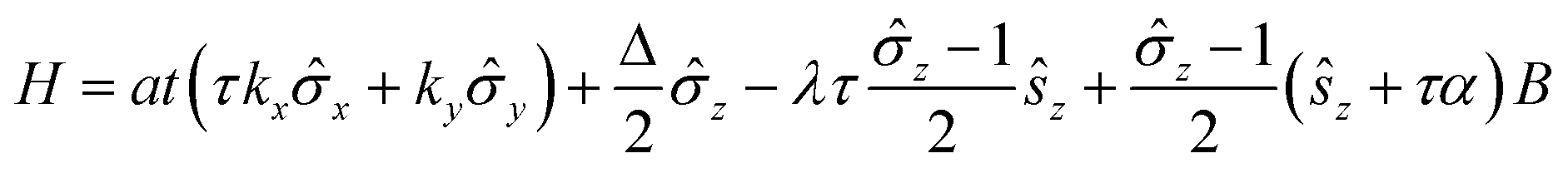
![[small sigma, Greek, circumflex]](https://www.rsc.org/images/entities/i_char_e111.gif) are the Pauli matrices for the two base functions: |dz2〉 and
are the Pauli matrices for the two base functions: |dz2〉 and 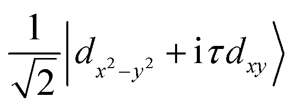 . In this context, τ = ±1 represents the valley index, and ŝz = ±1 represents the spin index. The Hamiltonian under consideration comprises four terms. The first three terms delineate the low-energy band dispersive characteristics of primitive monolayer MoTe2, while the fourth term encapsulates the exchange energy arising from the magnetic proximity effect. The valley splitting of the valence band denoted as ΔVB, can be deduced as
 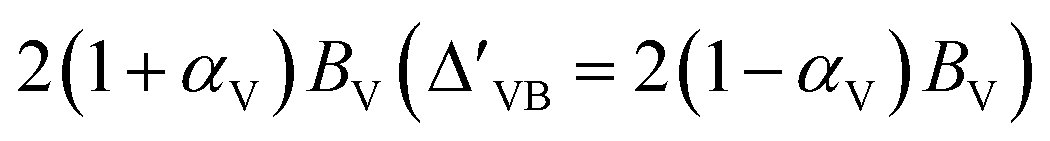 ), and the valley splitting of the conduction band, denoted as ΔCB, can be deduced as
  by substituting the valley index τ and spin index ŝz into the energy eigenvalue equation based on the Hamiltonian equation. By matching the intrinsic valley splitting to the first-principles calculations, ΔVB = 17.8 meV and ΔCB = 37.3 meV, the effective Zeeman field in the valence band, BV, is obtained as 9.1 meV, and the effective Zeeman field in the conduction band, BC, is obtained as 18.45 meV. In light of this, the valley Zeeman splitting arises from the interaction of the conduction and valence bands. Consequently, we define the entire equivalent Zeeman field, B, is given by B = BV + BC, which corresponds to 27.55 meV. Switching a Bohr magneton to 5.78 × 10⁻⁵ eV T−1, the effective Zeeman fields, BV and BC, correspond to a perpendicular magnetic field of 476 T to the monolayer MoTe2.
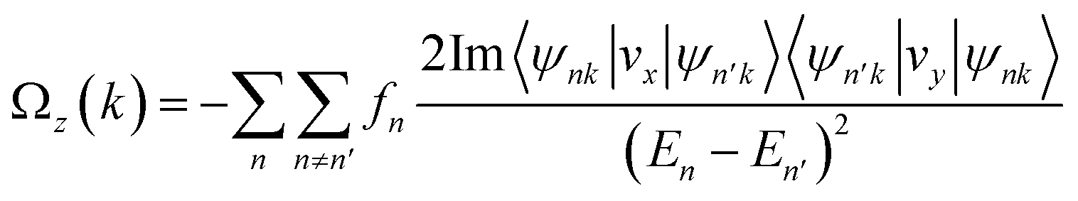
Because of the intrinsic inversion symmetry breaking of MoTe2, along the out-of-plane, carriers at the K-valley and K′-valley obtained a nonzero Berry curvature. According to the derivation of the Kubo formula, the Berry curvature can be represented as the sum of contributions from the occupation states53,54
The control of the degree of valley polarization is crucial for fulfilling various device design requirements, given the significant valley properties of the MoTe2/MnS2 heterostructure. By applying electric fields and in-plane biaxial strains to the MoTe2/MnS2 heterostructure, there is a desire to achieve modulation of the degree of valley splitting. Applying an external electric field is an easily achievable method in the laboratory to control the electronic structure or valley properties.55 We have calculated the band structure of MoTe2/MnS2 under an externally applied electric field in the z-direction. A positive electric field represents the field pointing from MnS2 towards MoTe2, while a negative electric field represents the electric field directed from MoTe2 to MnS2. Fig. 3a shows the change in spin splitting of the valence and conduction bands. When a negative electric field is applied, with increasing electric field strength, we can observe an increase and gradual enlargement of ΔC,+spin, ΔC,−spin, and ΔV,−spin compared to the case without an electric field, while ΔV,+spin gradually decreases. On the other hand, when a positive electric field is imposed, with the increasing electric field strength, we can observe a decrease and gradual reduction of ΔC,+spin, ΔC,−spin, and ΔV,−spin compared to the case without an electric field, while ΔV,+spin gradually increases. Fig. 3b presents the relationship between valley splitting EZ and the Mo atomic magnetic moment as a function of the applied electric field. When the negative electric field is imposed, the magnetic moment of Mo atoms and the magnitude of valley splitting EZ both increase with the increasing electric field. At an intensity of −0.3 V Å−1, the valley splitting reaches 56.6 meV. Conversely, when a positive electric field is applied, the magnetic moment of Mo atoms and the magnitude of valley splitting EZ are decreasing, with the valley splitting decreasing to 49.2 meV at an intensity of +0.3 V Å−1. These findings establish a positive correlation between the magnitude of valley splitting and the magnetic moment of Mo atoms. In Fig. 3c, we present a study of the influence of the electric field on the Berry curvature. Ωz(K) and Ωz(K′) represent the Berry curvature at the K-valley and K′-valley, respectively, while ΔΩ represents the difference in Berry curvature between these two points. The electric field has little impact on Ωz(K), but as the electric field increases, the value of Ωz(K′) decreases, leading to a decrease in the difference in Berry curvature ΔΩ. This trend suggests a potential connection between the behavior of Berry curvature and the magnetic moment of Mo atoms.
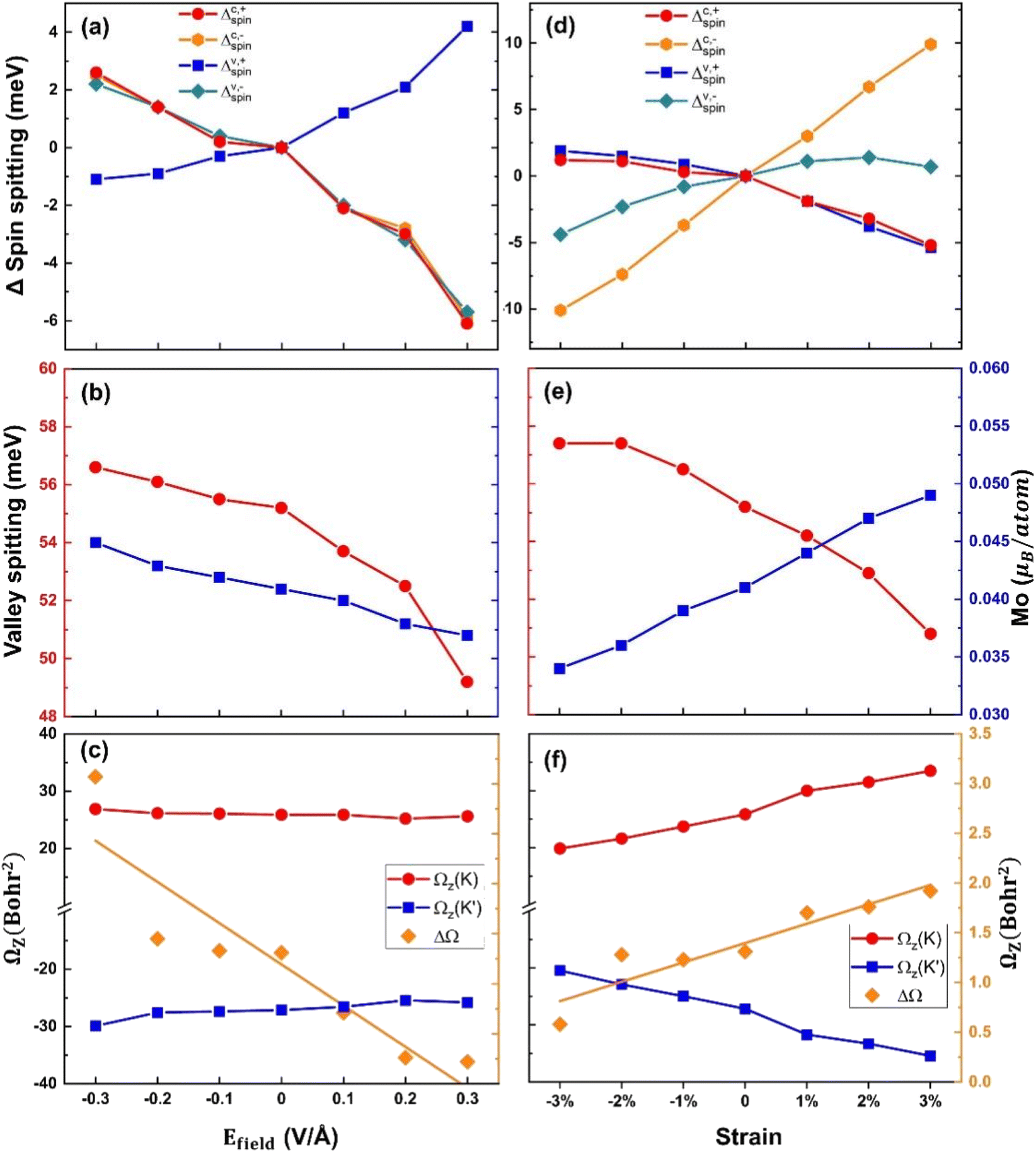 | ||
| Fig. 3 (a and d) Spin splitting in the conduction and valence bands at the K and K′ points. (b and e) Valley splitting in MoTe2/MnS2 and the induced magnetic moment of Mo; the red and blue curves represent the valley splitting and magnetic moment, respectively. (c and f) Berry curvature and the difference in Berry curvature at the K and K′ points. | ||
In-plane strain is also a useful method for controlling the electronic characteristics of heterostructures and can be performed through substrate tensile or bending.56–58 Biaxial strain can be defined using the following equation: ε = (a − a0)/a0, which refers to the relative difference in the lattice constants before and after applying biaxial strain. a0 is the lattice constant without the applied strain. a is the lattice constant after applying strain. Fig. 3d shows the variation in spin splitting under biaxial stress. We define tensile strain as a positive value and compressive strain as a negative value. With an increase in compressive strain, the spin-splitting ΔC,+spin and ΔV,+spin slightly increase compared to the unstrained case, while ΔC,−spin and ΔV,−spin gradually decrease. When applying tensile strain, we can observe a decrease in ΔC,+spin and ΔV,+spin compared to the unstrained case, and they decrease further with an increase in strain. Conversely, ΔC,−spin and ΔV,−spin gradually increase with increasing tensile strain. As can be seen from the figure, the spin splitting in the K′-valley of the conduction band is changed to be sensitive. Fig. 3e illustrates the relationship between valley-splitting EZ and the Mo atomic magnetic moment under strain. With increasing compressive strain, the magnetic moment of Mo decreases, while the valley splitting EZ increases. At −3% compressive strain, the valley splitting is 57.4 meV. Conversely, as tensile strain increases, the magnetic moment of Mo increases, while the valley splitting EZ decreases. At 3% tensile strain, the valley splitting is 50.8 meV. Notably, the size of the valley splitting does not exhibit a positive correlation with the Mo atomic magnetic moment; rather, a larger magnetic moment leads to a smaller valley splitting. This finding contrasts with the conclusions drawn from studies involving electric field manipulation. In Fig. 3f, the values of the Berry curvature Ωz(K) and Ωz(K′) display a decreasing trend with increasing compressive strain, while increasing with escalating tensile strain. Additionally, the difference in the Berry curvature ΔΩ shows an increasing trend from compressive 3% to tensile 3%. Based on the observations from Fig. 3c and f, we can infer that the difference in Berry curvature is closely associated with the magnitude of the magnetic moment.
To gain a deeper understanding of the valley splitting characteristics in the MoTe2/MnS2 heterostructure, we conducted an extensive investigation focusing on the underlying mechanisms influencing the Mo atom's magnetic moment. Specifically, we examined the electron transfer between the top layer material (MoTe2) and the substrate material (MnS2) under various conditions. We defined the accumulation of electrons as positive and the depletion of electrons as negative. At equilibrium, in the protocell of a heterojunction, MoTe2 loses electrons and MnS2 gains electrons. In Fig. 4a, the transfer of electrons from the MoTe2 layer to the MnS2 layer decreases as the electric field increases. According to what is shown in Fig. 3b, the Mo atomic magnetic moment also decreases linearly with the gradual increase of the electric field. In Fig. 4d, the transfer of electrons from the MoTe2 layer to the MnS2 layer increased as the strain increased. The Mo atomic magnetic moment also linearly increases with the gradual increase in strain according to what is shown in Fig. 3e. The magnitude of the Mo atomic magnetic moment shows a similar trend with the amount of MoTe2 electrons transferred. Every electron lost in the MoTe2 monolayer gives rise to a revised magnetic moment, which makes the magnetic moment of Mo atoms increase. We can deduce from this analysis that the influence of the electric field as well as strain on the MPE is due to changing the number of electrons transferred between MoTe2 and MnS2. Fig. 4b presents the planar differential charge density under different electric fields, with the top right inset depicting the three-dimensional differential charge density at −0.3 V Å−1 electric field and the bottom left inset representing the three-dimensional differential charge density at the +0.3 V Å−1 electric field. In the inset, the regions colored in yellow indicate electron accumulation, whereas the blue regions represent electron loss. Notably, the transferred electrons originating from MoTe2 do not directly enter MnS2 but instead induce the formation of an electric dipole moment between the two layers, as shown in the illustrations in Fig. 4a and d. Similarly, Fig. 4e demonstrates the planar differential charge density at different strains, with the top right inset representing the three-dimensional differential charge density at −0.3 V Å−1 electric field and the bottom left inset representing the three-dimensional differential charge density at +0.3 V Å−1 electric field. Importantly, our findings, as shown in Fig. 4b and e, align well with the observations presented in Fig. 4a and d.
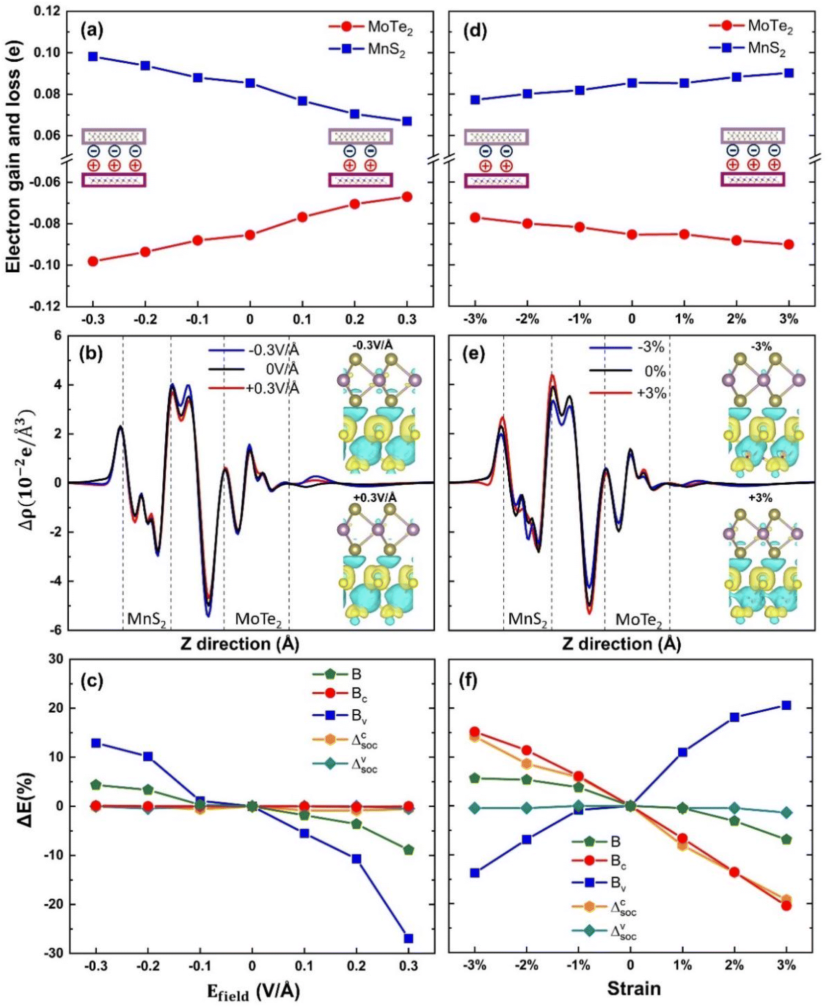 | ||
| Fig. 4 (a and d) The quantity of electrons gained and lost between MoTe2 and MnS2. (b and e) Planar differential charge density under different electric fields and strains; the top-right insets represent the differential charge density under the electric field of −0.3 V Å−1 and the strain of −3%; the bottom-right insets represent the differential charge density under the electric field of +0.3 V Å−1 and the strain of +3%. (c and f) The effective Zeeman field B, conduction band Zeeman field BC, valence band Zeeman field BV of the MoTe2/MnS2 heterostructure, and the conduction band spin splitting Ecsoc and valence band spin splitting Evsoc induced by the SOC of monolayer MoTe2. | ||
In order to figure out the conclusions that the applied electric field and the strain appear differently we performed the following analysis. It is well known that the valley Zeeman splitting phenomenon is a result of the combined interaction of SOC and magnetic fields. Fig. 4c shows the variation rates of the effective Zeeman field B, conduction band Zeeman field BC, valence band Zeeman field BV of MoTe2/MnS2 heterostructures and conduction band spin splitting Δcsoc, valence band spin splitting Δvsoc of monolayer MoTe2, under applied electric fields. Upon applying the electric field, the valence band Zeeman field BV exhibits a decreasing trend from −0.3 V Å−1 to +0.3 V Å−1, while the conduction band Zeeman field BC remains unchanged. The influence of the applied electric field on the spin splitting of the monolayer MoTe2 was found to be minimal. As mentioned above, as depicted in Fig. 3b, the magnetic moment of Mo also exhibited a decreasing trend with the electric field. This indicates that the change of magnetic moment primarily affects the BV, which leads to a decrease in the Zeeman field B and a corresponding decrease in the valley splitting.
In Fig. 4f, we examine the effects of different strain conditions on the variation rates of the effective Zeeman field B, conduction band Zeeman field BC, valence band Zeeman field BV of MoTe2/MnS2 heterostructures and conduction band spin splitting Δcsoc, and valence band spin splitting Δvsoc of monolayer MoTe2. We observe that the change in BV follows an increasing trend from −3% to 3%, akin to the variation in the magnetic moment of Mo depicted in Fig. 3e. The changes of BC and Δcsoc show the same downward trend, which indicates that the strain leads to the decrease of spin splitting of monolayer MoTe2, so also it leads to the decrease of conduction band splitting after the formation of heterostructure; Δvsoc remains relatively constant. This suggests that BV is primarily influenced by the magnetic moment, while strain affects the extent of SOC in the conduction band. Considering the opposing trends of BC and BV, the overall variation of the Zeeman field B demonstrates a decrease, indicating that the change in BC is more significant than in BV. Hence, we propose that the mechanisms underlying the influence of electric fields and strain on valley splitting are distinct. The modulation of valley splitting by the electric field is due to a direct influence on the MPE between the interfaces leading to a change in the Mo atomic magnetic moment, causing a change in the Zeeman splitting field in the valence band. Similarly, we define strains as the strain field, which affects not only the MPE between the interfaces leading to a change in the Zeeman splitting field in the valence band, but also the spin splitting caused by the SOC of MoTe2 itself, leading to a change in the Zeeman splitting field in the conduction band, and thus the magnitude of the valley splitting is modulated by the combined influence of the two factors.
4. Conclusions
In this study, we employed first-principles calculations to show the large valley splitting induced in monolayer MoTe2 when interfaced with ferromagnetic monolayer MnS2. The results revealed a substantial intrinsic valley splitting in the MoTe2/MnS2 heterostructure, reaching up to 55.3 meV, which corresponds to the magnitude of splitting induced by the external magnetic field of 476 T. Moreover, we demonstrate the tunable valley splitting through the application of electric fields and biaxial strains. Under electric field conditions, the valley splitting can be finely adjusted within the range of 49.2 to 56.6 meV, while the biaxial strains allow modulation from 50.8 to 57.4 meV. Therefore, the MoTe2/MnS2 heterostructure is a potential candidate material for valley electronics with strong valley splitting properties, presenting significant potential for applications in valley electronic devices. Furthermore, the Berry curvature is also influenced by different electric fields or strains. Additionally, we observed the influence of electric fields and strains on Berry curvature, with the difference in Berry curvature decreasing under varying electric fields (−0.3 V Å−1 to +0.3 V Å−1) and increasing under biaxial strains (−3% to 3%). According to our study, we also found that the two modes of action, applied electric field and strain, have different mechanisms for regulating the valley splitting of MoTe2. The electric field affects the MPE leading to a change in the distribution of electric dipoles at the interface, which in turn affects the induced magnetic moments of the Mo atoms leading to a change in the valley splitting. Biaxial strain affects not only the MPE at the interface, but also the intrinsic spin splitting due to the SOC of the monolayer MoTe2 itself, and these two factors jointly influence the change of valley splitting, even the latter being the main influence mechanism.Conflicts of interest
There are no conflicts to declare.Acknowledgements
We are grateful for the support of the National Natural Science Foundation of China (NSFC, Grant No. 51902033, 62175021), the China Postdoctoral Science Foundation (Grant No. M2020683282), the Sichuan Provincial Science and Technology Department (Grant No. 99203070) the Scientific Research Foundation of Chengdu University of Information Technology (Grant No. KYTZ202006, KYQN202312), and the College student Innovation Project (Grant No. 202210621239).References
- M. Ezawa, Phys. Rev. Lett., 2012, 109, 5 CrossRef PubMed.
- M. Tahir, A. Manchon, K. Sabeeh and U. Schwingenschlogl, Appl. Phys. Lett., 2013, 102, 4 CrossRef.
- C. J. Tabert and E. J. Nicol, Phys. Rev. B: Condens. Matter Mater. Phys., 2013, 87, 7 Search PubMed.
- W. Yao, D. Xiao and Q. Niu, Phys. Rev. B: Condens. Matter Mater. Phys., 2008, 77, 7 Search PubMed.
- B. Van Duppen, P. Vasilopoulos and F. M. Peeters, Phys. Rev. B: Condens. Matter Mater. Phys., 2014, 90, 10 CrossRef.
- C. J. Tabert and E. J. Nicol, Phys. Rev. B: Condens. Matter Mater. Phys., 2014, 89, 9 CrossRef.
- M. Mirzaei, T. Vazifehshenas, T. Salavati-fard, M. Farmanbar and B. Tanatar, Phys. Rev. B, 2018, 98, 9 CrossRef.
- D. Oliveira, L. Villegas-Lelovsky, M. A. G. Soler and F. Y. Qu, Phys. Rev. B, 2018, 97, 12 Search PubMed.
- Y. Ye, J. Xiao, H. L. Wang, Z. L. Ye, H. Y. Zhu, M. Zhao, Y. Wang, J. H. Zhao, X. B. Yin and X. Zhang, Nat. Nanotechnol., 2016, 11, 597–602 CrossRef PubMed.
- M. Q. Sui, G. R. Chen, L. G. Ma, W. Y. Shan, D. Tian, K. Watanabe, T. Taniguchi, X. F. Jin, W. Yao, D. Xiao and Y. B. Zhang, Nat. Phys., 2015, 11, 1027–1031 Search PubMed.
- M. Kim, J. H. Choi, S. H. Lee, K. Watanabe, T. Taniguchi, S. H. Jhi and H. J. Lee, Nat. Phys., 2016, 12, 1022–1026 Search PubMed.
- N. Cortes, O. Avalos-Ovando, L. Rosales, P. A. Orellana and S. E. Ulloa, Phys. Rev. Lett., 2019, 122, 6 CrossRef PubMed.
- K. F. Mak, K. L. He, J. Shan and T. F. Heinz, Nat. Nanotechnol., 2012, 7, 494–498 CrossRef CAS PubMed.
- A. Srivastava, M. Sidler, A. V. Allain, D. S. Lembke, A. Kis and A. Imamoglu, Nat. Phys., 2015, 11, 141–147 Search PubMed.
- Q. Y. Zhang, S. Y. A. Yang, W. B. Mi, Y. C. Cheng and U. Schwingenschlogl, Adv. Mater., 2016, 28, 959–966 CrossRef CAS PubMed.
- Y. C. Cheng, Q. Y. Zhang and U. Schwingenschlogl, Phys. Rev. B: Condens. Matter Mater. Phys., 2014, 89, 15 Search PubMed.
- W. Hu and J. L. Yang, Comput. Mater. Sci., 2016, 112, 518–526 CrossRef CAS.
- R. Mas-Balleste, C. Gomez-Navarro, J. Gomez-Herrero and F. Zamora, Nanoscale, 2011, 3, 20–30 RSC.
- S. A. Vitale, D. Nezich, J. O. Varghese, P. Kim, N. Gedik, P. Jarillo-Herrero, D. Xiao and M. Rothschild, Small, 2018, 14, 15 Search PubMed.
- D. Xiao, G. B. Liu, W. X. Feng, X. D. Xu and W. Yao, Phys. Rev. Lett., 2012, 108, 5 Search PubMed.
- L. Xu, M. Yang, L. Shen, J. Zhou, T. Zhu and Y. P. Feng, Phys. Rev. B, 2018, 97, 6 Search PubMed.
- G. Aivazian, Z. R. Gong, A. M. Jones, R. L. Chu, J. Yan, D. G. Mandrus, C. W. Zhang, D. Cobden, W. Yao and X. Xu, Nat. Phys., 2015, 11, 148–152 Search PubMed.
- H. L. Zeng, J. F. Dai, W. Yao, D. Xiao and X. D. Cui, Nat. Nanotechnol., 2012, 7, 490–493 CrossRef CAS PubMed.
- J. Kim, X. P. Hong, C. H. Jin, S. F. Shi, C. Y. S. Chang, M. H. Chiu, L. J. Li and F. Wang, Science, 2014, 346, 1205–1208 CrossRef CAS PubMed.
- E. J. Sie, J. McIver, Y. H. Lee, L. Fu, J. Kong and N. Gedik, Nat. Mater., 2015, 14, 290–294 CrossRef CAS PubMed.
- J. S. Qi, X. Li, Q. Niu and J. Feng, Phys. Rev. B: Condens. Matter Mater. Phys., 2015, 92, 5 Search PubMed.
- C. Zhao, T. Norden, P. Y. Zhang, P. Q. Zhao, Y. C. Cheng, F. Sun, J. P. Parry, P. Taheri, J. Q. Wang, Y. H. Yang, T. Scrace, K. F. Kang, S. Yang, G. X. Miao, R. Sabirianov, G. Kioseoglou, W. Huang, A. Petrou and H. Zeng, Nat. Nanotechnol., 2017, 12, 757–762 CrossRef CAS PubMed.
- X. Liang, L. J. Deng, F. Huang, T. T. Tang, C. T. Wang, Y. P. Zhu, J. Qin, Y. Zhang, B. Peng and L. Bi, Nanoscale, 2017, 9, 9502–9509 RSC.
- T. Norden, C. Zhao, P. Y. Zhang, R. Sabirianov, A. Petrou and H. Zeng, Nat. Commun., 2019, 10, 10 CrossRef PubMed.
- Y. Song, Q. Zhang, W. B. Mi and X. C. Wang, Phys. Chem. Chem. Phys., 2016, 18, 15039–15045 RSC.
- Y. Song, X. C. Wang and W. B. Mi, Adv. Electron. Mater., 2017, 3, 7 Search PubMed.
- D. Zhong, K. L. Seyler, X. Y. Linpeng, R. Cheng, N. Sivadas, B. Huang, E. Schmidgall, T. Taniguchi, K. Watanabe, M. A. McGuire, W. Yao, D. Xiao, K. M. C. Fu and X. D. Xu, Sci. Adv., 2017, 3, 6 Search PubMed.
- F. K. Deng, J. H. Wei, Y. D. Xu, Z. Q. Lin, X. Lu, Y. J. Wan, R. Sun, C. P. Wong and Y. G. Hu, Nano-Micro Lett., 2023, 15, 106 CrossRef CAS PubMed.
- W. F. Cai, J. Y. Wang, Y. M. He, S. Liu, Q. H. Xiong, Z. Liu and Q. Zhang, Nano-Micro Lett., 2021, 13, 74 CrossRef PubMed.
- K. L. Seyler, D. Zhong, B. Huang, X. Y. Linpeng, N. P. Wilson, T. Taniguchi, K. Watanabe, W. Yao, D. Xiao, M. A. McGuire, K. M. C. Fu and X. D. Xu, Nano Lett., 2018, 18, 3823–3828 CrossRef CAS PubMed.
- M. Kan, S. Adhikari and Q. Sun, Phys. Chem. Chem. Phys., 2014, 16, 4990–4994 RSC.
- D. J. O'Hara, T. C. Zhu, A. H. Trout, A. S. Ahmed, Y. K. Luo, C. H. Lee, M. R. Brenner, S. Rajan, J. A. Gupta, D. W. McComb and R. K. Kawakami, Nano Lett., 2018, 18, 3125–3131 CrossRef PubMed.
- X. L. Xu, Y. Pan, S. Liu, B. Han, P. F. Gu, S. H. Li, W. J. Xu, Y. X. Peng, Z. Han, J. Chen, P. Gao and Y. Ye, Science, 2021, 372, 195–200 CrossRef CAS PubMed.
- I. G. Lezama, A. Ubaldini, M. Longobardi, E. Giannini, C. Renner, A. B. Kuzmenko and A. F. Morpurgo, 2D Mater., 2014, 1, 021002 CrossRef CAS.
- C. Ruppert, O. B. Aslan and T. F. Heinz, Nano Lett., 2014, 14, 6231–6236 CrossRef CAS PubMed.
- G. Kresse and J. Furthmuller, Phys. Rev. B: Condens. Matter Mater. Phys., 1996, 54, 11169–11186 CrossRef CAS PubMed.
- J. P. Perdew, K. Burke and M. Ernzerhof, Phys. Rev. Lett., 1996, 77, 3865–3868 CrossRef CAS PubMed.
- D. Chen, C. L. Wang, J. J. Li and F. F. Liu, J. Magn. Magn. Mater., 2022, 563, 169966 CrossRef CAS.
- J. T. Guan, C. X. Huang, K. M. Deng and E. J. Kan, J. Phys. Chem. C, 2019, 123, 10114–10119 CrossRef CAS.
- L. Wang, T. Maxisch and G. Ceder, Phys. Rev. B: Condens. Matter Mater. Phys., 2006, 73, 6 Search PubMed.
- C. Ling and F. Mizuno, Chem. Mat., 2012, 24, 3943–3951 CrossRef CAS.
- M. Kan, J. Zhou, Q. Sun, Y. Kawazoe and P. Jena, J. Phys. Chem. Lett., 2013, 4, 3382–3386 CrossRef CAS PubMed.
- S. L. Dudarev, G. A. Botton, S. Y. Savrasov, C. J. Humphreys and A. P. Sutton, Phys. Rev. B: Condens. Matter Mater. Phys., 1998, 57, 1505–1509 CrossRef CAS.
- N. Marzari, A. A. Mostofi, J. R. Yates, I. Souza and D. Vanderbilt, Rev. Mod. Phys., 2012, 84, 57 CrossRef.
- A. A. Mostofi, J. R. Yates, Y. S. Lee, I. Souza, D. Vanderbilt and N. Marzari, Comput. Phys. Commun., 2008, 178, 685–699 CrossRef CAS.
- H. S. Zhang, W. J. Yang, Y. H. Ning and X. H. Xu, Phys. Rev. B, 2020, 101, 9 Search PubMed.
- C. M. Ke, Y. P. Wu, W. H. Yang, Z. M. Wu, C. M. Zhang, X. Li and J. Y. Kang, Phys. Rev. B, 2019, 100, 6 CrossRef.
- D. J. Thouless, M. Kohmoto, M. P. Nightingale and M. den Nijs, Phys. Rev. Lett., 1982, 49, 405–408 CrossRef CAS.
- Y. Yao, L. Kleinman, A. H. MacDonald, J. Sinova, T. Jungwirth, D.-S. Wang, E. Wang and Q. Niu, Phys. Rev. Lett., 2004, 92, 037204 CrossRef PubMed.
- Z. Y. Zhang, M. S. Si, Y. H. Wang, X. P. Gao, D. Sung, S. Hong and J. He, J. Chem. Phys., 2014, 140, 174707 CrossRef CAS PubMed.
- C. X. Wang, B. Fu and Y. K. An, Phys. E, 2022, 136, 9 CrossRef.
- M. Abdollahi and M. B. Tagani, J. Phys.: Condens.Matter, 2022, 34, 12 Search PubMed.
- G. Yang, J. Li, Z. Liu, C. C. Li and X. J. Mao, Phys. Chem. Chem. Phys., 2019, 21, 15151–15156 RSC.
Footnote |
| † Electronic supplementary information (ESI) available. See DOI: https://doi.org/10.1039/d4ra01013b |
| This journal is © The Royal Society of Chemistry 2024 |