
 Open Access Article
 This Open Access Article is licensed under a
 Creative Commons Attribution 3.0 Unported Licence
Investigation of optical, dielectric, and conduction mechanism in lead-free perovskite CsMnBr3†
Moufida Krimia,
Fadhel Hajlaouib,
Mohammed S. M. Abdelbakycd,
Santiago Garcia-Grandad and
Abdallah Ben Rhaiem *a
*a
aLaboratory LaSCOM, Faculty of Sciences of Sfax, University of Sfax, BP1171, 3000, Sfax, Tunisia. E-mail: abdallahrhaiem@yahoo.fr
bLaboratoire Physico-chimie de l’Etat Solide, D'epartement de Chimie, Facult'e des Sciences de Sfax, Universit'e de Sfax, B.P. 1171, 3000 Sfax, Tunisia
cDepartment of Physical Chemistry, Faculty of Chemical Sciences, University of Salamanca, E-37008 Salamanca, Spain
dDepartment of Physical and Analytical Chemistry, Faculty of Chemistry, University of Oviedo-CINN(CSIC), 33006 Oviedo, Spain
First published on 27th March 2024
Abstract
Metallic perovskites have advantageous optical and electrical properties, making them a valuable class of semiconductors for the manufacturing of solar cells. CsMnBr3 is notable among them due to its important optical characteristics. The electrical and dielectric characteristics as a semiconductor are examined in this study. Direct transitions with a 3.29 eV bandgap and an Urbach energy of 0.96 eV are revealed by the results. Through AC conductivity, it demonstrated semiconductor characteristics at 443 K. The dielectric loss varied with frequency and peaked at high frequencies. Furthermore, as temperature rose, a relaxation peak in the electrical modulus was seen to migrate to higher frequencies. Ac conductivity is described by the double power law expression. The conduction in our compound is governed by small polaron tunneling. Based on the optical results reported in the bibliography for this sample, we realize the importance of examining the electrical characteristics to comprehend the semiconductor behavior of CsMnBr3.
1. Introduction
Perovskite-based solar cells, especially those containing lead-free metal halides, have significantly improved their energy efficiency, jumping from 3.8% in 2009 to 25.7% in 2022.1 However, the use of these materials is strictly regulated due to their harmful effects on human and animal health, as well as the environment, and their long-term instability. To tackle these challenges, the design of stable lead-free perovskites is a promising approach. These alternative materials have shown great potential for various green energy applications, including photovoltaic solar cells. Many researchers have focused on the fabrication and study of the optical/optoelectronic properties of halogenated metal perovskites, as they play a crucial role in the efficiency of electrical and optoelectronic devices by facilitating charge transport. Many researchers have focused on studying the optical/optoelectronic properties of metal halide perovskite materials, which are crucial for the efficiency of electrical and optoelectronic devices due to their role in charge transport. The optical properties of metal halide perovskites have been found to be highly tunable, making them attractive for a wide range of applications in photovoltaics, light-emitting diodes, and photodetectors.2–4 Researchers have been investigating ways to enhance the absorption and emission properties of these materials, as well as improve their stability and performance under different environmental conditions. Additionally, the understanding of charge transport mechanisms in metal halide perovskites is crucial for the development of efficient electronic devices with high conductivity and low recombination rates. However, there is still a lack of complete understanding regarding the electrical transport mechanism and dielectric behavior. Mohammed et al.5,6 conducted a study in this area, uncovering that metal halide perovskite demonstrates a significant dielectric constant with minimal dielectric loss. The CsSnCl3 compound exhibits a dielectric constant of 104, surpassing that of MCdCl3 (M = CH3NH3, (CH3)2NH2), which is at 103. This variation in dielectric properties is also reflected in the difference in electrical conductivity (10−2 Ω cm−1 for CsSnCl3 and 10−4 Ω cm−1for MCdCl3).5,6 These materials have a significant energy storage capacity per unit volume due to their high dielectric constant. Additionally, their low dielectric loss (<0.1) allows them to store energy for long periods. These characteristics make them potentially interesting materials for energy recovery devices, like high-performance capacitors or energy storage systems for electronic applications. Further research in this area could provide valuable insights into the underlying mechanisms governing the unique dielectric and electric behavior of metal halide perovskites, ultimately leading to the development of advanced electronic devices with enhanced performance characteristics. CsMnBr3 is a well-studied compound in the realm of optoelectronic devices. This perovskite specimen displays notably short radiative lifetimes (in the picosecond range) and a high photoluminescence quantum yield (PLQY) of 54%, emitting a red photoluminescence response.7 In addition, CsMnBr3 exhibits stronger electronic and longitudinal optical phonon coupling strength than that of NCs at low temperatures. SC has a strong saturable absorption property, with a modulation depth of approximately 27%. Interestingly, the SC also exhibits a large two-photon absorption coefficient of about 0.035 cm GW−1 at 800 nm and excellent optical limiting behavior. The experimental results indicate that this material is a class of excellent eco-friendly optoelectronic materials.7 The lack of understanding surrounding the electric and dielectric properties of CsMnBr3 is the central focus of our investigation that's why our research is dedicated to exploring the electrical and dielectric traits of CsMnBr3.To achieve this goal, a series of experiments were carried out to analyze the conductivity and dielectric features of CsMnBr3 under various temperature and frequency conditions. Our results unveil intriguing patterns in the material's behavior, offering insights into its potential applications.
2. Experimental
2.1. Synthetic processes
The CsMnBr3 single crystal was obtained using a slow evaporation method. Briefly, 0.5 mmol (0.106 g) of CsBr and 1 mmol (0.224 g) of MnBr2 were added to the mixed solution of water and hydrobromic acid. The obtained solution is then stirred at a temperature of 120 °C for one hour then the mixture is allowed to evaporate at room temperature. After being stored for 5 days, a polycrystalline material with white crystal of mm size was formed as shown in Fig. (S1).†2.2. Equipment
The purity of the compounds is checked using X-ray powder diffraction at the ambient temperature with CuKα radiation (λ = 1.5406 A, 10° ≤ 2θ ≤ 80°). Furthermore, UV-visible spectroscopy was utilized to analyze the optical characteristics of the material under investigation. The analysis was conducted on a 1 mm thick pellet employing the “UV-3101PC” within the wavelength range of 200–800 nm. The electrical impedance of a silver-covered pellet, 1 mm thick with an 8 mm surface area, was measured across temperatures ranging from 363 K to 473 K and frequencies from 0.1 to 10 million Hertz using a “Solartron1260” device. To enhance accuracy, the pellet was coated with a layer of silver. The measurement involved utilizing two thin copper wires with silver paint for electrical contacts on the pellet's surface. This setup allowed for impedance measurements within a specific temperature and frequency range, ensuring precise data collection.3. Result and discussion
3.1. X-Ray diffraction
The final result for X-ray Rietveld refinement of the powdered sample of our compound is presented in Fig. 1. As shown the observed data matches with the expected diffraction patterns and unit cell parametersobtained from DICVOL indexing, Le Bail fitting, and the Rietveld refinement using FULLPROF in WinPLOTR, emphasizing the strong evidence supporting the presence of the title compound as the sole phase within the analyzed batch.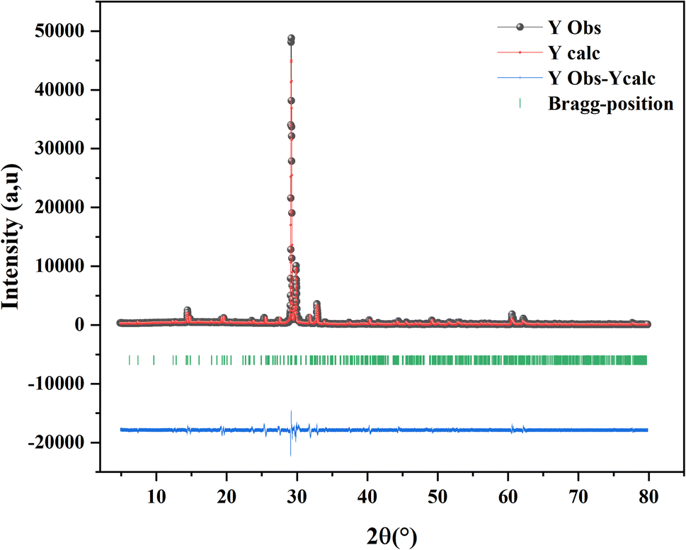 | ||
| Fig. 1 The X-ray pattern of CsMnBr3 powdered sample. | ||
The obtained phase was fully indexed in the P63/mmc space group of the hexagonal crystal structure (JCPDS No. 26-0387). The unit cell parameters as well as the fit criteria are reported in the following table:
The crystal structure of CsMnBr3consist of linear chains of distorted face-sharing [MnBr6]octahedron with a D3d symmetry parallel to the c-axis that are bridged by Cs ions, this later is bound to twelve equivalent Br− atoms to generate CsBr12 cuboctahedra. These cuboctahedra share corners with six others equivalent CsBr12 cuboctahedra, faces with eight others equivalent CsBr12 cuboctahedra, and faces with six others equivalent MnBr6 octahedra. In CsBr12 there are six long Cs–Br bonds of length 3.98 (1) Å and six short bonds of length 3.83 (2) Å. In this material the Mn–Br bonds are shorter than those of Cs–Br which are of the order of 2.69 (3) Å.8,9
As seen in Fig. 2, the compound forms chains of face-sharing octahedral composed of manganese surrounded by six bromine atoms [MnBr6], those atoms are arranged in a manner creating extended chains along the crystallographic c-axis.The arrangement of cesium ions between the [MnBr6] chains ensures the overall charge neutrality of the crystal lattice. This ionic arrangement stabilizes the structure, preventing excess positive or negative charges within the unit cell. The chains of [MnBr6] octahedra, along with the cesium ions, are interconnected in three dimensionsresulting in a networked structure.
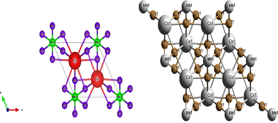 | ||
| Fig. 2 Schematic representation of the CsMnBr3 structure. | ||
3.2. Optical properties
UV-visible spectroscopy is a technique used to analyze how molecules interact with light in the UV and visible regions of the electromagnetic spectrum. It provides information about the electronic transitions and absorption of light by molecules, offering insights into their chemical structure, concentration, and properties. This study is employed to estimate the band gap of materials, especially semiconductors or insulators, by analyzing their absorption spectra. The band gap represents the energy difference between the valence band (highest energy level filled with electrons) and the conduction band (lowest energy level with no electrons) in a material's electronic structure. Also, this measurement serves to the calculation of the absorption coefficient (α) which allows us to study the optically induced transition and to better understand the band structure of ourmaterial.To investigate the optical properties of CsMnBr3 compound, we recorded the absorbance spectra in the UV-visible region 200–900 nm at room temperature. Fig. 3 illustrates the absorbance spectrum versus wavelength of the obtained device. In ultra-violet range, (λ < 400 nm), we notice the presence of an absorption band at λ = 326 nm was attributed to the ligand–metal transition (LMCT) of the perovskite sample.10 In fact, CsMnBr3 consists of cesium cations (Cs+) and manganese(III) ions (Mn3+) that are coordinated with bromine ions (Br−) in a crystal structure. The manganese ion is the transition metal in this compound, and the LMCT transitions would typically involve the interactions between the d orbitals of manganese and the p orbitals of bromine.11 Furthermore, in the wavelength higher than 400 nm, three main strong absorption peaks at 436 nm, 516 nm and 659 nm are depicted. Those peaks can be attributed to the electronic transition of Mn (3d).12 Those properties allow our compound to be used as a photo-catalysis material and photovoltaic solar cell.13
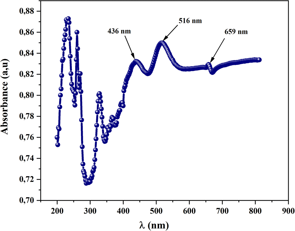 | ||
| Fig. 3 Absorbance spectrum of CsMnBr3 compound. | ||
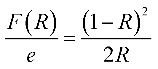
Reflectance spectrum can be used to calculate the optical band gap for such compound. This key parameter is essential for designing electronic devices. For instance, in solar cells or photodetectors, the band gap influences the absorption of light and the efficiency of converting photons into electrical energy. Accurate knowledge of the band gap helps optimize the design and performance of such devices. Calculate the optical band gap for CsMnBr3 compound is essential for applications in light-emitting diodes (LEDs), lasers, sensors, and other optical devices. In this work the calculation of the band gap (Eg) is done based on the Kubelka–Munk equation:14,15
With n is a number that identifies the type of the transition. Where n = 1/2 for an indirect allowed transition, n = 2 for an allowed direct transition, n = 2/3 for direct forbidden transition and finally n = 1/3 for indirect forbidden transition.16 Fig. 4a shows the dependence of (F(R) × hν2) and (F(R) × hν1/2) on the energy (hν) curves for the CsMnBr3 compound.
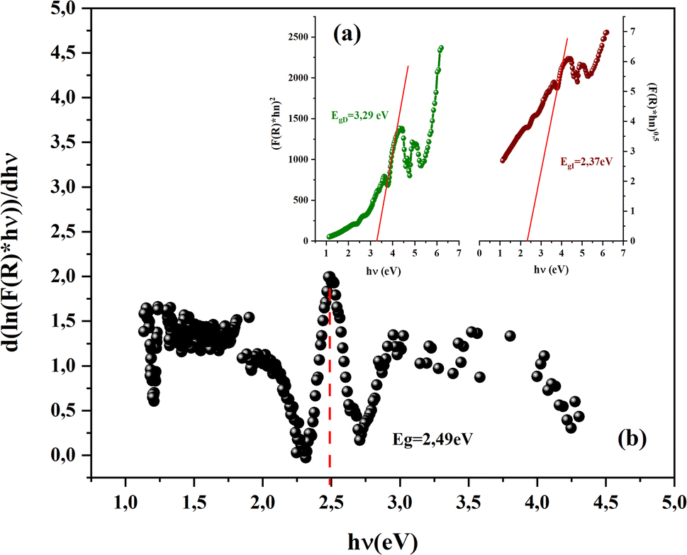 | ||
| Fig. 4 (a and b): a dependence of (F(R) × hν2) and (F(R) × hν1/2) on the energy (hν). | ||
After extrapolating the linear sections of these graphs to the energy axis, the energy value at (F(R) × hv)n = 0 provides the values of the energy gap, Egd = 3.29 eV and Egin = 2.37 eV. The obtained band gap values were included in the range band gap semiconductors which confirm the importance of our sample for several applications.
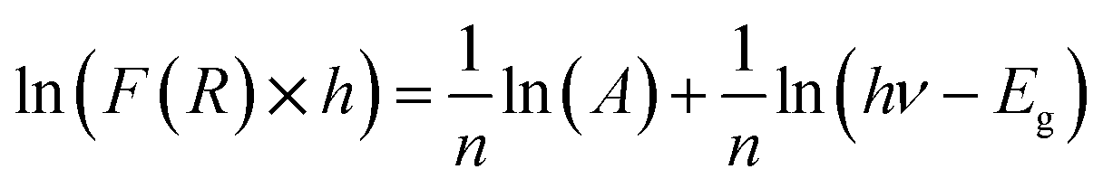
Using the logarithmic derivative (LD) we can recalculate the band gap energy there by identifying the transition mode of our studied compound.17 LD transformation starts from the modified Kubelka–Munk equation. For the sake of calculating the natural logarithm, let us suppose that all the quantities in the previous expression are unitless then the natural logarithm will be:
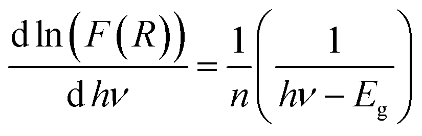
We use the experimental data to calculate the left side of this equation. Drawing the curve of (d![[thin space (1/6-em)]](https://www.rsc.org/images/entities/char_2009.gif) ln(F(R))/dhν) vs. (hν), we can accurately determine the optical band gap value (Fig. 4b). A peak indicates the band gap value of 2.49 eV, which closely aligns with the calculated value of 2.37 eV obtained by extrapolating the Kubelka–Munk expression for the indirect allowed transition.
ln(F(R))/dhν) vs. (hν), we can accurately determine the optical band gap value (Fig. 4b). A peak indicates the band gap value of 2.49 eV, which closely aligns with the calculated value of 2.37 eV obtained by extrapolating the Kubelka–Munk expression for the indirect allowed transition.
In a semiconductor or insulating material, the absorption edge typically displays a rapid increase in absorption at photon energies near or above the band gap energy. Beyond this edge, in the tail region of the absorption spectrum, there exists an exponential increase in absorption, often referred to as the Urbach tail. The Urbach tail represents the localized states in the band gap of the material caused by defects, impurities, or structural disorder.18 Empirically, Urbach tail Eucan be obtained using the Urbach–Martienssen law presented by the following expression:
We notice that they obtained Urbach-energy (0.96 eV) present only 30% from the band gap energy which indicates a narrower distribution of localized states within the band gap (Fig. 5). This implies lower disorder, fewer defects and reduced structural imperfections within CsMnBr3 material. The Urbach energy can be more exploited using the following expression:
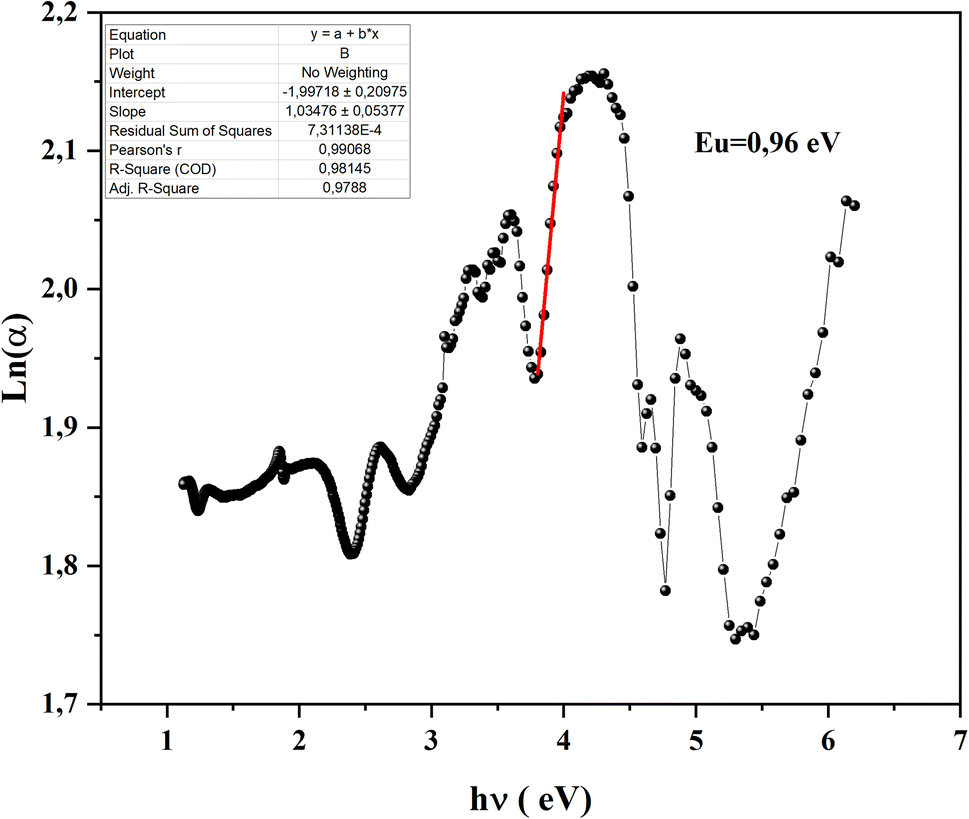 | ||
| Fig. 5 Ln (α) as a function of (hα (ev)) for CsMnBr3 perovskite sample. | ||
The estimated values of electron–phonon interaction strength (Ee–ph) are close to 24.7 eV.
3.3. Electrical properties
3.3.1.1 AC conductivity. AC-conductivity as a function of temperature for the CsMnBr3 sample for selected values of frequency is depicted in Fig. 6a. Obviously, the AC conductivity of the compound studied increases then decreases as the temperature varies. Besides, a semiconductor–metal transition21 takes place at around TSM = 423 K. Noticeably, the variation below TSM reflects a semiconductor behavior, while that above TSM exhibits metallic behavior. This change in behavior of the conductivity can be due to several factors. Generally, the increase in conductivity with increasing temperature is attributed to the thermally activated charge carrier. In fact, the ionic conductivity of perovskite sample depends on the rate and mobility of charge carriers.22 As the temperature increases, traps within the material start to release charge carriers, indeed, with an increase in temperature, the traps (defects and grain boundary) become less effective at holding onto the charge carriers, causing them to be released, increasing the free charge carrier, and contributing to the material's conductivity. However, for such temperature called TSM this emission stop, when all the trapped charges become free leading to saturation in the conductivity process before it starts to decrease with increasing temperatures. This decrease can be explained by the fact that the conductivity depends on the density of available free charge carriers. Some of these carriers might get stuck or trapped at defects in the grain boundaries of the material. Additionally, the movement of these carriers can be affected by vibrations in the lattice, caused by phonons. These vibrations can limit the carrier's ability to move freely, thereby reducing the overall conductivity.
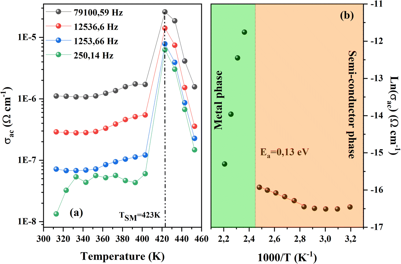 | ||
| Fig. 6 (a) Ac conductivity vs. temperature for CsMnBr3 perovskite sample. (b) Variation of ln(σac) as a function of 1000/T. | ||
To investigate the effect of the observed transition in the activation energy for the studied compound we fitted the obtained curves of σac for a fixed value of frequency (12536.6 Hz) using the Arrhenius expression as depicted in Fig. 6b.
The observed linear variation in the Arrhenius plot reveals that the observed semiconductor–metal transition is temperature-activated. This transition is filled by a leap in activation energy; the increase in activation energy shows a noticeable shift in the material's conducting qualities as temperature increases. The lower activation energy of 0.13 eV in the semiconductor state indicates that charge carriers can easily pass over the energy band gap, contributing to the material's semiconductor-like characteristics. However, as the temperature increase the conductivity decreases indicating a change toward metallic behavior.
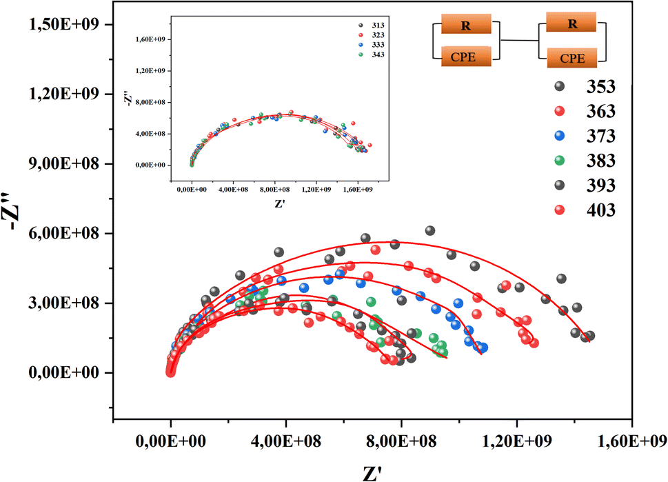
3.3.2.1 Impedance spectroscopy (CIS). Impedance spectroscopy is a powerful tool for studying the electrical behavior of materials under different conditions and frequencies, providing valuable insights into their performance, and enabling the optimization of various technologies and systems. The contribution of electrodes, grain boundaries and grains to charge transport in the material can be differentiated through the complex impedance study. The frequency dependence of the complex impedance is illustrated by the following equation:
| Z(ω) = Z′(ω) − jZ′′(ω) |
To better differentiate the existing contributions in the material, we draw Nyquist diagrams as shown in Fig. 7.
 | ||
| Fig. 7 Nyquist diagram of CsMnBr3 perovskite sample. | ||
The analysis of these diagrams clearly shows that the curves showing the variation of (−Z′′) as a function of (Z′) are centered below the axis of the real of impedance, therefore the conduction of this material does not obey the Debye model, but it follows the Cole–Cole model.23 As shown in the inset of Fig. 7 at low temperatures (T < 353 K) CsMnBr3 compound show only slight variations in impedance, which may be the result of different factors like slow electrode kinetics, limited ion mobility, or reduced system reactivity for that range of temperatures. For temperature greater than 353 K the radius of the semicircles decreases with increasing temperature indicating that the temperature coefficient of resistivity is negative.24 This proves that the CsMnBr3 compound possess semi-conductive properties and also that the conduction process is thermally activated. The best fit is obtained when employing an equivalent circuit composed by two cellules each one of them modelized by a parallel combination of resistance and fractal capacitance. The semicircle seen at lower frequencies in the impedance spectra illustrate the response of the grain boundaries when the one observed for high values of frequency characterizes the electrical response of the grain. The frequency dependence of Z′ and Z′′ are shown in Fig. (S2) and (S3).† The strong agreement or good conformity observed between the calculated lines and experimental data suggests that the proposed or suggested equivalent circuit provides a reasonably accurate description of the crystal–electrolyte interface. From the fitted data, specific parameters such as the resistance of both the grain and grain boundary can be extracted. The acquired values of grain and grain boundary resistances as a function of temperature showed in Fig. 8 reveal that the strength of the grains and grain borders diminishes as temperature increases, confirming the previously described negative thermal coefficient of resistance (NTCR) behavior. This behavior is confirmed by the observed decrease in grain and grain boundary resistances with increasing temperature, which can be attributed to many factors such as grain boundary thermal conductivities, grain size effects, thermal resistance and conductance of tilt grain boundaries, and microscale imaging of thermal conductivity suppression.25
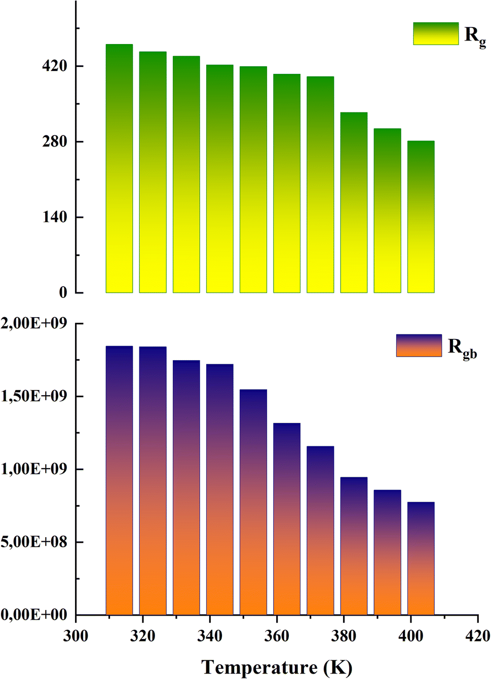 | ||
| Fig. 8 Variation in the strength of the grains and grain boundaries of the CsMnBr3 compound. | ||
By comparing the obtained values of resistance for both grain and grain boundary we notice that the resistance associated with the grain is much lower than the resistance associated with the grain boundary, it indicates that the grain is the primary governing species of conductivity. In this case, the decreased resistance in the grain area suggests that charge carriers can pass more freely through the bulk material (grains) rather than being hampered by interfaces or flaws in the grain boundaries.26
3.3.2.2 Dielectric permittivity and modulus studies. This compound's dielectric response can be computed using the following formula:
| ε(ω) = ε′(ω) + jε′′(ω) |
The real part, denoted by ε′(ω), corresponds to the energy stored by the system and ε′′ the imaginary component of the equation reflects the energy dissipation of the applied electric field, this have crucial roles in the process of ionic conduction within materials since it is influenced by four main types of polarization: interfacial, dipolar, electronic, and ionic.27 The theoretical adjustment of ε′′ can be done using several expressions, in our work we use the modified Cole–Cole model us follow:
We notice that the factor α increase with increasing temperature but not reaching the unity (α < 0.724) proving the existence of non-Debye relaxation. Also, the conductivity of free charge σfc increase with increasing temperature whiles the relaxation time decrease. To differentiate between the existed contributions in the material by unmasking the electrode effect we use the electrical modulus, indeed this technique is valuable because it offers insights into the relaxation dynamics and polarization mechanisms of materials. These studies help elucidate how materials respond to an applied electric field across a range of frequencies or temperatures. Being mainly the reciprocal of complex permittivity, the complex modulus expressed by the following expression:
As shown in the previous figure, the widths of the asymmetric peaks in the imaginary component of the electric modulus (M′′) as a function of frequency are somewhat larger than the Debye peaks. By raising the temperature, the maxima of these peaks move towards the high frequencies. The analysis performed with Bergman's equation validated all these facts:
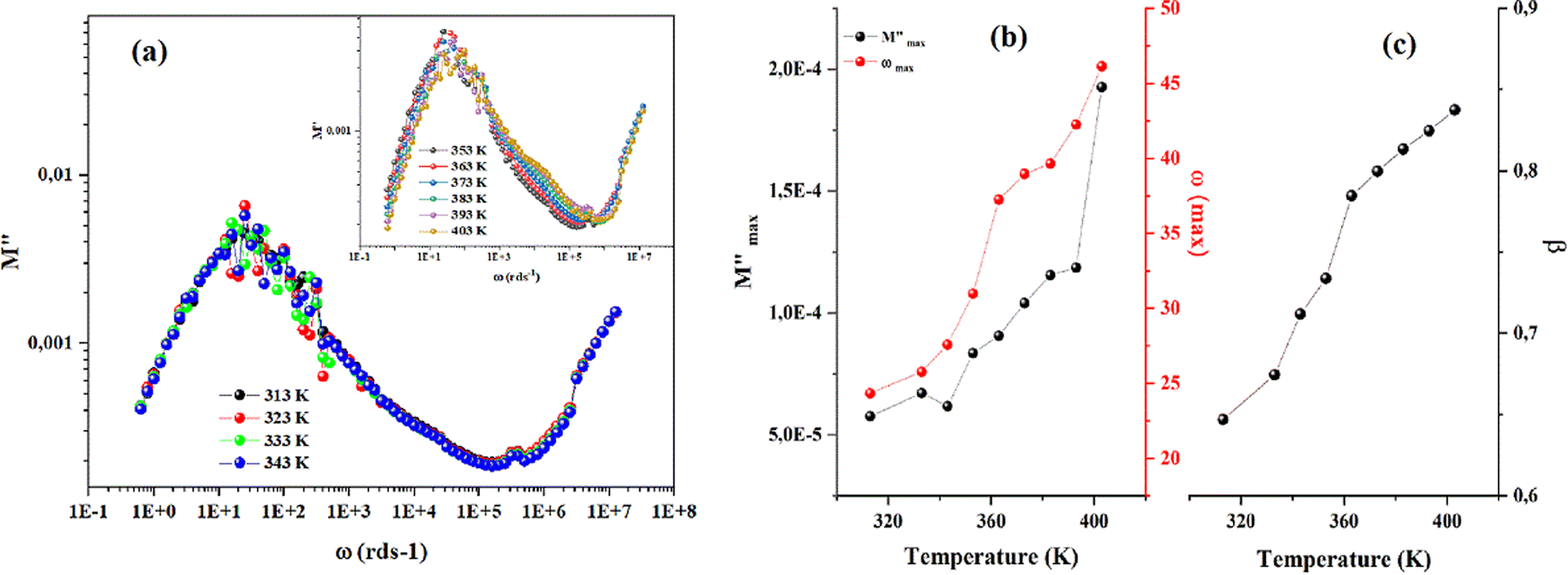 | ||
| Fig. 9 (a) Frequency variation of the imaginary part of complex modulus. (b) Temperature dependency of Bergman's parameter. | ||
3.3.2.3 AC conductivity. The frequency dependence of AC conductivity is depicted in Fig. 10. Three zones are seen by the conductivity curves. The first zone is associated with dc conductivity at low frequencies, whereas the second and third zones correspond to higher frequency values where the conductivity exhibits a dispersion effect, and each is defined by the terms (Aωs).
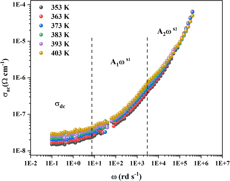 | ||
| Fig. 10 Frequency dependence of ac conductivity of CsMnBr3 compound. | ||
For such behavior the double power of Jonsher law is used with the following expression:
| σAC = σdc + A1ωs1 + A2ωs2 |
Were σdc is the pre-exponential factor, A1 and A2 are scaling coefficients that describe the amplitude of the frequency-dependent terms 0 < s1 < 1, which dominates at low frequencies and corresponds to short motion of the mobile ions. The third term corresponds to the high frequency dispersion region, where 1 < s2 < 2, that is associated with well localized hopping translational or re-orientational motion.29 As presented by Fig. (S6),† a good agreement between the theoretical and the experimental data was obtained which confirm our choice.
From the previous adjustment, the temperature dependency of σdc was obtained us depicted in Fig. 11a. The single slope of this curve indicates the presence of one single phase in the CsMnBr3 compound characterized by an activation energy Ea = 1.8 eV.
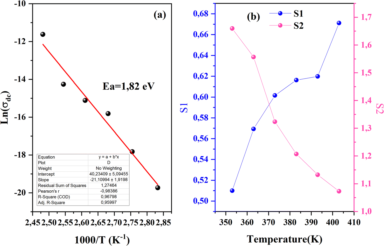 | ||
| Fig. 11 (a) Ln(σdc) vs. 1000/T of CsMnBr3 compound. (b) The exponent s1 and s2 of CsMnBr3 compound. | ||
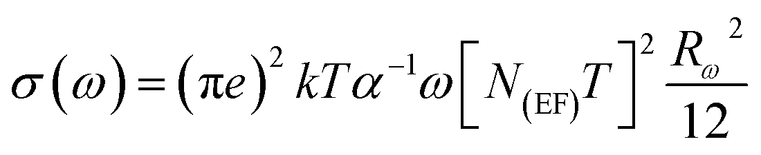
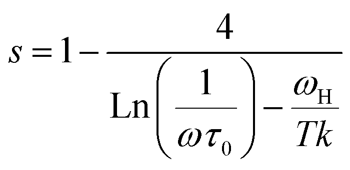
In order to identify the conduction mechanism, we plot the variation of the exponent s1 and s2 as a function of temperature in Fig. 11b, as presented, the increase in temperature leads to an increase in the values of s1 while the value of s2 decreases which suggest that the short motion of charge carriers dominates as the temperature increase.30 The temperature behavior of s1 is typically to that proposed by the non-small polaron tunneling model, for which the conductivity is given by the following expression:31
where ωH is the energy of polaron hopping. The power exponent is given by the expression:

These formulas are employed to adjust the swing of σac as a function of 1000/T for fixed frequency values. As demonstrated in Fig. (S6),† a good agreement was obtained between the empirical model and the experimental data confirming our model choice. The obtained parameters from this adjustment are classified in the Table (S2).†
We notice that an increase in frequency leads a decrease in the density of localized states which can be attributed to a change in the electronic state's energy distribution.32 Using the obtained value of ωH for different frequency values, we can calculate the tunneling distance for the SPT model given by the expression:
The tunneling distance never goes above 3.5 Å, being less than the interatomic distance, which confirms the dominance of small polaron tunneling. As the frequency increases, the recombination rates (R) and the recombination velocity (v) decrease, indicating faster lattice oscillations and energy loss. The effective distance that a small polaron may travel before its energy is dissipated is lowered by this energy dissipation, which decreases the tunneling distance (Fig. 12).33
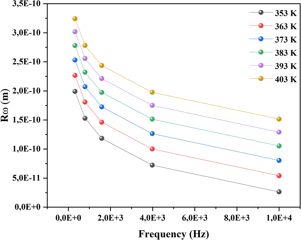 | ||
| Fig. 12 Frequency dependency of Rω of CsMnBr3 compound. | ||
4. Conclusion
CsMnBr3 single crystals with a P63/mmc space group crystallize in a hexagonal arrangement. According to optical investigation, our compound shows an indirect transition with a bandgap of 2.29 eV, and a disorder indicated by Urbach energy of 0.96 eV, making it a good device for optoelectronic applications. The AC conductivity's temperature dependence exhibits two distinct behaviors: for T < 443 K, the conductivity rises as the temperature increases, indicating a semi-conductive behavior; for T > 443 K, the conductivity falls as the temperature rises, exhibiting a typical metal behavior. An in-depth examination of the impedance data for T < 443 K reveals the grain contribution in addition to the grain boundary. The dielectric study proves that the real part of permittivity is thermally activated which means that increasing the temperature in fact increases the polarized dipoles. This result suggests that the prepared sample is a strong contender for application in FET devices as an active channel or dielectric gate. The frequency dependency of the electrical conductivity shows a double power law type nature. From this study we have demonstrate the NTCR behavior of our compound which leaves our compound compatible with applications based on the detection of infrared rays, also we have extracted the temperature dependency of the exponent S proving that the conduction is governed by the small polaron tunneling mechanism.Conflicts of interest
There are no conflicts to declare.Acknowledgements
Spanish Ministerio de Ciencia e Innovación (PID2020-113558RB-C41) and Gobierno del Principado de Asturias (GRUPIN-2021/50997) are acknowledged. The authors would be grateful to the Scientific and Technical Services (STSs) at the University of Oviedo for the instrumental support during this work. This work is also financed by the Tunisian Ministry of Higher Education and Scientific Research through funds granted to the research laboratories involved.References
- H. Su, Z. Xu, X. He, Y. Yao, X. Zheng, Y. She and S. Liu, Surface energy engineering of buried interface for highly stable perovskite solar cells with efficiency over 25%, Adv. Mater., 2024, 36(2), 2306724 CrossRef CAS PubMed.
- J. S. Manser, J. A. Christians and P. V. Kamat, Intriguing optoelectronic properties of metal halide perovskites, Chem. Rev., 2016, 116(21), 12956–13008 CrossRef CAS PubMed.
- K. P. Bhandari, A. Lamichhane, T. Maenle, E. Bastola and R. J. Ellingson, Optical properties of organic inorganic metal halide perovskite for photovoltaics, in 2019 IEEE 46th Photovoltaic Specialists Conference (PVSC), IEEE, 2019, pp. 0359–0362 Search PubMed.
- M. H. Rahman, M. Jubair, M. Z. Rahaman, M. S. Ahasan, K. K. Ostrikov and M. Roknuzzaman, RbSnX3 (X= Cl, Br, I): promising lead-free metal halide perovskites for photovoltaics and optoelectronics, RSC Adv., 2022, 12(12), 7497–7505 RSC.
- S. Znaidia and M. B. Bechir, Surface and bulk contributions to electrical behavior of cesium lead bromide (CsPbBr3) single crystal, Opt. Mater., 2023, 145, 114473 CrossRef CAS.
- M. B. Bechir and M. H. Dhaou, Study of charge transfer mechanism and dielectric relaxation of all-inorganic perovskite CsSnCl3, RSC Adv., 2021, 11(35), 21767–21780 RSC.
- Y. Xu, J. Li, F. Zhao, Y. Gao, R. Chen and T. He, Optical Properties of a CsMnBr3 Single Crystal, ACS Omega, 2022, 7(33), 29415–29419 CrossRef CAS PubMed.
- G. Xu, C. Wang, Y. Li, W. Meng, G. Luo, M. Peng and Z. Deng, Solid-state synthesis of cesium manganese halide nanocrystals in glass with bright and broad red emission for white LEDs, Chem. Sci., 2023, 14(20), 5309–5315 RSC.
- Q. Kong, B. Yang, J. Chen, R. Zhang, S. Liu, D. Zheng and K. Han, Phase engineering of cesium manganese bromides nanocrystals with color-tunable emission, Angew. Chem., Int. Ed., 2021, 60(36), 19653–19659 CrossRef CAS PubMed.
- B. Yang, X. Mao, F. Hong, W. Meng, Y. Tang, X. Xia, S. Yang, W. Deng and K. Han, Lead-Free Direct Band Gap Double-Perovskite Nanocrystals with Bright Dual-Color Emission, J. Am. Chem. Soc., 2018, 140(49), 17001–17006 CrossRef CAS PubMed.
- T. Hatsui, Y. Takata and N. Kosugi, Strong metal-to-ligand charge transfer bands observed in Ni K- and L-edge XANES of planar Ni complexes, J. Synchrotron Radiat., 1999, 6(Pt 3), 376–378 CrossRef CAS PubMed.
- O. Rejaiba, K. Khirouni, M. H. Dhaou, B. Alzahrani, M. L. Bouazizi and J. Khelifi, Investigation study of optical and dielectric parameters using absorption and diffuse reflectance spectroscopy method on La0.57Nd0.1Sr0.13Ag0.2MnO3 perovskite for optoelectronic application, Opt. Quantum Electron., 2022, 54(5), 315 CrossRef CAS.
- I. A. Howard, T. Abzieher, I. M. Hossain, H. Eggers, F. Schackmar, S. Ternes, B. S. Richards, U. Lemmer and U. W. Paetzold, Coated and Printed Perovskites for Photovoltaic Applications, Adv. Mater., 2019, 31, 1806702 CrossRef PubMed.
- K. Moufida, M. S. M. Altarifi and A. B. Rhaiem, Investigation of optical, dielectric properties and conduction mechanism of LiCo0.7Mn0.3O2, Phys. Scr., 2023, 98(12), 125980 CrossRef.
- A. Dolgonos, T. O. Mason and K. R. Poeppelmeier, Direct optical band gap measurement in polycrystalline semiconductors: A critical look at the Tauc method, J. Solid State Chem., 2016, 240, 43–48 CrossRef CAS.
- J. Park, Y. N. Wu, W. A. Saidi, B. Chorpening and Y. Duan, First-principles exploration of oxygen vacancy impact on electronic and optical properties of ABO3−δ (A= La, Sr; B= Cr, Mn) perovskites, Phys. Chem. Chem. Phys., 2020, 22(46), 27163–27172 RSC.
- A. Faramawy, H. Elsayed, C. Scian and G. Mattei, Structural, optical, magnetic and electrical properties of sputtered ZnO and ZnO: Fe thin films: The role of deposition power, Ceramics, 2022, 5(4), 1128–1153 CrossRef CAS.
- Z. Chen and T. F. Jaramillo, The Use of UV-visible Spectroscopy to Measure the Band Gap of a Semiconductor, ed. B. Brunschwig, Department of Chemical Engineering, Stanford University, 2017, vol. 9, p. 19 Search PubMed.
- T. A. Hameed, S. H. Moustafa, H. A. Shaban and B. A. Mansour, The effect of selenium on the structural, morphology, optical, electrical properties of Cu2 Te thin films for thermoelectric and photovoltaic applications, Opt. Mater., 2020, 109, 110308 CrossRef CAS.
- S. Husain, A. O. A. Keelani and W. Khan, Influence of Mn substitution on morphological, thermal andoptical properties of nanocrystalline GdFeO3 orthoferrite, Nano-Struct. Nano-Objects, 2018, 15, 17 CrossRef CAS.
- V. Campanari, M. Lucci, L. A. Castriotta, B. Paci, A. Generosi, M. Guaragno and A. Di Carlo, Metal-semiconductor transition in thin film MAPbI3 perovskite, Appl. Phys. Lett., 2020, 117, 261901 CrossRef CAS.
- K. Mizumoto and S. Hayashi, Conductivity relaxation in lithium ion conductors with the perovskite-type structure, Solid State Ionics, 2000, 127(3–4), 241–251 CrossRef CAS.
- R. Das and R. N. P. Choudhary, Dielectric relaxation and magneto-electric characteristics of lead-free double perovskite: Sm2NiMnO6, J. Adv. Ceram., 2019, 8, 174–185 CrossRef CAS.
- R. Sharma, N. Hooda, A. Hooda and S. Khasa, Structural, dielectric and magnetic study of double perovskite La2CoMnO6, Phys. B, 2024, 673, 415473 CrossRef CAS.
- S. Fujii, T. Yokoi, C. A. Fisher, H. Moriwake and M. Yoshiya, Quantitative prediction of grain boundary thermal conductivities from local atomic environments, Nat. Commun., 2020, 11(1), 1854 CrossRef CAS PubMed.
- J. Zheng, J. Elgin, J. Shao and Y. Wu, Differentiating grain and grain boundary ionic conductivities of Li-ion antiperovskite electrolytes, eScience, 2022, 2(6), 639–645 CrossRef.
- S. F. Chérif, A. Chérif, W. Dridi and M. F. Zid, Ac conductivity, electric modulus analysis, dielectric behavior and Bond Valence Sum analysis of Na3Nb4As3O19 compound, Arabian J. Chem., 2020, 13(6), 5627–5638 CrossRef.
- P. Dhatarwal and R. J. Sengwa, Dielectric polarization and relaxation processes of the lithium-ion conducting PEO/PVDF blend matrix-based electrolytes: effect of TiO2 nanofiller, SN Appl. Sci., 2020, 2(5), 833 CrossRef CAS.
- S. Saini, K. Balani and T. Maiti, The analysis of charge transport mechanism in mixed ionic electronic conductor composite of Sr2TiCoO6 double perovskite with yttria stabilized zirconia, J. Phys.: Condens. Matter, 2021, 33(31), 315703 CrossRef CAS PubMed.
- J. S. T. Souza and N. C. A. De Sousa, Temperature influence on mobility and charge density model of photovoltaic cells, Rev. Bras. Ensino Fis., 2019, 41(3), e20180272 CrossRef.
- M. Boukthir, M. Krimi, K. Karoui, S. M. Altarifi, A. Mahmoud, F. Boschini and A. B. Rhaiem, Synthesis, optical properties and conduction mechanism study of α-and γ-NaMnO2 materials, New J. Chem., 2023, 47(45), 21107–21117 RSC.
- K. Iben Nassar, N. Rammeh, S. S. Teixeira and M. P. F. Graça, Physical Properties, Complex Impedance, and Electrical Conductivity of Double Perovskite LaBa0.5Ag0.5FeMnO6, J. Electron. Mater., 2022, 51(1), 370–377 CrossRef CAS.
- A. K. Tammam, D. Gawad and M. F. Mostafa, Crossover from overlap large polaron to small polaron tunneling: A study of conduction mechanisms and phase transitions in a new long chain organic inorganic hybrid, J. Phys. Chem. Solids, 2021, 149, 109787 CrossRef CAS.
Footnote |
| † Electronic supplementary information (ESI) available. See DOI: https://doi.org/10.1039/d4ra01151a |
| This journal is © The Royal Society of Chemistry 2024 |