
 Open Access Article
 This Open Access Article is licensed under a Creative Commons Attribution-Non Commercial 3.0 Unported Licence
Fullerene-C60 and PCBM as interlayers in regular and inverted lead-free PSCs using CH3NH3SnI3: an analysis of device performance and defect density dependence by SCAPS-1D†
Vívian Helene Diniz Araújo *a,
Ana Flávia Nogueirab,
Juliana Cristina Tristãoa and
Leandro José dos Santosa
*a,
Ana Flávia Nogueirab,
Juliana Cristina Tristãoa and
Leandro José dos Santosa
aUniversidade Federal de Viçosa - Campus Florestal, UFV, Rodovia LMG 818, km 06, s/n, Campus Universitário, Florestal, MG, Brazil. E-mail: vivian.helene@ufv.br
bUniversidade Estadual de Campinas, UNICAMP, Cidade Universitária Zeferino Vaz, Campinas, SP, Brazil
First published on 4th April 2024
Abstract
One of the challenges hindering the commercialization of perovskite solar cells (PSCs) is the presence of toxic metals such as lead in their composition. Simulation studies using SCAPS-1D have already been conducted on lead-free PSCs to find optimized solar cell parameters, having tin as the primary candidate for replacing lead in perovskites. Here, we used fullerene-C60 and its derivative PCBM as interlayers in a lead-free tin-based PSC between the ETL (ZnO) and the perovskite MASI in both regular and inverted configurations of PSCs using SCAPS-1D software. To the best of our knowledge, this is the first simulation study reporting the impact of using fullerene-C60 and PCBM as interlayers in lead-free PSCs. The defect density (Nt) of the perovskite material is varied, allowing us to observe its influence on the power conversion efficiency (PCE). Using an Nt value of 1017 cm−3 without the interlayer, the PCE was 6.90% and 3.72% for regular and inverted devices. Using PCBM as an interlayer improves the efficiency of both simulated PSCs, achieving a maximum PCE of 8.11% and 5.26% for the regular and inverted configurations, respectively. Decreasing the Nt from 1017 cm−3 to 1016 cm−3 caused a significant increase in efficiency, reaching 13.38% (n-i-p) and 10.00% (p-i-n). Finally, using the optimized parameters and an ideal Nt value (1013 cm−3), both PSCs achieved a PCE close to 30%.
1 Introduction
The Perovskite-based solar cells as light-absorbing materials (PSCs) are considered an emerging photovoltaic technology with great potential due to the high power conversion efficiency (PCE) already achieved, exceeding 25%, and also due to the lower production costs compared to silicon-based solar cells.1 Planar PSCs can be fabricated in regular (n-i-p) and inverted (p-i-n) configurations depending on whether the light is irradiated first onto the electron transport layer (ETL) or the hole transport layer (HTL). There are still challenges for PSCs to be reproducible and commercially viable, including the low stability of PSCs in the presence of air and moisture and the presence of toxic metals such as lead in their composition.2Tin is one of the main candidates for replacing lead in PSCs due to their similar electronic configuration. In addition, the high optical absorption coefficients of tin and its high tolerance to defects in the absorber material structure enable devices to deliver enhanced performance. Despite the similarities between these two metals and the non-toxicity of Sn2+ ions, the greater stability of tin in its oxidation state Sn4+ makes the device highly sensitive to the environment.3–5
One of the alternatives to reduce the use of lead in PSCs is the Pb–Sn mixed perovskites. The binding energy of the electron–hole pairs of mixed perovskites is lower compared to lead-only PSCs. As a result, energy losses during exciton diffusion and dissociation are reduced in Pb–Sn PSCs, potentially enhancing the PCE. Better results in Pb–Sn mixed PSCs are found when they are in an inverted configuration.6
In order to understand why Pb–Sn mixed PSCs in regular configuration (n-i-p) do not provide good results when compared to inverted PSCs (iPSCs), Hamada et al.7 fabricated planar solar cells in regular and inverted configurations using a Pb–Sn mixed perovskite as the light-absorbing layer. It has been observed that both Pb and Sn strongly bind to the surface of the ETL TiO2, forming Ti–O–Pb and Ti–O–Sn bonds. However, while the Ti–O–Pb bonds help reduce charge recombination by acting as a surface passivation layer on the ETL, Ti–O–Sn bonds increase the trap density and the charge recombination in the absorber material. This fact can explain why Sn-only-based PSCs still exhibit low efficiency compared to Pb-based ones, especially in the regular configuration since the perovskite layer is deposited directly on the ETL in this structure. The authors used a carboxylic acid fullerene as a passivation layer between the perovskite and ETL in regular PSC to mitigate the charge recombination in the device, which increased the PCE from 5.14% to 7.91%.
Lead-free PSCs, such as Sn-based PSCs, have been extensively studied. Some experimental works have already been related, but PCE remains low compared to Pb-based PSCs. Therefore, various strategies have been employed to enhance the efficiency of these devices. One approach involves incorporating different additives, such as SnF2, into the perovskite layer to suppress Sn2+ oxidation within the device.8–10
Composition engineering is another method widely applied in Sn-based PSCs,4,11 as exemplified by the pioneering work of Hao et al.12 The authors achieved a PCE of 5.73% using composition and bandgap engineering in an n-i-p PSC, using a perovskite composed of halide anions mixture, CH3NH3SnIBr2. Nishimura et al.13 tested different proportions of ethylammonium iodide (EAI) in the perovskite (FA0.9EA0.1)0.98EDA0.01SnI3 doped with GeI2 to achieve improved alignment of band levels between the absorber and charge extraction layers, thereby enhancing the efficiency in lead-free PSCs to 13%. Zhu et al.14 use the trimethylthiourea as an additive in the spin coating stage of FASnI3 films and achieved higher experimental efficiency in lead-free PSCs of 14%. Finally, interface engineering is also employed to improve the stability of PSCs. In this method, the charge transfer between the different interfaces of the device is optimized to reduce trap states between the absorber material and the charge extraction layers, which can improve the quality of perovskite film and the charge mobility in the device.15 Better deposition methods of perovskite films on ETL/HTL are also necessary to enhance PSC performance since the film quality of perovskite directly influences the number of defects present in the material, which impacts the efficiency of the solar cell.16,17
Fullerene-C60 and its derivatives, especially [6,6]-phenyl-C61-butyric acid methyl ester (PCBM), are extensively used as ETLs in PSCs due to their efficient electron-accepting properties, which assist in electron extraction since they have the level of their lowest unoccupied molecular orbitals (LUMO) close to the conduction band level of perovskites.18 Their use also enables the decrease in charge recombination between the solar cell layers due to the capability of fullerene derivatives to passivate trap states in the device.19–21 The passivation of perovskite films using fullerene derivatives is a very used strategy in Pb-based PSCs22,23 and they have also been used as interlayers and additives in Pb-based PSCs.24–30 The interlayers can be considered a crucial factor for enhancing the PCE in photovoltaic devices due to their potential to directly influence the success of charge transfer between the layers of PSCs.31
Previous experimental studies employing fullerene derivatives as interfacial layers between perovskite and ETL have indicated that the optimal interlayer thickness is typically around 10 to 15 nm.25,32–34 Li et al.35 discuss in their work that despite some experimental findings suggesting that the device efficiency is maximized with fullerene derivative interlayers of approximately 40 nm, their study indicates that ultrathin films of PCBM, as thin as 5 nm, yield superior results when applied as interlayers. Seo et al.36 discussed in their work that a thinner PCBM layer may enhance the overall performance of the solar cell as long as this layer can adequately cover the perovskite film's surface.
The use of fullerene derivatives as interlayers or additives in mixed Sn–Pb PSCs has been addressed in some studies, such as the work by Rajagopal et al.,20 where a fluoroalkyl-substitute fullerene was employed as an additive in the mixed perovskite, helping in defect passivation within the material and reducing trap states and charge recombination. Meanwhile, in the work of Hu et al.18 three fullerene derivatives (IPH, IPB and PCBM) was used as interlayers between the Pb–Sn mixed perovskite and the ETL (fullerene-C60). The authors observed that using IPH derivative as an interlayer presented promising results in the device's parameters. However, the use of fullerene derivatives as interlayers or additives in lead-free PSCs still needs to be explored. For example, Chen et al.37 synthesized three new multifunctional ionic fullerene halides and used them in small quantities as additives in the perovskite FASnI3 to improve perovskite film quality in inverted PSCs. The device using the fullerene derivative C60-RNH3-Br achieved an efficiency of 11.74% due to its grain boundary passivation effect.
Although experimental and theoretical studies aiming to reduce the use of Pb in PSCs have already been described, many parameters can still be modified to achieve better solar cell efficiency. In solar cell simulations, it is possible to modify the parameters in the interfaces between the layers, evaluating the influence of possible defects, which can save both time and financial resources during the device construction process in the laboratory.38,39 One of the software used in PSC simulations is the Solar Cell Capacitance Simulator in One Dimension (SCAPS-1D) developed by Niemegeers and Burgelman's research group.40 SCAPS-1D is free software based on Poisson's equation that enables the simulation of thin-film polycrystalline heterojunction solar cells and permits the introduction of different input parameters for a simulation, making it a valuable tool for assisting in the design and investigation of new solar cells.
The PSCs simulations using SCAPS-1D have been employed in many works involving the methylammonium lead iodide perovskite (MAPI) or mixed perovskites.41–45 In recent years, simulation studies in SCAPS-1D have been performed specifically about lead-free PSCs46–51 and many of them have used fullerene-C60 and its derivatives as ETLs.52–54
Some simulation works in SCAPS-1D were found using interlayers between ETL/HTL and the perovskite. For example, in the work of Karthick et al.,55 a regular Pb-based PSC using bismuth iodide as an interface layer between HTL and MAPI perovskite, was simulated and achieved a PCE of 24%. Mohandes et al.56 used fullerene-C60 as an interlayer between ETL and Pb-based perovskite with a mixed composition of anions and cations. They optimized the different parameters and achieved a PCE of 31.2% for a regular PSC using ZnO/C60 as ETL and interlayer, respectively, when the value of a defect density (Nt) in the perovskite layer was 2.0 × 1014 cm−3.
In our research, we did not find any studies involving simulations in SCAPS-1D using fullerene-C60 and its derivative PCBM as an interlayer between the ETL and the perovskite in lead-free PSCs, such as CH3NH3SnI3 (MASI). Besides that, the number of studies using simulations of devices in a regular configuration (n-i-p) is lower when compared to those using an inverted configuration (iPSCs). This occurs because, experimentally, the inverted configuration has advantages in solar devices, such as the low temperatures required for processing and lower hysteresis.57
In this way, our work aims to investigate how the device efficiency in regular and inverted configurations can be optimized using fullerene-C60 and its derivative PCBM as interlayers between an inorganic ETL and the light-absorbing layer in lead-free PSCs using MASI through SCAPS-1D simulations (Fig. 1).
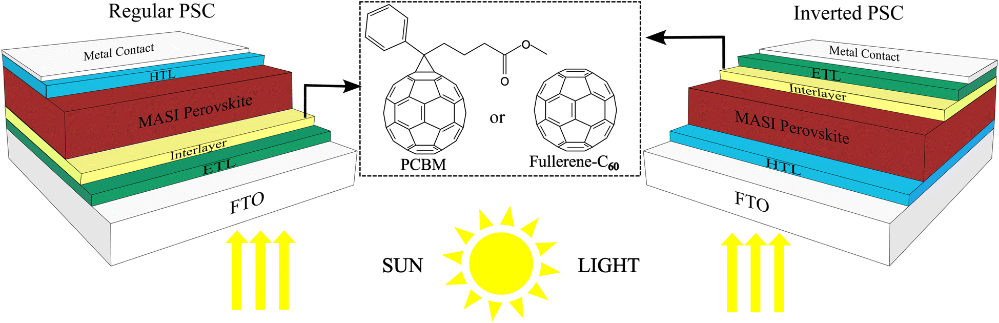 | ||
| Fig. 1 Interface engineering using fullerene-C60 and PCBM as interlayers between ETL and perovskite. | ||
2 Materials and methods
Hao et al.12 used composition engineering to optimize regular lead-free PSCs, thus achieving a PCE of 5.23% in their device using MASI perovskite (Spiro-MeOTAD/MASI/TiO2/FTO). Here, we use this solar cell as a means of validation and reference to simulate regular PSCs. We perform modifications, such as the inclusion of interlayers and changes in the ETL/HTL, in order to optimize the PSC. The solar cell developed by Hao et al.12 has also been used as a reference model in other simulation studies using SCAPS-1D.38,39For simulations of inverted PSCs, we use the work of Wang et al.58 as a reference, where an iPSC with the configuration PEDOT:PSS/MASI/PCBM/BCP was fabricated using the method of ion exchange and insertion reactions for layer deposition with a time of 60 minutes, achieving a PCE of 7.78%. The control iPSC using the one-step deposition method in this study achieved an efficiency of only 1.62%, even using the same HLT/ETL and SnF2 as an additive. This PCE was similar to those achieved by the iPSC using the new method with a time of 20 minutes (1.39%). Our simulation used as a validation method did not consider the method of ion exchange/insertion reactions for layer deposition and achieved an efficiency close to the control device of 1.18%. All the output parameters obtained with our simulation are very close to the device using the new method with 20 minutes time described in Wang et al.58 as shown in Table 1.
The thicknesses used to simulate the PSCs were 350 nm to MASI perovskite in regular and inverted configurations, and 200 nm to both HTLs (PEDOT:PSS and Spiro-MeOTAD), based on information from Hao et al.12 and Wang et al.58 The thickness used for the ETLs was 30 nm to TiO2 and 50 nm to PCBM. Finally, the value of Nt used in the simulations is 4.5 × 1017 cm−3.
The output parameters obtained in our simulations and those described in the reference articles of Hao et al.12 and Wang et al.58 are presented in Table 1. The output parameters from simulated PSCs in both configurations are close to the experimental values.
The values of input parameters used in our work, summarized in Tables 2–4 were taken from reference studies.38,39,46 The parameters referring to the HTLs PEDOT:PSS, Spiro-MeOTAD, and the ETL TiO2 are presented in Table S1 in ESI (ESI).†
| HTL | Perovskite | ETL | ETLs/Interlayers | |||
|---|---|---|---|---|---|---|
| Parameters/Materials | FTO39 | CuI55,59–61 | MASI12,38 | ZnO46,60 | C60 (ref. 46, 62 and 63) | PCBM46 |
| Thickness (nm) | 500 | Variable | Variable | 30 | Variable | Variable |
| Eg (eV) | 3.50 | 2.98 | 1.30 | 3.20 | 1.70 | 2.00 |
| χ (eV) | 4.00 | 2.10 | 4.17 | 4.26 | 3.90 | 3.90 |
| εr | 9.00 | 6.50 | 8.20 | 9.00 | 4.20 | 4.00 |
| Nc (cm−3) | 2.20 × 10¹⁸ | 2.80 × 10¹⁹ | 1.0 × 10¹⁸ | 2.00 × 10¹⁸ | 8.00 × 10¹⁹ | 1.00 × 10²¹ |
| Nv (cm−3) | 1.80 × 10¹⁹ | 1.00 × 10¹⁹ | 1.0 × 10¹⁸ | 1.80 × 10¹⁹ | 8.00 × 10¹⁹ | 2.00 × 10²⁰ |
| μe (cm2 V−1 s−1) | 20 | 100 | 1.6 | 100.00 | 0.08 | 0.02 |
| μh (cm2 V−1 s−1) | 10 | 2.00 | 1.6 | 5.00 | 3.5 × 10⁻³ | 0.02 |
| NA (cm−3) | — | 1.00 × 10¹⁸ | 3.2 × 10¹⁶ | — | — | — |
| ND (cm−3) | 2.00 × 10¹⁹ | — | — | 1.50 × 10¹⁷ | 2.60 × 10¹⁷ | 1.00 × 10²⁰ |
| Nt (cm−3) | 1.00 × 10¹⁵ | 1.00 × 10¹⁵ | Variable | 1.00 × 10¹⁵ | 1.00 × 10¹⁴ | 1.00 × 10¹⁴ |
| Parameters and units | ETL/MASI | HTL/MASI |
|---|---|---|
| Defect type | Acceptor | Acceptor |
| Capture cross section for electrons and holes (cm2) | 1.0 × 10⁻¹⁷ | 1.0 × 10⁻¹⁸ |
| 1.0 × 10⁻¹⁸ | 1.0 × 10⁻¹⁹ | |
| Energetic distribution | Single | Single |
| Energy level with respect to Ev (above Ev, eV) | Above the highest EV | Above the highest EV |
| Total density (cm−3) | 1.0 × 10⁹ | 1.0 × 10⁹ |
| Back metal contact | Ag | Cu | Au | Ni | Pt |
|---|---|---|---|---|---|
| Work function | 4.26 | 4.65 | 5.10 | 5.15 | 5.65 |
In our work, we simulated PSCs in regular and inverted configurations using fullerene-C60 and PCBM as interlayers, varying their thickness from 5 nm to 15 nm. First, the HTLs (Spiro-MeOTAD, PEDOT:PSS and CuI) and the ETLs (TiO2 and ZnO) are optimized. The MASI thickness varied between 150–800 nm, and the Nt of perovskite varied from 4.5 × 1013 cm−3 to 4.5 × 1017 cm−3.
3 Results and discussion
Here, we discuss the main results obtained by optimizing different parameters in both configurations of PSCs using version 3.3.08 of SCAPS-1D. All the simulations were realized using AM 1.5 G solar spectrum irradiance with 300 K of temperature.3.1 Optimization of HTL and ETL in n-i-p and p-i-n PSCs, using Nt = 4.5 × 1017 cm−3
Initially, the ETL and HTL were varied to analyze how the changes can influence the efficiency in solar cells of Hao et al.12 and Wang et al.58 in both configurations, considering the interfacial defects and using a high value of Nt (4.5 × 1017 cm−3) in the absorber material. Table S2† shows the PCE variation observed when Spiro-MeOTAD/CuI and PEDOT:PSS/CuI were employed as HTLs in regular and inverted PSCs, respectively, using different ETLs (TiO2 and ZnO).In both configuration simulations, the HTLs (Spiro-MeOTAD, PEDOT:PSS, and CuI) presented a thickness of 200 nm, and ETLs (TiO2 and ZnO) were 30 nm thick. The perovskite MASI thickness stays at 350 nm (Fig. 2). The transparent conductive oxide layer (TCO), in our case the fluorine-doped tin oxide (FTO), was omitted for the simulations of inverted PSCs since the HTL/FTO interface can be considered an ohmic contact.44
 | ||
| Fig. 2 Simulated PSCs in SCAPS-1D: regular n-i-p and inverted p-i-n. | ||
The organic HTL PEDOT:PSS presents difficulties in its application in solar cells, especially related to its low conductivity and defects in film morphology deposition, which leads to high charge recombination and consequently low values of FF and PCE.66 As related in other studies, despite Spiro-MeOTAD being one of the most used HTLs in planar PSCs, its use also finds difficulties related to this HTL environmental stability and during the solar cell fabrication process as well. In addition to it, Spiro-MeOTAD synthesis is expensive and this HTL is also commonly used with additives that interfere in the PSCs stability, despite increasing its conductivity.46
Inorganic HTLs such as CuI, Cu2O, and CuSCN have low cost and high stability, which makes them good candidates for replacement of organic HTLs.57 In particular, CuI has a large bandgap with an energy level close to perovskite and higher hole mobility of 0.5 to 2 cm2 V−1 s−1.67 However, these HTLs need low thickness to win the high device series resistance, which causes a challenge in regular PSC construction. Because of that, iPSCs are considered an excellent solution to overcome this problem.54
The simulated PSCs using CuI demonstrate superior performance in both regular and inverted configurations in all simulations compared to those using organic HTLs Spiro-MeOTAD and PEDOT:PSS with ZnO as the ETL, which is attributed to the higher hole mobility of CuI compared to organic HTLs. Considering the previously mentioned advantages of the inorganic HTL over the organic HTLs, we use CuI as HTL in the remaining simulations for both configurations. The next topic will discuss the optimization of CuI thickness.
A higher PCE is observed when zinc oxide replaced titanium dioxide in regular PCS in all simulations (Table S2†). While TiO2 boasts a good electron transfer capacity, its utilization requires high processing temperatures.68,69 Additionally, the Ti–O–Sn bond can contribute to increased charge recombination, as discussed earlier in this work.7 ZnO is a good alternative to TiO2 due to its similar band energy alignment and the fact that it does not require high-temperature processing.70
Table 5 shows the output parameters of n-i-p and p-i-n PSCs simulated in SCAPS-1D, varying the ETLs and using CuI/Spiro-MeOTAD as HTLs for regular PSCs and CuI/PEDOT:PSS as HTLs for inverted PSCs.
| Simulated PSCs | HTL/ETL | Voc (V) | Jsc (mA cm−2) | FF (%) | PCE (%) |
|---|---|---|---|---|---|
| a Simulations based on reference PSCs configurations. Regular PSC ref.: Spiro/TiO2, PCE = 5.23%;12 iPSC ref.: PEDOT:PSS/PCBM, PCE = 1.39%.58 | |||||
| n-i-pa | Spiro/TiO2 | 0.68 | 17.87 | 49.99 | 6.12 |
| n-i-p | CuI/TiO2 | 0.68 | 12.23 | 52.40 | 6.54 |
| n-i-p | CuI/ZnO | 0.68 | 18.70 | 53.82 | 6.89 |
| p-i-na | PEDOT/PCBM | 0.55 | 5.84 | 37.15 | 1.18 |
| p-i-n | CuI/TiO2 | 0.66 | 4.15 | 38.87 | 1.06 |
| p-i-n | CuI/ZnO | 0.62 | 4.83 | 45.04 | 1.35 |
The simulated device CuI/MASI/ZnO showed better results than the device using TiO2 in both configurations (6.89% and 1.35% for regular and inverted PSCs, respectively) due to the greater electron mobility of ZnO compared to TiO2.56
Jayan and Sebastian46 studied the effect of different HTLs and ETLs on the efficiency of regular MASI PSCs using SCAPS-1D software. The study achieved a PCE of 18.18% using CuI and ZnO as HTL/ETL. However, the authors used an ideal Nt of 2.5 × 1013 cm−3 and did not perform the study for iPSCs. The influence of different values of Nt will be discussed in the last topic of this work.
Several simulation studies have already evaluated the relationship between the PSC efficiency and the defect density values (Nt), both in the light-absorbing layer and at the device interfaces, varying it between 1013 and 1019 cm−3.39,71–74 It is observed that the lower the defect density in the absorber material, the higher its charge diffusion length (L), and this reduces charge recombination and increases the device efficiency.
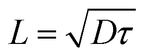
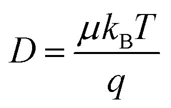
The charge diffusion length of the device is given by the square root of the product obtained between the diffusion coefficient (D) and the carrier lifetime (τ), which is the average time required for a carrier to recombine, given in cm, as shown in the eqn (1) and D is given by the eqn (2) in cm2 s−1.
 | (1) |
 | (2) |
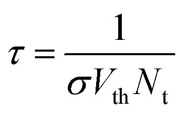
The carrier lifetime τ is given in the eqn (3).
 | (3) |
As shown by the formulas above, the defect density of the light-absorbing material is related to the value of the charge diffusion length of the device. Despite defect density values between 1013 cm−3 and 1015 cm−3 being ideal for achieving better output parameters in PSCs, studies about defect density in experimental cells have shown that values between 1016 cm−3 and 1017 cm−3 are commonly found in these devices.75,76 Here, we perform simulations using an Nt closer to those found in experimental solar cells.
3.2 Influence of MASI/CuI thickness and the different back contact metals on n-i-p and p-i-n PSCs
Due to the results presented in the last topic, all simulations are realized using CuI as HTL and ZnO as ETL. The ZnO thickness was 30 nm in all simulations, and the influence of HTL and MASI thickness will be evaluated.The thickness of CuI was varied from 200 nm to 30 nm, keeping the MASI thickness at 350 nm for both regular and inverted PCSs. There were no changes in the efficiencies of both configurations with varying thicknesses of the inorganic HTL. In the work of Wang et al. (2017),77 the authors fabricated an iPSC using CuI as the HTL with thicknesses of 20, 40, and 60 nm and found the optimal output parameters at a thickness of 40 nm. Based on this finding, we adopted a thickness of 40 nm for the HTL in our study.
Subsequently, we evaluated the MASI thickness influence in solar cell's PCE, varying the thickness from 150 nm to 800 nm in regular and inverted PSCs with an Nt at 4.5 × 1017 cm−3 and using the configuration CuI(40 nm)/MASI/ZnO(30 nm).
In both configurations, the decrease in the perovskite thickness reduces the light absorption rate, negatively impacting the device efficiency. However, very high thicknesses can increase the recombination of charges in the material.78 Devices with thicker perovskite exhibit significant charge extraction losses, and charge recombination occurs due to the comparatively slow speed of charge transport between the carrier layers compared to the light absorption rate.79
In a planar PSC, for optimal results, the charge diffusion value should be greater than the perovskite thickness.80,81 Table 6 shows the L and τ values to different Nt values, calculated from the described equations discussed in Subsection 3.1.
| Nt (cm−3) | L (nm) | τ (s) |
|---|---|---|
| 4.5 × 10¹³ | 676.50 | 1.11 × 10⁻⁷ |
| 4.5 × 10¹⁴ | 213.93 | 1.11 × 10⁻⁸ |
| 4.5 × 10¹⁵ | 67.65 | 1.11 × 10⁻⁹ |
| 4.5 × 10¹⁶ | 21.40 | 1.11 × 10⁻¹⁰ |
| 4.5 × 10¹⁷ | 6.76 | 1.11 × 10⁻¹¹ |
It is related in many studies involving simulated iPSCs that the PCE increases with perovskite thickness. However, these studies use a low Nt value.44,52,81 Fig. 3 shows the device efficiency variation as a function of perovskite thickness, using different Nt values ranging from 4.5 × 10¹³ to 4.5 × 1017 cm−3 for both regular and inverted PSCs.
 | ||
| Fig. 3 Contour graphs of the PCE values varying the MASI thickness and defect density of the absorber layer of regular (a) and inverted (b) PSCs. | ||
It is possible to observe in Fig. 4 and in Table S3 in ESI† the variation of the output parameters (Voc, Jsc, FF and PCE) as the MASI thickness increases.
 | ||
| Fig. 4 PCE, FF, Jsc and Voc of n-i-p (a) and p-i-n (b) PSCs, varying the MASI thickness, using ZnO and CuI as ETL/HTL (30 nm) and Nt of MASI in 4.5 × 1017 cm−3. | ||
When low values of Nt were used (1013 cm−3 and 1014 cm−3), the device's PCE increased with the perovskite thickness in both configurations. Regular PSCs maintained the pattern of increasing efficiency as the thickness increased, regardless of the defect density (Nt), as shown in Fig. 3. The thickness of n-i-p PSCs was optimized to 400 nm. As discussed by Lin et al.82 when the perovskite thickness decreases in regular PSCs, there is an increase in the hysteresis effect, leading to lower PCE values with very thin absorber layers.
On the other hand, unlike regular PSCs, the efficiency of iPSCs decreases as the thickness of the MASI perovskite increases when high values of Nt are employed (Fig. 3b). Considering the perovskite thickness between 150 to 800 nm, the highest PCE in iPSC was 3.72% using MASI with 150 nm thick. This behavior is attributed to non-radiative recombination linked to defects within the perovskite film.42 Fig. 5 shows that the charge recombination increased as the MASI thickness increased in iPSCs. As depicted in eqn (4), Shockley–Read–Hall recombination is directly associated with the carrier lifetime (τ) which, in turn, correlates with defect density (Nt).
 | (4) |
 | ||
| Fig. 5 PCE values and recombination rate peak based on MASI thickness variation in inverted PSC. | ||
Sun et al.83 achieved an efficiency of 7.40% in an experimental iPSC using MAPI with approximately 50 nm thick. The relationship between the perovskite thickness and exciton diffusion was analyzed using the Internal quantum efficiency (IQE) measurements to understand the PCE value observed in the device, concluding that the relationship between the two observed parameters was ideal. The authors emphasized that the value of L was close to the MAPI thickness. In our simulations using a high value of Nt (4.5 × 1017 cm−3), the perovskite thickness of p-i-n PSC was optimized to 150 nm.
The output parameters of the PSCs were evaluated in both configurations by varying the metals used as back contacts. The work function values of these metals are summarized in Table 4. Fig. S1† shows that in contrast to regular PSCs, inverted PSCs present higher PCE when metals with lower work functions are used.
Yue et al.84 built an iPSC using MAPI and measured its performance with metal cathodes with different work function values. They observed that metals with low work functions, such as Ca, Mg, Al, and Ag, resulted in superior device performance. The authors concluded that employing metals with high work functions, such as Au, caused a misalignment of energy levels within the light-absorbing layer towards the cathode, creating an upward band bend that hindered effective electron transport and consequently reduced solar cell efficiency. Similarly, Gong et al.85 conducted simulation work using MAPI perovskite to investigate the impact of metal cathodes on iPSCs, and they also concluded that metals like Au and Pt could generate an energy barrier towards the cathode.
Fig. 6 illustrates the band diagrams of iPSCs with CuI/MASI/ZnO configuration simulated in our study with different metal contacts. Similar to lead perovskites, it is possible to observe the upward curve of the energy levels from the tin perovskite towards the back contact metal as the work function of metals increases. Based on these results, the back contact metals selected for the remaining simulations are Au and Ag for regular and inverted PSCs, respectively.
 | ||
| Fig. 6 Band diagrams of lead-free iPSCs using metal contacts with different work function values. | ||
3.3 Fullerene-C60 and PCBM as interlayers in n-i-p and p-i-n MASI PSCs
In all simulations, fullerene-C60 and its derivative PCBM were utilized as interlayers between the ETL and the perovskite layer to enhance device performance in both regular and inverted configurations. The PSCs are simulated using an Nt of 4.5 × 1017 cm−3 and CuI and ZnO as HTL/ETL, respectively. The interlayer thickness varied from 5 to 15 nm, with the best results observed when the PCBM thickness was 15 nm due to the passivation effect reaching more trap states at the interface between the ETL and the perovskite layer as the interlayer thickness increased,86 Table 7.| Defect density Nt (cm−3) | PSC n-i-p | Interlayer thickness (nm) | PCE (%) | PSC p-i-n | Interlayer thickness (nm) | PCE (%) |
|---|---|---|---|---|---|---|
| 4.5 × 10¹⁷ | CuI/MASI/ZnO/FTO | — | 6.90 | CuI/MASI/ZnO | — | 3.72 |
| CuI/MASI/C60/ZnO/FTO | 5 | 5.68 | CuI/MASI/C60/ZnO | 5 | 3.33 | |
| CuI/MASI/C60/ZnO/FTO | 10 | 5.76 | CuI/MASI/C60/ZnO | 10 | 3.41 | |
| CuI/MASI/C60/ZnO/FTO | 15 | 6.10 | CuI/MASI/C60/ZnO | 15 | 3.66 | |
| CuI/MASI/PCBM/ZnO/FTO | 5 | 8.06 | CuI/MASI/PCBM/ZnO | 5 | 5.22 | |
| CuI/MASI/PCBM/ZnO/FTO | 10 | 8.09 | CuI/MASI/PCBM/ZnO | 10 | 5.24 | |
| CuI/MASI/PCBM/ZnO/FTO | 15 | 8.11 | CuI/MASI/PCBM/ZnO | 15 | 5.26 | |
| 4.5 × 10¹⁶ | CuI/MASI/ZnO | — | 11.85 | CuI/MASI/ZnO | — | 8.22 |
| CuI/MASI/PCBM/ZnO | 15 | 13.38 | CuI/MASI/PCBM/ZnO | 15 | 10.00 | |
| CuI/MASI/C60/ZnO | 15 | 11.05 | CuI/MASI/C60/ZnO | 15 | 8.15 |
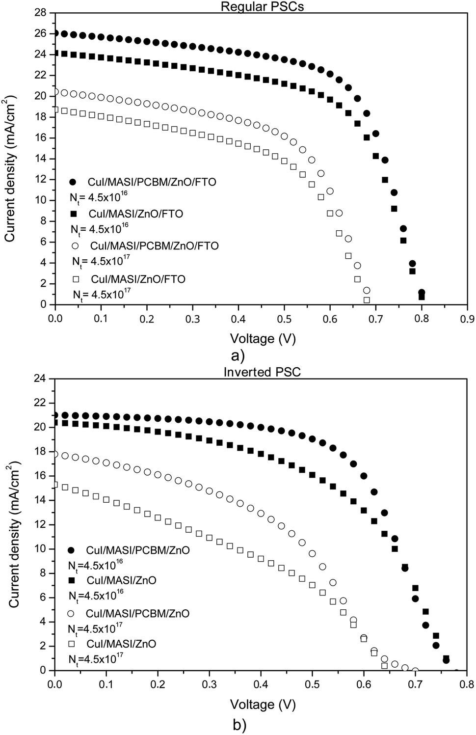
The simulations show that the PCE values for devices with interlayers are higher when PCBM is used instead of fullerene-C60 in both configurations, as observed in the quantum efficiency (QE) graph in Fig. 7, which represents the ratio between the number of charges generated in the solar device to the number of incident photons, and in JV curves, Fig. 8. This fact can be attributed to the energy difference between the LUMO orbitals of the interlayer and the perovskite, as shown in Fig. 9 for regular PSCs and in Fig. S2† for inverted PSCs. Using the fullerene derivative PCBM as an interlayer with a 15 nm thickness, a n-i-p PSC exhibited a device efficiency increase of 1.21% compared to the PSC without an interlayer, reaching 8.11%. For the p-i-n PSC, an efficiency increase of 1.54% was obtained, reaching 5.26%, Table 7 and Fig. 8. Using fullerene derivatives in smaller quantities as interlayers or additives can assist in optimizing lead-free PSCs by passivating possible defects in the crystal lattice formed during the deposition step.28
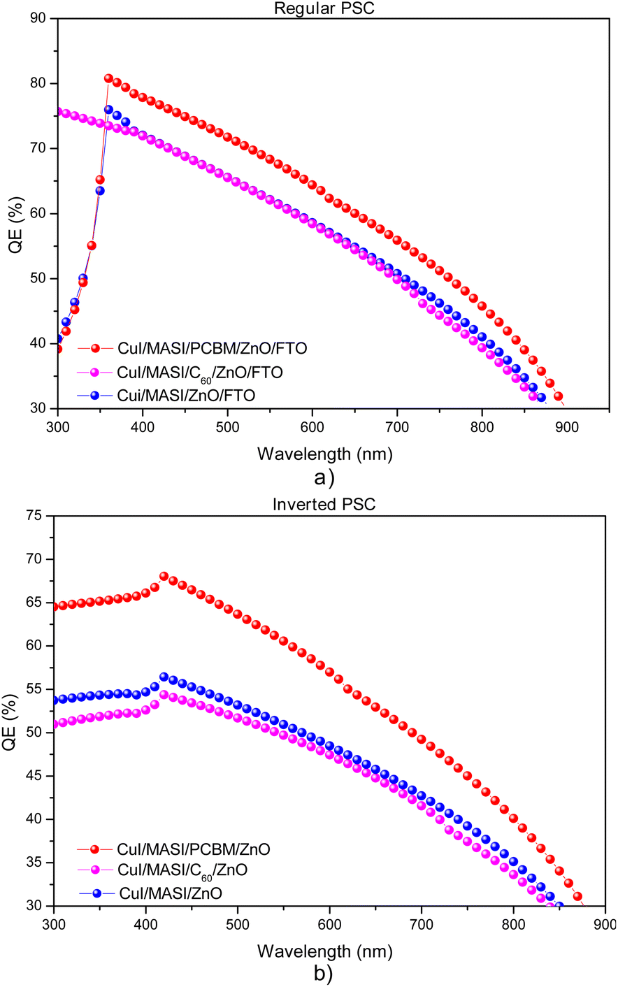 | ||
| Fig. 7 Quantum efficiency graph of PSCs in (a) regular and (b) inverted configurations. | ||
 | ||
| Fig. 8 JV curves of PSCs using fullerene-C60 and PCBM (15 nm thickness) as interlayers between ZnO and MASI in both regular (a) and inverted (b) configurations. | ||
 | ||
| Fig. 9 Energy diagram of simulated regular PSCs. (a) CuI/MASI/ZnO, (b) CuI/MASI/C60/ZnO, (c) CuI/MASI/PCBM/ZnO, using Nt = 4.5 × 1017 cm−3 and MASI thickness at 400 nm. | ||
When fullerene-C60 was used as an interlayer in regular PSCs, all results were worse compared to the devices simulated without interlayers (Table 7), in both configurations. As shown in Fig. 9C to the regular PSCs and Fig. S2 (ESI)† to the iPSCs, the LUMO energy level of PCBM is close to the MASI perovskite, which helps in electron extraction. In simulated PSC using fullerene-C60 as an interlayer a slight energy barrier to electron transfer occurs between the MASI layer and the ETL (Fig. 9 and S2†), which hampers electron mobility. The electron energy barrier at the interface perovskite/ETL is crucial as it determines how efficiently electrons can be transferred between the layers. Electron losses due to recombination occur during the transport of photogenerated charges between the various layers of the PSC. A high energy barrier can lead to significant recombination losses, reducing the current generated by the solar cell and decreasing its efficiency.87
3.4 Influence of defect density (Nt) in regular and inverted PSCs using fullerene-C60 and PCBM as interlayers
Here, we will evaluate how changing the defect density in perovskite layer can influence the PCE. Initially, the Nt value of perovskite MASI is changed between 4.5 × 1017 cm−3 and 4.5 × 1013 cm−3 in n-i-p and p-i-n PSCs, maintaining the MASI thickness in 400 nm and 150 nm for regular and inverted PSCs, respectively, and using PCBM as interlayer. As shown in Fig. 10, the JV curve increases when the Nt value decreases for both configurations. | ||
| Fig. 10 Comparison of JV curves using PCBM as an interlayer at different values of defect density (Nt) of PSCs in (a) regular and (b) inverted configurations. | ||
Although the PCE increases with the decrease in the Nt value, we discreetly reduced the Nt value from 4.5 × 10¹⁷ to 4.5 × 1016 cm−3, maintaining an Nt value close to that found in experimental solar cells.75 The MASI thickness was already optimized for different values of Nt, as discussed in Section 3.2. When PCBM is used as an interlayer, PCE significantly increased, rising from 8.11% to 13.38% for regular PSCs and from 5.26% to 10.00% for inverted PSCs, as shown in Table 7, considering 150 nm to iPSC and 700 nm to regular PSC in this simulations.
Fig. 11 compares JV curves of the devices using an Nt of 4.5 × 1017 cm−3 and 4.5 × 1016 cm−3 and PCBM as an interlayer between ZnO and MASI. As observed in both configurations, using a PCBM interlayer helps increase the PCE when high values of Nt are used due to its surface defect passivation effect. A lower defect density in the absorber material increases the PSC's efficiency, even without using interlayers between the ETL and the perovskite. However, using PCBM as an interlayer significantly increases the PCE value (Table 7).
 | ||
| Fig. 11 JV curve of simulated PSCs in n-i-p (a) and p-i-n (b) configurations with and without interlayers using different values of Nt and PCBM as an interlayer (15 nm). Empty symbols represent PSCs using Nt of 4.5 × 1017 cm−3, and filled symbols represent simulated PSCs with an Nt of 4.5 × 1016 cm−3. | ||
For the simulations considering an ideal Nt of 4.5 × 1013 cm−3, the MASI thickness of regular and inverted PSCs was 800 and 750 nm, respectively, as optimized in Subsection 3.2. Interlayers did not positively affect the PSC performance in both configurations. Lower defect densities in the perovskite material result in fewer trap states and reduced charge recombination between layers, enhancing the PCE. In this context, the interlayers play a less significant role, as the device does not require passivation of the absorber layer. The simulations using PCBM as an interlayer achieved nearly the same results as simulations without interlayers, as shown in Table S4.† However, in the simulations using fullerene-C60 as an interlayer, the PCE significantly decreased, similar to what occurred with higher Nt values.
4 Conclusion
The objective of our work was to understand how the use of fullerene-C60 and its derivative PCBM could affect lead-free PSCs using MASI in both regular and inverted configurations. We observed from simulation results that the inorganic HTL, CuI, could be considered a good alternative to organic HTLs in lead-free PSCs for achieving improved output parameters for solar cells in both configurations. The HTL CuI and MASI perovskite thicknesses were optimized and a PCE of 6.90% and 3.72% was achieved for the regular and inverted PSCs, respectively.Using a fullerene derivative as an interlayer could positively influence the PCE of MASI PSCs when the inorganic ETL, ZnO, is used in both configurations due to better electron extraction and defect passivation. Using PCBM as an interlayer, with 15 nm thick, in simulations with a high value of defect density (Nt = 4.5 × 1017 cm−3) in the absorber layer caused an increase in the device's efficiency, from 6.90% to 8.11%. In iPSCs with CuI/MASI/PCBM/ZnO configuration, also occurs an increase of 1.54% as compared to MASI PSC without an interlayer, and the device achieved a PCE of 5.26%.
However, when fullerene-C60 was used as an interlayer, device performance had no positive impact, and a decrease in PCE of regular and inverted PSCs was observed compared to devices without an interlayer. This occurs due to the difference in energy level between the interlayer and MASI perovskite layer, which causes recombination losses. The optoelectronic properties of fullerene-C60 derivatives need to be such that they do not negatively impact device performance while also serving their purpose of passivating interfacial recombination sites.
Decreasing the defect density to 4.5 × 1016 cm−3 in the light absorbing material for devices with CuI/MASI/PCBM/ZnO configuration in n-i-p and p-i-n PSCs, better results were found and the PCE reached 13.38% for regular PSC and 10.00% for the iPSC. Considering an ideal Nt of 4.5 × 1013 cm−3, it was observed in both simulated PSCs that the use of PCBM as interlayer did not significantly interfere the efficiency of the solar device. As the defect density in the perovskite layer is small, the PCBM passivation effect was not that significant.
Finally, our SCAPS-1D simulations revealed that employing fullerene derivatives such as PCBM in thin layers as interlayers can positively impact lead-free PSCs using MASI, especially in the inverted configuration. We hope our findings will contribute to ongoing research efforts to enhance the efficiency and stability of MASI PSCs.
Conflicts of interest
There are no conflicts to declare.Acknowledgements
We would like to thank Professor Marc Burgelman and the Electronics and Information Systems (ELIS), University of Gent of Belgium, for providing us with free access to the SCAPS 1D simulation tool. We also want to thank CAPES and FAPEMIG for supporting this research project.References
- V. H. D. Araujo, G. M. Fernandes, G. C. Costa, L. J. dos Santos and J. C. Tristão, Rev. Virtual Quim., 2022, 14, 427–442 CrossRef CAS.
- K. P. Goetz, A. D. Taylor, Y. J. Hofstetter and Y. Vaynzof, ACS Appl. Mater. Interfaces, 2020, 13, 1–17 CrossRef PubMed.
- A. Abate, Joule, 2017, 1, 659–664 CrossRef CAS.
- Z. Zhao, F. Gu, Y. Li, W. Sun, S. Ye, H. Rao, Z. Liu, Z. Bian and C. Huang, Advanced Science, 2017, 4, 1700204 CrossRef PubMed.
- M. K. Hossain, G. I. Toki, A. Kuddus, M. Rubel, M. Hossain, H. Bencherif, M. F. Rahman, M. R. Islam and M. Mushtaq, Sci. Rep., 2023, 13, 2521 CrossRef CAS PubMed.
- R. M. I. Bandara, S. M. Silva, C. C. Underwood, K. I. Jayawardena, R. A. Sporea and S. R. P. Silva, Energy Environ. Mater., 2022, 5, 370–400 CrossRef CAS.
- K. Hamada, R. Tanaka, M. A. Kamarudin, Q. Shen, S. Iikubo, T. Minemoto, K. Yoshino, T. Toyoda, T. Ma and D.-W. Kang, et al., ACS Appl. Mater. Interfaces, 2020, 12, 17776–17782 CrossRef CAS PubMed.
- M. H. Kumar, S. Dharani, W. L. Leong, P. P. Boix, R. R. Prabhakar, T. Baikie, C. Shi, H. Ding, R. Ramesh and M. Asta, et al., Adv. Mater., 2014, 26, 7122–7127 CrossRef CAS PubMed.
- W. Liao, D. Zhao, Y. Yu, C. R. Grice, C. Wang, A. J. Cimaroli, P. Schulz, W. Meng, K. Zhu and R.-G. Xiong, et al., Adv. Mater., 2016, 28, 9333–9340 CrossRef CAS PubMed.
- E. L. Lim, A. Hagfeldt and D. Bi, Energy Environ. Sci., 2021, 14, 3256–3300 RSC.
- M. A. Kamarudin, D. Hirotani, Z. Wang, K. Hamada, K. Nishimura, Q. Shen, T. Toyoda, S. Iikubo, T. Minemoto and K. Yoshino, et al., J. Phys. Chem. Lett., 2019, 10, 5277–5283 CrossRef CAS PubMed.
- F. Hao, C. C. Stoumpos, D. H. Cao, R. P. Chang and M. G. Kanatzidis, Nat. Photonics, 2014, 8, 489–494 CrossRef CAS.
- K. Nishimura, M. A. Kamarudin, D. Hirotani, K. Hamada, Q. Shen, S. Iikubo, T. Minemoto, K. Yoshino and S. Hayase, Nano Energy, 2020, 74, 104858 CrossRef CAS.
- Z. Zhu, X. Jiang, D. Yu, N. Yu, Z. Ning and Q. Mi, ACS Energy Lett., 2022, 7, 2079–2083 CrossRef CAS.
- A. Mahapatra, D. Prochowicz, M. M. Tavakoli, S. Trivedi, P. Kumar and P. Yadav, J. Mater. Chem. A, 2020, 8, 27–54 RSC.
- W. Zeng, X. Liu, X. Guo, Q. Niu, J. Yi, R. Xia and Y. Min, Molecules, 2017, 22, 520 CrossRef PubMed.
- N. K. Tailor, M. Abdi-Jalebi, V. Gupta, H. Hu, M. I. Dar, G. Li and S. Satapathi, J. Mater. Chem. A, 2020, 8, 21356–21386 RSC.
- H. Hu, S. Moghadamzadeh, R. Azmi, Y. Li, M. Kaiser, J. C. Fischer, Q. Jin, J. Maibach, I. M. Hossain and U. W. Paetzold, et al., Adv. Funct. Mater., 2022, 32, 2107650 CrossRef CAS.
- T. Gatti, E. Menna, M. Meneghetti, M. Maggini, A. Petrozza and F. Lamberti, Nano Energy, 2017, 41, 84–100 CrossRef CAS.
- A. Rajagopal, P.-W. Liang, C.-C. Chueh, Z. Yang and A. K.-Y. Jen, ACS Energy Lett., 2017, 2, 2531–2539 CrossRef CAS.
- G. Kapil, T. S. Ripolles, K. Hamada, Y. Ogomi, T. Bessho, T. Kinoshita, J. Chantana, K. Yoshino, Q. Shen and T. Toyoda, et al., Nano Lett., 2018, 18, 3600–3607 CrossRef CAS PubMed.
- H. Li, Y. Xue, B. Zheng, J. Tian, H. Wang, C. Gao and X. Liu, RSC Adv., 2017, 7, 30422–30427 RSC.
- L. Jia, M. Chen and S. Yang, Mater. Chem. Front., 2020, 4, 2256–2282 RSC.
- B. Wang, J. Yang, L. Lu, W. Xiao, H. Wu, S. Xiong, J. Tang, C. Duan and Q. Bao, Adv. Mater. Interfaces, 2020, 7, 1901964 CrossRef CAS.
- J. Xie, X. Yu, X. Sun, J. Huang, Y. Zhang, M. Lei, K. Huang, D. Xu, Z. Tang and C. Cui, et al., Nano Energy, 2016, 28, 330–337 CrossRef CAS.
- X. Guo, B. Zhang, Z. Lin, J. Ma, J. Su, W. Zhu, C. Zhang, J. Zhang, J. Chang and Y. Hao, Org. Electron., 2018, 62, 459–467 CrossRef CAS.
- H. Wang, F. Cai, M. Zhang, P. Wang, J. Yao, R. S. Gurney, F. Li, D. Liu and T. Wang, J. Mater. Chem. A, 2018, 6, 21368–21378 RSC.
- T. Zheng, L. Fan, H. Zhou, Y. Zhao, B. Jin and R. Peng, ACS Appl. Mater. Interfaces, 2020, 12, 24747–24755 CrossRef CAS PubMed.
- B. Li, J. Zhen, Y. Wan, X. Lei, L. Jia, X. Wu, H. Zeng, M. Chen, G.-W. Wang and S. Yang, J. Mater. Chem. A, 2020, 8, 3872–3881 RSC.
- C. Tian, K. Lin, J. Lu, W. Feng, P. Song, L. Xie and Z. Wei, Small Methods, 2020, 4, 1900476 CrossRef CAS.
- Y.-C. Niu, L.-F. Yang, M. Aldamasy, M. Li, W.-J. Lan, Q. Xu, Y. Liu, S.-L. Feng and Y.-G. Yang, Rare Met., 2021, 40, 2747–2762 CrossRef CAS.
- C.-H. Hsieh, Y.-J. Cheng, P.-J. Li, C.-H. Chen, M. Dubosc, R.-M. Liang and C.-S. Hsu, J. Am. Chem. Soc., 2010, 132, 4887–4893 CrossRef CAS PubMed.
- S.-K. Huang, Y.-C. Wang, W.-C. Ke, Y.-T. Kao, N.-Z. She, J.-X. Li, C.-W. Luo, A. Yabushita, D.-Y. Wang and Y. J. Chang, et al., J. Mater. Chem. A, 2020, 8, 23607–23616 RSC.
- M. Shahiduzzaman, K. Yamamoto, Y. Furumoto, T. Kuwabara, K. Takahashi and T. Taima, Chem. Lett., 2015, 44, 1735–1737 CrossRef CAS.
- D. Li, W. Kong, H. Zhang, D. Wang, W. Li, C. Liu, H. Chen, W. Song, F. Gao and A. Amini, et al., ACS Appl. Mater. Interfaces, 2020, 12, 20103–20109 CrossRef CAS PubMed.
- J. Seo, S. Park, Y. C. Kim, N. J. Jeon, J. H. Noh, S. C. Yoon and S. I. Seok, Energy Environ. Sci., 2014, 7, 2642–2646 RSC.
- Y.-F. Chen, Z.-M. Luo, C.-H. Chiang and C.-G. Wu, ACS Appl. Mater. Interfaces, 2022, 14, 46603–46614 CrossRef CAS PubMed.
- D. Jalalian, A. Ghadimi and A. Kiani, Eur. Phys. J.: Appl. Phys., 2019, 87, 10101 CrossRef CAS.
- H.-J. Du, W.-C. Wang and J.-Z. Zhu, Chin. Phys. B, 2016, 25, 108802 CrossRef.
- A. Niemegeers and M. Burgelman, Conference Record of the Twenty Fifth IEEE Photovoltaic Specialists Conference-1996, 1996, pp. 901–904 Search PubMed.
- M. S. Rahman, S. Miah, M. S. W. Marma and T. Sabrina, 2019 International Conference on Electrical, Computer and Communication Engineering (ECCE), 2019, pp. 1–6 Search PubMed.
- S. Z. Haider, H. Anwar, S. Manzoor, A. G. Ismail and M. Wang, Curr. Appl. Phys., 2020, 20, 1080–1089 CrossRef.
- N. Lakhdar and A. Hima, Opt. Mater., 2020, 99, 109517 CrossRef CAS.
- A. Wang, X. Gan and J. Yu, Opt. Mater., 2021, 112, 110751 CrossRef CAS.
- L. Lin, P. Li, L. Jiang, Z. Kang, Q. Yan, H. Xiong, S. Lien, P. Zhang and Y. Qiu, Sol. Energy, 2021, 215, 328–334 CrossRef CAS.
- K. D. Jayan and V. Sebastian, Sol. Energy, 2021, 217, 40–48 CrossRef.
- M. S. Salem, A. Shaker, A. Zekry, M. Abouelatta, A. Alanazi, M. T. Alshammari and C. Gontand, Energies, 2021, 14, 5741 CrossRef CAS.
- M. Kumar, A. Raj, A. Kumar and A. Anshul, Opt. Mater., 2020, 108, 110213 CrossRef CAS.
- I. Chabri, Y. Benhouria, A. Oubelkacem, A. Kaiba, I. Essaoudi and A. Ainane, J. Electron. Mater., 2023, 52, 2722–2736 CrossRef CAS.
- A. K. Al-Mousoi, M. K. Mohammed, R. Pandey, J. Madan, D. Dastan, G. Ravi and P. Sakthivel, et al., RSC Adv., 2022, 12, 32365–32373 RSC.
- M. K. Hossain, M. S. Uddin, G. I. Toki, M. K. Mohammed, R. Pandey, J. Madan, M. F. Rahman, M. R. Islam, S. Bhattarai and H. Bencherif, et al., RSC Adv., 2023, 13, 23514–23537 RSC.
- M. Shamna, K. Nithya and K. Sudheer, Mater. Today: Proc., 2020, 33, 1246–1251 CAS.
- T. Lenka, A. Soibam, K. Dey, T. Maung and F. Lin, CSI Transactions on ICT, 2020, 8, 111–116 CrossRef.
- N. Ghalambaz, J. Ganji and P. Shabani, Opt. Quantum Electron., 2021, 53, 315 CrossRef CAS.
- S. Karthick, J. Bouclé and S. Velumani, Sol. Energy, 2021, 218, 157–168 CrossRef CAS.
- A. Mohandes, M. Moradi and M. Kanani, Opt. Quantum Electron., 2023, 55, 533 CrossRef CAS.
- S. Z. Haider, H. Anwar, Y. Jamil and M. Shahid, J. Phys. Chem. Solids, 2020, 136, 109147 CrossRef CAS.
- P. Wang, F. Li, K.-J. Jiang, Y. Zhang, H. Fan, Y. Zhang, Y. Miao, J.-H. Huang, C. Gao, X. Zhou, F. Wang, L.-M. Yang, C. Zhan and Y. Song, Advanced Science, 2020, 7, 1903047 CrossRef CAS PubMed.
- B. N. Ezealigo, A. C. Nwanya, A. Simo, R. U. Osuji, R. Bucher, M. Maaza and F. I. Ezema, Arabian J. Chem., 2019, 12, 5380–5391 CrossRef CAS.
- C. R. Kishor, T. Sreelakshmy, A. Das and P. Aneesh, Phys. B, 2022, 639, 414020 CrossRef CAS.
- G. Pindolia, S. M. Shinde and P. K. Jha, Sol. Energy, 2022, 236, 802–821 CrossRef CAS.
- E. O. Kweitsu, S. K. Armoo, K. Kan-Dapaah, E. K. K. Abavare, D. Dodoo-Arhin and A. Yaya, Molecules, 2020, 26, 120 CrossRef PubMed.
- T. Rabenau, A. Simon, R. Kremer and E. Sohmen, Z. Phys. B: Condens. Matter., 1993, 90, 69–72 CrossRef CAS.
- Y. Raoui, H. Ez-Zahraouy, N. Tahiri, O. El Bounagui, S. Ahmad and S. Kazim, Sol. Energy, 2019, 193, 948–955 CrossRef CAS.
- F. Behrouznejad, S. Shahbazi, N. Taghavinia, H.-P. Wu and E. W.-G. Diau, J. Mater. Chem. A, 2016, 4, 13488–13498 RSC.
- Y. Xia and S. Dai, J. Mater. Sci.: Mater. Electron., 2021, 32, 12746–12757 CrossRef CAS.
- P.-K. Kung, M.-H. Li, P.-Y. Lin, Y.-H. Chiang, C.-R. Chan, T.-F. Guo and P. Chen, Adv. Mater. Interfaces, 2018, 5, 1800882 CrossRef.
- E. Raphael, M. N. Silva, R. Szostak, M. A. Schiavon and A. F. Nogueira, Quim. Nova, 2018, 41, 61–74 CAS.
- R. Wang, M. Mujahid, Y. Duan, Z.-K. Wang, J. Xue and Y. Yang, Adv. Funct. Mater., 2019, 29, 1808843 CrossRef CAS.
- C. Otalora, M. Botero and G. Ordonez, J. Mater. Sci., 2021, 56, 15538–15571 CrossRef CAS.
- A. S. Chouhan, N. P. Jasti and S. Avasthi, Mater. Lett., 2018, 221, 150–153 CrossRef CAS.
- M. Jamal, S. Shahahmadi, M. A. A. Wadi, P. Chelvanathan, N. Asim, H. Misran, M. Hossain, N. Amin, K. Sopian and M. Akhtaruzzaman, Optik, 2019, 182, 1204–1210 CrossRef CAS.
- C. Pathak and S. K. Pandey, et al., IEEE Trans. Electron Devices, 2020, 67, 2837–2843 Search PubMed.
- S. Abdelaziz, A. Zekry, A. Shaker and M. Abouelatta, Opt. Mater., 2020, 101, 109738 CrossRef CAS.
- N. K. Noel, S. D. Stranks, A. Abate, C. Wehrenfennig, S. Guarnera, A.-A. Haghighirad, A. Sadhanala, G. E. Eperon, S. K. Pathak and M. B. Johnston, et al., Energy Environ. Sci., 2014, 7, 3061–3068 RSC.
- M. Jiang, F. Lan, Q. Tao, G. Li, B. Zhao, J. Wu and D. Gao, Appl. Phys. Lett., 2016, 108, 1–4 Search PubMed.
- H. Wang, Z. Yu, X. Jiang, J. Li, B. Cai, X. Yang and L. Sun, Energy Technol., 2017, 5, 1836–1843 CrossRef CAS.
- E. Danladi, D. S. Dogo, S. U. Michael, F. O. Uloko and A. A. O. Salawu, East Eur. J. Phys., 2021, 5–17 Search PubMed.
- T. Du, W. Xu, S. Xu, S. R. Ratnasingham, C.-T. Lin, J. Kim, J. Briscoe, M. A. McLachlan and J. R. Durrant, J. Mater. Chem. C, 2020, 8, 12648–12655 RSC.
- H. Dixit, D. Punetha and S. K. Pandey, Optik, 2019, 179, 969–976 CrossRef CAS.
- A. Thankappan and S. Thomas, Perovskite Photovoltaics: Basic to Advanced Concepts and Implementation, Academic Press, 2018 Search PubMed.
- X. Lin, D. Cui, X. Luo, C. Zhang, Q. Han, Y. Wang and L. Han, Energy Environ. Sci., 2020, 13, 3823–3847 RSC.
- S. Sun, T. Salim, N. Mathews, M. Duchamp, C. Boothroyd, G. Xing, T. C. Sum and Y. M. Lam, Energy Environ. Sci., 2014, 7, 399–407 RSC.
- S. Yue, S. Lu, K. Ren, K. Liu, M. Azam, D. Cao, Z. Wang, Y. Lei, S. Qu and Z. Wang, Small, 2017, 13, 1700007 CrossRef PubMed.
- J. Gong and S. Krishnan, Energy Sustainability, 2019, 1–6 Search PubMed.
- Y.-C. Shih, L. Wang, H.-C. Hsieh and K.-F. Lin, ACS Appl. Mater. Interfaces, 2018, 10, 11722–11731 CrossRef CAS PubMed.
- Y. Da, Y. Xuan and Q. Li, Sol. Energy Mater. Sol. Cells, 2018, 174, 206–213 CrossRef CAS.
Footnote |
| † Electronic supplementary information (ESI) available. See DOI: https://doi.org/10.1039/d4ra00634h |
| This journal is © The Royal Society of Chemistry 2024 |