
 Open Access Article
 This Open Access Article is licensed under a Creative Commons Attribution-Non Commercial 3.0 Unported Licence
Electronic and magnetic properties of transition-metal-doped monolayer B2S2 within GGA + U framework
Wei Chen *a,
Qi Chenb,
Jianming Zhangc,
Lin Zhoua,
Wenxiao Tanga,
Zhiyou Wanga,
Jiwei Denga and
Shifeng Wangd
*a,
Qi Chenb,
Jianming Zhangc,
Lin Zhoua,
Wenxiao Tanga,
Zhiyou Wanga,
Jiwei Denga and
Shifeng Wangd
aSchool of Electronic Information and Electrical Engineering, Changsha University, Changsha, 410022, China. E-mail: po_ze_xi@126.com
bZhongxiang No. 2 Middle School, Jingmen, 431900, China
cInstitute of Physics and Electronic Information, Yunnan Normal University, Kunming 650500, China
dCollege of Information Engineering, Hunan Industry Polytechnic, 410000, China
First published on 22nd January 2024
Abstract
Considering the significant role of magnetism induction in two-dimensional (2D) semiconductor materials, we systematically investigate the effects of various dopants from the 3d and 4d transition metal (TM) series, including Ti, V, Mn, Fe, Co, Ni, Cu, Zn, Zr, Nb, Mo, Ru, Rh, Pd, Ag and Cd, on the electronic and magnetic properties of monolayer B2S2 through first-principles calculations. The calculated formation energies indicate that substitutional doping at the B site with various TM atoms could be achieved under S-rich growth conditions. What matters is that with the exception of systems doped with Cu, Tc, and Ag elements, which exhibit non-magnetic semiconductor properties, all other doped systems demonstrate magnetism. Specifically, the Cr-, Ni- and Pd-doped monolayers are magnetic half-metals, while the rest are magnetic semiconductors. We have also performed calculations of magnetic couplings between two TM atoms with an impurity concentration of 3.12%, revealing the prevalence of weak magnetic coupling in the majority of the magnetic systems examined. Moreover, the monolayers doped with Cr, Zr and Pd atoms exhibit ferromagnetic ground states. These findings strongly support the high potential for inducing magnetism in the B2S2 monolayer through B-site doping.
1. Introduction
The presence of magnetic behavior in two-dimensional (2D) layered materials has sparked significant interest due to its implications for fundamental research and potential applications in the fields of spintronics and memory devices.1–6 Particularly, atomically thin nanosheets Gr2Ge2Te6 (ref. 1) and CrI3 (ref. 2) have exhibited intrinsic ferromagnetism, generating significant excitement in the scientific community. Building upon this progress, researchers have achieved room-temperature ferromagnetic (FM) order in few-atomic-layer Fe3GeTe2 through the implementation of ionic gate modulation,3 pushing the boundaries of spintronics research. Furthermore, researchers have successfully measured the electric field-induced antiferromagnetic–ferromagnetic (AFM–FM) phase transition4 and the corresponding tunneling magnetoresistance5 in CrI3, demonstrating groundbreaking findings that pave the way for the future development of 2D spintronic devices.In addition to 2D layered materials displaying intrinsic magnetism, extensive efforts have been made by researchers to introduce magnetic properties into nonmagnetic counterparts, driven by the recognition that a majority of discovered 2D materials lack inherent magnetism. Various methodologies have been explored, encompassing doping,7–9 defect and strain engineering,10,11 nanoribbon formation,12,13 and atom adsorption.14–21 Among these strategies, substitutional doping has emerged as a widely employed and effective technique, substantiated by theoretical predictions and experimental validations. First-principles calculations have demonstrated that doping transition-metal (TM) atoms, alkaline-earth atoms, or nonmetal atoms can induce magnetism into nonmagnetic systems.8,9,22–25 Experimentally, researchers have successfully achieved ferromagnetism in doped phosphorene, graphene, and transition-metal dichalcogenides (TMD) MX2 (M = Mo, Sn; X = S, Se, Te) utilizing diverse doping techniques such as chemical vapor deposition (CVD) and low-energy ion implantation.26–31 These accomplishments usher in exciting prospects for customizing magnetism in a wide range of 2D materials.
Recently, the successful synthesis of B2S2,32 a lighter new member in the TMD-like 2D material family, has garnered people's attention. Tunable bandgap, excellent lithium-ion battery performance and broadband photoluminescence response, render 2D B2S2 highly promising for electronic devices, energy conversion and storage, catalysis, and sensors. Computational calculations reveal that monolayer B2S2 is a non-magnetic semiconductor with bandgaps of 3.00 and 4.06 eV, as determined by GGA and HSE06 methods, respectively.32 Although 2D-B2S2 is currently considered a non-magnetic semiconductor, the potential introduction of magnetism into it could further expand its applications in spintronics.
Here, we present an investigation into the magnetic properties of monolayer B2S2 doped with TM atoms from the 3d- and 4d-series utilizing first-principles calculations. The outcomes of our investigation reveal the effective implementation of magnetism in the TM doped systems, showcasing the potential for their application in spintronics based on B2S2 monolayer.
2. Computational methods
The calculations were conducted employing the density functional theory (DFT)33,34 framework within the generalized gradient approximation (GGA)35 known as Perdew–Burke–Ernzerhof (PBE)36 implemented in the advanced Vienna ab initio simulation package (VASP). The projector-augmented wave (PAW)35 method was employed for accurate description of the ion–electron interaction. As the TM-d orbitals may have strong correlation effects,37 the GGA + U method was carried out for calculation, and the on-site Coulomb interaction parameters U11,38–43 for TM atoms are listed in Table 1. To simulate the effects of doping, a (4 × 4 × 1) supercell containing 64 atoms was constructed. Additionally, a smaller (3 × 3 × 1) supercell with 36 and a larger (5 × 5 × 1) supercell with 100 atoms was tested, confirming the robustness of the main findings. All crystal structures were relaxed until the residual forces acting on individual atoms reached a convergence criterion of less than 0.01 eV Å−1. The self-consistency criteria for electronic structures were set at a high level of 10−6 eV. An energy cutoff of 550 eV was chosen to ensure accurate plane-wave basis expansion. Structural optimizations employed a (3 × 3 × 1) gamma-centered k-grid, while the calculation of the density of states (DOS) utilized a (6 × 6 × 1) k-grid. Furthermore, to avoid interlayer interactions, a vacuum region of 20 Å was included in the direction perpendicular to the layers. We have further introduced the van der Waals correction (D3)21,44,45 to describe the effect of van der Waals interactions, but practical testing revealed that this correction did not qualitatively affect the main conclusions in our paper.| 3d-TM | U | Eg (eV) | Mtot (μB) | MTM (μB) | MB (μB) | MS (μB) | 4d-TM | U | Eg (eV) | Mtot (μB) | MTM (μB) | MB (μB) | MS (μB) |
|---|---|---|---|---|---|---|---|---|---|---|---|---|---|
| Ti | 4.4 | 1.61 | 1.00 | 1.20 | −0.10 | −0.05 | Zr | 5.0 | 1.32 | 1.00 | 1.09 | −0.07 | −0.02 |
| V | 2.7 | 1.80 | 2.00 | 2.15 | −0.12 | −0.10 | Nb | 2.1 | 1.62 | 2.00 | 1.74 | −0.05 | −0.05 |
| Cr | 3.5 | — | 3.00 | 3.47 | −0.21 | −0.23 | Mo | 2.4 | 0.93 | 1.00 | 0.92 | −0.03 | −0.03 |
| Mn | 4.0 | 1.24 | 4.00 | 4.15 | −0.24 | −0.01 | Tc | 2.7 | 2.15 | 0.00 | 0 | 0 | 0 |
| Fe | 4.6 | 1.27 | 3.00 | 3.14 | −0.17 | 0.02 | Ru | 3.0 | 0.74 | 1.00 | 0.63 | −0.01 | 0.10 |
| Co | 5.0 | 1.27 | 2.00 | 1.97 | −0.10 | 0.04 | Rh | 3.3 | 0.82 | 2.00 | 1.12 | −0.03 | 0.31 |
| Ni | 5.1 | — | 1.00 | 0.60 | −0.03 | 0.20 | Pd | 3.6 | — | 1.00 | 0.32 | −0.01 | 0.31 |
| Cu | 4.0 | 1.07 | 0.00 | 0 | 0 | 0 | Ag | 5.0 | 0.76 | 0.00 | 0 | 0 | 0 |
| Zn | 7.5 | 0.58 | 1.00 | 0.13 | 0.21 | 0.10 | Cd | 2.1 | 0.56 | 1.00 | 0.12 | 0.21 | 0.08 |
3. Results and discussion
The TMD-like 2D B2S2 belongs to the hexagonal system with P3m1 space group,32 which has a similar structure as TMDs such as MoS2, with Mo atoms replaced by vertically aligned B2 atom pairs, forming an S–B–B–S tetralayer sheet, as shown in Fig. 1(a). In our calculations, the optimized lattice constant a0, the average B–S bond length dB–S, the B–B bond length dB–B, and the distance between two S layers dS–S are 1.95, 1.70, and 3.40 Å, respectively. The S–B–S bond angle θ is 102.90°. These data is very consistent with previous reports.32 Next, Fig. 1(b) shows the top and side views of atomic structure for the doped B2S2 monolayer. A (4 × 4 × 1) supercell is employed to simulate the TM doped system, in which the substitution of one B atom by one TM atom yielded a doping concentration of 3.12%. Geometric structure optimization results reveal that all doped systems maintain the original structural type of the pristine B2S2 monolayer, albeit exhibiting slight lattice distortion.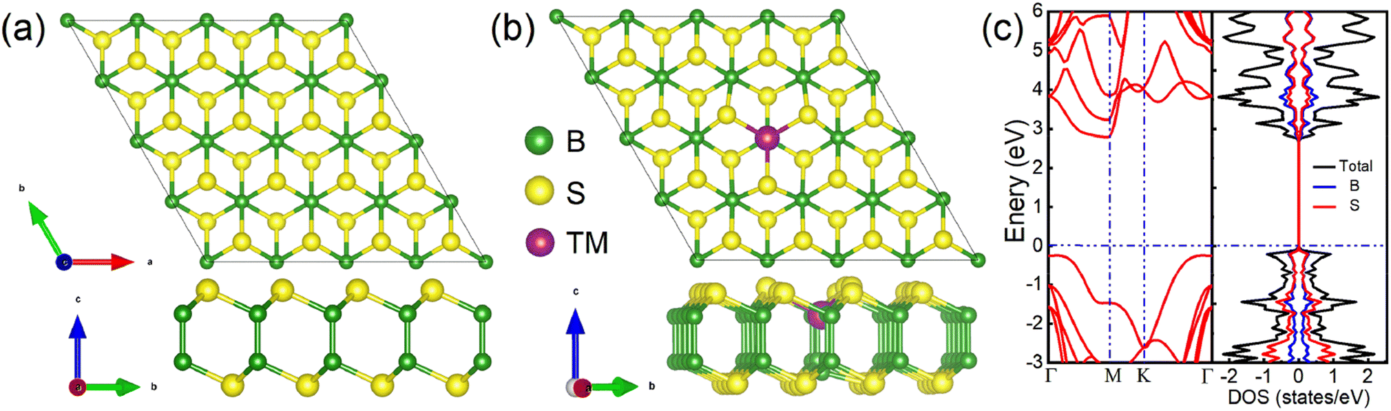 | ||
| Fig. 1 Schematic structures. Top and side views of atomic structure for (a) the pure (4 × 4 × 1) B2S2 monolayer and (b) the doped (4 × 4 × 1) B2S2 monolayer. The green, yellow, and purple spheres represent boron, sulfur, and transition metal atoms, respectively. (c) The band structure and partial density of states (PDOS) for the pure B2S2 monolayer per unit cell. The horizontal dashed vertical line indicates the Fermi level, which is set to the zero of the energy. | ||
To reveal the influence of impurity atoms on the electronic properties of the pure system, we firstly present the band structure and partial density of states (PDOS) of monolayer B2S2 per unit cell along the high-symmetry direction in the first Brillouin zone, as shown in Fig. 1(c). It is evident that monolayer B2S2 show semiconductor nature with no branch across the Fermi level. It possesses an indirect band gad of 3.01 eV with the conduction band minimum (CBM) locating at the M point and the valence band maximum (VBM) lying in the region along the Γ → K direction. The completely symmetric DOSs for the spin-down and spin-up states illustrates the nonmagnetic nature of the system. The PDOSs for B and S atoms manifests a strong covalent bond hybridization due to their similar energy distributions. Our calculations are in agreement with the previous results,32 demonstrating that the calculation method is reasonable and reliable.
Next, we assess the energetic stability of the doped crystal structures. The binding energy (Eb) was calculated using the formula: Eb = Ed − (Ev + ETM).9,20,25 In this equation, Ed represents the energy of the (4 × 4 × 1) B2S2 monolayer doped with one dopant atom, Ev is the total energy of the (4 × 4 × 1) doped layer with a B vacancy, and ETM corresponds to the energy of an isolated dopant atom. The larger negative value of Eb means the more thermodynamic stability of the doped systems. Fig. 2(a) shows the calculated binding energies for various TM doped B2S2 monolayer. It illustrates that doping with 3d-TM atoms results in negative binding energies for all doped systems, whereas a portion of the 4d-TM doped systems (i.e. Nb-, Mo, Pd, Ag, and Cd-doped systems) exhibit positive binding energies, thereby implying that 3d-TM doping is energetically more favourable to B2S2 than 4d-TM doping. It should be pointed out that the positive binding energy indicates that the reaction is endothermic and requires an external supply of energy to proceed, does not mean doping is not feasible experimentally. In addition, formation energies (Efrom) of the doped systems are computed for both B-rich and S-rich conditions, with detail calculations provided in the referenced literature,8,9,24 i.e., Efrom = (Edoped − Epure) + (μB − μTM). Where Edoped and Epure are the energies of the (4 × 4 × 1) TM-doped and pure monolayers, respectively. μB and μTM respectively represent the energy of isolated B and impurity TM atoms. In the B-rich limit, the chemical potential of B atom (μB) can be represented by the energy of a B atom in its bulk, while in the S-rich limit, is defined by the energy difference between one formula unit (B2S2) of stoichiometric 2D-B2S2 monolayer and the chemical potential of S atom (μS) determined from its bulk, i.e., μB = (B2S2 − 2μS)/2. Our results, as illustrated in Fig. 2(b) and (c), show that all TM-doped models have negative formation energies under the S-rich condition, whereas under the B-rich condition, they exhibit positive formation energies. This observation implies that achieving doping is significantly easier under S-rich conditions and confirms the energetic favorability of the doped systems.
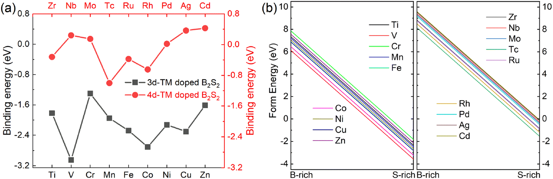 | ||
| Fig. 2 (a) The binding energies and (b) formation energies under B-rich and S-rich conditions of the different 3d- and 4d-TM doped B2S2 monolayers. | ||
To disclose the electronic characteristic and magnetic behavior induced by the TM dopants in the B2S2 monolayers, we have plotted the band structures of different doped systems in Fig. 3. The ground state and the magnetic moments are given in Table 1. With the exception of systems doped with Cu, Tc, and Ag elements, which exhibits non-magnetic semiconductor properties, all other TM-doped systems demonstrate magnetism. The Mn-doped system has the largest magnetic moment of 4μB. Among the magnetic systems, the Cr-, Ni-, and Pd-doped systems behave as half-metals with magnetic moments of 3, 1 and 1μB, respectively, while the rest are magnetic semiconductors. The half-metallic systems are the source of fully spin-polarized electrons and promising for high efficiency spintronic devices. Moreover, since the dopants introduce impurity bands, the band gaps of the doped systems with semiconductor characteristics are smaller than that of the pristine B2S2 monolayer, as shown in Table 1. We can predict that the use of the HSE functional will further increase the band gap of semiconductors, potentially leading to a transition from a semimetal to a semiconductor state. However, this will not affect our conclusions regarding magnetism. Anyway, the calculated results clearly shows that tunable magnetic and electronic properties can be achieved in B2S2 by doping with TM atoms.
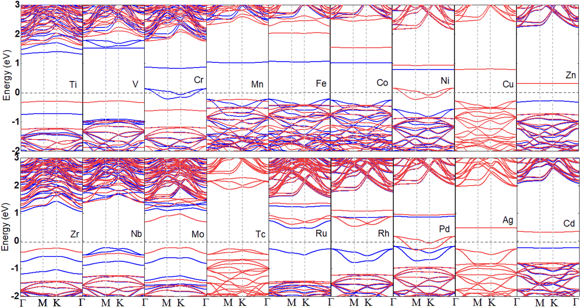 | ||
| Fig. 3 The calculated band structures of a 3d- and 4d-TM doped B2S2 monolayers with 3.12% doping. The spin-up and spin-down states are represented by the blue and red lines, respectively. The zero of the energy is set to the Fermi level, shown by the grey lines. | ||
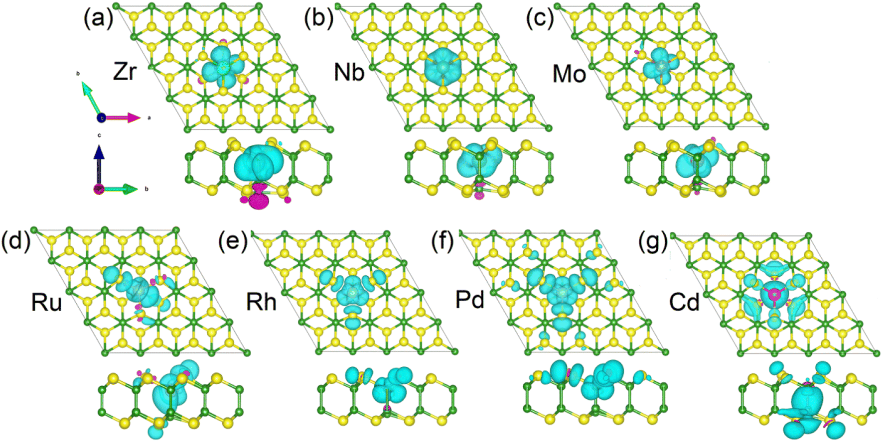
Due to the different variations in magnetic moments between 3d and 4d TM-doped systems, we now proceed to separately discuss the magnetic origins of them. To visualize the detailed distribution of magnetic moments in 3d TM-doped monolayers, we present the spin densities of the magnetic systems in Fig. 4. This graphical representation allows for a comprehensive understanding of the spatial distribution and magnitude of magnetic moments within the materials. It is evident from the figures (Fig. 4(a)–(f)) that the magnetic moments of the Ti-, V-, Cr-, Mn-, Fe- and Co-doped systems predominantly originate from the 3d TM dopants. In the case of the Ni-doped monolayer, part of the contribution also comes from the three nearest neighboring (NN) S atoms (see Fig. 4(g)). Conversely, for the Zn-doped monolayer, the magnetic moment is primarily contributed by the NN and next neighbor S atoms and the NN B atom (see Fig. 4(h)). Table 1 presents the total magnetic moments (Mtot), the moments of 3d-TM dopant atom (MTM), the three NN S atoms (MS) and one NN B atom (MB), respectively.
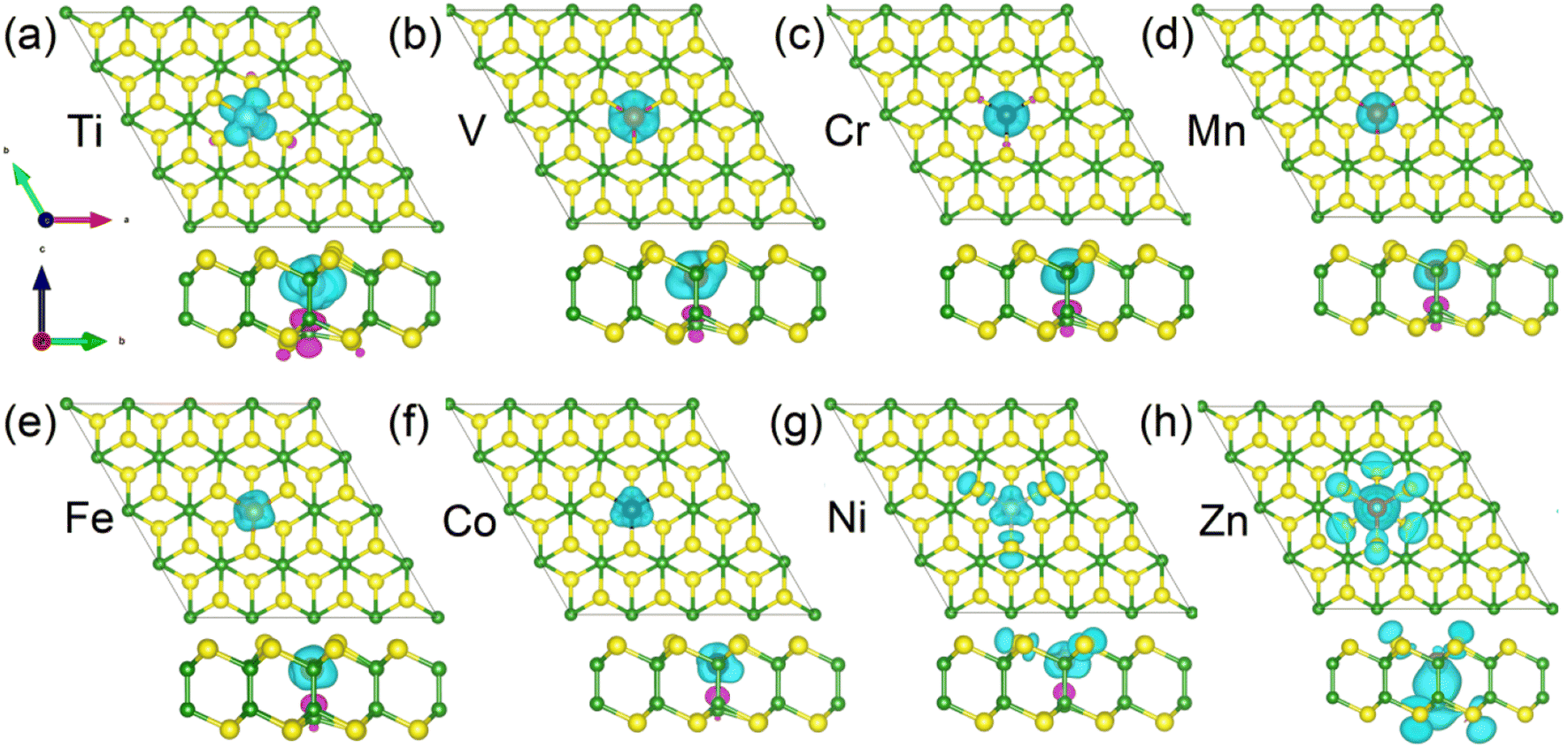 | ||
| Fig. 4 (a–h) The spin density distribution of 3d-TM doped B2S2 monolayers with 3.12% doping from both the top and the side view. Isovalue is 0.02 eV Å−3. The spin-up and spin-down densities are represented by the sky blue and purple isosurfaces, respectively. | ||
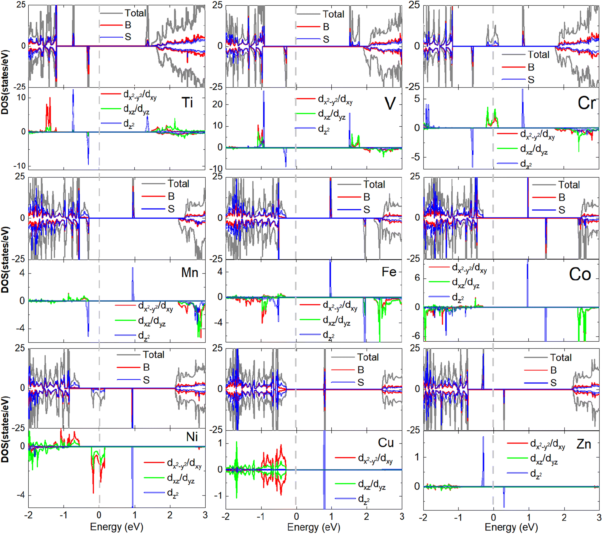
To understand the orbital dependency of the magnetism of 3d-TM doped B2S2 monolayers, we plot the total density of states (DOS) and corresponding partial density of states (PDOS) projected onto the 3d-TM dopants and their neighboring S and B atoms, as shown in Fig. 5. In nonmagnetic system, the Cu-doped monolayer, the electronic structures exhibit spin symmetry between the spin-up and spin-down channels. In contrast, magnetic systems (including the Ti-, V-, Cr-, Mn-, Fe-, Co-, and Zn-doped monolayers) display spin-splitting between these channels, thereby demonstrating their inherent magnetic properties. When considering the origin of half-metallicity in the Cr- and Ni-doped monolayers, it is observed that both the TM-3d states and S-p states intersect the Fermi energy level, leading to the emergence of half-metallic behavior. Moreover, the TM-3d orbitals, the S-p and B-p orbitals overlap near the Fermi energy level, indicating hybridization between the dopant atoms and their neighboring S and B atoms.
 | ||
| Fig. 5 The total and projected density of states of 3d-TM doped B2S2 monolayers with 3.12% doping. The Fermi energy is shifted to zero energy as indicated by the vertical dashed black line. | ||
The PODS of TM-3d orbitals are further decomposed according to the crystal symmetry. As the optimized structures of TM-doped systems maintain the D3d symmetry, according to the ligand field theory, the TM-3d atomic orbitals under the action of crystal field are split into three sets: a single a1(dz2) state and two twofold degenerate e1(dx2−y2, dxy) and e2(dyz, dxz) states. The spin-splitting near the Fermi level primarily arises from the exchange splitting and crystal field splitting of the TM-3d states. Fig. 5 illustrates that exchange splitting is absent in the Cu-3d orbitals, whereas exchange splitting occurs in the 3d orbitals of the remaining 3d-TM atoms. It is well-known that isolated Ti, V, Cr, Mn, Fe, Co, Ni, Cu, Zn, and B atoms possess electronic configurations of 3d24s2, 3d34s2, 3d54s1, 3d54s2, 3d64s2, 3d74s2, 3d84s2, 3d104s1, 3d104s2 and s2p1, respectively. Therefore, for substitution of 2-valent B, all 3d-TM atoms will act as the n-type dopants. In agreement with the simple ionic model, the additional unpaired 3d-electrons introduced by the dopant atoms should occupy only the spin-up (or spin-down) defect states. Due to the fact that Ti, V, Cr, and Mn atoms have one, two, three, and four more electrons than B atoms, the magnetic moments of the Ti-, V-, Cr-, and Mn-doped systems should be 1, 2, 3, and 4μB, respectively. For Fe-, Co-, Ni- and Cu-doped monolayers, the a1(dz2) orbital is unoccupied (see Fig. 5). Then, the extra electrons present in the four types of dopant atoms (including Fe, Co, Ni and Cu) compared to the B atom will occupy the e1(dx2−y2, dxy) and e2(dyz, dxz) orbitals. Fe atom has five more electrons than B atom, one extra valence electron occupies the spin state opposite to the other four, resulting in the magnetic moment of the system being 3μB. The same reason is obtained for the systems doped with Co, Ni, and Cu. For example, the Cu-doped monolayer is nonmagnetic as half of the eight more electrons occupy the spin-up states and the remaining electrons occupy the spin-down states. The magnetic moment of the Zn-doped monolayer is 1μB because the p orbitals of the neighboring S and B atoms are occupied by one unpaired electron from Zn-3d orbitals caused by the hybridization between the three kind orbitals. In general, with the increase of the 3d-TM atomic number, the total moments (Mtot) of the doped systems show an overall increasing trend followed by a decreasing trend. Similar trends have also been observed in the study of doped monolayers of CrX3 (X = Br, I),46,47 MoS2,48 and phosphorene.49
The spin densities of the 4d TM-doped magnetic systems are present in Fig. 6. The magnetic moments of the Zr-, Nb-, and Mo-doped monlayers are mainly contributed by dopants (see Fig. 6(a)–(c)). For the systems doping with Ru and Rh, a small portion of the contribution also comes from the NN S atoms (see Fig. 6(d) and (e)). While for Ph-doped monolayers, the magnetic moments contributed by the NN S and Pd atom are roughly equal (see Fig. 6(d)–(f)). In the case of the Cd-doped system, the magnetic moment primarily originates from the NN and next neighbor S atoms and the NN B atom (see Fig. 4(g)). The specific contributions of NN S and B atoms, as well as impurity atoms, to the magnetic moment can be found in Table 1.
 | ||
| Fig. 6 (a–g) The calculated spin densities of 4d-TM doped B2S2 monolayers with 3.12% doping from both the top view and the side view. Isovalue is 0.02 eV Å−3. The spin-up and spin-down densities are represented by the sky blue and purple isosurfaces, respectively. | ||
Fig. 7 shows the total density of states (DOS) and corresponding partial density of states (PDOS) projected onto the 4d-TM dopants and their neighboring S and B atoms. It can be found that the Zr-doped monolayer has 1μB magnetic moment as e2 state is occupied by one excessive valence electron. In the monolayer doped with Nb, two excessive valence electrons occupies the e1 and e2 states, giving 2μB magnetic moment. For the Mo-doped monolayer, one more valence electron than the Nb ion occupies the spin-down e1 (e2) state, leading to a total magnetic moment of 1μB. In the Tc-doped monolayer, the net magnetic moment is zero due to the distribution of half of the four surplus valence electrons in the spin-up e1 and e2 states, while the remaining electrons occupy the spin-down e1 and e2 states. The magnetic moments of the Ru-, Rh-, and Pd-doped systems are determined to be 1, 2 and 1μB, respectively, as a result of three out of the five electrons in Ru atom, four out of the six electrons in Rh atom, and four out of the seven electrons in Pd atom occupying opposite spin e1 and e2 states to the remaining two, two, and three electrons, respectively. No exchange splitting occurs for the Ag-4d orbitals. The p spin-up orbitals of the neighboring B and S atoms are occupied by one unpaired electron from Cd-4d orbitals caused by the hybridization between the three kind orbitals, generating 1μB magnetic moments in the monolayer doped with Cd.
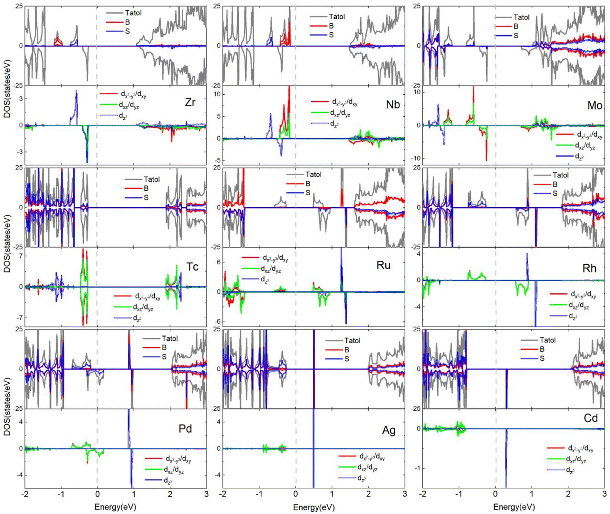 | ||
| Fig. 7 The total and projected density of states of 4d-TM doped B2S2 monolayers with 3.12% doping. The Fermi energy is shifted to zero energy as indicated by the vertical dashed black line. | ||
For 2D systems, the magnetic anisotropy energy plays an essential role for offsetting the thermal fluctuation to maintain the magnetic ordering.50 We further calculate magnetocrystalline anisotropy energies (MAE) of the TM-doped monolayers by employing the GGA + U + SOC approach. The cutoff energy and the corresponding energy criterion used for MAE calculations are improved to 600 eV and 10−8 eV, respectively. Using the force theorem,51,52 self-consistent calculations are performed to obtained the total energies for in-plane and out-of-plane magnetization directions, respectively, and MAE is evaluated by the difference between the total energies for the two magnetization directions, defined as MAE = E[100] − E[001], where E[100] and E[001] are the total energies when magnetization is in plane and normal to the plane, respectively. The negative MAE denotes the in-plane easy magnetization [100] axis and the positive one indicates their easily magnetized direction is the [001] axis. The summary of MAEs for the TM-doped magnetic systems are listed in Table 2. The results show that Cr-, Ni-, Nb- and Pd-doped monolayers are most likely to have long range magnetic order because of their large MAEs of 3.50, 16.08, −1.10 and 2.17 meV, respectively. It has been proposed that the MAE of Co-doped phosphorene and MoS2 (ref. 22) monolayer are 1.0 and −3.58 meV.22,26 Our current MAE results are largely consistent with these proposals, with the exception of Ni-doped system. In comparison, the MAE of Ni-doped system can be compared to that of Ir-doped g-C3N4 (ref. 53) and Re doped-antimonene,8 which are 12.4 and 18.33 meV, respectively. Hence, TM-doped B2S2 systems with the sizeable MAE are auspicious to be the candidates for their practical application in magnetic memory and storage devices.8,22
| 3d-TM | MAE (meV) | E↑↑ (meV) | E↑↓ (meV) | ΔE (meV) | 4d-TM | MAE (meV) | E↑↑ (meV) | E↑↓ (meV) | ΔE (meV) |
|---|---|---|---|---|---|---|---|---|---|
| Ti | 0.05 | −735.5779 | −735.5795 | 1.6 | Zr | 0.34 | −733.6547 | −733.6516 | −3.2 |
| V | −0.03 | −739.5357 | −739.5374 | 1.7 | Nb | −1.10 | −739.4466 | −739.4546 | 8.1 |
| Cr | 3.50 | −739.0099 | −739.0073 | −2.6 | Mo | 0.93 | −738.8166 | −738.8177 | 1.1 |
| Mn | −0.24 | −739.7030 | −739.7056 | 2.6 | Tc | — | — | — | — |
| Fe | 0.21 | −736.6786 | −736.6804 | 1.8 | Ru | 0.05 | −736.3168 | −736.3150 | 2.6 |
| Co | 0.27 | −734.6019 | −734.6036 | 1.6 | Rh | 0.50 | −733.3499 | −733.3237 | 26.7 |
| Ni | 16.08 | −731.8776 | −731.8814 | 3.8 | Pd | 2.17 | −728.8058 | −729.4866 | −62.8 |
| Cu | 0.00 | — | — | — | Ag | — | — | — | — |
| Zn | −0.01 | −727.8701 | −727.8708 | 0.7 | Cd | −0.01 | −723.9198 | −723.9188 | 1.0 |
To further investigate the magnetic ground state of the TM doped magnetic systems and the exchange coupling between the two magnetic atoms, we have expanded the (4 × 4 × 1) supercell to a larger (8 × 4 × 1) supercell comprising 128 atoms. FM and AFM coupling are calculated by specifying parallel and anti-parallel alignment of the moments produced by two same TM atoms in the supercell. The interatomic distances between the two TM dopants, which participate in the long-range coupling interaction, measure 12.18 Å. The energy difference between the FM and AFM states are listed in Table 2. Since groups Cu-, Tc- and Ag-doped monolayers display nonmagnetic character, we have not performed the calculations for these systems. It is evident that the magnetic coupling between the two substituted dopants in most TM-doped systems is significantly weak due to the minimal energy difference. This similarity is also observed in previous investigations when U correction is taken into account.8,48,54 The weak coupling interaction between two TM atoms maybe attributed to the localization correction of d-orbitals, which requires experiment to validate in future studies. In addition, the results show that the Cr-, Zr- and Pd-doped monolayers have the FM ground state, which are 2.6, 3.2 and 62.8 meV lower in energy than the AFM states, respectively, while for the rest of the magnetic doped systems, the ground state is AFM. Since the Curie temperature (TC) is the a key parameter for FM materials. Based on the mean-field theory and Ising model, TC is estimated by the equation:25,48,55 ΔE = E↑↑ − E↑↓ = −N(3/2)kBTC. Here E↑↓ and E↑↑ are the total energies of the AFM and FM states, respectively. kB is Boltzmann constant. N is the number of dopant atoms in the supercell. The calculated Curie temperatures of the Cr-, Zr- and Pd-doped monolayers are 10, 12 and 243 K, respectively. It's worth noting that the Curie temperatures of Ga1−xMnxAs layer,56 TM-doped MoS2 and CrX3 (X = Br, I) monolayers46–48 are approximately 100 K or below. So we demonstrate that Pd-doped B2S2 monolayer show robust ferromagnetism that surpasses the Ga1−xMnxAs, MoS2 and CrX3 (X = Br, I) layers. The notable characteristics of Pd-doped B2S2 system, including its half-metallic ferromagnetic properties, relatively high Curie temperature, and significant perpendicular magnetic anisotropy, position it as a promising candidate for spin electronics applications, such as advanced magnetic recording, magnetic storage, high-efficiency magnetic sensors, and spin-emitting diodes.
4. Conclusion
In summary, we study magnetic properties of monolayer B2S2 introduced by doping 3d- and 4d-TM atoms by means of first-principles calculations. The calculation show the binding energies of all 3d-TM doped B2S2 systems are negative, suggesting their thermodynamical stability, whereas a portion of the 4d-TM doped systems (i.e., Nb, Mo, Pd, Ag, and Cd-doped systems) exhibit positive binding energies. The formation energies indicate that the inclusion of TM dopants is more energetically favorable under S-rich conditions. More importantly, except for the monolayers doped with Cu, Tc and Ag atoms, which do not exhibit magnetic properties, all other TM-doped systems have been introduced with magnetism. Among these magnetic systems, the Cr-, Ni- and Pd-doped monolayers are magnetic half-metals, while the rest are magnetic semiconductors. Besides these, our analysis revealed a prevalent occurrence of weak magnetic coupling in the majority of the examined magnetic systems. The Cr-, Zr- and Pd-doped monolayers exhibit FM ground states. Our findings provide evidence that substitutional doping at the B site offers a highly promising strategy for inducing magnetism in monolayer B2S2 based low-dimensional spintronic devices.Conflicts of interest
The authors declare no competing financial interests.Acknowledgements
This work was supported by the Hunan Provincial Natural Science Foundation of China (2023JJ40074, 2023JJ60499, 2022JJ30635), Hunan Provincial Department of Education project (21B0757, 22A0599, 22B0821), Yunnan Province Natural Science Foundation (00900206020616034).References
- C. Gong, L. Li, Z. L. Li, H. W. Ji, A. Stern, Y. Xia, T. Cao, W. Bao, C. Z. Wang, Y. A. Wang, Z. Q. Qiu, R. J. Cava, S. G. Louie, J. Xia and X. Zhang, Nature, 2017, 546, 265 CrossRef CAS PubMed.
- B. Huang, G. Clark, E. Navarro-Moratalla, D. R. Klein, R. Cheng, K. L. Seyler, D. Zhong, E. Schmidgall, M. A. McGuire, D. H. Cobden, W. Yao, D. Xiao, P. Jarillo-Herrero and X. D. Xu, Nature, 2017, 546, 270 CrossRef CAS PubMed.
- Y. J. Deng, Y. J. Yu, Y. C. Song, J. Z. Zhang, N. Z. Wang, Z. Y. Sun, Y. F. Yi, Y. Z. Wu, S. W. Wu, J. Y. Zhu, J. Wang, X. H. Chen and Y. B. Zhang, Nature, 2018, 563, 94 CrossRef CAS PubMed.
- D. R. Klein, D. MacNeill, J. L. Lado, D. Soriano, E. Navarro-Moratalla, K. Watanabe, T. Taniguchi, S. Manni, P. Canfield, J. Fernández-Rossier and P. Jarillo-Herrero, Science, 2018, 360, 1218 CrossRef CAS PubMed.
- T. C. Song, X. H. Cai, M. W. Y. Tu, X. O. Zhang, B. V. Huang, N. P. Wilson, K. L. Seyler, L. Zhu, T. Taniguchi, K. Watanabe, M. A. McGuire, D. H. Cobden, D. Xiao, W. Yao and X. D. Xu, Science, 2018, 360, 1214 CrossRef CAS PubMed.
- W. Chen, J. M. Zhang, Y. Z. Nie, Q. L. Xia and G. H. Guo, J. Magn. Magn. Mater., 2020, 508, 166878 CrossRef CAS.
- L. Yang, H. Wu, W. F. Zhang, X. Lou, Z. J. Xie, X. Yu, Y. Liu and H. X. Chang, Adv. Electron. Mater., 2019, 5, 1900552 CrossRef CAS.
- M. Zhang, H. M. Guo, J. Lv and H. S. Wu, Appl. Surf. Sci., 2020, 508, 145197 CrossRef CAS.
- W. Chen, J. M. Zhang, X. G. Wang, Q. L. Xia, Y. Z. Nie and G. H. Guo, J. Magn. Magn. Mater., 2021, 518, 167433 CrossRef CAS.
- A. O'Neill, S. Rahman, Z. Zhang, P. Schoenherr, T. Yildirim, B. Gu, G. Su, Y. R. Lu and J. Seidel, ACS Nano, 2023, 17, 735–742 CrossRef PubMed.
- W. Chen, J. M. Zhang, Y. Z. Nie, Q. L. Xia and G. H. Guo, J. Phys. Chem. Solids, 2020, 143, 109489 CrossRef CAS.
- G. Z. Magda, X. Z. Jin, I. Hagymási, P. Vancsó, Z. Osváth, P. Nemes-Incze, C. Y. Hwang, L. P. Biró and L. Tapasztó, Nature, 2014, 514, 608 CrossRef CAS PubMed.
- L. Z. Kou, C. Tang, Y. Zhang, T. Heine, C. F. Chen and T. Frauenheim, J. Phys. Chem. Lett., 2012, 3, 2934–2941 CrossRef CAS PubMed.
- R. N. Somaiya, Y. Sonvane and S. K. Gupta, Comput. Mater. Sci., 2020, 173, 109414 CrossRef CAS.
- S. M. Aghaei, M. M. Monshi, I. Torres, S. M. J. Zeidi and I. Calizo, Appl. Surf. Sci., 2018, 427, 326–333 CrossRef.
- S. K. Gupta, D. Singh, K. Rajput and Y. A. Sonvane, RSC Adv., 2016, 6, 102264 RSC.
- J. Q. Zhang, C. Zhang, K. Ren, X. L. Lin and Z. Cui, Nanotechnology, 2022, 33, 345705 CrossRef PubMed.
- A. Bafekry, M. Faraji, M. M. Fadlallah, A. B. Khatibani, A. A. Ziabari, M. Ghergherehchi, S. Nedaei, S. F. Shayesteh and D. Gogova, Appl. Surf. Sci., 2021, 559, 149862 CrossRef CAS.
- K. Chen, W. Q. Tang, M. M. Fu, X. Li, C. M. Ke, Y. P. Wu, Z. M. Wu and J. Y. Kang, Nanoscale Res. Lett., 2021, 16, 104 CrossRef CAS PubMed.
- T. Hussain, D. Singh, S. K. Gupta, A. Karton, Y. Sonvane and R. Ahuja, Appl. Surf. Sci., 2019, 469, 775–780 CrossRef CAS.
- Y. Yong, W. Zhang, Q. Hou, R. Gao, X. Yuan, S. Hu and Y. Kuang, Appl. Surf. Sci., 2022, 606, 154806 CrossRef CAS.
- Y. Yue, C. Jiang, Y. Han, M. Wangc, J. Ren and Y. Wu, J. Magn. Magn. Mater., 2020, 496, 165929 CrossRef CAS.
- Y. X. Zhang and Q. Y. Hou, Appl. Surf. Sci., 2023, 637, 157831 CrossRef CAS.
- J. M. Zhang, H. L. Zheng, R. L. Han, X. B. Du and Y. Y. Yan, J. Alloys Compd., 2015, 647, 75–81 CrossRef CAS.
- M. Kar, R. Sarkar, S. Pal and P. Sarkar, J. Phys.: Condens. Matter, 2019, 31, 145502 CrossRef PubMed.
- L. Seixas, A. Carvalho and A. H. Castro Neto, Phys. Rev. B: Condens. Matter Mater. Phys., 2015, 91, 155138 CrossRef.
- M. Tripathi, A. Mittelberger, N. A. Pike, C. Mangler, J. C. Meyer, M. J. Verstraete, J. Kotakoski and T. Susi, Nano Lett., 2018, 18, 5319–5323 CrossRef CAS PubMed.
- K. H. Zhang, S. M. Feng, J. J. Wang, A. Azcatl, N. Lu, R. Addou, N. Wang, C. J. Zhou, J. Lerach, V. Bojan, M. J. Kim, L. Q. Chen, R. M. Wallace, M. Terrones, J. Zhu and J. A. Robinson, Nano Lett., 2015, 15, 6586–6591 CrossRef CAS PubMed.
- H. T. Wang, Q. X. Wang, Y. C. Cheng, K. Li, Y. B. Yao, Q. Zhang, C. Z. Dong, P. Wang, U. Schwingenschlögl, W. Yang and X. X. Zhang, Nano Lett., 2012, 12, 141–144 CrossRef CAS.
- S. Wang, D. G. Ding, P. Li, Y. P. Sui, G. Y. Liu, S. W. Zhao, R. H. Xiao, C. Tian, Z. Y. Chen, H. M. Wang, C. Chen, G. Mu, Y. X. Liu, Y. H. Zhang, C. H. Jin, F. Ding and G. H. Yu, Small, 2023, 19, 2301027 CrossRef CAS.
- S. Y. Cho, H. J. Koh, H. W. Yoo and H. T. Jung, Chem. Mater., 2017, 29, 7197–7205 CrossRef CAS.
- Y. B. Zhang, M. Zhou, M. Y. Yang, J. W. Yu, W. M. Li, X. Y. Li and S. J. Feng, ACS Appl. Mater. Interfaces, 2022, 14, 32330–32340 CrossRef CAS PubMed.
- W. Kohn and L. Sham, Phys. Rev., 1965, 140, A1133 CrossRef.
- J. P. Perdew, K. Burke and M. Ernzerhof, Phys. Rev. Lett., 1996, 77, 3865 CrossRef CAS PubMed.
- P. E. Blchl, Phys. Rev. B: Condens. Matter Mater. Phys., 1994, 50, 17953 CrossRef.
- M. Ernzerhof and G. E. Scuseria, J. Chem. Phys., 1999, 110, 5029–5036 CrossRef CAS.
- T. O. Wehling, A. I. Lichtenstein and M. I. Katsnelson, Phys. Rev. B: Condens. Matter Mater. Phys., 2011, 84, 23 CrossRef.
- C. E. Calderon, J. J. Plata, C. Toher, C. Oses, O. Levy, M. Fornari, A. Natan, M. J. Mehl, G. Hart, M. B. Nardelli and S. Curtarolo, Comput. Mater. Sci., 2015, 108, 233–238 CrossRef CAS.
- M. Cococcioni and S. de Gironcoli, Phys. Rev. B: Condens. Matter Mater. Phys., 2005, 71, 035105 CrossRef.
- Q. S. Wu, Y. H. Zhang, Q. H. Zhou, J. L. Wang and X. C. Zeng, J. Phys. Chem. Lett., 2018, 9, 4260–4266 CrossRef CAS PubMed.
- C. Y. Li, P. Li, L. Y. Li, D. J. Wang, X. F. Gao and X. J. J. Gao, RSC Adv., 2021, 11, 21851–21856 RSC.
- L. Wang, T. Maxisch and G. Ceder, Phys. Rev. B: Condens. Matter Mater. Phys., 2006, 73, 195107 CrossRef.
- M. Aykol and C. Wolverton, Phys. Rev. B: Condens. Matter Mater. Phys., 2014, 90, 115105 CrossRef.
- R. N. Somaiya, Y. Sonvane and S. K. Gupta, Superlattices Microstruct., 2021, 152, 106858 CrossRef CAS.
- R. N. Somaiya, D. Singh, Y. Sonvane, S. K. Gupta and R. Ahuja, Catal. Sci. Technol., 2021, 11, 4996 RSC.
- Q. Yang, X. Hu, X. Shen, A. V. Krasheninnikov, Z. Chen and L. Sun, ACS Appl. Mater. Interfaces, 2021, 13(18), 21593–21601 CrossRef CAS PubMed.
- X. F. Chen, Q. Yang and X. H. Hu, Acta Phys. Sin., 2021, 70, 247401 CrossRef.
- Y. C. Cheng, Z. Y. Zhu, W. B. Mi, Z. B. Guo and U. Schwingenschlögl, Phys. Rev. B: Condens. Matter Mater. Phys., 2013, 87, 100401 CrossRef.
- X. Sui, C. Si, B. Shao, X. Zou, J. Wu, B.-L. Gu and W. Duan, J. Phys. Chem. C, 2015, 119, 10059 CrossRef CAS.
- D. Torelli and T. Olsen, 2D Mater., 2019, 6, 015028 CrossRef CAS.
- J. Qiao and W. Zhao, Comput. Phys. Commun., 2019, 238, 203–213 CrossRef CAS.
- L. Webster and J. A. Yan, Phys. Rev. B, 2018, 98, 144411 CrossRef CAS.
- Y. Zhang, Z. Wang and J. Cao, J. Mater. Chem. C, 2014, 2, 8817–8821 RSC.
- H. Y. Guo, Y. Zhao, N. Lu, E. J. Kan, X. C. Zeng, X. J. Wu and J. L. Yang, J. Phys. Chem. C, 2012, 116, 11336–11342 CrossRef CAS.
- J. Kudrnovsky, I. Turek, V. Drchal, F. Máca, P. Weinberger and P. Bruno, Phys. Rev. B: Condens. Matter Mater. Phys., 2004, 69, 115208 CrossRef.
- D. J. Priour, E. H. Hwang and S. Das Sarma, Phys. Rev. Lett., 2005, 95, 037201 CrossRef PubMed.
| This journal is © The Royal Society of Chemistry 2024 |