
 Open Access Article
 This Open Access Article is licensed under a Creative Commons Attribution-Non Commercial 3.0 Unported Licence
Investigation of the structural, surface topographical, fractal, capacitive, and electrical properties of a defect brownmillerite perovskite material KBiFeMnO5 for electronic devices
Debasish Panda *,
Sudhansu Sekhar Hota* and
Ram Naresh Prasad Choudhary
*,
Sudhansu Sekhar Hota* and
Ram Naresh Prasad Choudhary
Department of Physics, SOA (DU), Bhubaneswar-751030, India. E-mail: sudhansusekhar405@gmail.com
First published on 22nd January 2024
Abstract
This article reports the development and characterizations (structural, surface topographical, fractal, dielectric, transport, impedance, resistive, and current–voltage properties) of a defect brownmillerite material KBiFeMnO5. Preliminary investigation of the X-ray diffraction (XRD) pattern with the Monte Carlo technique with McMaille 4.0 shows monoclinic symmetry having lattice parameters: a = 8.261 Å, b = 8.251 Å, c = 7.524 Å, and β = 108.58°. The analysis of the Williamson–Hall plot illustrates the average crystallite size and micro-lattice strain are 124.6 nm and 0.002, respectively. The scanning electron microscopic image examines the microstructural surface topography, fractal analysis, and surface roughness (using the standard of ISO25178) of the material. Maxwell–Wagner dielectric dispersion, relaxation, and transport mechanisms are investigated utilizing dielectric, impedance, and conductivity spectra accumulated within the experimental frequency (1 kHz to 1 MHz) and temperature (25–500 °C) ranges. The energy band of an intrinsic region with a 1 MHz frequency indicates the semiconducting behavior of the material. The logarithmic current density and electric field are used to investigate the presence of ohmic and space charge limited conduction (SCLC) mechanisms. The thermistor constant (β) is determined to be 4633.86, and the temperature coefficient of resistance (TCR) is −0.00322, which may be suitable for high-temperature NTC thermistors and other related device applications.
1. Introduction
The dynamic electronics industry aims to enhance the energy-storage capacity of dielectric capacitors for pulsed power devices, necessitating high dielectric permittivity and breakdown strength. Nevertheless, material limitations and preparation complexities present significant challenges, constraining their application in high-energy storage capacitors. Material drawbacks like low permittivity, weak breakdown strength, and hysteresis loss diminish energy density and efficiency, limiting potential uses.1 Ceramics constitute a diverse group of materials characterized as inorganic compounds. This category encompasses a broad spectrum of modern, highly advanced materials. These materials exhibit various valuable attributes, including resistance to high temperatures, exceptional rigidity, chemical stability, and long-lasting durability. Some of these materials, called advanced ceramics, are meticulously engineered to possess specific properties that make them suitable for even the most demanding industrial and technological applications. As ongoing research explores new materials, their properties, and potential applications, the ceramics industry is experiencing significant growth, with its full capabilities still being assessed. Consequently, researchers have also been investigating several functional metal oxides.2–6Researchers have sought to enhance oxide conductivity using diverse doping techniques, and one approach involves increasing oxygen vacancies. Brownmillerite-structured compounds, typically represented as A2B2O5, exhibit a perovskite-related configuration with a substantial quantity of ordered oxygen vacancies. This structure consists of alternating layers of corner-sharing octahedra and tetrahedral sites.7 Brownmillerite oxides form a special class of materials that possess the ABO2.5 stoichiometry, which can be thought to be derived from the ABO3 perovskite oxides by replacing 1/6th of oxygen ions with vacancies. Brownmillerites are promising materials for energy and environmental applications such as fuel cells, CO2 capture, batteries, H2 production, and supercapacitors.8 The structure is defined by layers containing BO6 octahedra and parallel chains of BO4 tetrahedra.9 Brownmillerites band gaps are notably influenced by polyhedra rotation, making reduced oxygen coordination an effective means of reducing the band gap of the material.10 The brownmillerite material KBiFe2O5 (KBFO) has urged a special focus on photovoltaic, magnetoelectric, and electronic device applications.11–13
Manganese (Mn) substitution is particularly appealing because it not only substantially reduces leakage current but also triggers a residual magnetization in bismuth ferrite (BFO).14 The incorporation of manganese (Mn) at the iron (Fe) site in bismuth ferrite (BiFeO3) has been investigated to achieve a mixed valence state of iron involving both Fe3+ and Fe2+. This Mn doping does not induce ferromagnetism but leads to microstructural alterations, reflected in anisotropic strain broadening. Moreover, the average magnetic moment and ordering temperature decrease as the Mn concentration increases.15 Manganese (Mn) doping introduces a conduction mechanism involving the transition between Mn3+ and Mn4+ states, leading to increased conductivity and higher dielectric constants in BiFeO3 ceramics.16 The dissociation energy of the Fe–O bond (409 kJ mol−1) closely approximates that of the Mn–O bond (402 kJ mol−1). Additionally, the ionic radius of Fe3+ ions measures 63 pm, while for Mn3+, it is 65 pm. The coordination number of these two ions is similar (6). The ferrous and manganese's ionic radii and bond dissociation energy might be nearer.17 We have taken Mn2O3 instead of Fe2O3 in the brownmillerite phase of KBFO. The new brownmillerite material is now KBiFeMnO5 (AA′BB′O5), where K and Bi are at the A sites, and Fe and Mn are present at the B sites of the material.
Previously, no reports regarding the defect brownmillerite KBiFeMnO5 (KBFMO) material. That motivated us to investigate the detailed structural, microstructural topography, dielectric, and electrical properties of the material for some possible device applications.
2. Synthesis and characterization
2.1 Required materials
The complex ceramic KBFMO is synthesized by using a conventional solid-state sintering technique. K2CO3 (CDH (P) Ltd, 99% purity), Bi2O3 (HIMEDIA, 99% purity), Mn2O3 (OTTO CHEMIE PVT. Ltd, 95% purity), and Fe2O3 (LOBA CHEMIE PVT. Ltd, 95% purity) are used as the raw ingredients for KBFMO. Precisely measured amounts of all the chemicals are determined using a highly accurate digital balance (METTLER TOLEDO). The consistent chemical equation is then formulated as follows:| 1/2K2CO3 + 1/2Bi2O3 + 1/2Fe2O3+ 1/2Mn2O3 → KBiFeMnO5 + 1/2CO2↑ |
2.2 Synthesis process
The measured powders of the mentioned materials are consistently ground for six hours in a dry environment (air) via an agate mortar and pestle. Subsequently, the finely blended powder is placed inside an alumina crucible for the calcination process and subjected to heating in a furnace at 750 °C for 5 hours. Additionally, a small quantity of polyvinyl alcohol is introduced and meticulously mixed to create round pellets using a KBr hydraulic press under a uniaxial pressure of 5 Tons. These pellets then undergo a four-hour sintering process at 800 °C to enhance their density and strength.2.3 Characterization of the material
The structural phase analysis is conducted using an X-ray powder diffractometer (RigakuUltima IV) having a wavelength of 1.5405 Å. This analysis covers a wide range of Bragg's angles, spanning from 20 to 80°, and is performed at room temperature. For the examination of grain structure and composition of the material, SEM-EDX (ZEISS) is employed, with a voltage source set at 20 kV. To assess the electrical properties of the sintered pellet, a high-purity silver paint is applied to both sides and then desiccated at 110 °C for three hours. The electrical properties of the material are subsequently investigated using a phase-sensitive multimeter (N4L, PSM 1735) within a frequency range of 1 kHz to 1 MHz and a temperature range spanning from 25 to 500 °C. The changes in the leakage current characteristics of the compound with various temperature ranges were also examined using a programmable electrometer (Keithley 6517B).3. Results and discussion
3.1 Structural analysis
X-ray diffraction (XRD) pattern was analyzed to determine the structural symmetry and the unit cell parameters. The room temperature XRD pattern of calcinated KBFMO powder is illustrated in Fig. 1(a). The present new compound has no prior structural data. The obtained structural phase is analyzed by the EXPO computerized software package.18 The McMaille version 4.00 (Monte Carlo method)19 calculates the lattice parameters using the XRD pattern. Le-Bail refinement is carried out to analyze better crystallographic information, as shown in Fig. 1(a). The possible structure is monoclinic, having lattice parameters a = 8.261 Å, b = 8.251 Å, c = 7.524 Å, β = 108.58°, and all the refinement parameters are shown in Table 1. In this table, the reliable parameters Rp and Rwp are profile and weighted profile factors, and Rexp is the statistically expected factor. Rwp′, Rp′, and Re′ are obtained from background subtraction, the Chebyshev polynomial fits the background, the Durbin–Watson d-statistic value is DW, and the Chi2 value is calculated from (Rwp/Rexp)2. | ||
| Fig. 1 (a) XRD pattern, and (b) Williamson–Hall (W–H) plot of KBFMO material. | ||
| Cell parameters | Agreement factors | Background modelled | Profile peak shape function | |
|---|---|---|---|---|
| a = 8.261 Å | R p = 5.703 | Weighting scheme: w = 1.0/y count2 | Chebyshev polynomial of degree 20 | (Pearson VII) |
| b = 8.251 Å | R wp = 7.123 | U = 0.1920362 | ||
| c = 7.524 Å | R e = 99.398 | V = −0.08217748 | ||
| α = 90.00° | Chi2 = 0.005 | W = 0.04072101 | ||
| β = 108.58° | R p' = 28.686 | Beta0 = 33.64265 | ||
| γ = 90.00° | Rwp' = 33.839 | Beta1 = −2487.895 | ||
| Cell volume = 486.20 (Å)3 | R e' = 472.226 | Beta2 = 47![[thin space (1/6-em)]](https://www.rsc.org/images/entities/char_2009.gif) 223.05 223.05 |
||
| DW = 0.941 | asym1 = 3.650300 | |||
| asym2 = −8.076344 | ||||
| asym3 = 0.7589281 | ||||
| asym4 = −1.734389 | ||||
| Scale = 0.08649112 |
The presence of Mn3+ in the sample with substituting Fe3+ at the Fe/Mn–O–Fe/Mn bond angle on the ab plane shows anomalous changes.20 From the literature, the KBFO has monoclinic symmetry (having lattice parameters a = 7.898 Å, b = 5.966 Å, c = 5.7151 Å).21 As we have seen, the Fe3+ and Mn3+ have ionic radii, and bond dissociation energy might be nearer. However, the presence of Mn3+ causes a static Jahn–Teller distortion in the symmetry.17,20 The synthesized compound formed a distorted symmetry, thats why the XRD pattern of KBFMO is a distorted one of KBFO. EXPO computerized software analyzes a probable single phase (distorted). Herewith the extensive diffraction data with other useable software like Jana2006, Qualx, Profex, Xpert Highscore plus, POWDMULT, FullProf Suit, MAUD, and Riten, etc., the other structural possibilities and dual phases could not be ruled out.
The Williamson–Hall (W–H) plot is a method for determining micro-lattice strain and the average size of crystallites (denoted as D) by analyzing X-ray diffraction data. This is expressed through the empirical relationship:
| β = 4εtanθ + kλ/Dcosθ |
| βcosθ = 4εsinθ + kλ/D |
A graph is constructed using the formula, as depicted in Fig. 1(b), with 4sinθ and βcosθ. By analyzing the linear fit of the data points, the crystallite size and strain (ε) are evaluated using the slope of the y-intercept.23 The resulting calculations yield an average crystallite size of 124.6 nm and a lattice strain of 0.002.
3.2 Surface topographical and fractal studies
Fig. 2(a) displays the scanning electron microscope (SEM) image, revealing the uniformly scattered grains of different sizes and shapes. The grain size is determined using the software ImageJ. In Fig. 2(b), the grain distribution curve depicts grain size in μm on the x-axis and the corresponding particle count (%) on the y-axis. The avg. grain size (Gavg) of 2.65 μm is calculated from the histogram data. Fig. 2(c) illustrates the fractal analysis of the KBFMO surface. Smooth-rough crossover (SRC) is highly valuable in friction and contact applications. The fractal dimension (Dls) is computed based on the linear portion of the graph. Fractal complexity (Lsfc) quantifies how much more intricate the surface is compared to a Euclidean plane (or a profile from an Euclidean line). The scale at which the surface displays its greatest complexity is called the scale of maximum complexity (Smfc). This particular parameter can be applied in correlation studies with functional attributes. R2 represents the regression coefficient, and a higher value indicates greater accuracy in describing the complexity. | ||
| Fig. 2 (a) SEM image, (b) grain size distribution curve, (c) fractal analysis, (d) topographic image, (e) polar graph, and (f) elementary mapping of KBFMO material. | ||
The value of SRC is 15719 nm, Smfc is 15610 nm, Regression coefficient R2 is 0.9135, and fractal dimension (Dls) and complexity (Lsfc) are 1.513 and 513.3, respectively. The topographic color orientation of the SEM image is shown in Fig. 2(d). From Fig. 2(d), the surface roughness of the material is evaluated. Surface roughness is assessed by examining the grains and voids observable on the surface of the material. This evaluation is conducted following the topographical standard ISO25178.24
The parameters and operators used to define the characteristics of the surface texture are as follows:
| Symbolized Parameters | Values |
|---|---|
| S q | 75.20 (nm) |
| S p | 273 (nm) |
| S v | 300.3 (nm) |
| S z | 573.3 (nm) |
| S a | 60.76 (nm) |
| S sk | −0.3887 |
| S ku | 2.902 |
Fig. 2(e) illustrates the polar graph displaying texture directions.25 In general, isotropy refers to uniform or similar characteristics in all directions. The isotropy value of 77.43% suggests a uniform grain appearance across the surface of the material. Fig. 2(f) exhibits an elemental color mapping of all constituents (K, Bi, Fe, Mn, and O), illustrating their homogeneous distribution throughout the sample. For substituting Fe and Mn, it is probable to say that these two elements are to be overlapped. Still, in the case of static Jahn–Teller distortion in the symmetry, the overlapping is not noticeable. Finally, all constituent elements in the material are visible in the experimental region of 10 μm of the sample.
3.3 Dielectric study
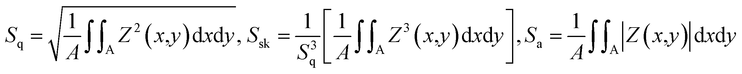
Dielectric theory explores the characteristics of insulating materials when exposed to an electric field. These materials, which impede electric current, undergo polarization under the influence of the field, causing the separation of positive and negative charges and generating an induced electric dipole moment. Key factors such as dielectric permittivity and tangent loss explain the dielectric properties of a material, influencing its potential applications in the electronic industry by assessing its practicality and performance. The dielectric permittivity has been calculated using the notation εr = Cp/Co, where Co = εoA/t, εo = 8.85 × 10⁻¹² F m−1 known as free space permittivity, t = thickness of the pellet, and A = area of cross-section of the electrode.26,27 Fig. 3(a) and (b) depict the variation of relative permittivity (εr) and tangent loss (tanδ) across various ranges of frequencies and temperatures. A common characteristic of dielectric materials is that their dielectric properties diminish as the frequency increases. Multiple forms of polarization exist in the lower-frequency region of the material. In contrast, electronic polarization becomes more prominent in the higher-frequency range. The decrease in εr and tanδ is explained using the two-layer models proposed by Maxwell and Wagner, with Koop's theory playing a role in defining this decreasing pattern.28 Following this theory, a dielectric material consists of two distinct layers: one characterized by poorly conductive grain boundaries and the other by conductive grains. At lower frequencies, electrons exhibit increased reactivity at the grain boundaries, whereas in the grain part, the electrons have become more active at higher frequencies. The high resistance observed at grain boundaries necessitates substantial energy to induce charge carriers to become mobile, particularly in the low-frequency range.
 | ||
| Fig. 3 (a) Frequency dependence of εr, (b) frequency-dependent tanδ, (c) temperature dependence of εr, and (d) temperature-dependent tanδ. | ||
As seen in Fig. 3(a), the value was higher in the lower frequency region and became saturated at the higher region of frequency spectra. In higher frequency regions, there is a clear indication of electronic polarization in the material.
Fig. 3(b) illustrates a shift of the relaxation peaks towards the higher-frequency range, corresponding to an ionic hopping mechanism involving the movement of ions from one site to another. This shift is attributed to a reduced relaxation time.29 The peak changes towards higher frequencies, indicating that the material displays relaxor behavior as the frequency increases. Fig. 3(c) and (d) illustrate the dielectric parameters at various frequencies, ranging from 1 kHz to 1 MHz. With the temperature rise, the εr value rapidly increases (≥32000). The high value of εr indicates colossal dielectric response (CDR). In Fig. 3(d), The tanδ experiences a sudden rise at a low frequency of 1 kHz as the temperature increases. This phenomenon is attributed to oxygen deficiencies in the material, which become more pronounced with the rise in temperature.
With the rise in temperature, a sudden decrease in loss factor value provides a small contribution to the relaxation process. The high value of tanδ at higher temperatures is caused by the rise in polarization with the influence of the mobility of charged ions and charge accumulation at grain boundaries. The property of excellent dielectric materials may be characterized by decreasing dielectric loss with increasing frequency.30
3.4 Conductivity spectra study
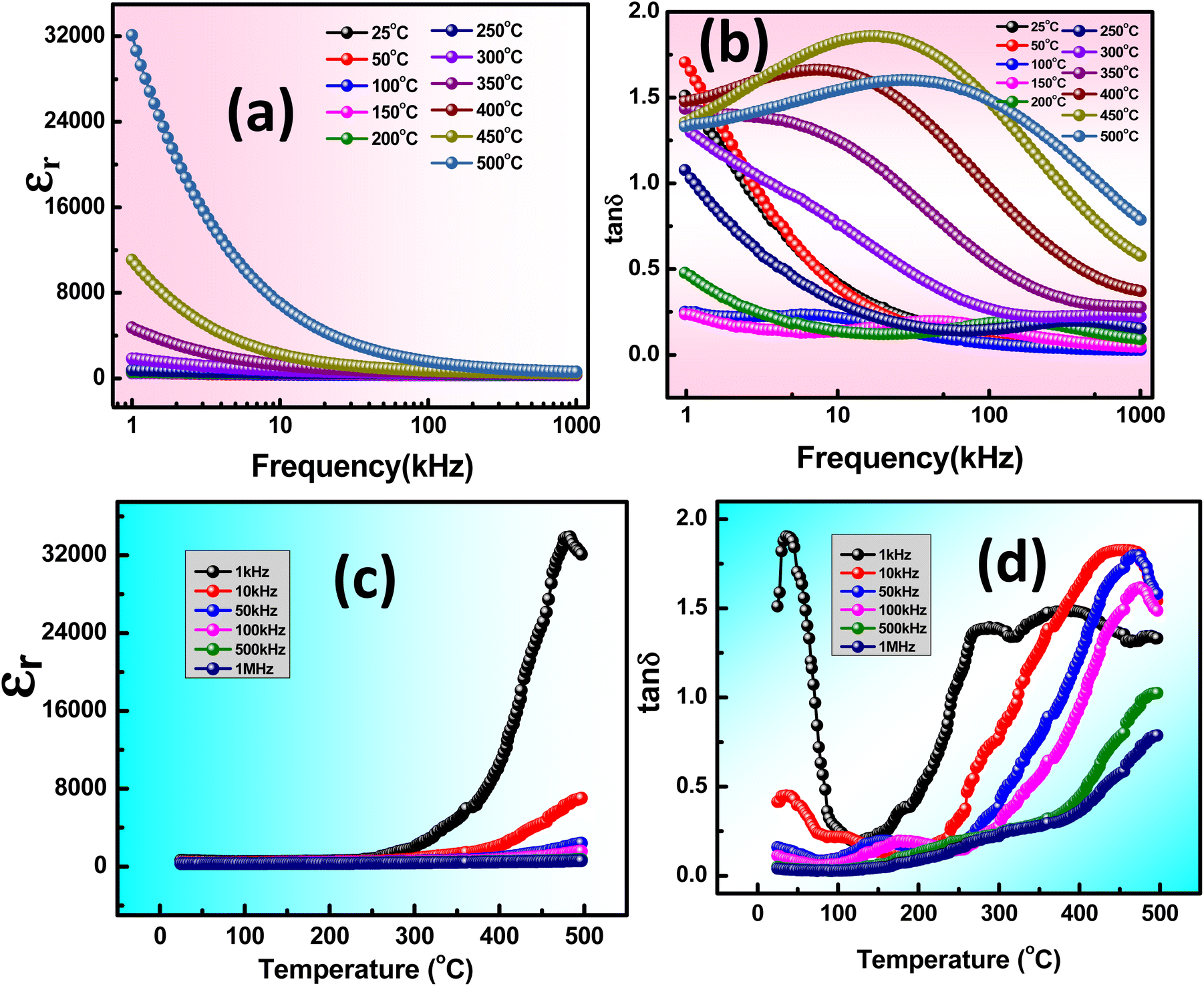
Electrical conductivity analysis is crucial in material research because it discloses the real mechanism that drives the conduction process, which is concealed in dielectric analysis. Due to the poor mobility of charge carriers, conductivity in materials often results from the hopping process between donor and acceptor atoms, which is a temperature-dependent phenomenon. When an external alternating current field is present, weakly bound charge carriers diffuse into the dielectric sample, speeding up the conductivity mechanism. Once more, charge carriers, including anions, cations, polarons, electrons, and defects, play a major role in the process of conductivity in a substance.31 Various types of material (i.e., conductors, insulators, semiconductors) can also be explained based on the charge carrier diffusion mechanism.32This relationship is employed to compute the ac conductance (σac):
| σac = ωεrε0tanδ = 2πfεrε0tanδ |
The universal dielectric response (UDR) allows for the application of Jonscher's Power Law (JPL) to better understand the behavior of σac.33 At lower frequencies, the grain boundaries exhibit increased activity, resulting in limited movement of charged ions. Conversely, the conductive grains are excited at higher frequencies as electronically charged ions start to hop, leading to enhanced charge conduction. The decrease in the material's barrier characteristics with rising temperature likely contributes to the higher ac conductivity observed at higher frequencies, as shown in Fig. 4(a). According to Jonscher's law, both AC and DC conductive may influence the material across a range of lower to higher frequencies.
| σT = σdc+σac = σdc + BωS |
 | ||
| Fig. 4 (a) Frequency-dependent σac, (b) temperature-dependent σdc, and (c) variation of s with increase in temperature of KBFMO material. | ||
B and s represent the polarizability factor and hopping frequency exponent in this context. Jonscher's power law postulates that a plateau in the high-frequency range may result from both direct current (DC) and alternating current (AC) conductivity effects in the sample. Conversely, the lower-frequency plateau region is attributed to DC conductivity.34 Furthermore, the behavior of dc conductivity (σdc) concerning temperature is illustrated in Fig. 4(b). This can be explained by the formula  , where kB denotes Boltzmann's constant, and Ea and σ0 represent the activation energy and pre-exponential factor, respectively. The activation energy (0.123 eV) is determined from the Fig. 4(b).35
When the hopping frequency exponent s equals one, it approaches a purely Debye condition. However, if s falls within the range of 0 to 1, it signifies a non-Debye type of transport mechanism. The increased value of s with the increase in temperature in Fig. 4(c) indicates the presence of non-overlapping small polaron tunneling (NSPT) conduction phenomena, where the decreasing value of s with the increase in temperature caused by the correlated barrier hopping (CBH) model. CBH and NSPT mechanisms are appropriate for the conduction phenomena in the material.36
Fig. 5(a) displays the σac changes with the reciprocal of the absolute temperature (expressed as 1000/T) at 1 MHz frequency. The observed variation in σac across the examined temperature range is the high-temperature intrinsic region. P-type conductivity has similar phenomena for the conduction of charges. The acceptor level (EA) is situated within the energy gap, slightly above the edge of the valence band. When acceptors begin to ionize at lower temperatures, holes migrate to move the uppermost of the valence band and become free carriers. At higher temperatures, the slope becomes −Eg/2 KB. Here, Eg signifies the band gap of the material, and KB denotes the Boltzmann constant, respectively.37 The Fermi level (EF) is positioned within the ionization region between the acceptor levels and the valence band. Conversely, the intrinsic region shifts towards the midpoint between the conduction and valence bands. The values for the band gap is determined by examining the slopes of the ac conductivity at higher temperature region, i.e. Eg = 0.422 eV. With the obtained values for the band gap, an energy band diagram has been constructed for the 1 MHz frequency region, as illustrated in Fig. 5(b).
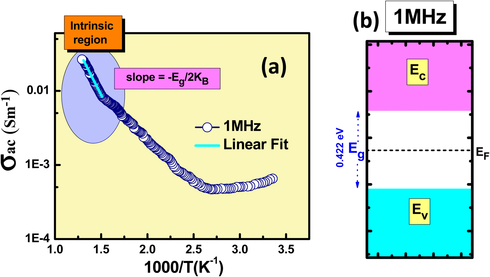 | ||
| Fig. 5 (a) σacvs. 1000/T plot, and (b) energy band diagram of the KBFMO material at 1 MHz frequency. | ||
3.5 Impedance spectra analysis
Impedance spectroscopy is employed to investigate how its microstructure influences the electronic features of the material across a broad spectrum of frequencies and temperatures. It enables the identification of electrically active regions within the sample, including the grains, grain boundaries, and interfaces. In this analysis, both the imaginary and real components of impedance spectra are examined.| Z* = |Z|cosθ − j|Z|sinθ |
| = Z′ + jZ′′ |
Fig. 6(a) depicts the real component Z′, which exhibits higher values at lower frequencies and gradually decreases as frequency increases until it reaches a stable value at a higher frequency region. The frequency-dependent Z′ in the lower range may be attributed to this region's high resistivity stemming from resistive grain boundaries. In contrast, the higher frequency range demonstrates behavior independent of frequency.38 However, as the frequency increases across all temperatures within the higher frequency range, the Z′ value stabilizes and remains constant. This trend in Z′ signifies the dispersion of space charges, which occurs due to the diminishing barrier properties within the material.39 A comparable pattern in Z′′ (the imaginary part) with various frequency ranges is displayed in Fig. 6(b), indicating the existence of space charge polarization at lower frequencies with relaxor nature.40
 | ||
| Fig. 6 (a) Frequency-dependent Z′, (b) frequency-dependent Z′′, and (c) Nyquist plot of KBFMO material. | ||
Between 25 °C and 100 °C, a singular peak is consistently observed in the experimental frequency range, indicating the prevalence of the relaxation mechanism linked to the grain in the sample. The frequency corresponding to the peak is termed the relaxation frequency at the given temperature. As the temperature rises, the curves progressively widen, and the relaxation frequency shifts to a higher frequency. This shift, deviating from pure Debye-type relaxation, is a result of variations in grain size and relaxation time distribution within the ceramic sample.
In the temperature range of 25–500 °C, Fig. 6(c) shows the Nyquist plot (variation of Z′ with Z′′). The Nyquist plot elaborates on the presence of grain, grain boundary, and electrode effect in the material.41,42 The ZSIMPWIN(2.0) relates the experimentally perceived values with the fitted observed values. In this spectrum, the semicircular spectrum was observed after an increase in temperature. Different combinations of RC circuits are fitted in the Nyquist spectra. The fitted circuit and the assessment result are admirable matches with CQR-CR and CQR-CQR circuits. The semicircular behavior of impedance spectra also suggests the material possesses a semiconducting behavior.
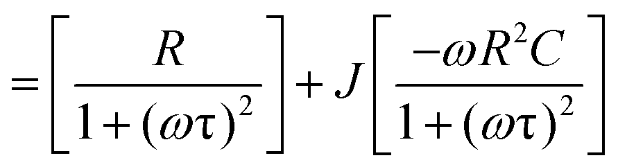
3.6 Modulus spectra study
Modulus spectroscopy is essential in the study of material characteristics in electronic devices, spanning different temperatures and frequencies. Examining storage modulus (reflecting elasticity) and loss modulus (indicating viscosity) offers valuable insights into material responses to stress and strain at various temperature levels. This analysis is critical for enhancing device performance in diverse environmental settings. The technique proves crucial in comprehending frequency-dependent behaviors facilitating the customization of materials for specific electronic applications. Considering the influence of temperature on material properties, modulus spectroscopy guarantees that electronic devices uphold their structural integrity and functionality across a spectrum of temperature variations.The complex modulus spectra are obtained through mathematical calculations using impedance data. This can be expressed as follows mathematically:
| M* = M′ + jM′′ |
| = −ωC0Z′′+ ωC0Z′ |
| = ωC0[ωR2C/(1+ (ωτ)2)] + ωC0[R/(1+ (ωτ)2)] |
 | ||
| Fig. 7 Frequency-dependent (a) real modulus (M′) and (b) imaginary modulus (M′′) at various temperatures, (c) M′ vs. M′′, and (d) relaxation time-dependent inverse absolute temperature of KBFMO material. | ||
The M′ curves approach a finite value, almost zero, at lower frequencies and tend to stabilize at higher frequencies, regardless of temperature. The low-frequency characteristic suggests that ion vibration/oscillation is restricted within the confines of their potential energy wells. As frequency increases, ionization energy decreases, leading to a higher probability of hopping over the potential well. However, at very high frequencies (above 1 MHz), the inertial resistance of ions to rapid electric field oscillation causes the M′ of the sample under study to become insensitive to the electric field.
The conduction mechanism and relaxation characteristics can be examined by studying the imaginary modulus curves with frequency, as Fig. 7(b) depicts. The shift in the position of the M′′ peak with temperature indicates the thermally activated relaxation. The absence of overlapping curves also suggests that the relaxation mechanism deviates from Debye type mechanism.
Furthermore, the observation of merged curves at lower and higher frequency regions is likely attributable to reduced interfacial charges.43Fig. 7(c) illustrates the presence of semicircular arcs within the material, representing the contribution of the grain. This characteristic signifies the semiconductor nature of the material and its thermally activated conduction mechanism. In Fig. 7(d), the slope of the logarithmic relaxation time (τ) plotted against 1000/T can be employed to calculate the Ea using the equation: τ = τ0 * exp (Ea/KBT). The reduction in relaxation time is associated with the hopping mechanism, and the determined activation energy is 0.901 eV.
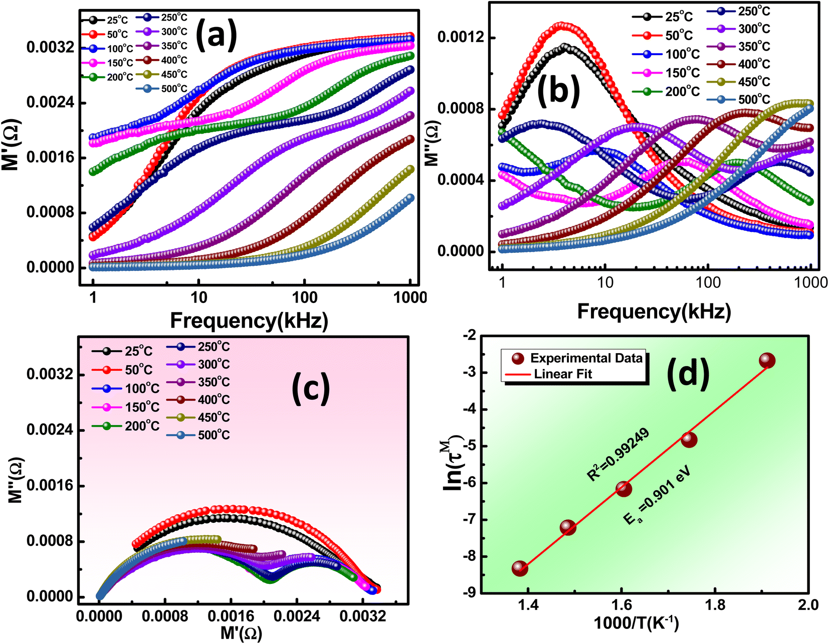
3.7 Temperature variable-resistance study
A thermistor sensor operates based on the principle that resistance changes in response to temperature variations. There are two categories of thermistors: one with resistance that increases as temperature rises, known as a PTC (positive temperature coefficient) thermistor, and the other with resistance that decreases as temperature increases, known as an NTC (negative temperature coefficient) thermistor. This section delves into the analysis of how resistance changes with temperature. In Fig. 8(a), the resistance behavior is depicted over a temperature range from 200 °C to 500 °C (473 K to 773 K). As temperature increases, the resistance value decreases, demonstrating the characteristics of NTCR behavior.44 | ||
| Fig. 8 (a) Temperature-dependent resistance behavior, and (b) Ln(R) vs. 1/T of KBFMO material. | ||
To understand the operation of thermistors, certain physical parameters such as the temperature coefficient of resistance (TCR) and thermistor constant (β) need to be determined, as outlined in ref. 45. The thermistor constant can be derived using the following relationship;
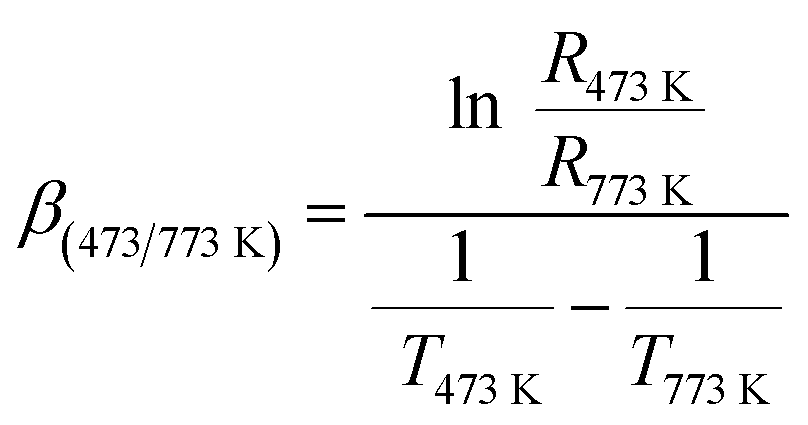
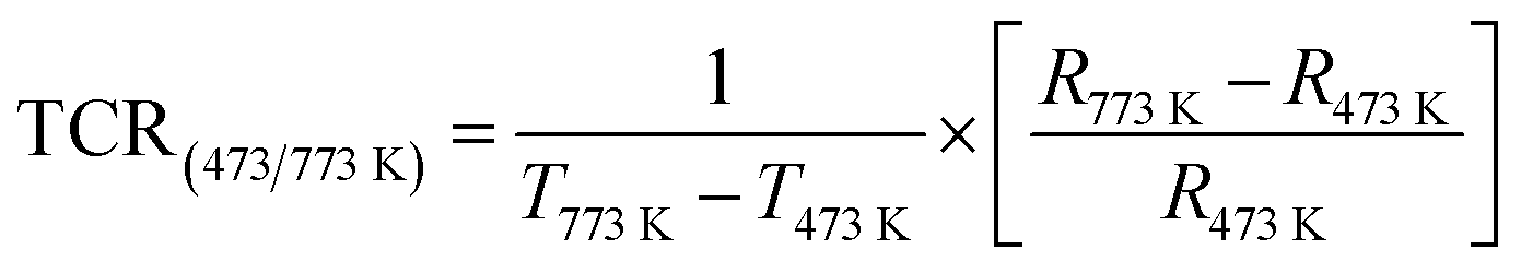
R 473 K and R773 K represent the initial (473 K) and final (773 K) resistances, while T473K and T773 K denote the initial (473 K) and final (773 K) temperatures, respectively. The thermistor constant (β) is determined to be 4633.86, and the temperature coefficient of resistance (TCR) is −0.00322. In Fig. 8(b), the temperature impact on logarithmic resistance is investigated, exhibiting a linear relationship. This demonstrates that the logarithm of electrical resistivity decreases consistently as temperature increases, indicating that the sample is an outstanding candidate for NTC thermistor and is well-suited for use in thermistor-based sensors.46 Ceramics that exhibit NTCR characteristics have practical applications as NTC thermistors. These thermistors are predominantly employed as inrush current limiters (ICL) in electronic devices, preventing abrupt surges of current when powered on devices. The NTCR property of the material is advantageous in safeguarding devices against excessive current during startup. While fixed-resistance materials can restrict inrush currents, they tend to result in power loss and can impact device performance and longevity. On the other hand, NTC thermistors initially have high resistance at lower temperatures (i.e., T = 473 K), which gradually drops as temperature rises, effectively reducing power loss.
3.8 Leakage current and current–voltage analysis
An in-depth examination of the current (I) and voltage (V) behavior in dielectrics is determined through I–V plots. Varistors, also known as voltage-dependent resistors, display non-linear current–voltage characteristics resembling diodes. These components are frequently used for circuit protection against transient voltage surges. They initially maintain high resistance until reaching the threshold voltage (Vt). At this point, they rapidly transition from a high resistance state (HRS) to a low resistance state (LRS), facilitating instantaneous conduction, as depicted in Fig. 9(a). Charge carrier transport in a dielectric within a metal insulator metal (MIM) structure depends on intrinsic properties linked to metal oxides and extrinsic interface factors. Key factors influencing intrinsic transport include defects, trap sites, trap levels, sample relaxation, and density of states. The interface effect, however, is mainly influenced by potential energy barriers, barrier thickness, and charge carrier nature.47 | ||
| Fig. 9 (a) Current dependent voltage plot, (b) logJ vs. E, and (c) logJ vs. logE of KBFMO material. | ||
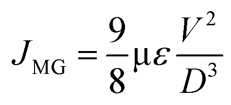
The correlation between current density (J) and electric field (E) can be utilized to ascertain the appropriate mechanism governing leakage current (LC) conduction, as shown in Fig. 9(b). This enables a comprehensive exploration of the LC behavior. For the analysis of various factors contributing to the LC characteristics of the material, a logarithmic scale graph of E versus J has been plotted, as depicted in Fig. 9(c). The power-law connection between J and E represented as Eα Jn, with n = 1, indicates ohmic conduction, while n ≤ 2 suggests space charge limited conduction (SCLC). The total current density (Jtotal) results from both SCLC and ohmic mechanisms present in low and high field regions, expressed as Jtotal = Johm + JSCLC.
Space charge limited conduction (SCLC) eventually reaches a saturation point known as the trap-free Mott-Gurney (M.G.) limit at higher voltages when trap states are occupied and cease to impact carrier conduction. A similar SCLC model applied to a trap-free dielectric is referred to as the M.G. law,48–50 which is expressed as follows:
4. Conclusion
The defect brownmillerite material KBiFeMnO5 is synthesized via a solid-state reaction method. The Monte Carlo method with Le-Bail refinement of the XRD pattern shows the presence of monoclinic symmetry. The grain appearance and strong stiffness on the surface of the material, with a surface topographic analysis, fractal analysis, and isotropy value of 77.43%, are investigated by scanning electron microscope. The study of dielectric behavior supports the presence of Maxwell–Wagner-type dispersion. With the rise in temperature, the εr value rapidly increases (≥32000). The high value of εr indicates a colossal dielectric response (CDR) of the material. The value of the tangent loss is approximately 0 > 2, indicating the high-quality factor of the material. A brief study of AC conductivity and modulus spectra confirms the existence of non-overlapping small polaron tunneling (NSPT), correlated barrier hopping (CBH) conduction mechanisms, and semiconductor-like characteristics. The slope of electric field (E) and current density (J) is 1.372, and 1.371 specifies ohmic conduction, whereas the slope of 3.52 at 25 °C confirms the SCLC conduction mechanism of the synthesized material. The resistance variance temperature analysis reveals that the prepared material is a good applicant for high-temperature NTC thermistor applications.
Conflicts of interest
The authors confirm that the research presented in this work has not been influenced by any known financial conflicts of interest or close personal ties.Acknowledgements
The authors wish to extend their gratitude and sincere thanks to our hosting institution for supplying XRD and SEM characterizations.References
- A. R. Jayakrishnan, A. Kumar, S. Druvakumar, R. John, M. Sudeesh, V. S. Puli, J. P. B. Silva, M. J. M. Gomes and K. C. Sekhar, J. Mater. Chem. C, 2023, 11, 827–858 RSC.
- A. K. S. Chauhan, V. Gupta and K. Sreenivas, Mater. Sci. Eng., B, 2006, 130(1–3), 81–88 CrossRef CAS.
- D. Damjanovic, Rep. Prog. Phys., 1998, 61(9), 1267 CrossRef CAS.
- R. Jain, A. K. S. Chauhan, V. Gupta and K. Sreenivas, J. Appl. Phys., 2005, 97(12), 124101 CrossRef.
- N. Setter, D. Damjanovic, L. Eng, G. Fox, S. Gevorgian, S. Hong and S. Streiffer, J. Appl. Phys., 2006, 100(5), 051606 CrossRef.
- K. Sharma and A. Singh, Journal of Nanoscience and Technology, 2016, 2, 85–90 Search PubMed.
- C. Didier, J. Claridge and M. Rosseinsky, J. Solid State Chem., 2014, 218, 38–43 CrossRef CAS.
- A. Kumar, T. K. Mandal and H. C. Kandpal, In Proceedings of the eight DAE-BRNS interdisciplinary symposium on materials chemistry, 2021, vol. 53, p. 36 Search PubMed.
- J. E. Auckett, A. J. Studer, N. Sharma and C. D. Ling, Solid State Ionics, 2012, 225, 432–436 CrossRef CAS.
- J. Young and J. M. Rondinelli, Phys. Rev. B, 2015, 92(17), 174111 CrossRef.
- K. Chandrakanta, R. Jena, D. P. Sahu and A. K. Singh, J. Alloys Compd., 2023, 938, 168432 CrossRef CAS.
- D. S. Vavilapalli, R. G. Peri, B. Muthuraaman, K. Sridharan, M. R. Rao and S. Singh, Phys. B, 2023, 648, 414411 CrossRef CAS.
- D. Panda, S. S. Hota and R. N. P. Choudhary, In 2023 International Conference in Advances in Power, Signal, and Information Technology (APSIT), IEEE, 2023, pp. 25–28 Search PubMed.
- H. Deng, M. Zhang, Q. Zhong, J. Wei and H. Yan, Ceram. Int., 2014, 40(4), 5869–5872 CrossRef CAS.
- D. Varshney, A. Kumar and K. Verma, J. Alloys Compd., 2011, 509(33), 8421–8426 CrossRef CAS.
- B. Dhanalakshmi, K. Pratap, B. P. Rao and P. S. Rao, J. Alloys Compd., 2016, 676, 193–201 CrossRef CAS.
- T. Chakraborty, R. Yadav, S. Elizabeth and H. L. Bhat, Phys. Chem. Chem. Phys., 2016, 18, 5316–5323 RSC.
- A. Altomare, C. Cuocci, C. Giacovazzo, A. Moliterni, R. Rizzi, N. Corriero and A. Falcicchio, J. Appl. Crystallogr., 2013, 46, 1231–1235 CrossRef CAS.
- A. Le Bail, Powder Diffr., 2004, 19(3), 249–254 CrossRef CAS.
- J. T. Zhang, X. M. Lu, J. Zhou, J. Su, K. L. Min, F. Z. Huang and J. S. Zhu, Phys. Rev. B, 2010, 82(22), 224413 CrossRef.
- B. Khan, M. K. Singh, A. Kumar, A. Pandey, S. Dwivedi, U. Kumar and S. C. Roy, J. Alloys Compd., 2022, 893, 162225 CrossRef CAS.
- D. Panda, S. S. Hota and R. N. P. Choudhary, Phase Transitions, 2023, 96(11), 822–839 CrossRef CAS.
- S. S. Hota, D. Panda and R. N. P. Choudhary, Inorg. Chem. Commun., 2023, 153, 110785 CrossRef.
- D. Panda, S. S. Hota and R. N. P. Choudhary, J. Mater. Sci.: Mater. Electron., 2023, 34(27), 1908 CrossRef CAS.
- S. S. Hota, D. Panda and R. N. P. Choudhary, Solid State Ionics, 2023, 399, 116313 CrossRef CAS.
- S. N. Das, S. K. Pardhan, S. Bhuyan, S. Sahoo, R. N. P. Choudhary and M. N. Goswami, J. Electron. Mater., 2018, 47, 843–854 CrossRef CAS.
- A. Tripathy, S. N. Das, S. K. Pradhan, S. Bhuyan and R. N. P. Choudhary, J. Mater. Sci.: Mater. Electron., 2018, 29, 4770–4776 CrossRef CAS.
- D. S. Kumar, K. C. B. Naidu, M. M. Rafi, K. P. Nazeer, A. A. Begam and G. R. Kumar, Mater. Sci.-Pol., 2018, 36, 123–133 CAS.
- A. Arya and A. L. Sharma, J. Mater. Sci.: Mater. Electron., 2018, 29(20), 17903–17920 CrossRef CAS.
- K. Parida, S. K. Dehury and R. N. P. Choudhary, Chin. J. Phys., 2019, 59, 231–241 CrossRef CAS.
- P. Gupta, P. K. Mahapatra and R. N. P. Choudhary, Phys. Status Solidi B, 2020, 257(1), 1900236 CrossRef CAS.
- T. Zheng and J. Wu, J. Mater. Chem. C, 2015, 3(43), 11326–11334 RSC.
- J. P. Tiwari and K. Shahi, Philos. Mag., 2007, 87(29), 4475–4500 CrossRef CAS.
- M. Yildirim and A. Kocyigit, Surf. Rev. Lett., 2020, 27, 1950217 CrossRef CAS.
- D. C. Sinclair and A. R. West, J. Appl. Phys., 1989, 66, 3850–3856 CrossRef CAS.
- D. Panda, S. S. Hota and R. N. P. Choudhary, Mater. Sci. Eng., B, 2023, 296, 116616 CrossRef CAS.
- S. Lenka, T. Badapanda, P. Nayak, S. Sarangi, S. Anwar and S. N. Tripathy, J. Mol. Struct., 2023, 1274, 134413 CrossRef CAS.
- S. A. Ansari, A. Nisar, B. Fatma, W. Khan and A. H. Naqvi, Mater. Sci. Eng., B, 2012, 177(5), 428–435 CrossRef CAS.
- Y. Iqbal, W. H. Shah, B. Khan, M. Javed, H. Ullah, N. Khan and A. Safeen, Phys. Scr., 2023, 98(6), 065951 CrossRef.
- K. Kumari, K. Prasad and R. N. P. Choudhary, J. Alloys Compd., 2008, 453(1–2), 325–331 Search PubMed.
- G. A. Kaur, S. Kumar, V. Sharma, I. Kainthla, S. Thakur, S. Thakur and M. Shandilya, Inorg. Chem. Commun., 2023, 151, 110644 CrossRef.
- M. Kamran, Y. Abbas and M. Anis-ur-Rehman, Inorg. Chem. Commun., 2023, 155, 111034 CrossRef CAS.
- B. Pati, R. N. P. Choudhary and P. R. Das, J. Alloys Compd., 2013, 579, 218–226 CrossRef CAS.
- M. H. Yan, G. T. Miao, G. J. Bai, P. Li, J. G. Hao, W. Li and P. Fu, J. Alloys Compd., 2023, 937, 168453 CrossRef CAS.
- C. Chen, Measurement, 2009, 42(7), 1103–1111 CrossRef.
- S. S. Hota, D. Panda and R. N. P. Choudhary, in 2023 International Conference in Advances in Power, Signal, and Information Technology (APSIT), IEEE, 2023, pp. 1–6 Search PubMed.
- E. W. Lim and R. Ismail, Electronics, 2015, 4(3), 586–613 CrossRef CAS.
- M. Zubair, N. Raheem, M. Q. Mehmood, Y. S. Ang and Y. Massoud, Phys. Plasmas, 2023, 30, 042112 CrossRef CAS.
- D. Panda, S. S. Hota and R. N. P. Choudhary, Inorg. Chem. Commun., 2023, 158(1), 111501 CrossRef CAS.
- L. I. Breen, A. M. Darr, A. M. Loveless, K. L. Cartwright and A. L. Garner, In 2022 IEEE International Conference on Plasma Science (ICOPS) IEEE, 2022, pp. 1–2 Search PubMed.
| This journal is © The Royal Society of Chemistry 2024 |