DOI:
10.1039/D3RA08447G
(Paper)
RSC Adv., 2024,
14, 6058-6063
Low voltage-driven, high-performance TiO2 thin film transistors with MHz switching speed†
Received
11th December 2023
, Accepted 18th January 2024
First published on 16th February 2024
Abstract
High-speed circuits based on thin film transistors (TFTs) show promising potential applications in biomedical imaging and human–machine interactions. One of the critical requirements for high-speed electronic devices lies in high-frequency switching or amplification at low voltages, typically driven by batteries (∼3.0 V). To date, however, most electrical performances of metal oxide TFTs are measured under direct current (DC) conditions, and their dynamic switching behaviour is scarcely explored and studied systematically. Here in this work, we present low voltage-driven, high-performance TiO2 thin film transistors, which can be operated at a switching speed of MHz. Our proposed TiO2 TFTs demonstrated a high on–off ratio of 107, together with a subthreshold swing (SS) of ∼150 mV Dec−1 averaged over four orders of magnitude, which can be further reduced below 100 mV Dec−1 when the temperature cools to 77 K. Additionally, the TiO2 TFTs exhibit excellent gate-pulse switching at various frequencies ranging from 1.0 Hz to 1.0 MHz. We also explored the potential application of the TiO2 TFTs as logic gates by constructing a resistive-loaded inverter, which shows stable operation at 10 kHz frequency and various temperatures. Thus, our results show the great potential of TiO2 TFTs as a new platform for high-speed electronic applications.
1. Introduction
Thin film transistors (TFTs) have attracted much interest due to their ever-growing application in liquid-crystal matrix displays and radio frequency identification tags.1–3 Typically, polycrystalline and amorphous silicon thin films have been used as the semiconducting layer thanks to their material abundance in nature and mature fabrication process. However, the low electron mobility and non-transparency in the visible range of (polycrystalline and amorphous) silicon thin films hinder further development, for instance, as portable electronics driven by battery-supplied voltages.4–6 Thus, metal-oxide semiconductors, such as TiO2, ZnO, InGaZnO, and InZnO, have emerged as promising alternatives with their outstanding properties including larger energy bandgap, higher electron mobility, optical transparency, and better film uniformity.7–11 In particular, titanium oxide (TiO2) has shown great potential as an active channel material in n-type TFTs owning to its superior advantages such as low cost, material abundance, non-toxicity, and mechanical stability. Although tremendous efforts have been devoted to improving the electrical performance of TiO2 TFTs operated at battery-supply voltages, most electrical performances of TiO2 TFTs have been focused on DC operation, and the corresponding dynamic switching behaviour is typically ignored and not reported as a figure of merit.12–14 In recent years, high-speed circuits based on thin film transistors have shown promising potential applications in biomedical imaging and human–machine interactions.15–17 In this regard, it is crucial to implement reliable, stable, and high-speed switching thin film transistors with a sufficiently high on/off ratio, an acceptable carrier mobility, and a low-driven voltage.
In this paper, we fully investigate the static DC performance and dynamic switching behaviour of the proposed TiO2 thin film transistors including on–off ratios as high as 107, subthreshold swings of averaged 150 mV Dec−1 (four orders of magnitude), a contact resistance of 0.13 Ω cm2, an effective mobility of 3.87 cm2 V−1 s−1, and a gate-pulse switching frequency beyond 1.0 MHz. Furthermore, the potential application of the TiO2 TFTs as logic gates is explored via the construction of a resistive-loaded inverter, which can operate at 10 kHz frequency with a gain of 4.8 V V−1. Our work shows a tremendous potential of TiO2 TFTs as fast-switching speed matrix displays and high-speed logic operations.
2. Experimental
2.1 Device fabrication
Fig. S1† illustrates the stepwise fabrication process flow and the corresponding cross-section schematic for TiO2 thin film transistors. The TiO2 thin film transistors were fabricated using Si–SiO2 substrates and the thickness of SiO2 dielectric is 285 nm. Thermally activated atomic layer deposition (ALD) was then utilized to deposit TiO2 as channel materials, which was then annealed at 500 °C for 30 min in an oxygen atmosphere for better thin film quality. The TiO2 layer was deposited at a relatively low temperature (∼250 °C) and its thickness was controlled by the cycling loops (0.12 nm for each cycle). TiO2 strips were then etched using the ICP dry etching system and CF4/Ar mixture was used as the etching gas. The etched region was defined by a standard photo-lithography procedure using a direct laser writer. AZ1500 photoresist was spin-coated and the baking temperature was 100 °C for 1 min. Another photo-lithography step was repeated to define the source and drain areas, and double layers of metal Al/Pt (50/30 nm) were then sputtered onto the substrate. Al was selected as the contact metal since a good ohmic contact can be formed between Al and TiO2 annealed at 450 °C for 5 min, while Pt is used as a capping layer to prevent the Al layer from oxidization.18 A layer of Al2O3 dielectric with a thickness of 8 nm was chosen as the insulating gate oxide, which was deposited by plasma-enhanced ALD technique at a low temperature of 350 °C. Finally, the top gate region was defined by another photo-lithography step and double layers of Ti/Pt (10/50 nm) were then deposited as contact metals. To improve the quality of the TiO2/Al2O3 interface, the fabricated devices are annealed at 400 °C for 30 min (Ar/H2). The thickness of each layer is labeled accordingly in the corresponding cross-section illustrations.
2.2 Material characterization
To investigate the TiO2 film quality as the channel material, the X-ray diffraction technique, and the optical ellipsometry measurement were utilized to characterize the crystalline phase, film thickness, and uniformity. X-ray diffraction (XRD) was performed via Empyrean equipment, and the 2 theta linearity over the whole range is equal to or better than ±0.1°. The optical ellipsometry measurement was conducted by an imaging Ellipsometer Nanofilm-ep4 (spectral range: 250–1700 nm). The highest lateral resolution of Nanofilm-ep4 is around 300 nm, which can be used to measure the thickness and the optical index over the smallest area of 1 μm2. Raman spectra were collected via LabRAM HR Evolution Confocal Raman Microscope. The wavelength of the scanning laser is located at 325 nm, and the Raman shift ranges from 100 cm−1 to 800 cm−1. X-ray photoelectron spectroscopy (XPS) measurement of TiO2 thin film before and after O2 annealing was conducted using Thermo Fisher ESCALAB XI+ and the incident energy of X-ray (Al Kα) is set to be 1486.6 eV, which allows high-resolution surface element analysis. The surface roughness of TiO2 thin film was visualized using atomic force microscopy (AFM, Cypher S/Oxford Instruments Asylum Research) and the corresponding profile images were collected at an area of 1 × 1 μm2 under fast scan mode. All the material characterization was conducted at room temperature and atmosphere.
2.3 Electrical measurement setup
The electrical measurement was performed within a six-arm low-temperature Lakeshore vacuumed probe station, which consists of four DC probes and two high-frequency tips. The available temperature range starts from 77 K to 350 K. The temperature-dependent electrical data was collected when the chamber heated up for higher temperature accuracy. DC probes were directly approached to metallic pads and the silicon substrate was connected to the stage using conductive tapes. The electrical signals were applied and visualized via an Agilent B1500A semiconductor device analyzer, which allows various modes of sweeping I(V), fast I(V) scan, and C(V) measurement. The applied maximum voltage can be up to 200 V with a maximum current of 1 A. The current resolution at room temperature is at the order of a few fA if grounded appropriately. In terms of the fast I(V) scan mode, a waveform-generating module was utilized to apply arbitrary and programmable electrical signals at a pulse width of 10 ns. Meanwhile, the minimum collection speed is limited to 10 ns and it should be noted that the signal noise increases significantly as the collection time shortens. In terms of the dynamic response of resistive-loaded inverters, the input signals were generated via a function generator (Keysight 33500B true form generator), which offers a maximum frequency (∼100 MHz) of square waveforms. At the same time, the fast-switching electrical signals were collected and visualized by a digital bench oscilloscope (Tektronix TBS2074B series). To prevent the electrical propagation loss and crosstalk of high-speed signals, all the electrical connections were connected via broad-bandwidth SMU cables.
3. Results and discussion
3.1 Device schematics and transistor performance at T = 300 K
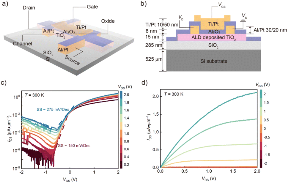
Fig. 1a shows the schematic illustration of TiO2 thin film transistors fabricated on top of SiO2/Si substrates. Thermally activated atomic layer deposition (ALD) was utilized to deposit ∼15 nm TiO2 as channel materials followed by annealing at 500 °C for 30 min in an oxygen atmosphere to improve the crystalline and mobility. Another layer of Al2O3 (∼8 nm) was chosen as the insulating oxide due to its excellent film quality and large bandgap.18–20Fig. 1b illustrates the corresponding cross-section view, where Al was selected as the contact metal since a good ohmic contact can be formed between Al and TiO2 without annealing, while Pt is used as a capping layer to prevent the Al layer from oxidization. In addition, double layers of Ti/Pt (10/50 nm) function as top gate contacts. An overview of device fabrication is well-elaborated in Fig. S1.† The active device area of TiO2 TFTs is 18 (length) × 10 (width) mm2, while the contact pads are designed as 100 × 100 mm2 for probe electrical measurement (Fig. S2†). The film quality and thickness of the annealed TiO2 thin film as channel material were investigated via XRD, Raman, XPS, AFM, and optical ellipsometry techniques, respectively. Our result suggests that the as-deposited TiO2 thin films show an amorphous phase and the formation of anatase polycrystalline phase after O2 annealing was confirmed based on XRD and Raman spectra (Fig. S3†).21,22 Typically, the electron mobility of crystallized TiO2 thin film is much better than the counterpart of amorphous phase due to less traps and lattice scattering.23–25 Meanwhile, the XPS result suggests that the annealing process may remove the defects of non-totally oxidized Ti, therefore improving the crystalline lattice and electron mobility (Fig. S4†).26,27 Furthermore, the thickness and surface uniformity were characterized by optical ellipsometry and AFM technique, where the averaged thickness is 15.8 ± 0.4 nm (Fig. S5†) and surface roughness is around 0.3 nm (Fig. S6†).
 |
| | Fig. 1 Device schematics and transistor performance. (a) Schematic illustration of TiO2 thin film transistors and the electrical connection. (b) Cross-section structure diagram with labeled thickness for each layer. (c) Room temperature transfer curves (IDS–VGS) of TiO2 TFTs collected at constant VDS ranging from 0.2 V to 2.0 V at an interval of 0.2 V. (d) Output characteristics (IDS–VDS) as a function of VGS ranging from −2.0 V to +2.0 V in 0.5 V step. | |
Fig. 1c presents the subthreshold characteristics of TiO2 TFTs at various drain-to-source voltages (VDS), where negligible hysteresis window was observed. Our proposed TiO2 TFTs demonstrated a negative turn-on voltage, a significant on–off ratio of 107, and a subthreshold swing (SS) of ∼150 mV Dec−1 averaged over four orders of magnitude at VDS = 0.2 V. The ohmic contact behaviour was confirmed via the transfer length method as shown in Fig. S7† and the specific contact resistivity (ρC) is extracted to be around 0.13 Ω cm2. It is the high contact resistivity that contributes to the low source-to-drain current (IDS) ∼210 nA at VDS = 1.0 V when no gate bias was applied. The gate leakage current density is determined to be lower than 10−6 A cm−2 and the corresponding breakdown voltage is around 4.8 V, suggesting the deposited Al2O3 layer is of good insulating quality over the gate-to-source voltage (VGS) measurement range (Fig. S8b†). Fig. 1d illustrates the collected output (IDS–VDS) curves as a function of VGS, where current saturation and pinch-off are visualized. We noticed that the spacing of output (IDS–VDS) curves measured at VGS = +2.0 V is sub-linear, indicating the possible effect of self-heating. To extract the effective mobility of TiO2 thin film, we have also presented the transfer curve at VDS = 100 mV in Fig. S8d† and the estimated electron mobility is 3.87 cm2 V−1 s−1, comparable to the as-far best-reported value (∼10.7 cm2 V−1 s−1).25
3.2 Temperature-dependent electrical characterization
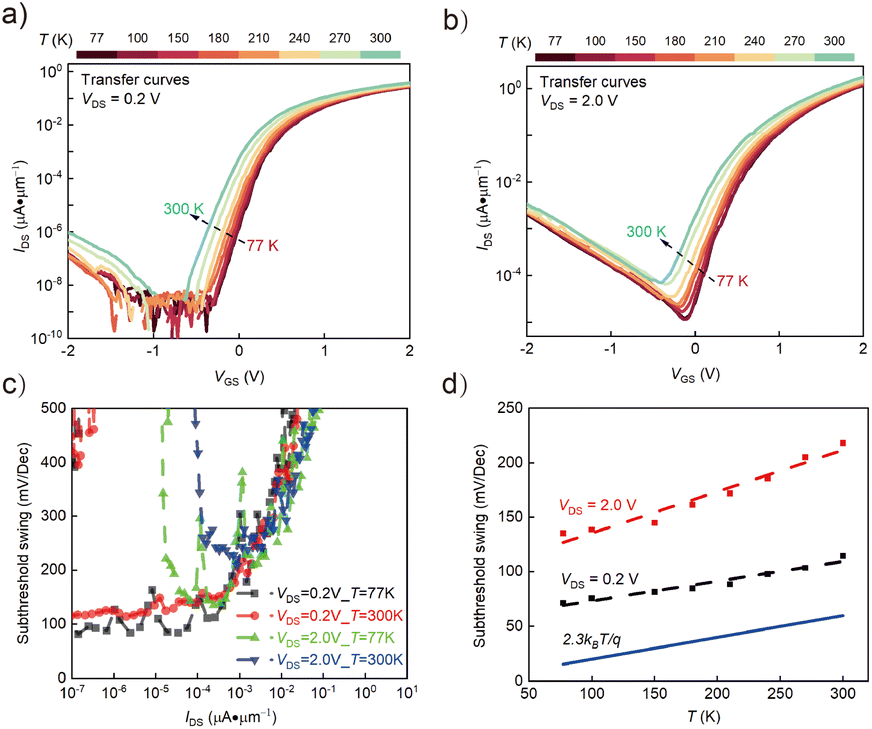
To further elucidate the charge transport process of TiO2 TFTs, we have performed the transfer characteristics at different temperatures ranging from 300 K to 77 K at an interval of 30 K. Fig. 2a and b demonstrate the temperature-dependent subthreshold behaviour measured at VDS = 0.2 V and 2.0 V, respectively. As can be seen, the collected transfer curves become steeper and the corresponding turn-on voltages shift to more positive values when the temperature cools down. In addition, the on–off ratio shows insensitive temperature dependence, which suggests that our proposed TiO2 TFTs can operate at quite broad temperature ranges. Fig. 2c presents the extracted temperature-dependent SS plotted against IDS. The averaged SS extracted over four orders of magnitude decreases from 150 mV Dec−1 at T = 300 K to 100 mV Dec−1 when the temperature cools to 77 K (VDS = 0.2 V). The charge transport mechanism for our TiO2 TFTs is dominated by thermionic emission, therefore, the extracted SS should be linear as a function of temperature.28,29Fig. 2d illustrates the extracted minimum SS plotted against temperature, where the experimentally measured SS scales linearly as a function of temperature as expected and shares a similar slope to the theoretical values following the Boltzmann limitation. Detailed temperature-dependent SS analysis is discussed in ESI Section 9.†
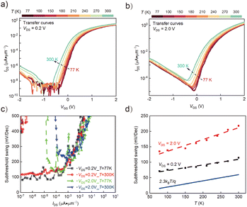 |
| | Fig. 2 Temperature-dependent transistor performance. (a and b) Subthreshold behaviour measured at various temperatures ranging from 77 K to 300 K while the VDS remains constant at 0.2 V and 2.0 V, respectively. (c) SS plotted against IDS at the lowest and highest temperatures (VDS = 0.2 V and 2.0 V). (d) Extracted minimum SS as a function of temperature. The red and black dotted curves represent the experimentally measured values, while the blue line refers to the theoretical value following the Boltzmann limitation (2.3 kBT/q). | |
3.3 Dynamic switching response and transient performance
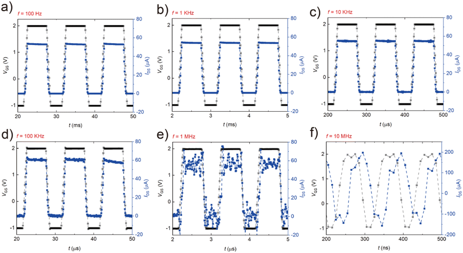
To explore the time-resolved dynamic switching characteristics of TiO2 TFTs, transient time traces of source to drain current (IDS) were analyzed by applying pulsed gate voltages (VGS from −1.0 V to +2.0 V) at constant VDS = +2.0 V. Fig. 3a–f displays different dynamic responses of TiO2 TFTs collected at frequencies ranging from 100 Hz to 10 MHz at a step of one order. To begin with, we observed noise-free and stable currents (IDS) being switched on and off at frequencies below 1.0 MHz. The on and off states of IDS agree well with the previous DC result. Subsequently, Fig. 3e shows that IDS can still be switched on and off, but the noise level of IDS becomes significant at a frequency of 1.0 MHz. The reason may be due to the shorter collection time of each cycle at higher frequencies (the noise level increases significantly when the collection averaging time decreases, especially when the averaging time is shorter than 1 μs). Furthermore, the switching rise time and fall time can be defined as the time elapse when the switched-on current decays from 90% to 10% and vice versa in the transient time trace.30,31 Since the rise time and fall time are both around 100 ns, the maximum switching speed is calculated to be around 5.0 MHz via the following equation
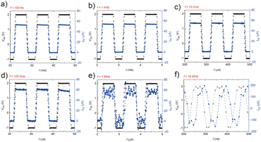 |
| | Fig. 3 Dynamic switching behaviour of TiO2 TFTs. Transient time traces collected at various frequencies by applying pulsed gate voltages (VGS from −1.0 V to +2.0 V) at constant VDS = +2.0 V. (a–f) represent the corresponding time traces collected at different frequencies from 100 Hz to 10 MHz at an interval of one order of magnitude. | |
Finally, the device cannot be switched on and off consistently when the applied frequency exceeds 10 MHz (Fig. 3f) probably due to the response time of the device itself or the limitation of our electrical setup (the collection time should be longer than 10 ns and the noise level becomes significant when the frequency is above 10 MHz). Thus, it requires more effort and higher-speed measurement equipment to estimate the accurate response time in our future work. Notably, our proposed TiO2 TFTs can be switched on and off even at a temperature as low as 77 K (Fig. S10†). The dynamic switching response and transient performance of TiO2 TFTs switch on more opportunities for high-speed electronic devices based on metal oxide TFTs.
3.4 Static and dynamic resistive-loaded inverter characteristics
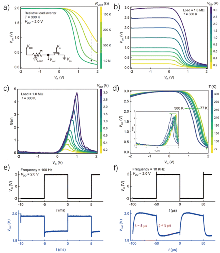
To further explore the potential application of TiO2 TFTs on high-speed circuits, we have constructed a resistive-loaded inverter and studied the static and dynamic transient behaviour. Fig. 4a shows clear voltage transfer curves collected at various resistive loads ranging from 100 kΩ to 1.0 MΩ. The inset illustrates the circuit design with a fixed supply voltage (VDD = 2.0 V). We observed that the output voltages (Vout) can be “pulled down” to near 0 V as the load resistor increases to 1.0 MΩ. Fig. 4b displays the voltage transfer characteristics as a function VDD, where stable and consistent inverting behaviour can be observed at different supply voltages ranging from 0.2 V to 3.0 V. Fig. 4c illustrates the corresponding gain curves, which exhibit a maximum voltage gain of ∼4.8 at VDD = 3.0 V. Notably, the maximum voltage gain shows an insensitive dependence on temperature ranging from 77 K to 300 K, which suggests that the resistive-loaded inverter can operate at a quite broad regime (Fig. 4d). Our proposed TiO2 TFTs may find potential applications as quantum computing components and active backplane matrix operated at cryogenic temperatures. The last section is the dynamic performance of the resistive-loaded inverter, which was evaluated by applying square-waveform input signals with an amplitude of 4.0 V, a 50% duty cycle, no offset voltage, and various frequencies. To visualize the transient behavior, the external resistive load was fixed at 1.0 MΩ. Meanwhile, the fast-switching time traces of output electrical signals were collected and visualized by a digital bench oscilloscope. Fig. 4e and f demonstrate the transient behaviour in response to square-waveform input signals with a frequency of 100 Hz and 10 kHz, respectively. A stable and consistent inverting performance can be observed at different frequencies. In addition, the rise (tr) and fall time (tf) of switching events in Fig. 4f can be fitted by simple exponential functions to estimate the inverter response time.17,32 Both the rise and fall time are calculated to be around 5 ms, thus, the maximum speed of the resistive-loaded inverter is no more than 100 kHz. However, it is noteworthy that this maximum speed is not limited by the device itself but by the resistive-capacitive time constant (RC delay) of the constructed circuit. Table S1† benchmarks the electrical performances and highlights the differences between our proposed TiO2 TFTs and other types of devices. Our work studies systematically the static DC performance, dynamic switching behaviour, and logic gates of resistive-loaded inverters, which paves the way towards forthcoming high-speed and low voltage-driven electronic components based on metal semiconductors.
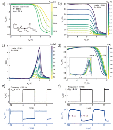 |
| | Fig. 4 Static and dynamic resistive-loaded inverter characteristics. (a) Voltage transfer curves are collected at different resistive loads while the supply voltage remains constant (VDD = 2.0 V). The inset presents the circuit design and electrical connection. (b) Voltage transfer curves as a function of VDD and the resistive load is 1.0 MΩ. (c) Calculated gain curves at different VDD levels ranging from 0.2 V to 3.0 V. (d) Temperature-dependent voltage transfer curves and related gain curves at VDD = 3.0 V and load = 1.0 MΩ. Dynamic behaviour of resistive-loaded inverter in response to square-waveform input signals with a frequency of 100 Hz (e) and 10 kHz (f). The amplitude of input signals is 4.0 V with a 50% duty cycle and the supply voltage is constant at 2.0 V while the resistive load is 1.0 MΩ. | |
4. Conclusions
In summary, we have presented low voltage-driven, high-performance TiO2 thin film transistors, which can be operated at a switching speed of MHz. The static DC performance and dynamic switching behaviour of the proposed TiO2 TFTs are studied systematically. The film quality and thickness of the prepared TiO2 thin film were investigated via XRD, Raman, XPS, AFM, and ellipsometry techniques. Our work shows that there is still plenty of room to explore and improve the switching frequencies of metal oxide thin film transistors, which may find their future application in the next generation of display backplanes and high-speed electronic circuits.
Author contributions
Xiaoping Chen: conceptualization, investigation, formal analysis, methodology, visualization, writing – original draft, writing – review & editing. Jiancong Ni: resources, formal analysis. Weiqiang Yang: investigation, formal analysis. Shaoying Ke: supervision, resources, formal analysis, writing – review & editing. Maosheng Zhang: supervision, resources, conceptualization, formal analysis, writing – review & editing.
Conflicts of interest
There are no conflicts to declare.
Acknowledgements
The authors are grateful to the President's Fund of Minnan Normal University (KJ2021005 and KJ2023002). X. Chen thanks the support under the Natural Science Foundation of Fujian Province, China (Grant No. 2022J05173). S. Ke thanks the support under the National Natural Science Foundation of China under Grant No. 62004087.
References
- K. Myny, Nat. Electron., 2018, 1, 30–39 CrossRef CAS.
- C. D. Dimitrakopoulos and D. J. Mascaro, IBM J. Res. Dev., 2001, 45, 11–27 CAS.
- K. Nomura, H. Ohta, A. Takagi, T. Kamiya, M. Hirano and H. Hosono, Nature, 2004, 432, 488–492 CrossRef CAS PubMed.
- M. J. Powell, IEEE Trans. Electron Devices, 1989, 36, 2753–2763 CrossRef CAS.
- A. Nathan, A. Kumar, K. Sakariya, P. Servati, S. Sambandan and D. Striakhilev, IEEE J. Solid-State Circuits, 2004, 39, 1477–1486 Search PubMed.
- S. D. Brotherton, Semicond. Sci. Technol., 1995, 10, 721 CrossRef CAS.
- R. A. Street, T. N. Ng, R. A. Lujan, I. Son, M. Smith, S. Kim, T. Lee, Y. Moon and S. Cho, ACS Appl. Mater. Interfaces, 2014, 6, 4428–4437 CrossRef CAS.
- Z. Chai, S. A. Abbasi and A. A. Busnaina, ACS Appl. Electron. Mater., 2023, 5, 2328–2337 CrossRef CAS.
- H. Hosono, Nat. Electron., 2018, 1, 428 CrossRef.
- W. Xu, L. Hu, C. Zhao, L. Zhang, D. Zhu, P. Cao, W. Liu, S. Han, X. Liu, F. Jia, Y. Zeng and Y. Lu, Appl. Surf. Sci., 2018, 455, 554–560 CrossRef CAS.
- A. Abliz, L. Xu, D. Wan, H. Duan, J. Wang, C. Wang, S. Luo and C. Liu, Appl. Surf. Sci., 2019, 475, 565–570 CrossRef CAS.
- J. Zhang, M. Jia, M. G. Sales, Y. Zhao, G. Lin, P. Cui, C. Santiwipharat, C. Ni, S. McDonnell and Y. Zeng, ACS Appl. Electron. Mater., 2021, 3, 5483–5495 CrossRef CAS.
- N. Zhong, J. J. Cao, H. Shima and H. Akinaga, IEEE Electron Device Lett., 2012, 33, 1009–1011 CAS.
- J. W. Park, S. W. Han, N. Jeon, J. Jang and S. Yoo, IEEE Electron Device Lett., 2008, 29, 1319–1321 CAS.
- Z. Ying, C. Feng, Z. Zhao, S. Dhar, H. Dalir, J. Gu, Y. Cheng, R. Soref, D. Z. Pan and R. T. Chen, Nat. Commun., 2020, 11, 2154 CrossRef CAS.
- A. F. Paterson and T. D. Anthopoulos, Nat. Commun., 2018, 9, 5264 CrossRef CAS PubMed.
- J. W. Borchert, U. Zschieschang, F. Letzkus, M. Giorgio, R. T. Weitz, M. Caironi, J. N. Burghartz, S. Ludwigs and H. Klauk, Sci. Adv., 2020, 6, eaaz5156 CrossRef CAS.
- F. Wang, Y. Liu, T. X. Hoang, H.-S. Chu, S.-J. Chua and C. A. Nijhuis, Small, 2022, 18, 2105684 CrossRef CAS PubMed.
- F. Wang, T. X. Hoang, H.-S. Chu and C. A. Nijhuis, Laser Photonics Rev., 2022, 16, 2100419 CrossRef CAS.
- X. Liu, K. Pan, Z. Zhang and Z. Feng, Appl. Surf. Sci., 2023, 640, 158337 CrossRef CAS.
- G. Luka, B. S. Witkowski, L. Wachnicki, M. Andrzejczuk, M. Lewandowska and M. Godlewski, CrystEngComm, 2013, 15, 9949–9954 RSC.
- A. T. Hassan, E. S. Hassan and O. M. Abdulmunem, J. Mech. Behav. Mater., 2021, 30, 304–308 CrossRef.
- J. Zhang, P. Cui, G. Lin, Y. Zhang, M. G. Sales, M. Jia, Z. Li, C. Goodwin, T. Beebe, L. Gundlach, C. Ni, S. McDonnell and Y. Zeng, Appl. Phys. Express, 2019, 12, 096502 CrossRef CAS.
- B. Kim, T. Kang, G. Lee and H. Jeon, Nanotechnology, 2022, 33, 045705 CrossRef CAS.
- W. S. Shih, S. J. Young, L. W. Ji, W. Water and H. W. Shiu, J. Electrochem. Soc., 2011, 158, H609 CrossRef CAS.
- Y. Xu, S. Wu, P. Wan, J. Sun and Z. D. Hood, RSC Adv., 2017, 7, 32461–32467 RSC.
- B. Bharti, S. Kumar, H. N. Lee and R. Kumar, Sci. Rep., 2016, 6, 32355 CrossRef CAS PubMed.
- M. Nadeem, I. Di Bernardo, X. Wang, M. S. Fuhrer and D. Culcer, Nano Lett., 2021, 21, 3155–3161 CrossRef CAS PubMed.
- S. Datta, W. Chakraborty and M. Radosavljevic, Science, 2022, 378, 733–740 CrossRef CAS.
- M. Naqi, Y. Cho and S. Kim, ACS Appl. Electron. Mater., 2023, 5, 3378–3383 CrossRef CAS.
- H.-D. Kim, M. Naqi, S. C. Jang, J.-M. Park, Y. C. Park, K. Park, H.-H. Nahm, S. Kim and H.-S. Kim, ACS Appl. Mater. Interfaces, 2022, 14, 13490–13498 CrossRef CAS.
- T. Haldar, T. Wollandt, J. Weis, U. Zschieschang, H. Klauk, R. T. Weitz, J. N. Burghartz and M. Geiger, Sci. Adv., 2023, 9, eadd3669 CrossRef PubMed.
|
| This journal is © The Royal Society of Chemistry 2024 |
Click here to see how this site uses Cookies. View our privacy policy here. 
 Open Access Article
 This Open Access Article is licensed under a Creative Commons Attribution-Non Commercial 3.0 Unported Licence
 abc,
Shaoying
Ke
*d and
Maosheng
Zhang
abc,
Shaoying
Ke
*d and
Maosheng
Zhang