
 Open Access Article
 This Open Access Article is licensed under a Creative Commons Attribution-Non Commercial 3.0 Unported Licence
Tunable ohmic van der Waals-type contacts in monolayer C3N field-effect transistors†
Weiqi Songa,
Jingrou Daib,
Feihu Zoua,
Yize Niua,
Yao Congb,
Qiang Li a and
Yuanyuan Pan*a
a and
Yuanyuan Pan*a
aCollege of Physics, Center for Marine Observation and Communications, Qingdao University, Qingdao, China. E-mail: panyy@qdu.edu.cn
bState Key Laboratory of Heavy Oil Processing, Institute of New Energy, College of Chemical Engineering, China University of Petroleum (East China), Qingdao 266580, China
First published on 25th January 2024
Abstract
Monolayer (ML) C3N, a novel two-dimensional flat crystalline material with a suitable bandgap and excellent carrier mobility, is a prospective channel material candidate for next-generation field-effect transistors (FETs). The contact properties of ML C3N–metal interfaces based on FETs have been comprehensively investigated with metal electrodes (graphene, Ti2C(OH/F)2, Zr2C(OH/F)2, Au, Ni, Pd, and Pt) by employing ab initio electronic structure calculations and quantum transport simulations. The contact properties of ML C3N are isotropic along the armchair and zigzag directions except for the case of Au. ML C3N establishes vertical van der Waals-type ohmic contacts with all the calculated metals except for Zr2CF2. The ML C3N–graphene, –Zr2CF2, –Ti2CF2, –Pt, –Pd, and –Ni interfaces form p-type lateral ohmic contacts, while the ML C3N–Ti2C(OH)2 and –Zr2C(OH)2 interfaces form n-type lateral ohmic contacts. The ohmic contact polarity can be regulated by changing the functional groups of the 2D MXene electrodes. These results provide theoretical insights into the characteristics of ML C3N–metal interfaces, which are important for choosing suitable electrodes and the design of ML C3N devices.
1. Introduction
With the scaling of silicon-based transistors down to the 10 nm threshold, their performance has reached the physical limit owing to the unavoidable high heat dissipation and short-channel effects.1,2 Numerous semiconductors with excellent structural stability and electronic and optical properties have attracted extensive attention.3–7 Graphene, as the first fabricated two-dimensional (2D) material, is a plausible candidate in electronics and has replaced the traditional bulk silicon owing to its good carrier transport properties and atomic thickness,8,9 and thus motivating the extensive study of other 2D materials, such as silicene,10,11 germanene,12 transition metal dichalcogenides,13–16 and black phosphorene.17 However, the zero bandgap of graphene leads to a small on/off ratio, thus restricting its application in field effect transistors (FETs).9,18 Although lots of methods have been used to open the bandgap of graphene, such as applying an electric field, adsorbing atoms/molecules on graphene, and sandwiching graphene with a BN single layer, the bandgap still cannot fulfill the requirement application.18–20 Another promising method for opening the bandgap of graphene is to replace carbon with nitrogen atoms, which creates a strong covalent organic framework.21–27 Recently, crystalline carbon nitride C3N, a new 2D hole-free graphene-like material with a honeycomb structure and identical distribution of carbon and nitrogen atoms, has been successfully synthesized on a massive scale.20,28–31 Experiments have shown that the on/off ratio of 2D C3N FET is 6.2 × 10¹⁰, and the electron and hole mobilities reach 992 and 6220 cm2 V−1 s−1, respectively.30 Additionally, the excellent electronic,18 optical,18,26 magnetic,30 and thermal properties32,33 of monolayer (ML) C3N make it a very novel candidate material for next-generation low-cost nanoelectronics and nano-optoelectronic devices.During the application of 2D semiconductors, they inevitably come in contact with metals used as electrodes due to the lack of effective doping methods, so metal–semiconductor contacts have become an increasingly important aspect of electronic devices. Schottky barriers are always present in 2D metal–semiconductor systems, causing an increase in contact resistance and a reduction in carrier injection efficiency.15,34–38 Generally, bulk metals are used as electrodes in 2D semiconductor FETs, and the Fermi level pinning (FLP) effect can be observed in these devices as they suffer from strong interface interactions between bulk metals with dangling bonds and 2D semiconductors.39–42 Hence, changing the work function of the metal hinders the tailoring of the Schottky barrier height (SBH). In general, the Schottky barrier is tuned freely to suppress FLP using several methods, such as buffer layer insertion,17,28–30 metal surface passivation with external atoms,43 and using transferred metal films.44 Fortunately, to effectively suppress FLP and establish ohmic contacts, the most straightforward method is to use 2D metal electrodes with naturally clean and saturated surfaces.15,35,45–48 Furthermore, the formation of a van der Waals (vdW) heterojunction and low-resistance ohmic contacts can effectively control the optoelectronic and electrical properties, which is essential for the application of 2D semiconductor devices.30–32,35 However, a thorough investigation of the contact properties of ML C3N FETs has not been reported; thus it is indeed necessary to explore this aspect with regard to the formation of desired ohmic contacts.
In this work, 2D metals (graphene, Ti2C(OH/F)2, and Zr2C(OH/F)2) and bulk metals (Au, Ni, Pd, and Pt) were tested as electrodes to systematically study their contact properties with ML C3N in FETs based on first principles calculations. We discovered that vdW forces play a dominant role in binding at all examined interfaces, preventing chemical disorder. In addition, interface dipoles are severely suppressed, preventing the FLP effect. Further, the properties of ML C3N FETs were investigated by employing ab initio quantum transport simulations. The vertical interface properties in FETs demonstrate that ohmic contacts can be formed in both 2D and bulk metal electrodes except for the Zr2CF2 electrode. As for lateral contact in ML C3N FETs, all metals form ideal ohmic contacts in the armchair direction and the ML C3N–2D metal interfaces form ohmic contacts in the zigzag direction. Furthermore, it is a useful method to form physical contact with 2D semiconductors as well as good ohmic contacts in devices by using OH and F functional groups to adjust the work function of MXenes.
2. Methodology
2.1. Interface and device models
Considering the usability of the electrode in experiments and their lattice mismatch with ML C3N, bulk metals, including Pt, Pd, Au, and Ni, were chosen.49–52 In addition, we considered 2D MXenes, including Zr2CF2, Ti2CF2, Zr2C(OH)2, and Ti2C(OH)2, because 2D MXenes can form van der Waals contacts with 2D semiconductors, which suppress Fermi level pinning and aid in achieving desired ohmic contacts.53–56 To simulate the metal surface, five layers of metal atoms were constructed for the bulk Au, Ni, Pd, and Pt electrodes, while the ML configuration was constructed for the layered 2D metals. ML C3N was adsorbed on one side of these electrodes. Fig. 1(b) and (c) present the side and top views of ML C3N stacking on the 2D metals and bulk metal surfaces, respectively. To adapt to the lattice constants of ML C3N, the lattice constants of the metal surfaces were adjusted according to Table S1.† The 2 × 2 supercells of graphene and Ni (111) surface, as well as the supercells of the Au (111), Pd (111), and Pt (111) surfaces, were all compatible with 1 × 1 ML C3N. Besides, the
  supercell of ML C3N matched the
  supercells of the Ti2C(F/OH)2 and Zr2C(F/OH)2 surfaces. For graphene, Pd, Ni, Au, Ti2C(OH)2, Zr2C(OH)2, Zr2CF2, Ti2CF2, and Pt metal contact systems, the lattice constant mismatches with respect to ML C3N were 0.81%, 1.33%, 1.65%, 1.80%, 2.08%, 2.08%, 2.64%, 2.64%, and 3.27%, respectively. During the calculation, we fixed the bottom two layers of metal atoms in the bulk metal electrodes because ML C3N predominantly couples with the top three layers of metal atoms. The work function of a metal is defined as the energy barrier for an electron to escape from the surface of the metal. Both 2D and bulk metals, including graphene, Ti2C(OH/F)2, Zr2C(OH/F)2, Au, Ni, Pd, and Pt, were tested as electrodes in an extensive range of work functions from 1.13 eV to 5.66 eV, as shown in Fig. 1(d). The role of the work function of these metals is mainly to regulate the contact properties of the charge carriers at the interface.
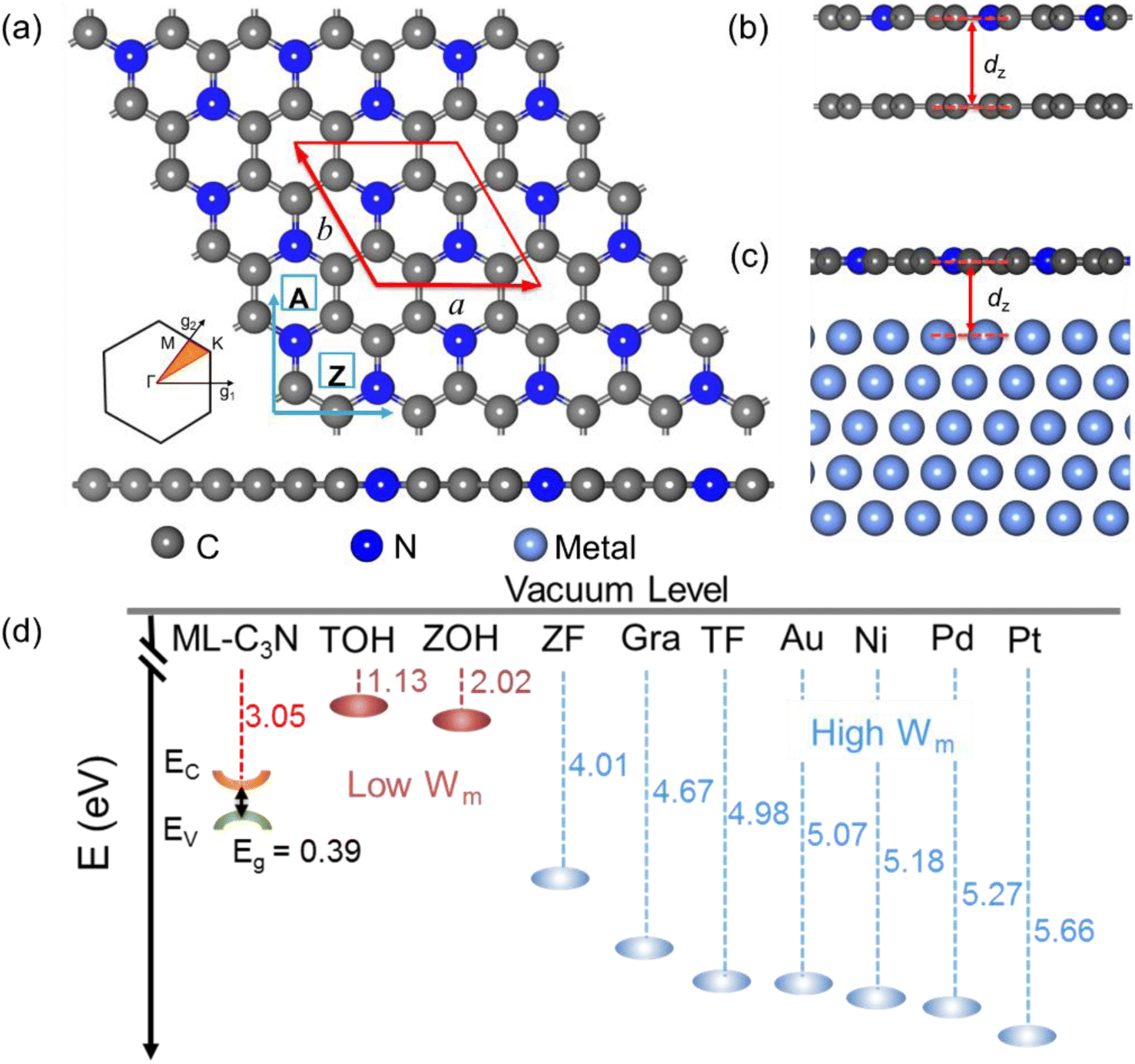 | ||
| Fig. 1 (a) Top and side views of the free-standing ML C3N. The red rhombus indicates the unit cell of the ML C3N (defined by a and b), and the arrows A and Z represent the armchair and zigzag directions of transport, respectively. The lower left panel plots the Brillouin zone associated with the two lattices. (b) Side view of the ML C3N contact with 2D metals (the 2D graphene as an example) and (c) bulk metals. (d) Computed band alignments between the ML C3N and work functions of metals (Wm). EC, EV, and Eg represent the conduction band edge, valence band edge, and band gap of the ML C3N, respectively. The TOH, ZOH, ZF, Gra, and TF stand for Ti2C(OH)2, Zr2C(OH)2, Zr2CF2, graphene, and Ti2CF2, respectively. | ||
The two-probe ML C3N-based FET model established to investigate the contact barriers of ML C3N FETs is shown in Fig. 6(a). The optimized ML C3N–metal contacts are distributed in the left and right semi-infinite-length electrode regions. Meanwhile, the pristine ML C3N was used as the channel, and the channel length was 5–6 nm. Carrier injection in ML C3N-based FETs involves two interfaces: the interface B between the metal electrode A and the bottom ML C3N region C and the interface D between the source/drain region and channel region E. Because of the anisotropy of ML C3N, we further assessed the transport properties of ML C3N FETs along the zigzag direction and armchair direction.
2.2. Computational methods
The Vienna ab initio simulation package (VASP) code was applied to determine the geometrical optimizations and electronic properties of ML C3N–metal contact systems based on the density functional theory (DFT).57–59 The interaction between ions and electrons is described using projected augmented wave (PAW) approximation.60 The exchange–correlation interactions are described by generalized gradient approximation (GGA) with the Perdew–Burke–Ernzerhof (PBE).61 We set 500 eV as the cut-off energy when using the plane-wave basis set. By using Grimm's zero damping DFT-D3 approach, vdW correction was processed.62 During geometry optimization, the convergence threshold for the residual force was at least 0.001 eV Å−1, and the energy difference was converged to less than 1 × 10⁻⁵ eV per atom. The Monkhorst–Pack k-point grid was sampled in the Brillouin zone with a separation of 0.02 Å−1.63 The vacuum region was set to no less than 15 Å to avoid interaction between adjacent slabs.The ML C3N FET simulations were performed by using DFT and the nonequilibrium Green's function (NEGF) method in the Quantum Atomistix Tool Kit (Quantum ATK) 2019 package.64,65 The double-ζ polarization (DZP) form takes into account the linear combination of atomic orbits (LCAO) basis set. The cut-off energy for the real space was set to 125 eV. The transmission coefficient T(ky, E) was calculated by using the following formula:
| T(ky, E) = Tr[ΓL(ky, E)G(ky, E)ΓR(ky, E)G+(ky, E)] |
3. Results and discussions
3.1. Atomic structure and binding behavior of the ML C3N–metal interfaces
The atomic structure of ML C3N is illustrated in Fig. 1(a). ML C3N possesses P/6mmm symmetry with a planar hexagonal structure. The planar lattice constants of ML C3N obtained by PBE-vdW functional optimization are a = 4.86 Å and b = 4.21 Å, which are in agreement with the previous theoretical results.73,74 Fig. 2 displays the optimized atomic structure of the ML C3N–metal interfaces. The relaxed structure of ML C3N on each metal surface is well-maintained and similar to the initial structure. The equilibrium interface distance (dz) and the binding energy (Eb) were combined to analyze the binding level between ML C3N and the metals. As shown in Fig. 1(b), dz is defined as the average distance from the interface between the topmost layer of metal atoms and the neighboring ML C3N layer in the vertical direction. To further explore the binding characteristics at the metal–ML C3N interfaces, the binding energy Eb was calculated by Eb = (EC3N + EM − Esys)/n, where EC3N, EM, and Esys represent the relaxed energies of isolated C3N, the free-standing metal surfaces, and the combined system, respectively, and n is the total number of C and N atoms in a C3N supercell. For Zr2C(OH)2, Ti2C(OH)2, Zr2CF2, Ti2CF2, Pt, Pd, Au, Ni, and graphene, the dz values from ML C3N were 2.17, 2.26, 2.94, 2.95, 3.18, 3.22, 3.39, 3.41, and 3.47 Å, respectively, which is consistent with the approximate distance values of their vdW interaction.35 Because of the large distance between ML C3N and metals at the interfaces, there was no direct wave function overlap. The sum of the covalent radii of the C atom and the metal atom in the weak bond was much larger than the vertical distance between the layers, indicating that ML C3N and metals are connected by vdW stacking. The atomic structures of the monolayer C3N/metal interfaces were well-retained after optimization, as shown in Fig. 2, indicating the good stability of the interfaces. According to previous reports, we used the binding energies of the interfaces to further study their stability.21,34,42,45 The binding energies Eb of the ML C3N/metal interfaces were in the range of 0.04–0.14 eV, thus suggesting that weak vdW interactions are established between ML C3N and metals to prevent chemical disturbances and maintain structural stability, which further demonstrates the good stability of the interfaces (Table 1).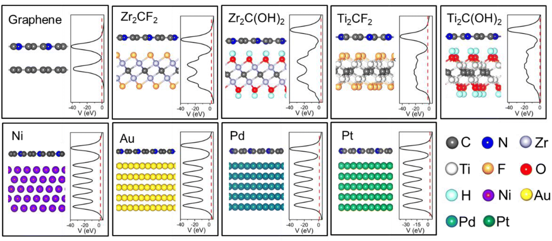 | ||
| Fig. 2 Optimized side-views and the average electrostatic potential distribution in the planes normal to the interfaces of the ML C3N on graphene, Zr2CF2, Zr2C(OH)2, Ti2CF2, Ti2C(OH)2, Ni, Au, Pd, and Pt surfaces. The Fermi level is represented by red dashed lines. | ||
![[small epsilon, Greek, macron]](https://www.rsc.org/images/entities/i_char_e0c6.gif) is the average absolute ML C3N surface lattice constant mismatch. The equilibrium distance dz is the average distance between the ML C3N–metal interfaces in the vertical direction. The binding energy Eb is the energy per ML C3N being removed from the metal surface. WM and WC-M are the calculated work function for clean metals surface and adsorbed the ML C3N–metal system, respectively. Φe,A/ZL(Φh,A/ZL) is the transport SBH of the electron (hole) along the armchair/zigzag direction in the lateral interface by LDDOS calculation. EA/Zg is the transport gap by the LDDOS calculation along zigzag armchair orientation, defined as EA/Zg = Φe,A/ZL + Φh,A/ZL. ΔQ is the charge transfer from the metal to the ML C3N. LA/Zg is the channel length of the ML C3N FET. The calculated work function of the ML C3N is W = 3.05 eV
is the average absolute ML C3N surface lattice constant mismatch. The equilibrium distance dz is the average distance between the ML C3N–metal interfaces in the vertical direction. The binding energy Eb is the energy per ML C3N being removed from the metal surface. WM and WC-M are the calculated work function for clean metals surface and adsorbed the ML C3N–metal system, respectively. Φe,A/ZL(Φh,A/ZL) is the transport SBH of the electron (hole) along the armchair/zigzag direction in the lateral interface by LDDOS calculation. EA/Zg is the transport gap by the LDDOS calculation along zigzag armchair orientation, defined as EA/Zg = Φe,A/ZL + Φh,A/ZL. ΔQ is the charge transfer from the metal to the ML C3N. LA/Zg is the channel length of the ML C3N FET. The calculated work function of the ML C3N is W = 3.05 eV
| Graphene | Zr2CF2 | Ti2CF2 | Ti2C(OH)2 | Zr2C(OH)2 | Ni | Au | Pd | Pt | |
|---|---|---|---|---|---|---|---|---|---|
| (%) |
0.81 | 2.64 | 2.64 | 2.08 | 2.08 | 1.65 | 1.80 | 1.33 | 3.27 |
| dz (Å) | 3.47 | 2.94 | 2.95 | 2.26 | 2.17 | 3.41 | 3.39 | 3.22 | 3.18 |
| Eb (eV) | 0.04 | 0.05 | 0.06 | 0.08 | 0.09 | 0.10 | 0.10 | 0.10 | 0.14 |
| WC-M (eV) | 3.56 | 3.37 | 4.40 | 1.96 | 2.22 | 4.43 | 3.92 | 4.04 | 4.24 |
| WM (eV) | 4.67 | 4.01 | 4.98 | 1.13 | 2.02 | 5.18 | 5.07 | 5.27 | 5.66 |
| ΔQ (e Å−1) | −0.02 | −0.03 | −0.06 | 0.07 | 0.095 | −0.04 | −0.05 | −0.04 | −0.07 |
| Φe,ZL (eV) | 0.38 | 0.39 | 0.43 | −0.16 | −0.19 | 0.23 | 0.34 | 0.43 | 0.36 |
| Φh,ZL (eV) | 0.00 | −0.03 | −0.11 | 0.43 | 0.52 | 0.00 | 0.07 | 0.00 | 0.00 |
| EZg (eV) | 0.38 | 0.36 | 0.32 | 0.27 | 0.33 | 0.23 | 0.41 | 0.43 | 0.36 |
| Φe,AL (eV) | 0.38 | 0.42 | 0.36 | −0.17 | −0.24 | 0.35 | 0.49 | 0.42 | 0.39 |
| Φh,AL (eV) | 0.00 | −0.07 | −0.02 | 0.38 | 0.41 | −0.03 | −0.10 | 0.00 | 0.00 |
| EAg (eV) | 0.38 | 0.35 | 0.34 | 0.21 | 0.17 | 0.32 | 0.39 | 0.42 | 0.39 |
| LZg (Å) | 53 | 58 | 58 | 58 | 58 | 53 | 53 | 53 | 53 |
| LAg (Å) | 50 | 50 | 50 | 50 | 50 | 50 | 50 | 50 | 50 |
According to previous reports, 2D metals (such as graphene and MXenes) are capable of forming weak bonds with 2D semiconductors, while bulk metals (such as Au, Ni, and Pd) prefer to form strong bonds with 2D semiconductors.34,47,67,75 Compared with the other C-based 2D semiconductor ML C2N, ML C2N–Pd interface forms medium binding with Eb of 0.14 eV and dz of 2.55 Å, and the ML C2N–Al and Sc interfaces form strong binding with Eb of 0.22 eV and 0.78 eV, and dz of 1.80 Å and 1.71 Å, respectively. This indicates that ML C2N forms stronger interactions with metals than ML C3N.40
3.2. Electronic structure of the ML C3N–metal interfaces
Fig. 3 shows that ML C3N is a p-type semiconductor with an indirect bandgap of 0.39 eV, in which the valence band maximum (VBM) and the conduction band minimum (CBM) are located at the Γ point and the M point, respectively. This is exactly the same as the findings from previous theoretical calculations at the PBE level and experimental values.28,30,73 By fitting the CBM and VBM of ML C3N to parabolic functions, the effective masses of electrons and holes
  were calculated as
 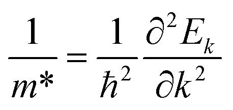 , where k is the wave vector and Ek is the energy corresponding to the wave vector k. According to the above formula, the calculated effective masses of ML C3N were 0.53 me for the electrons and 0.21 me for the holes in the armchair direction, 0.31 me for the electrons and 0.72 me for the holes in the zigzag direction, respectively (me is the effective mass of free electrons). The effective electron mass in the zigzag direction of ML C3N is almost two times smaller than that in the armchair direction, while the effective hole mass in the zigzag direction of ML C3N is around three times larger than that in the armchair direction. Therefore, the above results demonstrate that the effective masses of electrons and holes have obvious anisotropy. Meanwhile, these small effective masses promise large carrier mobility (the predicted hole mobility is 1.08 × 104 cm2 V−1 s−1 according to the literature),28 which fully embodies the superior electron transmission capability of ML C3N.
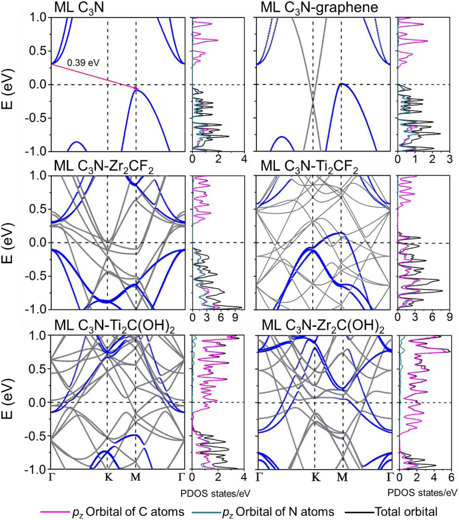 | ||
| Fig. 3 Band structures and PDOS of the pristine ML C3N and the ML C3N–graphene, Zr2CF2, Ti2CF2, Ti2C(OH)2, and Zr2C(OH)2 systems. Gray and blue lines are the band structure of the interfacial systems and the band structures of the interfacial systems projected to the ML C3N. The purple (green) and the black lines are the DOS of the pz orbital of C (N) atoms and the total orbital for the interfacial systems projected to the ML C3N, respectively. The Fermi level is set at zero energy and denoted by the lateral black dashed lines. | ||
The band structures of the ML C3N–metal systems are shown in the left part of Fig. 3 and 4. Except for the Pd and Pt electrodes, the inherent band structure of ML C3N was retained in the selected electrodes compared to the pristine ML C3N, even though in supercell computation band folding would be considered. The band gaps of ML C3N were 0.30, 0.32, 0.32, 0.35, 0.36, 0.37, and 0.39 eV in the ML C3N–graphene, –Zr2C(OH)2, –Ti2C(OH)2, –Ni, –Ti2CF2, –Au, and –Zr2CF2 systems, respectively, which are consistent with the 0.39 eV bandgap of isolated ML C3N. On the other hand, the bandgap of ML C3N disappeared and its band structure was significantly hybridized after contact with Pd and Pt metals. Due to electron transfer between ML C3N and the metals, the energy transfer of ML C3N was observed at the interfaces. The band energy of ML C3N moved down, and the CBM of ML C3N passed through the Fermi level after contact with Ti2C(OH)2 and Zr2C(OH)2, which indicates the formation of n-type contacts. Meanwhile, the band energy of ML C3N moved upward, and the VBM of ML C3N was closer to the Fermi level after contact with graphene, Ti2CF2, Zr2CF2, and all bulk metals, which indicates p-type contacts at these ML C3N–metal interfaces.
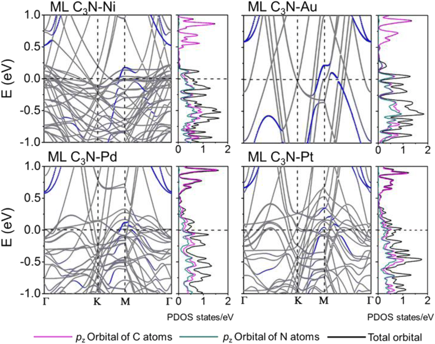 | ||
| Fig. 4 Band structures and PDOS of the pristine ML C3N–Ni, Au, Pd, and Pt systems. Gray and blue lines are the band structure of the interfacial systems and the band structures of the interfacial systems projected to the ML C3N. The purple (green) and the black lines are the DOS of the pz orbital of C (N) atoms and the total orbital for the interfacial systems projected to the ML C3N, respectively. The Fermi level is set at zero energy and denoted by the lateral black dashed lines. | ||
The interaction at the ML C3N–metal interfaces was further analyzed by evaluating their density of states (DOS) in the interfacial systems, as shown in the right part of Fig. 3 and 4. In Fig. S1,† the DOS of pristine ML C3N near the CBM is primarily composed of the pz orbitals of C atoms, while that near the VBM is primarily composed of the pz orbitals of C atoms and N atoms. Similarly, the orbital contribution of ML C3N in the composite systems was almost consistent with that in pristine ML C3N. The band gap of ML C3N was maintained well even after coming in contact with Zr2C(OH)2, Ti2C(OH)2, Ti2CF2, Zr2CF2, graphene, Ni, and Au metals due to weak vdW bonding. In addition, a small electronic state appeared in the DOS of ML C3N after coming in contact with Pt and Pd metals, indicating the absence of bandgap and hybridization of the orbitals. Therefore, the contact types of ML C3N with metals obtained from the PDOS are the same as those inferred from the band structure.
To further explore electronic transfer at the ML C3N–metal interfaces, we calculated the plane-averaged charge density difference along the vertical z-direction to better see the gain and loss of interface charge, as shown in Fig. 5. The charge density difference Δρ is defined by the following equation.
| Δρ = ρA − ρM − ρC3N |
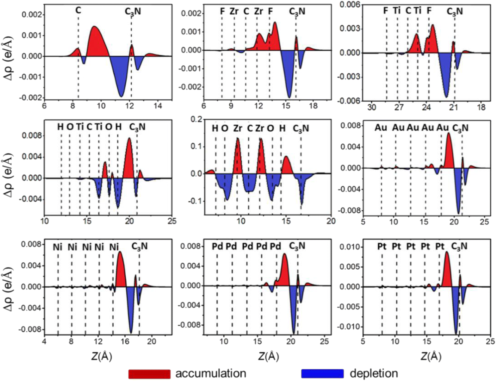 | ||
| Fig. 5 Plane-averaged charge difference along the vertical z-direction to the metals–ML C3N interfaces. The red (blue) region represents charge accumulation (depletion) regions. | ||
3.3. Barriers in the ML C3N FETs
To further investigate the barriers in the contact systems, we constructed a two-probe FET model based on ML C3N with a 5–6 nm channel length along the armchair and zigzag directions, as described in Fig. 6(a). Two different types of interfaces are encountered by carriers transferred from an electrode to a channel. The interface between ML C3N and the metal on the electrode in the vertical direction is labelled as interface B, while the other interface between the ML C3N–metal complexes and the ML C3N channel in the lateral direction is labelled as interface D. Tunneling barriers may appear due to the existence of the vdW gap at interface B, and Schottky barriers may appear at interfaces B and D. In Fig. 2, the tunneling barrier is viewed as an effective potential above the Fermi level at the ML C3N–metal contacts. In the systems under consideration, because the effective potentials at all interfaces are below the Fermi level, there is no tunneling barrier at the interfaces with a tunneling probability of 100%.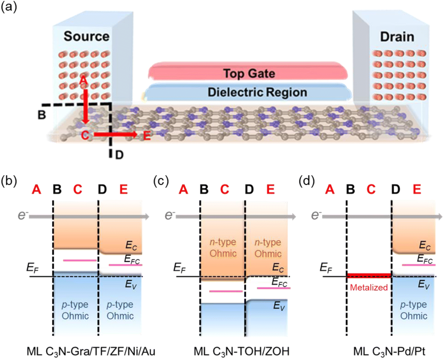 | ||
| Fig. 6 (a) Schematic diagram of the ML C3N FET. The carrier paths are marked by red arrows. A, C, and E represent three regions, and black dashed lines B and D represent two interfaces in the ML C3N FET, i.e., vertical interface B and lateral interface D. (b–d) Three possible band diagrams in terms of the quantum transport calculations of ML C3N FETs with graphene, Ti2C(OH/F)2, Zr2C(OH/F)2, Au, Ni, Pd, and Pt electrodes. EC and EV are the conduction and valence band edges of the ML C3N, respectively. EF and EFC denote the Fermi level of the ML C3N-electrode junctions and the band gap center of the channel ML C3N, respectively. The TOH, ZOH, ZF, Gra, and TF stand for Ti2C(OH)2, Zr2C(OH)2, Zr2CF2, graphene, and Ti2CF2, respectively. | ||
SBH is an essential parameter for evaluating the metal–semiconductor contact in the ML C3N FETs, and it is also a vital factor for determining carrier injection efficiency and resistance. The vertical Schottky barriers of the 2D semiconductor FETs at interface B can be obtained from the commonly used method, namely band structure calculations, wherein the electron/hole SBH is obtained by the observable CBM/VBM of the 2D semiconductor and the energy differences between the Fermi levels of the systems. From the band structure in Fig. 3, it can be inferred that the ML C3N–Zr2CF2 contact system forms a p-type Schottky contact, and the ML C3N–Zr2C(OH)2 and –Ti2C(OH)2 contact systems form n-type ohmic contacts with the Fermi level above the CBM of ML C3N, while the ML C3N–graphene, –Ti2CF2, –Ni, and –Au contact systems form p-type ohmic contacts with the Fermi level below the VBM of ML C3N. In particular, the band structure of ML C3N hybridizes when it comes in contact with Pd and Pt electrodes, allowing carriers to pass directly through the electrode to the underside of ML C3N without a vertical Schottky barrier.
To evaluate the more reliable vertical SBH of the 2D semiconductor FETs, quantum transport simulations were adopted by constructing a two-probe FET model.37 Using Pt, Pd, Ni, Au, Zr2C(OH)2, Ti2C(OH)2, Ti2CF2, Zr2CF2, and graphene electrodes, the local device density of states (LDDOS) of the ML C3N–metal systems projected into ML C3N under zero bias and zero gate voltage were estimated based on quantum transport simulations, as presented in Fig. 7 and 8. We further explored the transport properties at the ML C3N–metal interfaces based on FETs in the zigzag direction and armchair direction due to the anisotropy of ML C3N. The ML C3N–metal interfaces formed ohmic contacts and the same type of vertical contact in both directions. The bandgap of the ML C3N underneath the electrode was well-preserved in the ML C3N–graphene, –Zr2CF2, –Ti2CF2, –Ti2C(OH)2, and –Zr2C(OH)2 contact systems, of which p-type ohmic contacts were obtained with graphene, Zr2CF2, and Ti2CF2 electrodes, while n-type ohmic contacts were obtained with Ti2C(OH)2 and Zr2C(OH)2 electrodes. The electrode region of the ML C3N–graphene and –Zr2CF2 systems in the zigzag direction and the ML C3N–graphene, –Ti2CF2, and –Ti2C(OH)2 systems in the armchair direction had gap states, which can be regarded as metal-induced gap states (MIGS). On the other hand, the p-type vertical ohmic contacts are obtained due to the strong interaction between ML C3N and the bulk metals, and electronic states appeared in the bandgap of their electrode regions.
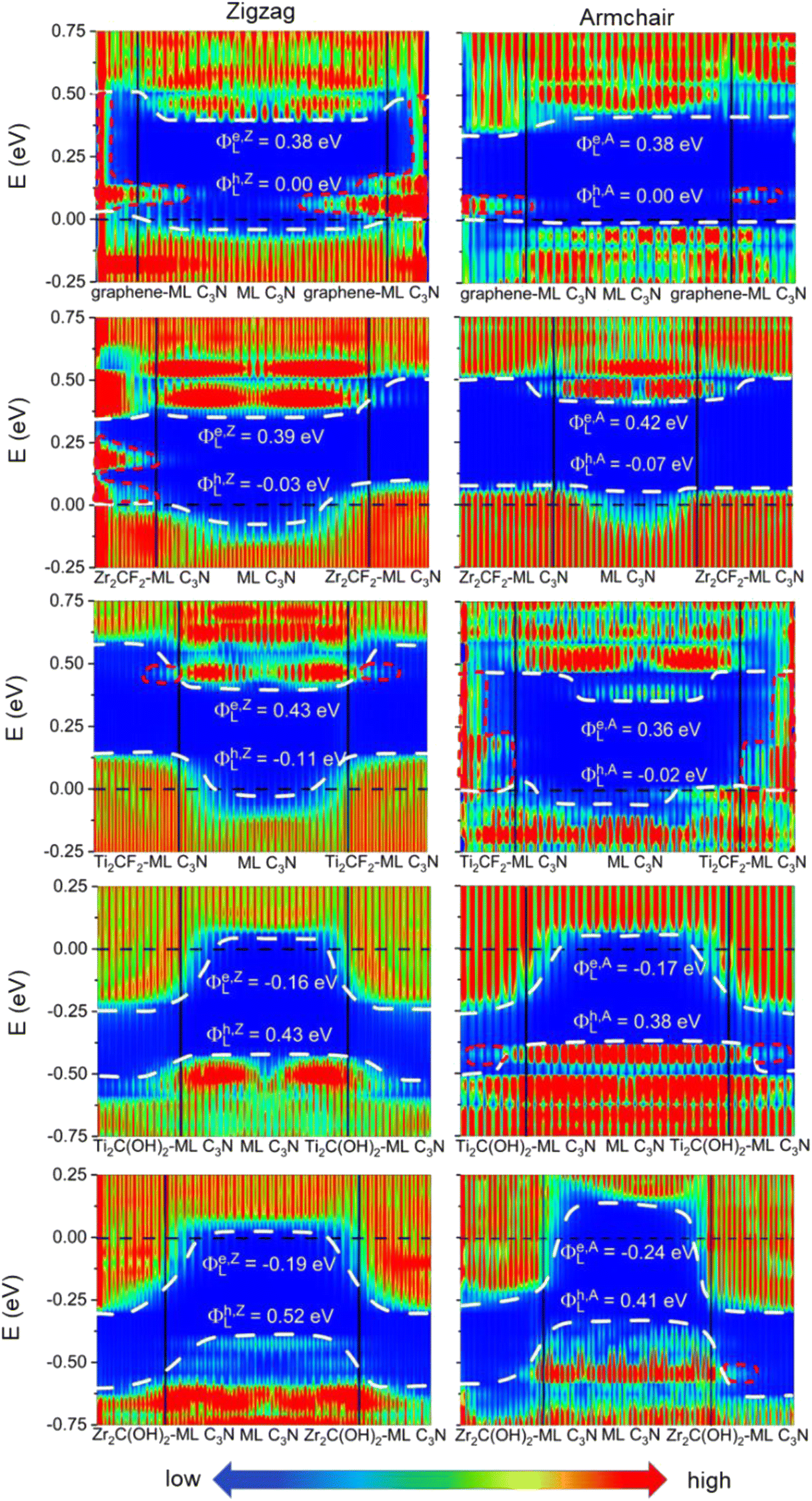 | ||
| Fig. 7 Zero-bias and zero-gate voltage LDDOS of the ML C3N FETs with graphene, Zr2CF2, Ti2CF2, Ti2C(OH)2, and Zr2C(OH)2 electrodes, and the channel lengths are L = 5–6 nm. The Fermi level is represented by the black dashed line. The white dashed lines represent the VBM and CBM of ML C3N. The interface states are represented by the red short dash lines. | ||
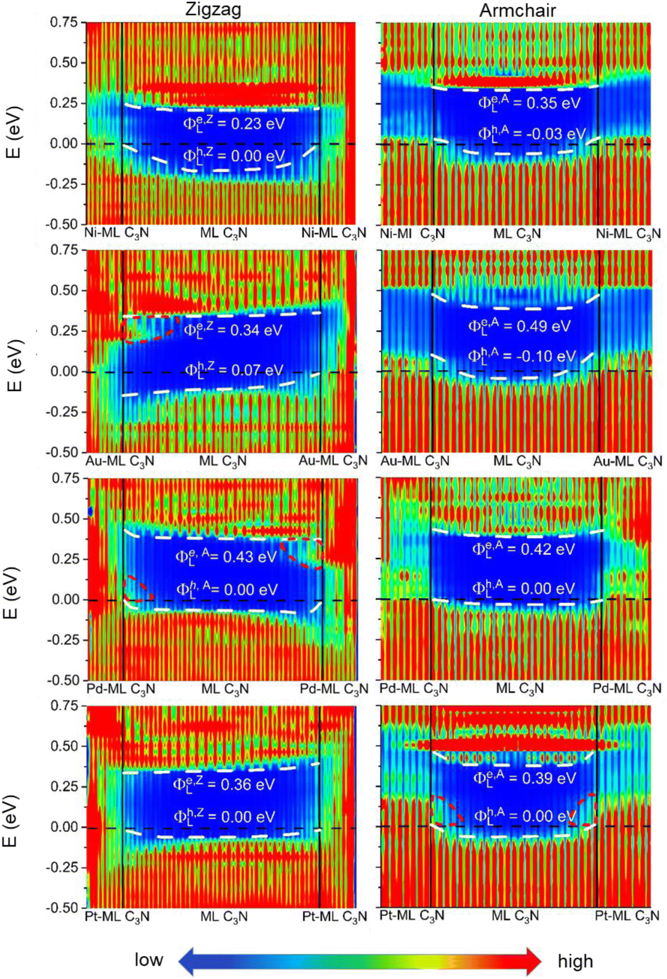 | ||
| Fig. 8 Zero-bias and zero-gate voltage LDDOS of the ML C3N FETs with Pt, Pd, Ni, and Au electrodes, and the channel lengths are L = 5–6 nm. The Fermi level is represented by the black dashed line. The white dashed lines represent the VBM and CBM of ML C3N. The interface states are represented by the red short dash lines. | ||
The vertical barriers estimated from the quantum transport simulation were not exactly the same as those from the band structure calculation. For the ML C3N-based FET with the Zr2CF2 electrode, a p-type Schottky contact was obtained as per band structure calculations, while a p-type ohmic contact was obtained by the quantum transport simulations. Additionally, p-type ohmic contacts were obtained by both the above methods for the ML C3N–Ni and –Au systems. However, the band structure of the systems was maintained well, and the Fermi level was lower than the VBM of ML C3N in the band structure calculations, while in the quantum transport simulations, the appearance of gap states leads to the hybridization of ML C3N and the metal electrodes. The main reason for the difference between these two methods is that the effect of the channels in ML C3N is ignored in the band structure calculations, while the electrode region and ML C3N channels are calculated as a whole in quantum transport simulations, and coupling between the two parts is also considered. Therefore, coupling between the electrode and the channel is crucial for evaluating the vertical SBHs of the ML C3N-based FETs and may also result in MIGS at the ML C3N–metal vertical interfaces.
Work function approximation is a typical method of assessing lateral Schottky barriers, in which the electrode and channel are regarded as separate parts.34,42 Therefore, this method ignores the coupling between the two parts. However, coupling between the electrode and channel is considered in quantum transport simulations because they are taken as a whole, which may lead to MIGS at the lateral interfaces and is crucial to studying lateral SBH. Previous studies using quantum transport simulation show that the lateral hole SBHs of trilayer/bilayer/ML black phosphorene systems are 0.20/0.19/0.26 eV, which are well in line with the experimental values of 0.21/0.23/0.35 eV.34,41,76,77 As a result, we employed quantum transport simulations to evaluate the lateral SBHs in the ML C3N–metal contact systems.
In the quantum transport simulations, the lateral electron/hole SBH Φe,A/ZL/Φh,A/ZL was determined from the energy differences between the Fermi level of the ML C3N–metal contacts and the CBM/VBM of the ML C3N channel at the interface D of the FETs:
| Φe,A/ZL = EC − EF and Φh,A/ZL = EF − EV |
3.4. Discussion
Based on quantum transport simulations, the tunnel barriers and Schottky barriers of the ML C3N–metal contacts can be classified into three types along the armchair direction, as shown in Fig. 6(b)–(d). In ML C3N FETs with graphene, Ti2CF2, Zr2CF2, Ni, and Au electrodes, the bandgap is preserved in both the electrode and channel regions, and the Fermi level lowers the VBM of ML C3N, forming p-type ohmic contacts at both interfaces B and D, as depicted in Fig. 6(b). Moreover, in ML C3N FETs with Ti2C(OH)2 and Zr2C(OH)2 electrodes, n-type ohmic contacts are formed at both interfaces as the Fermi level is above the CBM of ML C3N, and the band gap is equally maintained in both electrode and channel regions, as depicted in Fig. 6(c). In ML C3N FETs with Pd and Pt electrodes, the strong interaction between ML C3N and the electrodes causes electronic states to arise in the bandgap of the electrode region, resulting in significant metallization of the interface B, and a p-type ohmic contact is also observed at the interface D for the same reason, as shown in Fig. 6(d). Due to the isotropic interfacial properties of the ML C3N FETs, the ML C3N–metal systems have the same contact type in both the zigzag and armchair directions, except for the ML C3N–Au contact system, which forms a p-type quasi-ohmic contact because its Fermi level is remarkably close to the VBM of ML C3N, as shown in Fig. S2.† All three types of ML C3N–metal contact systems mentioned above can form ohmic contacts at interfaces B and D, which can facilitate electron injection and electron transport to the ML C3N channel.Remarkably, the presence of interface gap states and electronic transmission may cause the Fermi energy to be fixed at a special level, making it challenging to experimentally adjust the Schottky barriers to achieve ideal ohmic contacts. To quantitatively analyze the degree of FLP limitations, the Schottky barrier pinning factor S was obtained as S = |dΦL/dWm|, where ΦL represents the lateral Schottky barrier of the contact system, and Wm is the work function of the metal. If the slope of the linear dependence data is close to 1, there is no FLP according to the Schottky–Moore rule, whereas, a slope close to 0 indicates complete FLP. As illustrated in Fig. 9(a), since the Schottky barriers of the ML C3N–metal interfaces do not exhibit significant anisotropy, the zigzag direction was chosen to study the FLP effect. The lateral hole SBH demonstrated linear dependence on the work function with a pinning factor of −0.13, which is close to 0, indicating strong FLP. The Fermi level of ML C3N in the ML C3N FETs is fixed above the CBM or under the VBM, as presented in Fig. 9(b), while the Fermi level of some other 2D semiconductors is pinned in the gap states.78–81 Thus, strong FLP results in the formation of ohmic contacts in the C3N FETs rather than Schottky contacts, unlike in other 2D semiconductors FETs. This is mainly due to the narrow band gap (0.39 eV) of ML C3N and the inherent properties of the ML C3N–metal contact systems.
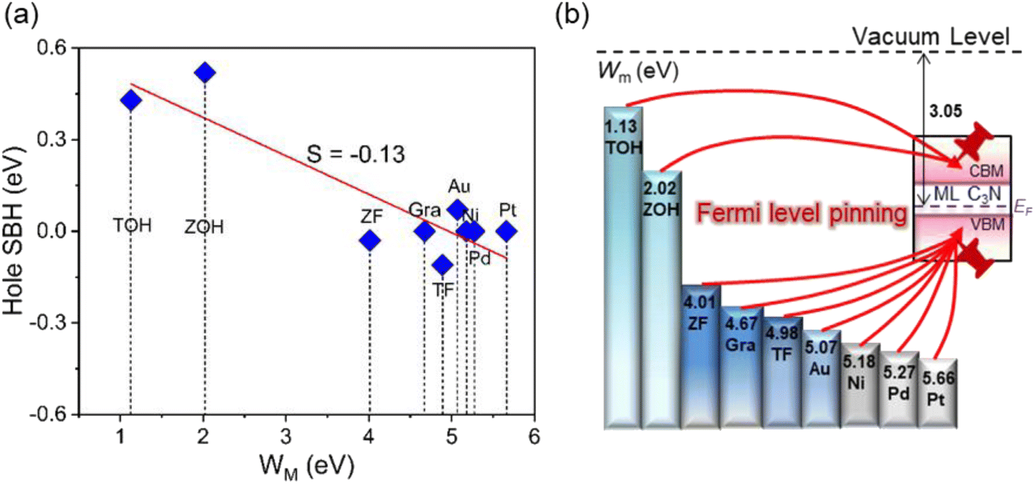 | ||
| Fig. 9 (a) Lateral hole SBH of the metal–ML C3N systems versus the work function values of metals. The slope presents the FLP strength. (b) Schematic plot of the FLP for ML C3N FETs. The TOH, ZOH, ZF, Gra, and TF stand for Ti2C(OH)2, Zr2C(OH)2, Zr2CF2, graphene, and Ti2CF2, respectively. | ||
The ideal ohmic contacts are realized with the 2D MXenes of TiC and ZrC with F and OH functional groups, and the different functional groups can modulate the type of ohmic contacts, i.e., the carrier polarity of the transistors can shift from n-type with OH functional group to p-type with F functional group. This is mainly because 2D MXenes with the OH functional group have a small work function, while 2D MXenes with the F functional group have a large work function. Thus, 2D MXenes are ideal electrodes for forming ohmic contacts in ML C3N FETs, and an appropriate functional group can be selected to change the contact type in these systems.
4. Conclusion
In this work, the contact properties of ML C3N FETs with various 2D metal electrodes (graphene, Ti2C(OH/F)2, and Zr2C(OH/F)2) and bulk metals (Au, Ni, Pd, and Pt) are comprehensively explored by employing ab initio electronic structure calculations and quantum transport simulations. Vertical ohmic contacts are formed with both 2D and bulk metal electrodes in ML C3N FETs except for Zr2CF2. Meanwhile, isotropic properties are observed in terms of the type and height of the lateral Schottky barriers along the zigzag and armchair directions. In ML C3N-based FETs, n-type lateral ohmic contacts are formed with Ti2C(OH)2 and Zr2C(OH)2 metals, while p-type lateral ohmic or quasi-ohmic contacts are formed with graphene, Ti2CF2, Zr2CF2, Au, Ni, Pd, and Pt metals. Conspicuously, the type of ohmic contact with the 2D MXene electrodes can be tuned by modulating their functional groups. A strong FLP effect (pinning factor of −0.13) is present at the Fermi levels pinned above the CBM and under the VBM of ML C3N, which is beneficial for the formation of ohmic contacts. This study not only offers a theoretical basis for the interfacial properties of ML C3N FETs with different electrodes but also guides the design of ML C3N FETs that form ohmic contacts.Conflicts of interest
There are no conflicts to declare.Acknowledgements
This work is supported by the National Natural Science Foundation of China (No. 11904409 and 51572296), Youth Innovation Technology Project of Higher School in Shandong Province (2022KJ139), Postdoctoral Research Foundation of China (No. 2018M642721), and Shandong Postdoctoral Funded Project (201901012).References
- Y. Liu, X. Duan, Y. Huang and X. Duan, Chem. Soc. Rev., 2018, 47, 6388–6409 RSC.
- R. Quhe, L. Xu, S. Liu, C. Yang, Y. Wang, H. Li, J. Yang, Q. Li, B. Shi, Y. Li, Y. Pan, X. Sun, J. Li, M. Weng, H. Zhang, Y. Guo, L. Xu, H. Tang, J. Dong, J. Yang, Z. Zhang, M. Lei, F. Pan and J. Lu, Phys. Rep., 2021, 938, 1–72 CrossRef CAS.
- Y. Pan, J. Phys. Chem. Solids, 2023, 174, 111152 CrossRef CAS.
- Y. Pan, S. Chen, P. Wang, Y. Li and Q. Zheng, Ceram. Int., 2019, 45, 19534–19537 CrossRef CAS.
- Y. Pan and W. M. Guan, Int. J. Hydrogen Energy, 2019, 44, 10407–10414 CrossRef CAS.
- Y. Pan, Mater. Sci. Eng., C, 2022, 281, 115746 CrossRef CAS.
- Y. Pan, J. Electron. Mater., 2019, 48, 5154–5160 CrossRef CAS.
- F. Schwierz, Nat. Nanotechnol., 2010, 5, 487–496 CrossRef CAS PubMed.
- K. Kim, J. Y. Choi, T. Kim, S. H. Cho and H. J. Chung, Nature, 2011, 479, 338–344 CrossRef CAS PubMed.
- S. Cahangirov, M. Topsakal, E. Akturk, H. Sahin and S. Ciraci, Phys. Rev. Lett., 2009, 102, 236804 CrossRef CAS PubMed.
- P. Vogt, P. De Padova, C. Quaresima, J. Avila, E. Frantzeskakis, M. C. Asensio, A. Resta, B. Ealet and G. Le Lay, Phys. Rev. Lett., 2012, 108, 155501 CrossRef PubMed.
- E. Bianco, S. Butler, S. Jiang, O. D. Restrepo, W. Wind and J. E. Goldberger, ACS Nano, 2013, 5, 4412–4421 Search PubMed.
- L. Xie, M. Liao, S. Wang, H. Yu, L. Du, J. Tang, J. Zhao, J. Zhang, P. Chen, X. Lu, G. Wang, G. Xie, R. Yang, D. Shi and G. Zhang, Adv. Mater., 2017, 29, 1702522 CrossRef PubMed.
- S. B. M. Desai, S. R. Madhvapathy, A. B. Sachid, J. P. Llinas, Q. Wang, G. H. Ahn, G. Pitner, M. J. Kim, J. Bokor, C. Hu and H. S. P. Wong, Science, 2016, 354, 99 CrossRef CAS PubMed.
- J. Kang, W. Liu, D. Sarkar, D. Jena and K. Banerjee, Phys. Rev. X, 2014, 4, 031005 CAS.
- T. D. Ngo, T. Huynh, H. Jung, F. Ali, J. Jeon, M. S. Choi and W. J. Yoo, Adv. Sci., 2023, 10, e2301400 CrossRef PubMed.
- L. Li, Y. Yu, G. J. Ye, Q. Ge, X. Ou, H. Wu, D. Feng, X. H. Chen and Y. Zhang, Nat. Nanotechnol., 2014, 9, 372–377 CrossRef CAS PubMed.
- A. Bafekry, D. Gogova, M. M. Fadlallah, N. V. Chuong, M. Ghergherehchi, M. Faraji, S. A. H. Feghhi and M. Oskoeian, Phys. Chem. Chem. Phys., 2021, 23, 4865–4873 RSC.
- M. Xu, T. Liang, M. Shi and H. Chen, Chem. Rev., 2013, 113, 3766–3798 CrossRef CAS PubMed.
- W. Wei, S. Yang, G. Wang, T. Zhang, W. Pan, Z. Cai, Y. Yang, L. Zheng, P. He, L. Wang, A. Baktash, Q. Zhang, L. Liu, Y. Wang, G. Ding, Z. Kang, B. I. Yakobson, D. J. Searles and Q. Yuan, Nat. Electron., 2021, 4, 486–494 CrossRef CAS.
- Z. Chen, X. Li and J. Yang, Adv. Theory Simul., 2019, 2, 1800161 CrossRef.
- J. Mahmood, E. K. Lee, M. Jung, D. Shin, I. Y. Jeon, S. M. Jung, H. J. Choi, J. M. Seo, S. Y. Bae, S. D. Sohn, N. Park, J. H. Oh, H. J. Shin and J. B. Baek, Nat. Commun., 2015, 6, 6486 CrossRef CAS PubMed.
- W. Liu, J. Wang, X. Zheng, K. Zhang and X. Liu, Phys. Chem. Chem. Phys., 2022, 24, 29601–29608 RSC.
- M. Amiri, F. Bagherpour and H. Hadipour, Phys. Rev. Mater., 2022, 6, 094004 CrossRef CAS.
- K. Ma, Y. Wang, Y. Zheng, J. Xiao, L. Xu, X. Dai and Z. Wang, Adv. Theory Simul., 2022, 6, 2200611 CrossRef.
- Z. Tang, G. J. Cruz, Y. Wu, W. Xia, F. Jia, W. Zhang and P. Zhang, Phys. Rev. A, 2022, 17, 034068 CAS.
- D. Wang, Y. Bao, T. Wu, S. Gan, D. Han and L. Niu, Carbon, 2018, 134, 22–28 CrossRef CAS.
- X. Wang, Q. Li, H. Wang, Y. Gao, J. Hou and J. Shao, Phys. B, 2018, 537, 314–319 CrossRef CAS.
- L. Zhou, S. Yang, G. Ding, J.-Q. Yang, Y. Ren, S.-R. Zhang, J.-Y. Mao, Y. Yang, Y. Zhou and S.-T. Han, Nano Energy, 2019, 58, 293–303 CrossRef CAS.
- S. Yang, W. Li, C. Ye, G. Wang, H. Tian, C. Zhu, P. He, G. Ding, X. Xie, Y. Liu, Y. Lifshitz, S. T. Lee, Z. Kang and M. Jiang, Adv. Mater., 2017, 29, 1605625 CrossRef PubMed.
- J. Xu, J. Mahmood, Y. Dou, S. Dou, F. Li, L. Dai and J. B. Baek, Adv. Mater., 2017, 29, 1702007 CrossRef PubMed.
- G. Qin, J. Lin, H. Wang, J. Hu, Z. Qin and M. Hu, J. Mater. Chem. C, 2022, 10, 12080–12090 RSC.
- W. Y. Jiao, R. Hu, S. H. Han, Y. F. Luo, H. M. Yuan, M. K. Li and H. J. Liu, Nanotechnology, 2021, 33, 045401 CrossRef PubMed.
- Y. Pan, Y. Wang, M. Ye, R. Quhe, H. Zhong, Z. Song, X. Peng, D. Yu, J. Yang, J. Shi and J. Lu, Chem. Mater., 2016, 28, 2100–2109 CrossRef CAS.
- A. Allain, J. Kang, K. Banerjee and A. Kis, Nat. Mater., 2015, 14, 1195–1205 CrossRef CAS PubMed.
- K. Zhong, J. Li, G. Xu, Y. Yang, J.-M. Zhang and Z. Huang, J. Appl. Phys., 2021, 130, 124305 CrossRef CAS.
- Y. Wang, S. Liu, Q. Li, R. Quhe, C. Yang, Y. Guo, X. Zhang, Y. Pan, J. Li, H. Zhang, L. Xu, B. Shi, H. Tang, Y. Li, J. Yang, Z. Zhang, L. Xiao, F. Pan and J. Lu, Rep. Prog. Phys., 2021, 84, 056501 CrossRef CAS PubMed.
- X. He, W. Z. Li, Z. Gao, Z. H. Zhang and Y. He, J. Mater. Chem. C, 2023, 11, 4728–4741 RSC.
- M. M. Dong, G. P. Zhang, Z. L. Li, M. L. Wang, C. K. Wang and X. X. Fu, Phys. Chem. Chem. Phys., 2020, 22, 28074–28085 RSC.
- Z. Chen, R. Zhang and J. Yang, Langmuir, 2018, 34, 2647–2653 CrossRef CAS PubMed.
- Y. Pan, Y. Dan, Y. Wang, M. Ye, H. Zhang, R. Quhe, X. Zhang, J. Li, W. Guo, L. Yang and J. Lu, ACS Appl. Mater. Interfaces, 2017, 9, 12694–12705 CrossRef CAS PubMed.
- Y. Shu, Y. Liu, Z. Cui, R. Xiong, Y. Zhang, C. Xu, J. Zheng, C. Wen, B. Wu and B. Sa, Adv. Electron. Mater., 2023, 9, 2201056 CrossRef CAS.
- Q. Peng, C. Si, J. Zhou and Z. Sun, Appl. Surf. Sci., 2019, 480, 199–204 CrossRef CAS.
- G. Iannaccone, F. Bonaccorso, L. Colombo and G. Fiori, Nat. Nanotechnol., 2018, 13, 183–191 CrossRef CAS PubMed.
- T. Shen, J. C. Ren, X. Liu, S. Li and W. Liu, J. Am. Chem. Soc., 2019, 141, 3110–3115 CrossRef CAS PubMed.
- D. Çakır and F. M. Peeters, Phys. Rev. B: Condens. Matter Mater. Phys., 2014, 89, 245403 CrossRef.
- H. Zhong, R. Quhe, Y. Wang, Z. Ni, M. Ye, Z. Song, Y. Pan, J. Yang, L. Yang, M. Lei, J. Shi and J. Lu, Sci. Rep., 2016, 6, 21786 CrossRef CAS PubMed.
- C. Gong, L. Colombo, R. M. Wallace and K. Cho, Nano Lett., 2014, 14, 1714–1720 CrossRef CAS PubMed.
- X. Liu, M. S. Choi, E. Hwang, W. J. Yoo and J. Sun, Adv. Mater., 2022, 34, e2108425 CrossRef PubMed.
- L. Kong, R. Wu, Y. Chen, Y. Huangfu, L. Liu, W. Li, D. Lu, Q. Tao, W. Song, W. Li, Z. Lu, X. Liu, Y. Li, Z. Li, W. Tong, S. Ding, S. Liu, L. Ma, L. Ren, Y. Wang, L. Liao, X. Duan and Y. Liu, Nat. Commun., 2023, 14, 1014 CrossRef CAS PubMed.
- J. Kim, D. Rhee, M. Jung, G. J. Cheon, K. Kim, J. H. Kim, J. Y. Park, J. Yoon, D. U. Lim, J. H. Cho, I. S. Kim, D. Son, D. Jariwala and J. Kang, ACS Nano, 2023, 1073–1083 CAS.
- A. Grillo, A. Di Bartolomeo, F. Urban, M. Passacantando, J. M. Caridad, J. Sun and L. Camilli, ACS Appl. Mater. Interfaces, 2020, 12, 12998–13004 CrossRef CAS PubMed.
- Y. Liu, H. Xiao and W. A. Goddard 3rd, J. Am. Chem. Soc., 2016, 138, 15853–15856 CrossRef CAS PubMed.
- C. Wang, X. Xu, S. Tyagi, P. C. Rout, U. Schwingenschlogl, B. Sarkar, V. Khandelwal, X. Liu, L. Gao, M. N. Hedhili, H. N. Alshareef and X. Li, Adv. Mater., 2023, 35, e2211738 CrossRef PubMed.
- B. Lyu, M. Kim, H. Jing, J. Kang, C. Qian, S. Lee and J. H. Cho, ACS Nano, 2019, 13, 11392–11400 CrossRef CAS PubMed.
- J. Yan, D. Cao, M. Li, Q. Luo, X. Chen, L. Su and H. Shu, Small, 2023, 19, e2303675 CrossRef PubMed.
- G. F. Kresse and J. Furthmiiller, Phys. Rev. B: Condens. Matter Mater. Phys., 1996, 54, 11169–11186 CrossRef CAS PubMed.
- G. F. Kresse and J. Furthmiiller, Comput. Mater. Sci., 1996, 6, 15–50 CrossRef CAS.
- G. Kresse and J. Hafner, Phys. Rev. B: Condens. Matter Mater. Phys., 1993, 47, 558–561 CrossRef CAS PubMed.
- G. Kresse and D. Joubert, Phys. Rev. B: Condens. Matter Mater. Phys., 1999, 59, 1758–1775 CrossRef CAS.
- J. P. Perdew, K. Burke and M. Ernzerhof, Phys. Rev. Lett., 1996, 77, 3865–3868 CrossRef CAS PubMed.
- J. Klimes, D. R. Bowler and A. Michaelides, J. Phys.: Condens. Matter, 2010, 22, 022201 CrossRef PubMed.
- H. J. Monkhorst and J. D. Pack, Phys. Rev. B: Solid State, 1976, 13, 5188–5192 CrossRef.
- J. Taylor, H. Guo and J. Wang, Phys. Rev. B: Condens. Matter Mater. Phys., 2001, 63, 245407 CrossRef.
- M. Brandbyge, J.-L. Mozos, P. Ordejón, J. Taylor and K. Stokbro, Phys. Rev. B: Condens. Matter Mater. Phys., 2002, 65, 165401 CrossRef.
- A. H. D. Cheng and D. T. Cheng, Eng. Anal. Bound. Elem., 2005, 29, 268–302 CrossRef.
- Y. Pan, J. Dai, Z. Liu, M. Wu, H. Hu and J. Lu, J. Mater. Sci., 2020, 55, 11439–11450 CrossRef CAS.
- Y. Guo, G. Zhao, F. Pan, R. Quhe and J. Lu, J. Electron. Mater., 2022, 51, 4824–4835 CrossRef CAS.
- H. Li, Y. Liu, Z. Bai, J. Xiong, F. Liu, G. Zhou, T. Qing, S. Zhang and J. Lu, Phys. Lett. A, 2022, 433, 128029 CrossRef CAS.
- S. Liu, J. Li, B. Shi, X. Zhang, Y. Pan, M. Ye, R. Quhe, Y. Wang, H. Zhang, J. Yan, L. Xu, Y. Guo, F. Pan and J. Lu, J. Mater. Chem. C, 2018, 6, 5651–5661 RSC.
- Y. Liang and L. Yang, Phys. Rev. Lett., 2015, 114, 063001 CrossRef CAS PubMed.
- Y. Zhang, T. R. Chang, B. Zhou, Y. T. Cui, H. Yan, Z. Liu, F. Schmitt, J. Lee, R. Moore, Y. Chen, H. Lin, H. T. Jeng, S. K. Mo, Z. Hussain, A. Bansil and Z. X. Shen, Nat. Nanotechnol., 2014, 9, 111–115 CrossRef CAS PubMed.
- A. Bafekry, S. Farjami Shayesteh and F. M. Peeters, Phys. Chem. Chem. Phys., 2019, 21, 21070–21083 RSC.
- J. Mahmood, E. K. Lee, M. Jung, D. Shin, H. J. Choi, J. M. Seo, S. M. Jung, D. Kim, F. Li, M. S. Lah, N. Park, H. J. Shin, J. H. Oh and J. B. Baek, Proc. Natl. Acad. Sci. U. S. A., 2016, 113, 7414–7419 CrossRef CAS PubMed.
- D. S. Gavali, Y. Kawazoe and R. Thapa, J. Colloid Interface Sci., 2022, 610, 80–88 CrossRef CAS PubMed.
- S. Das, W. Zhang, M. Demarteau, A. Hoffmann, M. Dubey and A. Roelofs, Nano Lett., 2014, 14, 5733–5739 CrossRef CAS PubMed.
- X. Zhang, Y. Pan, M. Ye, R. Quhe, Y. Wang, Y. Guo, H. Zhang, Y. Dan, Z. Song, J. Li, J. Yang, W. Guo and J. Lu, Nano Res., 2017, 11, 707–721 CrossRef.
- C. Kim, I. Moon, D. Lee, M. S. Choi, F. Ahmed, S. Nam, Y. Cho, H.-J. Shin, S. Park and W. J. Yoo, ACS Nano, 2017, 11, 1588–1596 CrossRef CAS PubMed.
- J. Li, X. Sun, C. Xu, X. Zhang, Y. Pan, M. Ye, Z. Song, R. Quhe, Y. Wang, H. Zhang, Y. Guo, J. Yang, F. Pan and J. Lu, Nano Res., 2018, 11, 1834–1849 CrossRef CAS.
- H. Zhang, J. Xiong, M. Ye, J. Li, X. Zhang, R. Quhe, Z. Song, J. Yang, Q. Zhang, B. Shi, J. Yan, W. Guo, J. Robertson, Y. Wang, F. Pan and J. Lu, Phys. Rev. Appl., 2019, 11, 064001 CrossRef CAS.
- J. Yan, X. Zhang, Y. Pan, J. Li, B. Shi, S. Liu, J. Yang, Z. Song, H. Zhang, M. Ye, R. Quhe, Y. Wang, J. Yang, F. Pan and J. Lu, J. Mater. Chem. C, 2018, 6, 6153–6163 RSC.
Footnote |
| † Electronic supplementary information (ESI) available. See DOI: https://doi.org/10.1039/d3ra08338a |
| This journal is © The Royal Society of Chemistry 2024 |