
 Open Access Article
 This Open Access Article is licensed under a Creative Commons Attribution-Non Commercial 3.0 Unported Licence
Effects of Mn doping on electronic and quantum transport in PbPdO2 thin films†
Liqiang Zeng ab,
Wenti Guoab,
Hai Jiaab,
Yue Chenab,
Shuiyuan Chenac,
Jian-Min Zhang*ac and
Zhigao Huang*ac
ab,
Wenti Guoab,
Hai Jiaab,
Yue Chenab,
Shuiyuan Chenac,
Jian-Min Zhang*ac and
Zhigao Huang*ac
aFujian Provincial Key Laboratory of Quantum Manipulation and New Energy Materials, College of Physics and Energy, Fujian Normal University, Fuzhou, 350117, China
bFujian Provincial Engineering Technical Research Centre of Solar-Energy Conversion and Stored Energy, Fuzhou, 350117, China
cFujian Provincial Collaborative Innovation Center for Advanced High-Field Superconducting Materials and Engineering, Fuzhou, 350117, China. E-mail: jmzhang@fjnu.edu.cn; zghuang@fjnu.edu.cn
First published on 29th January 2024
Abstract
PbPdO2, a gapless semiconductor, can be transformed into a spin gapless semiconductor structure by magnetic ion doping. This unique band-gap structure serves as the foundation for its distinctive physical properties. In this study, PbPd1−xMnxO2 (x = 0.05, 0.1, 0.15) thin films with (002) preferred orientation were prepared by laser pulse deposition (PLD). The structural, electroresistive and magnetoresistive properties were systematically characterized, and the results suggest that films with different Mn doping ratios exhibit a current-induced positive colossal electroresistance (CER), and the CER values of PbPd1−xMnxO2 thin films increase with the increase of Mn doping concentration. The CER values are several fold magnitudes higher compared to those of the previously reported PbPdO2 films possessing identical (002) orientation. Combined with first-principles calculation, the underlying influence mechanism of Mn doping on CER is elucidated. In situ X-ray photoelectron spectroscopy (XPS) demonstrates a close correlation between the positive CER and the band gap change induced by oxygen vacancies in PbPd1−xMnxO2. Additionally, it is observed that Mn-doped films exhibit weak localization (WL) and weak anti-localization (WAL) quantum transport. Moreover, it is found that Mn doping can lead to a transition from WAL to WL; a small amount of Mn doping significantly enhances the weak anti-localization effect. However, with increasing Mn concentration, the WAL effect is conversely weakened. The results of studies suggest strongly that PbPdO2, one of the few oxide topological insulators, can display novel quantum transport behavior by ion doping.
Introduction
Due to their unique band structure and physical properties, gapless semiconductors exhibit captivating fundamental physical phenomena. PbPdO2, as a kind of gapless semiconductor, has attracted wide research attention. The band structure is extremely sensitive to external conditions, so it is expected to be used in new and efficient sensors. In 2008, Wang et al. theoretically predicted PbPdO2 as a gapless semiconductor and Co-doped PbPdO2 as a spin gapless semiconductor based on density functional theory.1 Later, Co-doped PbPdO2 thin films were prepared on a Si substrate and the colossal electric current induced electroresistance (CER), giant magnetoresistance (GMR) and colossal magnetoresistance (CMR) were determined by studying the temperature-dependent resistivity under different electrical and magnetic fields.2 It's worth noting that they observed a negative CER effect. The intriguing physical properties attracted a bunch of researchers, who have experimentally studied a spectrum of metal cation doping in PbPdO2 thin films, including Mn, Fe, Co, V, Gd, Cu, Zn and Li.3–10 Additionally, Jia et al. also studied the Co–F co-doping effects of PbPdO2 and discussed the influence of anion doping on PbPdO2 in detail.11 In addition, various properties of PbPdO2 have been studied, such as the effects of nanograin size and strain engineering, strong spin–orbit coupling based on magnetic properties, and multi-magnetic coexistence based on carrier-mediated mechanisms.12–15Doping is an effective means to tune the physical properties of materials and explore new physical phenomena. Different doping elements often lead to different property changes in the material. In the study of doped PbPdO2, many interesting experimental results were found. For example, Cu doping enhance the resistivity and thermoelectric power of the material; Co doping decreases the mobility of the material carrier; Zn doping not only reduces the resistivity of the material, but also makes the sample diamagnetic, and so on.3–11,16–17 Manganese-doped semiconductors show a variety of magnetic properties,18–20 including paramagnetism (PM), antiferromagnetism (AFM), ferromagnetism (FM) and spin glass states, which other elemental doping do not have. First-reported Mn-doped PbPdO2 in 2011 was synthesised by Lee et al., in which Mn-doped PbPdO2 pellets were obtained by solid phase reaction and their magnetic properties were studied in detail.21 In 2014, Kim et al. followed the same method to prepare Mn and Co-doped PbPdO2 pellets,7 and the valence states and electronic structures of Mn and Co were revealed by soft X-ray absorption spectroscopy and photoelectron emission spectroscopy. In 2017, Tang et al. prepared Mn-doped PbPdO2 thin films by sol–gel spin coating, and studied the valence state of the elements and magnetism.15 Overall, previous studies on Mn-doped PbPdO2 mainly focus on magnetism and its valence state, while electronic transport properties have rarely been explored.
The abnormal electronic transport behaviour, positive CER, has been found by Jia et al. in PbPdO2 films with (002) preferred orientation and aroused great interest.22 They studied the CER in-depth and proposed a model based on the internal electric field and electron injection. However, Wang et al. reported a negative CER behaviour in Co-doped PbPdO2 thin film with a seven-order of magnitudes of CER value change.2 Although these two opposing CER behaviours are thought-provoking, it is worth noting that the substrates, crystal orientations, and doping states should both have a great effect on the CER properties of PbPdO2 thin film. We, therefore, focus on the effect of Mn doping on CER in this study.
Apart from CER, quantum transport has also attracted the attention of many researchers in recent decades.23–25 Among them, weak localization (WL), weak anti-localization (WAL) and their crossover are widely found and studied in topological insulators. WL and WAL extraordinary dependence on external forces such as magnetic fields and temperature is a fascinating scientific question. The analysis of WL and WAL can reveal electron scattering, electron-phonon scattering and other microscopic effects in materials, which is of great importance for understanding the properties and characteristics of materials. In 2015, Choo et al. reported the crossover of WAL and WL in Co-doped PbPdO2 thin films by changing the annealing time.26 The cross between WAL and WL with temperature dependence is also found, which proves that Co-doped PbPdO2 films have topological properties. Unfortunately, no follow-up studies have been reported. Currently, there is a lack of systematic research on the quantum transport of PbPdO2. It is still under debate whether the quantum transport phenomenon exists in PbPdO2 with different magnetic ions doping.
In this paper, PbPd1−xMnxO2 (x = 0.05, 0.1, 0.15) thin films with (002) preferred orientation were prepared on MgO substrate by laser pulse deposition to study the influence of Mn doping on the electronic and quantum transport in PbPdO2. These films contain vacancies of Pb and O. It is found that Mn-doped thin films show positive CER that is regulated by Mn ion doping concentration, which is also confirmed by first-principles calculations. The Mn doping ion changes the barrier height according to the internal electric field CER model. In situ XPS also demonstrated electron movement between O1− and O2−. The regulated CER is expected to be widely used in future spintronics devices. Importantly, we observed that Mn doping induces a crossover between weak localization and weak anti-localization, yet the underlying mechanism remains to be investigated.
Methods and first-principles calculation
Experimental methods
The PbPd1−xMnxO2 (x = 0.05, 0.1, 0.15) powders were prepared by sol–gel method. Pb(NO3)2, Pd(NO3)2, Mn(CH3COO)2·4H2O were selected as raw materials to prepare PbPdO2 nanoparticles doped with different Mn concentrations. Since Pb is easily volatilized during heat treatment, an additional 5 mol% Pb(NO3)2 is added. The obtained powder precursor is then pressed into a pellet as the PLD targets. PbPd1−xMnxO2 (x = 0.05, 0.1, 0.15) films were deposited on a single crystal MgO substrate with (100) orientation by PLD technology. The substrate is maintained at a temperature of 550 °C, and the oxygen pressure is set to 40 Pa during the deposition process. The ablation source is a KrF excimer laser with a wavelength of 248 nm, an energy output of 250 mJ, and a pulse repetition rate of 3 Hz. After the film was prepared, it was annealed at 650 °C in the air.X-ray diffraction (XRD) patterns were obtained by Rigaku Mini-Flex II (Cu Kα, λ = 0.15406 nm). The surface morphology of the films was observed by Hitachi SU-8010 scanning electron microscope (SEM). The transport properties of the films were measured by the Quantum Design Physical Properties Measurement System (PPMS). The resistivity was measured by the traditional four-probe method. In addition, in situ XPS tests were performed on the samples at different temperatures and DC currents.
First-principles calculation
Our first-principles calculations were performed based on density functional theory (DFT) implemented in the VASP27 package, and the electronic states were expanded using the projector augmented wave (PAW)28 approach with the cutoff of 550 eV. Exchange–correlation energy was described by the functional of revised Perdew–Burke–Ernzerhof (PBE)29 based on general gradient approximation (GGA). The crystal structure of the optimized PbPdO2 (002) surface containing low concentrations of Pb vacancies is referred to as the initial structure, corresponding to the lattice parameters of a = 10.946 Å, b = 11.595 Å, α = β = γ = 90°. PbPd0.875Mn0.125O2 was obtained based on Mn 1/8 doping of the initial structure, and corresponding to lattice parameters of a = 14.291 Å, b = 11.373 Å, α = 89.247°, β = 86.9°, γ = 81.32°. Brillouin zone are sampled with 9 × 8 × 4, 8 × 9 × 4 Monkhorst meshes for Density of states (DOS) of PbPdO2, and PbPd0.875Mn0.125O2, respectively.30 Also, all structures are considered with a 20 Å vacuum layer in the z-direction. The energy convergence criteria below 1 × 10⁻⁶ eV per atom and force convergence thresholds are 0.02 eV Å−1. The effective correlation energy Ueff = 1.1 eV of Pd-4d and Ueff = 5.0 eV of Mn-3d were corrected to obtain accurate bandgap results. Meanwhile, the calculation takes into account the dipole moment correction along the z-direction.Results and discussion
Morphology and structure
Fig. 1(a) shows the XRD patterns of PbPd1−xMnxO2 (x = 0.05, 0.1, 0.15) thin films. All peaks in the films can be indexed to the PbPdO2 phase (PDF#38-1357). A strong (002) diffraction peak at around 2θ = 38.3 degrees can be found in all thin films, indicating a distinct (002) preferred orientation. The SEM surface images of PbPd1−xMnxO2 (x = 0.05, 0.1, 0.15) films are shown in Fig. 1(b)–(d). It can be seen from the images that all three films have good crystallinity. The films are mainly composed of strip or partial flake grains with similar grain sizes, and the grain morphology barely changed by varying the Mn doping concentrations. | ||
| Fig. 1 (a) X-ray diffraction pattern of PbPd1−xMnxO2 (x = 0.05, 0.1, 0.15) thin films SEM surface image of PbPd1−xMnxO2 (x = 0.05, 0.1, 0.15) film, (b) x = 0.05, (c) x = 0.1, (d) x = 0.15. | ||
Electrical transport properties
Fig. 2(a)–(c) show the temperature dependence of the resistivity of PbPd1−xMnxO2 (x = 0.05, 0.1, 0.15) thin films under an applied DC current of 0.01 μA, 0.05 μA, 0.1 μA, 0.5 μA, and 1 μA respectively. The measured temperature range was from 10 K to 400 K. From the figures, it is observed that, a clear semiconductive behavior in the temperature-dependent resistivity of all three samples in the temperature range of about 10–370 K, as well as a metallic behavior after the temperature is higher than around 370 K. The metal-insulator transition temperature of all samples is higher than room temperature and increases with increasing DC current, which is consistent with previously reported results.22 Additionally, by comparing the resistivity changes of PbPdO2 thin films with different Mn doping concentrations, it is found that Mn doping can effectively regulate the resistivity of thin films by one order of magnitude.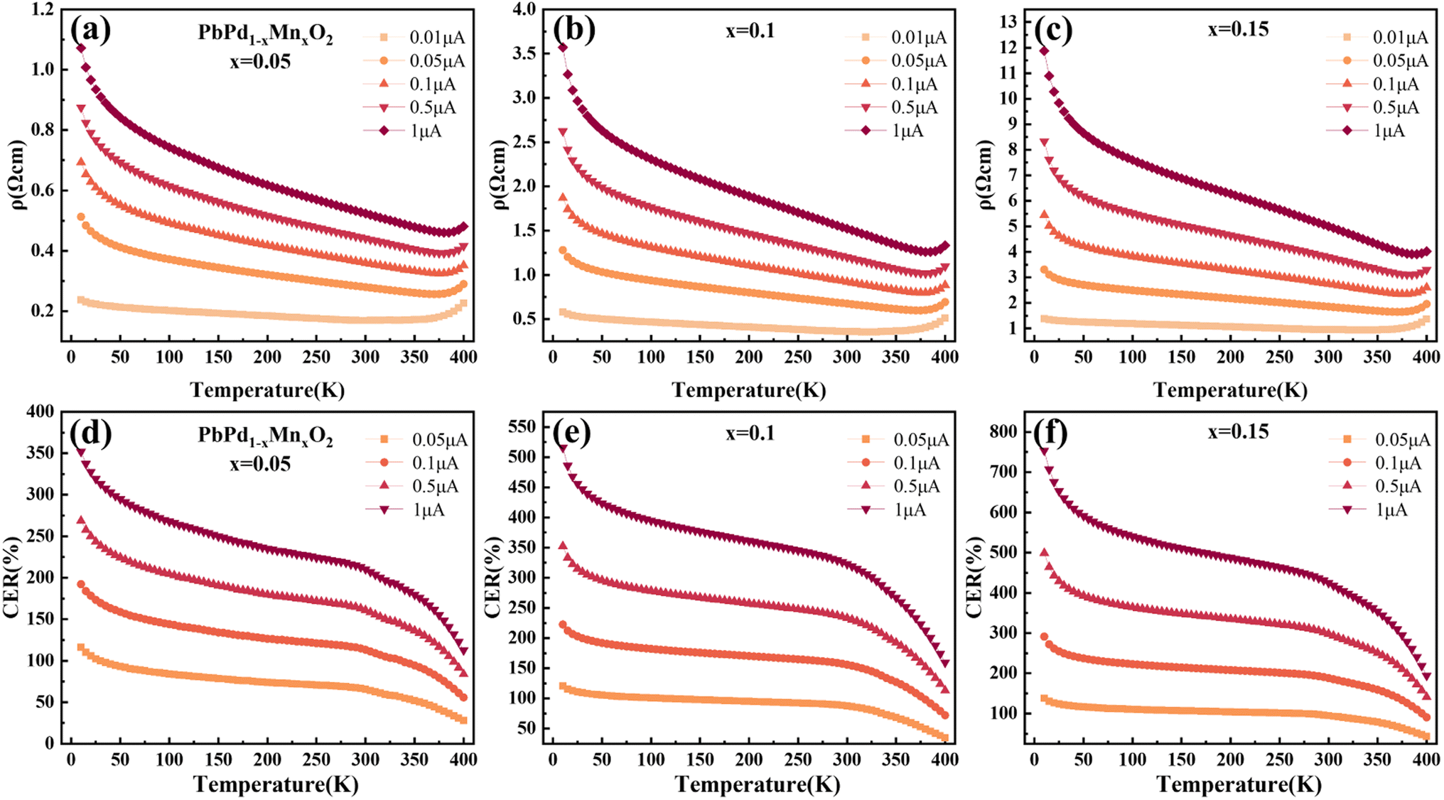 | ||
| Fig. 2 Temperature dependence of the resistivity of PbPd1−xMnxO2 (x = 0.05, 0.1, 0.15) thin films at different applied currents, (a) x = 0.05, (b) x = 0.1, (c) x = 0.15. Temperature dependence of CER value of PbPd1−xMnxO2 (x = 0.05, 0.1, 0.15) films, (d) x = 0.05, (e) x = 0.1, (f) x = 0.15. | ||
In Fig. 2(d)–(f), the temperature-dependent curve of CER is plotted according to the definition of the equation:31–33
 | (1) |
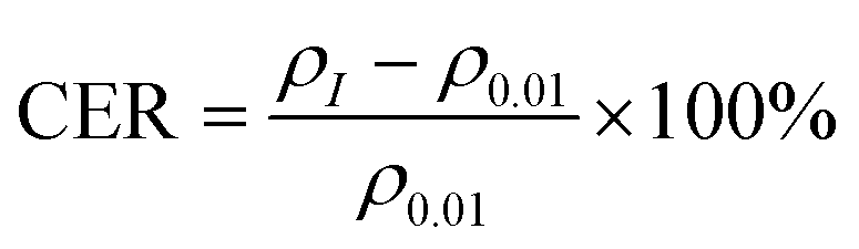
In order to explain the mechanism of the CER for PbPdO2 thin film, we established the internal electrical field model.22 In this model, it is suggested that an internal electric field forms around the O1− holes due to the existence of Pb vacancy, and the O1− holes are beneficial to the transport of charge carriers. However, there exists a critical temperature Tc. When the temperature is lower than Tc, the energy of electrons is not enough to cross the barrier of the built electric field, so it will not affect the electrical transport. When the temperature is higher than Tc, driven by temperature and current, electrons will overcome the barrier of the built electric field and enter the O1− hole to turn it into O2−, thus eliminating the built electric field. As a result, the band gap increases and positive CER is generated. Fig. 3(a)–(c) show the temperature-dependent resistivity of PbPd1−xMnxO2 (x = 0.05, 0.1, 0.15) thin films for four heating and cooling cycles in the temperature range of 10–400 K at a current of 0.01 μA. The first cycle is heating from 10 K to 400 K (named 1sth) and cooling from 400 K to 10 K (named 2ndc). Then, the second heating and cooling cycle is named 3rdh and 4thc, respectively, and so on. The enlarged graphs between 300 K and 400 K in Fig. 3(a)–(c) are shown in Fig. 3(d)–(f), respectively. From the figures, it can be found that the resistivity value of the cooling curve of each cycle is greater than that of the heating curve. The cooling curve of the first cycle (2ndc) and the heating curve of the second cycle (3rdh) overlap at the temperature range <340 K, and there exists also a transition temperature, Tc. When T > Tc, the sample resistivity increases drastically, resulting in curve separation, while the overlap of curves at the temperature range of T < Tc indicates that cycling at this temperature does not affect the resistivity of the material. The similar behaviors were also observed in 4thc and 5thh, as well as 6thc and 7thh. In Fig. 3(d)–(f), it can be found that the transition temperature of the three films is about 340 K, which is higher than the Tc with 260 K observed in pure PbPdO2 films,22 which means that higher energy is required for the electron injection into the Mn-doped PbPdO2 thin films. However, the transition temperature of Mn-doped films with different concentrations did not change significantly, indicating that Mn-doping concentration did not have a great effect on the transition temperature.
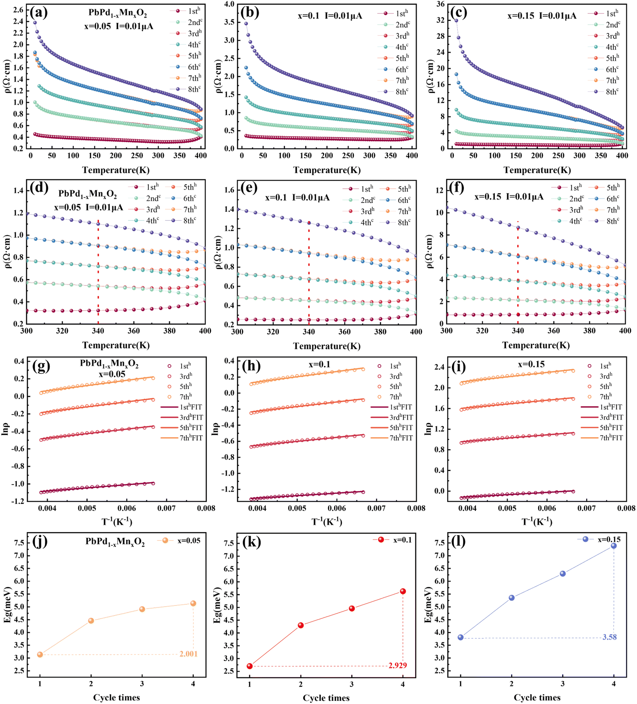 | ||
Fig. 3 ρI (T) cycle curves of PbPd1−xMnxO2 (x = 0.05, 0.1, 0.15) films at 0.01 μA constant current, (a) x = 0.05, (b) x = 0.1, (c) x = 0.15; 240–400 K temperature regions in (a), (b) and (c) are enlarged in (d), (e) and (f), respectively; based on the Arrhenius formula fit ln![[thin space (1/6-em)]](https://www.rsc.org/images/entities/char_2009.gif) ρ as a function of T−1 (150 K < T < 260 K), (g) x = 0.05, (h) x = 0.1, (i) x = 0.15; The changes of Eg values of the three films with the increase of cycle times (1sth, 3rdh, 5thh, 7thh curves representing the first, second, third, and fourth cycles, respectively), (j) x = 0.05, (k) x = 0.1, (l) x = 0.15. ρ as a function of T−1 (150 K < T < 260 K), (g) x = 0.05, (h) x = 0.1, (i) x = 0.15; The changes of Eg values of the three films with the increase of cycle times (1sth, 3rdh, 5thh, 7thh curves representing the first, second, third, and fourth cycles, respectively), (j) x = 0.05, (k) x = 0.1, (l) x = 0.15. | ||
We selected 1sth, 3rdh, 5thh and 7thh curves in Fig. 3(a)–(c) to represent four heating and cooling cycles respectively for fitting the Arrhenius formula. Select part of the data region with strong linear middle (T = 150–260 K). The specific fitting equation is as follows:34–37
 | (2) |
ρ as a function of T−1 for the three thin films in the temperature range of 150–260 K, respectively. Eqn (2) provides a good fit to the data, indicating that the dominant electron transport mechanism in PbPd1−xMnxO2 (x = 0.05, 0.1, 0.15) thin films is governed by either thermal activation behavior arising from localized states or band gap-mediated jump processes. By fitting eqn (2), we obtained the band gap value Eg for the heating curves of the three films on four cycles. The results are shown in Fig. 3(j)–(i), respectively. As can be seen from the figures, the band gap of the three films gradually increases with the increase of the cycle numbers. The increases in band gap values and resistivity follow the same trend, thereby providing further substantiation for the existence of thermal activation transport within temperature ranges exceeding Tc. By comparing the band gap values of the three films, it is found that the band gap increases with different amplitudes in the PbPdO2 thin films with different Mn doping concentrations. Taking the difference between the band gap values of the fourth cycle and the first cycle as a reference, the band gap values increased with the increase of doping concentration are 2.001, 2.929 and 3.580 meV for x = 0.05, 0.1, 0.15, respectively. This indicates that Mn doping facilitates the expansion of the band gap in the film. The enhancing value of CER with increasing Mn doping concentration can be well explained as following: The higher the Mn doping concentration, the faster the band gap increases in the temperature region above Tc. As a result, this changed band gap must lead to the increase of the changed resistivity. Thus, the highly doped films exhibits a greater changed rate of resistivity than low-doped films.
DFT calculations show that Mn doping promotes the PbPdO2 system to open the band gap, and the tiny band gap of 0.006 eV from undoped Mn is enhanced to 0.010 eV (as shown in Fig. 4(a) and (b)), which agrees with our experimental results that Mn doping enhances the resistivity of the material in Fig. 2(a)–(c). When the Mn-doped system is changed to −1-valence, which is equivalent to the injection of a charge, the band gap of the system is further increased to 0.096 eV. At the same time, the total energy of the −1-valence system is about 0.271 eV lower than that of the 0-valence system, suggesting that the Mn doping will be favourable for the system to undergo electron injection. As shown in the differential charge density of Fig. 4(d)–(e), the energy reduction of PbPd0.875Mn0.125O2 after the valence change mainly originates from the electron transfer induced by Mn doping. In addition to the significant electron transfer near the Mn atoms before and after the denaturation, there are also simultaneous signs of electron transfer near the Pd atom in the upper left corner of Fig. 4(e). Mn doping facilitates electron injection in the PbPdO2 system, thereby enhancing the positive CER of the materials. The calculated results are in agreement with the experimental results.
 | ||
| Fig. 4 Density of states (DOS) for (a) PbPdO2 (0 valence), (b) PbPd0.875Mn0.125O2 (0 valence) and (c) PbPd0.875Mn0.125O2 (−1 valence) with Pb vacancy. Differential charge densities of the PbPd0.875Mn0.125O2 material −1-valence and 0-valence systems in (d) three-dimensional and (e) two-dimensional forms. | ||
To further investigate the impact of temperature and Mn doping on resistivity, we have conducted measurements of the time-dependent ρt/ρ0 ratio at I = 0.01 μA under different temperatures for a duration of 20 hours. Fig. 5(a)–(c) depicts the time-dependent behavior of the ρt/ρ0 at temperatures of 100 K, 350 K, and 400 K, respectively. Here, ρt and ρ0 denote the resistivity measured at times t and 0, respectively. The ratio of ρt/ρ0 can directly reflect the change of resistivity with time under constant current. At T = 100 K, the ρt/ρ0 for the three films remains almost constant during 20 hours. However, at T = 350 K, the ratio of ρt/ρ0 increases significantly with the increase of measurement time, and the ratio increase more in the higher Mn-doping concentration film, which further confirms the promotion effect of Mn doping on electron injection. It is also proved that the transition temperature Tc exists between 100 K and 350 K. The increase in the ρt/ρ0 ratio at 400 K is more than one order of magnitude greater than that at 350 K, indicating a significant temperature-dependent effect on resistivity under electron injection. It should be noted that the ρt/ρ0 ratio of PbPd0.85Mn0.15O2 thin film at 400 K is lower than that of PbPd1−xMnxO2 (x = 0.05, 0.1) thin films at a longer measurement time. This is due to the high Mn doping concentration, the ρ0 value of the film greatly affects the ρt/ρ0 ratio. However, at a shorter measurement time, the ρt/ρ0 ratio within 2 hours (as shown in the small figure in Fig. 5(c)) can still be observed to show the same pattern as that at 350 K. This is consistent with our previous conclusions. Of course, the thermal resistance effect of up to 100 times remains to be further studied.
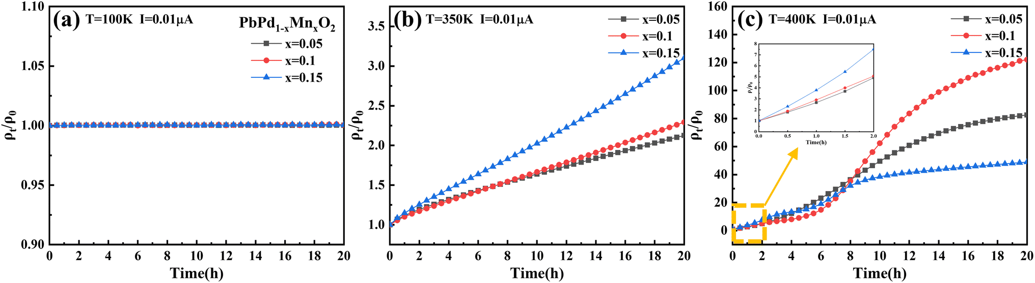 | ||
| Fig. 5 Time dependence of ρt/ρ0 ratio at (a) T = 100 K, (b) T = 350 K and (c) T = 400 K under the applied constant current of 0.01 μA. | ||
The valence change of O element under constant current and temperature change is a good method to verify whether Mn-doped PbPdO2 thin films conform to the changed model from O−1 to O−2. Therefore, we measured in situ XPS spectra of PbPd1−xMnxO2 (x = 0.05, 0.1, 0.15) thin films under constant current. In situ XPS measurements of PbPd1−xMnxO2 (x = 0.05, 0.1, 0.15) thin films were performed under I = 0, 100, 200, 300 μA at T = 300 and 350 K, respectively. Fig. 6 depict the representative in situ XPS spectra of O 1s for PbPd0.95Mn0.05O2 thin film, while the in situ XPS spectra of O 1s for PbPd1−xMnxO2 (x = 0.1, 0.15) thin films are shown in Fig. S2 and S3.† From Fig. 6, one notices that, the O 1s spectrum consists of three peaks located at the binding energies of about 529.50, 531.50 and 534.00 eV. The binding energy of samples was calibrated by carbon at a C 1s peak of 284.8 eV. The spectral peak of about 534.00 eV corresponds to the Pd 3p3/2, which is consistent with the findings of numerous studies on palladium oxides and other relevant studies.38–40 The main peak O(I) of about 529.50 eV is the peak of lattice oxygen, and the secondary peak O(II) of about 531.50 eV is the peak related to oxygen vacancy. According to the area of the peak, the percentage of the O(II) peak (oxygen vacancy) in the total oxygen spectrum peak (O(I) + O(II)) can be calculated, and the calculation results are listed in Table 1. It can be seen from Table 1 that the percentage hardly changes with an increase in current when T = 300 K. When T = 350 K, as the increase of current, the percentage gradually decreases from 44.1% to 42.1%, indicating the transition from O1− to O2−. Similar results have been observed in PbPd1−xMnxO2 (x = 0.1, 0.15) thin films.
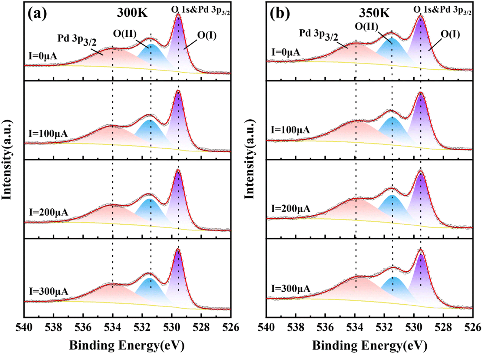 | ||
| Fig. 6 In situ XPS spectra of O 1s of PbPd0.95Mn0.05O2 thin film at 300 K (a) and 350 K (b) under I = 0, 100, 200, 300 μA. | ||
| Current | 300 K | 350 K |
|---|---|---|
| 0 μA | 44.4% | 44.1% |
| 100 μA | 44.4% | 42.9% |
| 200 μA | 44.6% | 42.3% |
| 300 μA | 44.5% | 42.1% |
Quantum transport performance
The low-temperature magnetic transport properties of PbPd1−xMnxO2 (x = 0, 0.05, 0.1, 0.15) thin films were measured. Fig. 7(a)–(d) show the magnetoconductivity (MC) curves of the four films at T = 2, 4, 6, 8 and 10 K. Since quantum transport occurs mainly in low magnetic fields,23,41 we focus on the MC curve in the low magnetic field range. Under low magnetic field conditions, negative cusp MC appears in the temperature range from 2 K to 10 K in PbPdO2 thin film, which is a typical feature of WAL effect. Under the condition of a low magnetic field, PbPd0.95Mn0.05O2 thin film also presents a negative cusp MC between 2 K and 4 K. However, T > 4 K, the MC presents a shape positive cusp, which is characteristic of WL effect. This indicates that there is a temperature-related cross between WAL and WL in PbPd0.95Mn0.05O2 film. The same phenomenon also occurs in Mn-doped films with x = 0.10 and 0.15. The data can be analyzed utilizing the Hikami−Larkin−Nagaoka (HLN) formula presented as following:23–25,42–44
 | (3) |
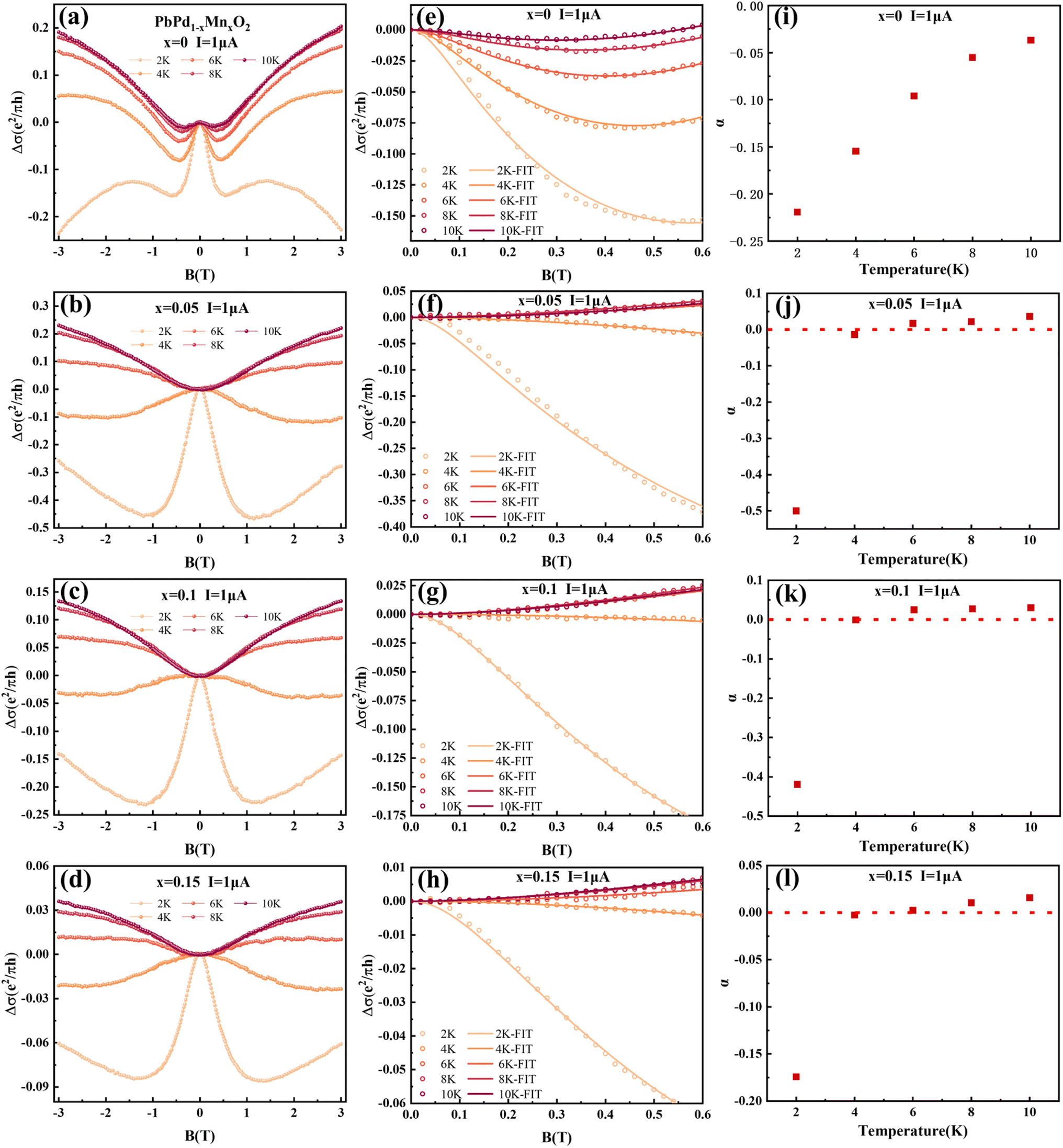 | ||
| Fig. 7 Normalized magnetoconductance (MC) Δσ (B) = σ (B) − σ (0) for PbPd1−xMnxO2 (x = 0, 0.05, 0.1, 0.15) thin films measured at different temperature, for (a) x = 0, (b) x = 0.05, (c) x = 0.1, (d) x = 0.15. Evolution of low field MC as a function of temperature and fitting the HLN equation for the four films for (e) x = 0, (f) x = 0.05, (g) x = 0.1, (h) x = 0.15. The α value distribution obtained by fitting the MC curve with HLN equation at T = 2, 4, 6, 8 and 10 K for (i) x = 0, (j) x = 0.05, (k) x = 0.1, (l) x = 0.15. | ||
Conclusion
PbPd1–xMnxO2 (x = 0.05, 0.1, 0.15) thin films with (002) preferred orientation were prepared. It is found that that Mn doping can increase the value of CER in PbPdO2 thin films by severalfold magnitude, which is also confirmed by first-principles calculations. Moreover, Mn doping enhances the electron injection barrier of PbPdO2 thin film, which induces increasing transition temperature Tc. The speed of band gap opening is enhanced by Mn doping at temperatures higher than Tc, and the rate of enhancement increases with increasing Mn doping concentration. Facilitation of electron injection by Mn doping confirmed by first-principles calculations. The increase of band gap value leads to the increase of resistance, which increases the CER of PbPdO2 thin film. Additionally, based on magnetoresistance measurements, it is observed that Mn-doped film samples exhibit weak localization (WL) and weak anti-localization (WAL) quantum transport characteristics. Mn doping leads to a transition from WAL to WL. Moreover, it is found that, at T = 2 K, the value of α for x = 0.05, 0.1, 0.15 are −0.5, −0.42 and −0.175, which means that a few Mn doping enhances significantly weak anti-localization effect (WAL). However, with increasing Mn concentration, WAL effect is conversely weakened. The implied mechanism on WAL effect and crossover between WAL and WL induced by Mn doping will be further studied.Conflicts of interest
The authors declare that they have no known competing financial interests or personal relationships that could have appeared to influence the work reported in this paper.Acknowledgements
The authors acknowledge the financial support by the National Natural Science Foundation of China (No. 61574037, 11874113, 11344008, 11204038), Industry-university Cooperation Project of Fujian Province (No. 2020H06027) and the Natural Science Foundation of Fujian Province of China (No. 2020J02018).References
- X. L. Wang, Phys. Rev. Lett., 2008, 100, 156404 CrossRef.
- X. Wang, G. Peleckis, C. Zhang, H. Kimura and S. Dou, Adv. Mater., 2009, 21, 2196–2199 CrossRef.
- S. M. Choo, K. J. Lee, S. M. Park, G. S. Park and M. H. Jung, J. Appl. Phys., 2013, 113, 014904 CrossRef.
- D. H. Kim, J. Hwang, E. Lee, K. J. Lee, S. M. Choo, M. H. Jung, J. Baik, H. J. Shin, B. Kim, K. Kim, B. I. Min and J.-S. Kang, Appl. Phys. Lett., 2014, 104, 022411 CrossRef.
- K. Lamontagne Leo, G. Laurita, M. W. Gaultois, M. Knight, L. Ghadbeigi, T. D. Sparks, M. E. Gruner, R. Pentcheva, C. M. Brown and R. Seshadri, Chem. Mater., 2016, 28, 3367–3373 CrossRef.
- X. Chen, Y. Chen, Y. Yang, H. Jia, J.-M. Zhang, S. Chen and Z. Huang, Ceram. Int., 2017, 43, 10428–10433 CrossRef.
- E. B. Qiu, C. Mei, D. C. Ye, Z. Zhang, H. L. Su, Y. C. Wu and J. C. A. Huang, J. Sol-Gel Sci. Technol., 2017, 84, 361–367 CrossRef.
- H. Jia, Y. Yang, W. Zheng, J. M. Zhang, S. Chen and Z. Huang, RSC Adv., 2018, 8, 38751–38757 RSC.
- J.-M. Zhang, X. Chen, H. Jia, Y. Yang, S. Chen and Z. Huang, J. Magn. Magn. Mater., 2019, 485, 271–279 CrossRef.
- F. Tang, C. Mei, P. Chuang, T. Song, H. Su, Y. Wu, Y. Qiao, J.-C.-A. Huang and Y.-F. Liao, Thin Solid Films, 2017, 623, 14–18 CrossRef.
- H. Jia, W. Guo, C. Lin, S. Chen, J. M. Zhang and Z. Huang, J. Magn. Magn. Mater., 2022, 553, 169240 CrossRef.
- K. J. Lee, S. M. Choo, J. B. Yoon, K. M. Song, Y. Saiga, C.-Y. You, N. Hur, S. I. Lee, T. Takabatake and M. H. Jung, J. Appl. Phys., 2010, 107, 09C306 CrossRef.
- F. L. Tang, J. Liu, C. Mei, S. Y. Huang, T. T. Song, H. L. Su, M. K. Lee, Y. C. Wu and J. C. A. Huang, RSC Adv., 2016, 6, 37522–37529 RSC.
- J. A. Kurzman, M.-S. Miao and R. Seshadri, J. Phys. Condens. Matter, 2011, 23, 465501 CrossRef.
- Y. Yang, K. Zhong, G. Xu, J.-M. Zhang and Z. Huang, J. Phys. Condens. Matter, 2019, 31, 405501 CrossRef PubMed.
- T. C. Ozawa, T. Taniguchi, Y. Nagata, Y. Noro, T. Naka and A. Matsushita, J. Alloys Compd., 2005, 395, 32–35 CrossRef.
- K. Lee, S.-M. Choo and M.-H. Jung, Appl. Phys. Lett., 2015, 106, 072406 CrossRef.
- E. Céspedes, G. R. Castro, F. Jiménez-Villacorta, A. de Andrés and C. Prieto, J. Phys. Condens. Matter, 2008, 20, 095207 CrossRef.
- J. H. Li, D. Z. Shen, J. Y. Zhang, D. X. Zhao, B. S. Li, Y. M. Lu, Y. C. Liu and X. W. Fan, J. Magn. Magn. Mater., 2006, 302, 118–121 CrossRef.
- D. Milivojević, J. Blanuša, V. Spasojević, V. Kusigerski and B. Babić-Stojić, Solid State Commun., 2007, 141, 641–644 CrossRef.
- K. Joon Lee, S. M. Choo, Y. Saiga, T. Takabatake and M. H. Jung, J. Appl. Phys., 2011, 109, 5–8 CrossRef.
- H. Jia, Y. Chen, C. Lin, Y. Ruan, S. Chen, J.-M. Zhang and Z. Huang, Ceram. Int., 2021, 47, 26768–26778 CrossRef.
- H.-Z. Lu and S.-Q. Shen, Phys. Rev. B: Condens. Matter Mater. Phys., 2011, 84, 125138 CrossRef.
- E. I. Rogacheva, O. Pavlosiuk, A. V. Meriuts, T. N. Shelest, A. Y. Sipatov, O. N. Nashchekina, K. V. Novak and D. Kaczorowski, Thin Solid Films, 2022, 743, 139070 CrossRef.
- X. Zhang, J. M. Woods, J. J. Cha and X. Shi, Phys. Rev. B, 2020, 102, 1–7 Search PubMed.
- S. M. Choo, K. J. Lee, S. M. Park, J. B. Yoon, G. S. Park, C. Y. You and M. H. Jung, Appl. Phys. Lett., 2015, 106, 1–6 CrossRef.
- G. Kresse and J. Hafner, Phys. Rev. B: Condens. Matter Mater. Phys., 1994, 49, 14251–14269 CrossRef.
- G. Kresse and D. Joubert, Phys. Rev. B: Condens. Matter Mater. Phys., 1999, 59, 1758–1775 CrossRef.
- J. P. Perdew, K. Burke and M. Ernzerhof, Phys. Rev. Lett., 1996, 77, 3865–3868 CrossRef.
- H. J. Monkhorst and J. D. Pack, Phys. Rev. B: Solid State, 1976, 13, 5188–5192 CrossRef.
- A. Odagawa, H. Sato, I. H. Inoue, H. Akoh, M. Kawasaki, Y. Tokura, T. Kanno and H. Adachi, Phys. Rev. B: Condens. Matter Mater. Phys., 2004, 70, 1–4 CrossRef.
- D. S. Shang, J. R. Sun, L. Shi, J. Wang, Z. H. Wang and B. G. Shen, Appl. Phys. Lett., 2009, 94, 21–24 CrossRef.
- W. Wei, Y. Zhu, Y. Bai, H. Liu, K. Du, K. Zhang, Y. Kou, J. Shao, W. Wang, D. Hou, S. Dong, L. Yin and J. Shen, Phys. Rev. B, 2016, 93, 3–6 Search PubMed.
- X. Zhang, S. Sun and H. Lei, Phys. Rev. B, 2017, 95, 035209 CrossRef.
- J. Xing, H. Cao, A. Paul, C. Hu, H. H. Wang, Y. Luo, R. Chaklashiya, J. M. Allred, S. Brown, T. Birol and N. Ni, Phys. Rev. Mater., 2020, 4, 1–8 Search PubMed.
- S. Li, H. Zhao, D. Li, S. Jin and L. Gu, J. Appl. Phys., 2015, 117, 205101 CrossRef.
- Y. Zhang, C. Michioka, M. Imai, H. Ueda and K. Yoshimura, J. Phys.: Conf. Ser., 2017, 868, 012025 CrossRef.
- H. K. K. Nguyen, R. Addou, K. C. Chukwu, G. S. Herman and L. Árnadóttir, J. Phys. Chem. C, 2023, 127, 11472–11480 CrossRef.
- X. Li, X. Wang, K. Roy, J. A. Van Bokhoven and L. Artiglia, ACS Catal., 2020, 10, 5783–5792 CrossRef.
- R. Toyoshima, M. Yoshida, Y. Monya, Y. Kousa, K. Suzuki, H. Abe, B. S. Mun, K. Mase, K. Amemiya and H. Kondoh, J. Phys. Chem. C, 2012, 116, 18691–18697 CrossRef.
- H.-Z. Lu and S.-Q. Shen, Chinese Phys. B, 2016, 25, 117202 CrossRef.
- S. Hikami, A. I. Larkin and Y. Nagaoka, Prog. Theor. Phys., 1980, 63, 707–710 CrossRef.
- J. Chen, H. J. Qin, F. Yang, J. Liu, T. Guan, F. M. Qu, G. H. Zhang, J. R. Shi, X. C. Xie, C. L. Yang, K. H. Wu, Y. Q. Li and L. Lu, Phys. Rev. Lett., 2010, 105, 1–4 Search PubMed.
- D. Weißhaupt, H. S. Funk, M. Kern, M. M. Dettling, D. Schwarz, M. Oehme, C. Sürgers, J. van Slageren, I. A. Fischer and J. Schulze, J. Phys.: Condens.Matter, 2021, 33, 085703 CrossRef.
Footnote |
| † Electronic supplementary information (ESI) available. See DOI: https://doi.org/10.1039/d3ra08039k |
| This journal is © The Royal Society of Chemistry 2024 |