
 Open Access Article
 This Open Access Article is licensed under a
 Creative Commons Attribution 3.0 Unported Licence
Highly responsive and selective ozone sensor based on Ga doped ZnS–ZnO composite sprayed films
T. Laribia,
R. Souissi *b,
S. Bernardinic,
M. Bendahanc,
N. Bouguilaa and
S. Alayaa
*b,
S. Bernardinic,
M. Bendahanc,
N. Bouguilaa and
S. Alayaa
aUniversité de Gabès, Laboratoire de Physique des Matériaux et des Nanomatériaux appliqué à l'environnement, Faculté des Sciences de Gabès, Cité Erriadh, Zrig, 6072, Gabès, Tunisia
bCarthage University, Laboratoire des Matériaux, Molécules et Applications IPEST, BP51, La Marsa 2070, Tunis, Tunisia. E-mail: riadhsouissi1@gmail.com
cAix Marseille Univ, CNRS, IM2NP, Marseille, France
First published on 2nd January 2024
Abstract
Ozone detection is currently the subject of wide scientific and technological research, motivated by its harmful impact on human safety, environment and health. With the aim of searching for new highly sensitive materials for ozone detection, Ga-doped ZnS and ZnS–ZnO films were deposited by a spray pyrolysis technique. The obtained films were annealed at 400 °C for two hours. The ozone sensing properties were investigated by measuring the sensor resistance for several ozone concentrations ranging from 30 to 120 ppb. The sensor response reveals a dependence on the gallium concentration. The best response was obtained with 4% doping gallium. The sensitivity is 4.5 ppb−1 at 260 °C and the response to 30 ppb ozone is 150. Moreover, the sensor shows high performance such as good selectivity and fast rapidity.
1 Introduction
In recent years, zinc sulfide (ZnS) and zinc oxide (ZnO) have garnered significant interest as highly promising II–VI semiconductor compounds with excellent characteristics. They exhibit a range of properties that contribute to their potential for fabricating photonic, optical, and electronic devices such as solar cells,1,2 window layers3,4 and photocatalysis.5 With a wide bandgap ranging from 3.54 to 3.91 eV and from 3.37 to 3.72 eV for ZnS and ZnO respectively, heterostructures of these compounds are candidates for ultraviolet lasers and detectors.6,7 In the literature, ZnS/ZnO compounds have been reported to be fabricated by different methods, such as: ZnS/ZnO heterostructures synthesized via a simple thermal evaporation method,6,8 ZnS–ZnO nanocomposites through the hydrothermal route,9 coaxial nanowires and hierarchical nanowires by chemical bath deposition and chemical etching processes, respectively,10 and ZnS/ZnO films via pulsed laser deposition.11 In another study,12 ZnS/ZnO:Mn layers were prepared by thermal sulfidation of ZnO:Mn films deposited on a Si substrate with an RF magnetron sputtering technique. In addition, Deepa et al.13 have deposited zinc sulfide thin films by ultrasonic spray pyrolysis. Obtained films have traces of the ZnO phase together with the dominant ZnS phase. Among these methods, spray pyrolysis is an interesting deposition technique for preparing ZnS/ZnO thin films. Indeed, it is a simple and an inexpensive technique to obtain optically smooth, uniform and homogeneous layers.Recently, researchers have shown that ZnS/ZnO could be a good candidate for gas detection. Tsai et al.14 reported that ZnO/ZnS core–shell structures hydrothermally grown on SiO2 substrates show promise for future hydrogen sensing applications. More recently,15 they demonstrated that CO gas sensing measurements revealed that incorporation of a ZnS shell on ZnO nanorods can increase gas sensing capability. In another work, Ding et al.16 reported that ZnO nanowires were modified with an optimal amount of ZnS to form nanostructured heterojunctions for high-performance H2S gas sensing. Furthermore, Park et al.17 reported that ZnS-core/ZnO-shell nanowires demonstrate substantial improvement in the response to NO2 gas by UV irradiation. As ozone (O3) is a derivative gas from NO2, to the best of our knowledge, there is no report on the characterization of ZnS/ZnO in ozone sensing application. This prompts us to investigate ZnS/ZnO within the framework of this goal in this report. Ozone plays a vital role in supporting life as it acts as a primary UV protective layer in the stratosphere. It is a significant environmental pollutant, known to cause detrimental effects on human health even at low concentrations. Exposure to tropospheric ozone can lead to irritation of the eyes, nose and throat, as well as respiratory issues such as coughing and headaches.18,19 To ensure the well-being of the public, the World Health Organization (WHO) has established guidelines limiting exposure to ozone at a maximum average concentration of 100 μg m−3 (50 parts per billion, ppb) for 8 hours period.20 Additionally, for the protection of vegetation, the European directive employs an accumulated ozone over the threshold of 80 μg m−3 (40 ppb, designed as AOT40). Several materials have already been studied for ozone detection such as Co3O4,21 ZnO/SnO2,22 In2O3,23 WO3 (ref. 24) and CuAlO2.25 Generally, the selectivity of the sensors can be adjusted over a wide range by varying several aspects such as the crystal structure and morphology, the dopants used,26 the contact geometries,27 the operating temperature or the operation mode.24
In this paper, we demonstrate that ZnS–ZnO material is a good ozone sensor. Gallium doping improves its performances at high temperature (260 °C) and leads also to ozone detection at lower temperatures down to 120 °C. The sensing properties of the prepared films were studied using DC electrical characterization.
2 Experimental
ZnS–ZnO films were grown on Si/SiO2 substrates using the spray pyrolysis technique. This method is a simple and cost effective-way to deposit large area thin films at moderate temperatures (100–500 °C). The films were prepared by spraying an aqueous solution onto the substrates. The solution contained zinc chloride (ZnCl2) and thiourea [SC(NH2)2], as sources of Zn2+ and S2− ions, respectively, with an initial Zn:S molar ratio of 1. Distilled water was used as a solvent. To achieve various levels of gallium (Ga) doping, gallium sulphate Ga2(SO4)3 with three different concentrations (0%, 2% and 4% atomic concentration) was added to the starting solution. The substrates were placed on a hotplate and heated gradually from ambient temperature until reaching the desired deposition temperature of 350 °C. This gradual heating helps prevent thermal shock. The spray duration was kept at 3 minutes. The distance between the spray nozzle and the substrate was fixed at 25 cm to ensure proper coverage of the substrate surfaces. During the deposition, the solution and nitrogen carrier gas flow rates were maintained at 2 ml min−1 and 10 l min−1, respectively. The formation of ZnS is given by the following equation:| ZnCl2 + SC(NH2)2 + 2H2O → ZnS + 2NH4Cl + CO2 | (1) |
After deposition, thin films were annealed at 400 °C in an electric furnace under atmospheric air. The purpose of this annealing was to improve crystallization and stability of the sensitive films. The heating rate was fixed at 10 °C min−1 to reach 400 °C, which was maintained for 2 h. Then, the cooling was carried out in atmospheric air within the furnace. To measure the electrical resistance of the sensors, transducer platforms were used. These platforms had two interdigitated Pt/Ti electrodes sputtered on a Si/SiO2 substrate, as shown in Fig. 1a. The interdigitated electrodes consisted of thirty rectangular platinum fingers on a 4 × 4 mm2 substrate area, with 50 μm gap and finger width.
 | ||
| Fig. 1 (a) Photo of platform for transducers and (b) ozone detection experimental set-up. | ||
The microstructure of the deposited films was analyzed by X-ray diffraction, using a Bruker D8 Advance diffractometer, with a monochromatic Cu-Kα radiation (λ = 1.5406 Å). The angle 2θ was varied from 20° to 70° during the measurements. The morphological characterization was performed by scanning electron microscopy (SEM), using a Zeiss FE-SEM ULTRA plus microscope with an attached electron dispersive spectrometer (EDS) for chemical composition analysis.
The ozone sensing properties of the samples were investigated using the experimental set-up shown in Fig. 1b. To produce ozone gas, a UV pen ray lamp (UVP/185 nm stable ozone generator) was used. Dry air was led through a quartz tube. When illuminated by a UV lamp, some of the oxygen molecules were transformed into ozone. The UV illumination was modified by moving the shutter around the lamp. Several ozone concentrations in the range of 30 ppb to 120 ppb were obtained while maintaining the dry air flow at a fixed rate of 0.5 l min−1. Calibration of ozone concentrations was ensured by an Seres 2000G ozone analyzer. The sensors were exposed to ozone for 3 minutes. The operating temperature was regulated by a heat source from 120 to 260 °C. Indeed, the sensor is brought to working temperature using a resistance covered with ceramic acting as a sample holder and controlled by a stabilized generator. The heating is adjusted manually and the heating rate is practically 10° min−1. A Pt100 probe, fixed in the vicinity of the sample and connected to an ohmmeter, is used to display the sensor temperature. The sensors were polarized at 1 V. The resistance measurements were performed using a Keithley 2450 source-meter.
In order to calculate the response of the ZnS sensors, based on the change in resistance, we applied eqn (2) and (3) for oxidant and reducing gases, respectively:
 | (2) |
 | (3) |
Sensitivity is defined by the following formula:
 | (4) |
3 Results and discussion
3.1. Physical characterization
 | ||
| Fig. 2 X-ray diffraction patterns thin films for different Ga concentrations. | ||
Structural parameters such as crystallite size D, dislocation density δ and microstrain ε were estimated from the XRD profiles for the preferred orientation (002).
Assuming spherical crystallites, their size can be estimated using Debye–Scherrer's formula as follows:26
 | (5) |
The dislocation density was calculated using the formula:
 | (6) |
The microstrain was deduced from the following relation:
 | (7) |
The calculated values of D, δ and ε are summarized in Table 1. The crystallite size is approximately 18 nm. The increase in micro-stress is attributed to the doping.
| Sample | D (nm) | δ (1010 lines per cm2) | ε |
|---|---|---|---|
| ZnS–ZnO:Ga2% | 17 | 35 | 0.007 |
| ZnS–ZnO:Ga4% | 19 | 26 | 0.062 |
 | ||
| Fig. 3 EDS spectra of (a) undoped, (b) Ga2% doped ZnS–ZnO, (c) Ga4% doped ZnS–ZnO thin films. | ||
 | ||
| Fig. 4 SEM graphs of (a) undoped, (b) ZnS–ZnO:Ga2% and (c) ZnS–ZnO:Ga4% thin films. | ||
 | ||
| Fig. 5 (a) Optical transmittance spectra, inset absorbance spectra, (b) Tauc plots of samples. | ||
The absorption spectra were used to calculate the optical band gap energies of the films using Tauc expression:32
 | (8) |
We have studied the evolution of (αhν)2 as a function of the photon energy hν for the different layers (Fig. 5b). The extrapolation of the linear zone of the obtained curve to the horizontal axis (αhν = 0) gives us a good estimate of the bandgap energy. The evaluated Eg of undoped sample is equal to 3.84 eV, which decreases slightly with doping to 3.74 eV. The bandgap energy of the undoped sample is larger than that reported for bulk ZnS. This is due to residual stress.33 This result is consistent with previous studies by Poornaprakash et al. (3.93–3.70 eV)34 and Wei et al. (3.87–3.76 eV).35
3.2. Ozone sensing study
 | ||
| Fig. 6 Dynamic change of electrical resistance during repetitive cycles of alternating exposure to 120 ppb ozone and dry air at 260 °C: (a) undoped, (b) ZnS–ZnO:Ga2% and (c) ZnS–ZnO:Ga4% thin films. | ||
We can observe that the resistance of all films increases during exposure to O3 and decreases when dry air is reintroduced into the test chamber. This behavior is the result of adsorption–desorption phenomenon of an oxidizing gas on the surface of an n-type semiconductor.36 We also note that the baseline is stable, and all samples have good repeatability indicating the material's potential to detect O3 gas. We suggest that the detection mechanism can be explained by dissociative adsorption alone for triatomic gas. Firstly, when ozone is added to the atmospheric gas, O3 molecules adsorb on the surface sites of the sensitive layer according to the following equation:
| O3 + e− → O2 + O− | (9) |
The trapping of electrons by ozone leads to a decrease of free electron concentration and as a consequence, resistance increases.
In the other side, during the introduction of dry air, O− is desorbed from the surface of the material into the gas phase in the form of ozone molecules as shown in the following equation:
| O− + O2 → O3 + e− | (10) |
3.2.2.1 Response. In order to monitor the effect of the working temperature on the ozone sensor response, the films were heated to five temperatures ranging from 120 °C to 260 °C.
Fig. 7a illustrates the resistance change of undoped ZnS sample over time for 120 ppb ozone at 260 °C. Below this temperature, the material exhibits high resistance and no signal can be recorded. It now states that the resistance is very high below a certain temperature and it cannot be measured by the Keithley nanoammeter. Fig. 7b and c illustrate the dynamic change in sensor resistance for 120 ppb of ozone at five operating temperatures. We can note that the resistance base line diminishes by rising operating temperature, confirming the semiconductor behavior of the material. Fig. 7d shows that the response increases from 1.7 to 50 for ZnS–ZnO doped Ga2% and from 5.6 to 540 for ZnS–ZnO doped Ga4% by increasing the operating temperature from 120 to 260 °C. While, the undoped layer shows a weak response of 2.8 at an operating temperature of 260 °C. In fact, we think that as the temperature increases, the electron density of the ZnS–ZnO composite increases resulting of the electrons emission from donor levels matching sulfur vacancies, oxygen vacancies and interstitial Zn to the conduction band. This increase in the concentration of free electrons promotes the chemisorption of O3 molecules according to eqn (9). In addition, gallium (Ga) is located in group 13, so it therefore has 3 valence electrons, while the zinc has two only. Most importantly, the higher the doping level gets, the higher of the electron density in the ZnS–ZnO composite which further improves the ozone adsorption.37 As a result, the sensing response and layer conductivity can be enhanced by Ga doping. ZnS–ZnO:Ga4% is our best candidate to detect ppb level ozone gas.
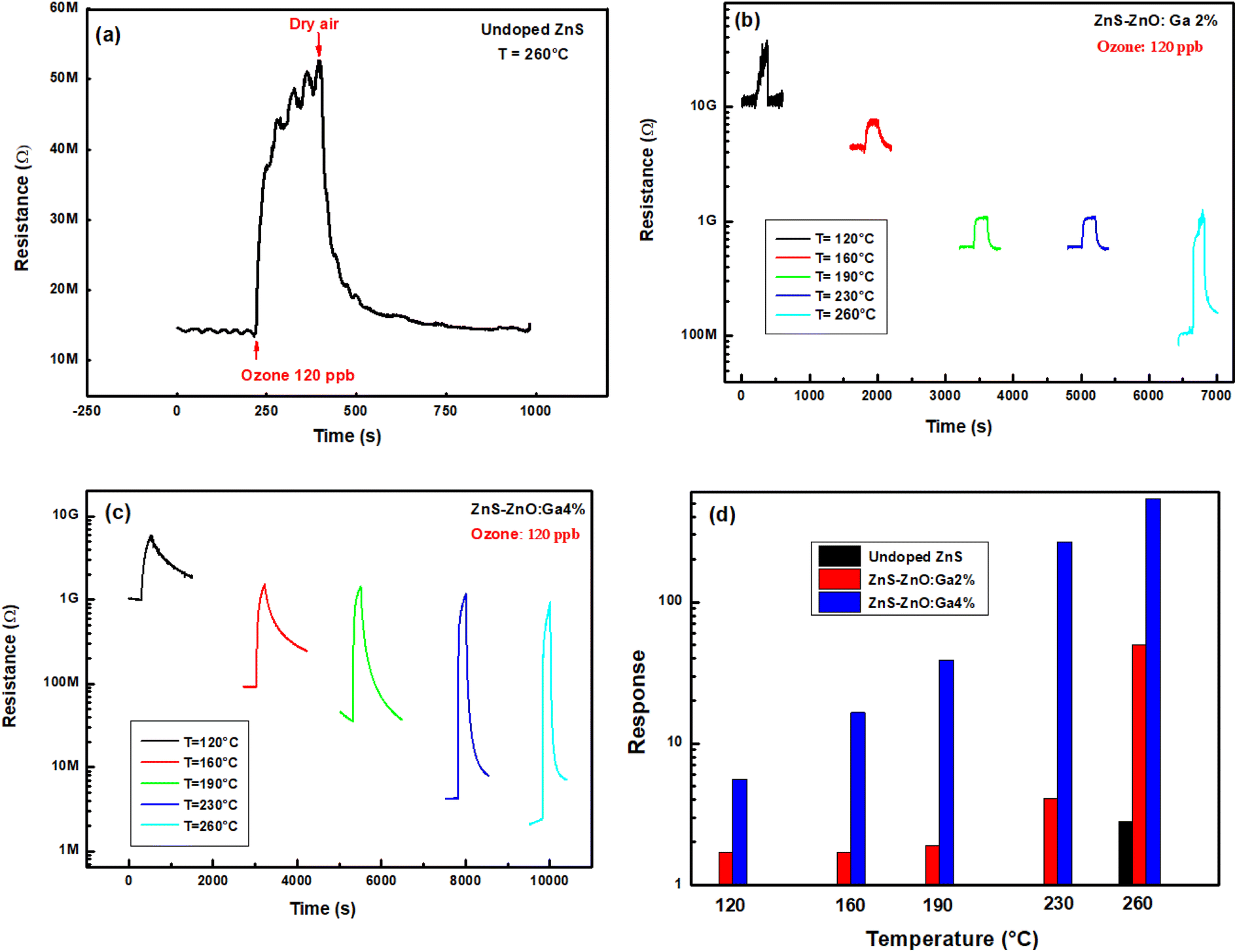 | ||
| Fig. 7 Dynamic change of sample resistance to 120 ppb O3 at five working temperatures, (a) undoped, (b) ZnS–ZnO:Ga2%, (c) ZnS–ZnO:Ga4% thin films and (d) response versus temperature to 120 ppb ozone. | ||
3.2.2.2 Sensitivity. The experiment was conducted with four different ozone concentrations: 30, 65, 100, and 120 ppb. The sensors were operated at working temperature of 260 °C.
Fig. 8(a–c) show the dynamic response of the sensors to the different ozone concentrations. These results indicate that there is a proportionality between the response of the sensors and the concentration of ozone. We observed that the response of the undoped layer increased from 1.5 to 2.8 by increasing the ozone concentration from 30 ppb to 120 ppb. For ZnS–ZnO:Ga2%, the response increased from 28 to 55. The best response was obtained with the ZnS–ZnO:Ga4% sample, which showed an increase in response from 140 to 540 by increasing the ozone concentration in the same range. Fig. 8d depicts the evolution of the sensor response as a function of ozone concentration. The response is linearly proportional to O3 concentration. The sensitivity of the sensor is calculated from the slope of the fitted line and is equal to 0.01 ppb−1, 0.3 ppb−1, and 4.2 ppb−1 corresponding to undoped ZnS, ZnS–ZnO:Ga2%, and ZnS–ZnO:Ga4%, respectively. Consequently, gallium doping improves both sensitivity and response and can be suitable for gas applications.
 | ||
| Fig. 8 Dynamic response of samples at a working temperature of 260 °C for four concentrations of ozone, (a) undoped, (b) ZnS–ZnO:Ga2%, (c) ZnS–ZnO:Ga4% thin films and (d) response versus ozone concentration. | ||
3.2.2.3 Rapidity. The sensor's performance can be evaluated in terms of its response and recovery times, which are important indicators of its rapidity. The response time is defined as the time necessary for the sensor to achieve 90% of the response reaching a saturate state, and the recovery time represents the time to return to 10% of the baseline after exposure to ozone.
Fig. 9a illustrates the evolution of response and recovery times versus working temperature of a ZnS–ZnO:Ga4% sensor exposed to 120 ppb of ozone. It can be noted that the response time is in the order of 160 seconds and the recovery time decreases from 1860 s to 45 s by rising the operating temperature from 120 °C to 260 °C. In fact, when energy is supplied to a system, the temperature rises, which can accelerate the chemical reactions controlling gas adsorption and desorption at the semiconductor surface. With this, the activation energy for the recovery process can be calculated from the dependence of recovery time as a function of temperature, using the well-known Arrhenius equation:
 | (11) |
 | ||
| Fig. 9 (a) Response time and recovery time of ZnS:Ga4% sensor upon exposure to 120 ppb O3 depending on the working temperature. (b) Arrhenius plots of recovery process. | ||
Fig. 9b reveals that ln(τrec) varies linearly with 1000/T, indicating that the estimated value of the activation energy for the recovery process is 0.5 eV, which is higher than the thermal energy at room temperature (Eth = 0.025 eV). This result suggests that ozone desorption process is difficult and recovery time is high at low temperature.
3.2.2.4 Selectivity. The selectivity of a sensor refers to its ability to specifically respond to a particular gas in the presence of other gases. To investigate the selectivity of the ZnS–ZnO:Ga4% sensor, the last was exposed to various volatile organic compounds (VOCs) at 500 ppm concentration and nitrogen dioxide (NO2) at 120 ppb at a working temperature of 260 °C. Fig. 10a displays the current change versus time as the sensor undergoes alternating cycles of exposure to VOCs and dry air. The results of obtained response are illustrated by the histogram in Fig. 10b. We have also reported the response of the same sample for an ozone and a nitrogen dioxide concentration of 120 ppb. The results clearly demonstrate the high selectivity of the ZnS–ZnO:Ga4% sensor towards ozone in presence of VOCs and nitrogen dioxide.
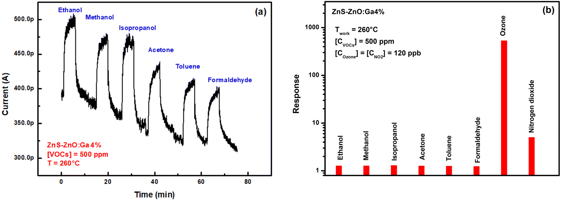 | ||
| Fig. 10 (a) Dynamic change of current to 500 ppm VOCs at 260 °C for ZnS–ZnO:Ga4% sensor, (b) selectivity of ZnS–ZnO:Ga4% sensor. | ||
A comparative analysis of the sensing properties of the developed ZnS–ZnO:Ga4% sensor with previously published ozone sensors is presented in Table 2.38–43 The results highlight that ZnS–ZnO:Ga4% sensor outperforms other ozone sensors in terms of detection sensitivity. Specifically, it shows promising potential for detecting ozone gas.
| Materials | T (°C) | LOD (ppb) | Response | τresp/τrec (s) | Year | Ref. |
|---|---|---|---|---|---|---|
| β-In2S3 | 160 | 40 | 1.5 | 147/414 | 2022 | 7 |
| In2O3 | 70 | 200 | 5 | —/— | 2021 | 38 |
| ZnO | 250 | 60 | 3 | 9/300 | 2015 | 39 |
| CuWO3 | R.T. | 90 | 10 | —/— | 2018 | 40 |
| rGo/ZnO | R.T. | 300 | 1.97 | —/— | 2018 | 41 |
| Carbon nanotubes | 300 | 80 | 1.3 | —/— | 2019 | 42 |
| rGo–ZnO | R.T. | 100 | 49.9 | —/— | 2021 | 43 |
| ZnS–ZnO:Ga4% | 120 | 120 | 5 | 160/1860 | 2023 | This work |
| ZnS–ZnO:Ga4% | 260 | 30 | 150 | 160/45 | 2023 | This work |
4 Conclusion
In this work, undoped and Ga-doped ZnS–ZnO thin films were deposited on SiO2/Si substrates with inter-digitated platinum electrodes by spray pyrolysis technique at a temperature of 350 °C. The effect of Ga doping on structural, morphological, optical and ozone gas sensing properties has been reported. The findings indicate the amorphous structure for the undoped films while with Ga doping the films present two hexagonal phases: ZnS and ZnO. Doping improves considerably crystallinity and the average crystallite size was evaluated to be 18 nm. In terms of surface morphology, the undoped sample was homogenous and smooth, but with doping, it became porous and granular. Moreover, the optical transmission was high in the visible region and reaches 90% in value. The gap energy decreased from 3.84 eV to 3.74 eV by doping. Finally, the ozone detection performances were evaluated. The best properties were found with ZnS–ZnO:Ga4% sensor. At 260 °C working temperature, the response to 30 ppb ozone is 150, the sensitivity is 4.5 ppb−1, the response recovery times were found to be 160 s and 45 s respectively. This study suggests that the gallium-doped ZnS–ZnO composite deposited by spray pyrolysis pathway has the potential for highly sensitive and ppb level ozone detection. Nevertheless, these results are encouraging for deepening the study of sensing mechanism to improve performances of ZnS–ZnO:Ga promising sensor.Ethical statement
The authors have no potential conflict of interest to disclose.Data availability
The datasets generated during and/or analyzed during the current study are available from corresponding author on reasonable request.Author contributions
Conceptualization: N. Bouguila, R. Souissi, M. Bendahan. Acquisition of data: T. Laribi, S. Bernardini, R. Souissi. Formal analysis: T. Laribi, R. Souissi, N. Bouguila, S. Bernardini, M. Bendahan, S. Alaya. Methodology: T. Laribi, R. Souissi, S. Bernardini. Supervision: N. Bouguila, R. Souissi. Validation: T. Laribi, R. Souissi, S. Bernardini, M. Bendahan, N. Bouguila, S. Alaya. Writing original draft: T. Laribi, R. Souissi, N. Bouguila. Writing review & editing: M. Bendahan, S. Bernardini, S. Alaya.Conflicts of interest
There are no conflicts to declare.Acknowledgements
The authors declare that no funding, grant, or other support was received during the preparation of this manuscript.References
- Q. Zhang, C. S. Dandeneau, X. Zhou and G. Cao, ZnO Nanostructures for Dye-Sensitized Solar Cells, Adv. Mater., 2009, 21, 4087–4108, DOI:10.1002/adma.200803827
.
- P. M. Mana, P. K. Bhujbal and H. M. Pathan, Fabrication and Characterization of ZnS based Photoelectrochemical Solar Cell, ES Energy Environ., 2021, 12, 77–85, DOI:10.30919/esee8c1021
- S. Hamrouni, M. S. AlKhalifah and M. S. El-Bana, et al., Deposition and characterization of spin-coated n-type ZnO thin film for potential window layer of solar cell, Appl. Phys. A, 2018, 124, 555, DOI:10.1007/s00339-018-1980-z
- A. A. Faremi, A. T. Akindadelo, M. A. Adekoya, A. J. Adebayo, A. O. Salau, S. Samuel Oluyamo and P. A. Olubambi, Engineering of window layer cadmium sulphide and zinc sulphide thin films for solar cell applications, Results Eng., 2022, 16, 100622, DOI:10.1016/j.rineng.2022.100622
- Li X. Yin, D. Zhang, J. Ma, X. Kong, J. Huang, H. Zhang and C. Liu, Facile synthesis and characterization of ZnS nano/microcrystallites with enhanced photocatalytic activity, Powder Technol., 2016, 301, 1085–1091, DOI:10.1016/j.powtec.2016.07.058
- J. Yan, X. Fang, L. Zhang, Y. Bando, U. K. Gautam, B. Dierre, T. Sekiguchi and D. Golberg, Structure and Cathodoluminescence of Individual ZnS/ZnO Biaxial Nanobelt Heterostructures, Nano Lett., 2008, 8, 2794–2799, DOI:10.1021/nl801353c
- S. R. Chalana, R. Vinodkumar, I. Navas, V. Ganesan and V. P. Mahadevan Pillai, Influence of argon ambience on the structural, morphological and optical properties of pulsed laser ablated zinc sulfide thin films, J. Lumin., 2012, 132, 944–952, DOI:10.1016/j.jlumin.2011.10.017
- L. Hu, J. Yan, M. Liao, H. Xiang, X. Gong, L. Zhang and X. Fang, An Optimized Ultraviolet-A Light Photodetector with Wide-Range Photoresponse Based on ZnS/ZnO Biaxial Nanobelt, Adv. Mater., 2012, 24, 2305–2309, DOI:10.1002/adma.201200512
- S. Ali, S. Saleem, M. Salman and M. Khan, Synthesis, structural and optical properties of ZnS–ZnO nanocomposites, Mater. Chem. Phys., 2020, 248, 122900, DOI:10.1016/j.matchemphys.2020.122900
- Y. Xue-Lian, J.-G. Song, Y.-S. Fu, Y. Xie, X. Song, J. Sun and X.-W. Du, ZnS/ZnO Heteronanostructure as Photoanode to Enhance the Conversion Efficiency of Dye-Sensitized Solar Cells, J. Phys. Chem. C, 2010, 114, 2380–2384, DOI:10.1021/jp910355m
- C. Wang, Fabrication and optical-electrical characteristics of ZnS/ZnO films by pulsed laser deposition, Thin Solid Films, 2023, 780, 139971, DOI:10.1016/j.tsf.2023.139971
- Y.-T. Nien, S.-C. Tsai and I.-G. Chen, ZnS/ZnO:Mn phosphor layer produced by thermal sulfidation of RF magnetron sputtered ZnO:Mn films, J. Cryst. Growth, 2006, 287, 128–133, DOI:10.1016/j.jcrysgro.2005.10.055
- K. G. Deepa, M. Sunil Anantha and N. Jampana, Highly transparent ZnS buffer layer prepared by ultrasonic spray pyrolysis for photovoltaic applications, J. Anal. Appl. Pyrolysis, 2017, 126, 188–193, DOI:10.1016/j.jaap.2017.06.009
- Y.-S. Tsai, T.-W. Chou, C. Y. Xu, W. C. Huang, C. F. Lin, Y. C. S. Wu, Y.-S. Lin and H. Chen, ZnO/ZnS core-shell nanostructures for hydrogen gas sensing performances, Ceram. Int., 2019, 45, 17751–17757, DOI:10.1016/j.ceramint.2019.05.345
- Y.-S. Tsai, X. Lin, Y. S. Wu, H. Chen and J. Han, Dual UV Light and CO Gas Sensing Properties of ZnO/ZnS Hybrid Nanocomposite, IEEE Sens. J., 2021, 21, 11040–11045, DOI:10.1109/JSEN.2021.3057617
- P. Ding, D. Xu, N. Dong, Y. Chen, P. Xu, D. Zheng and X. Li, A high-sensitivity H2S gas sensor based on optimized ZnO-ZnS nano-heterojunction sensing material, Chin. Chem. Lett., 2020, 31, 2050–2054, DOI:10.1016/j.cclet.2019.11.024
- S. Park, S. Kim and H. Ko, et al., Light-enhanced gas sensing of ZnS-core/ZnO-shell nanowires at room temperature, J. Electroceram., 2014, 33, 75–81, DOI:10.1007/s10832-014-9923-3
- Y. J. Onofre, A. C. Catto, S. Bernardini, T. Fiorido, K. Aguir, E. Longo and M. P. F. Godoy, Highly selective ozone gas sensor based on nanocrystalline Zn0.95Co0.05O thin film obtained via spray pyrolysis technique, Appl. Surf. Sci., 2019, 347–354, DOI:10.1016/j.apsusc.2019.01.197
- S. Thirumalairajan and V. R. Mastelar, A novel organic pollutants gas sensing material p-type CuAlO2 microsphere constituted of nanoparticles for environmental remediation, Sens. Actuators, B, 2016, 223, 138–148, DOI:10.1016/j.snb.2015.09.092
- USEPA, Criteria Air Pollutants, 2021 Search PubMed
- L. Liu, T. Li, Z. Yi, F. Chi, Z. Lin, X. Zhang and K. Xu, Conductometric ozone sensor based on mesoporous ultrafine Co3O4 nanobricks, Sens. Actuators, B, 2019, 297, 126815, DOI:10.1016/j.snb.2019.126815
- L. F. da Silva, J.-C. M'Peko, A. C. Catto, S. Bernardini, V. R. Mastelaro, K. Aguir, C. Ribeiro and E. Longo, UV-enhanced Ozone Gas Sensing Response of ZnO-SnO2Heterojunctions at Room Temperature, Sens. Actuators, B, 2017, 240, 573, DOI:10.1016/j.snb.2016.08.158
- M. Ivanovskaya, A. Gurlo and P. Bogdanov, Mechanism of O3 and NO2 detection and selectivity of In2O3 sensors, Sens. Actuators, B, 2001, 77, 264, DOI:10.1016/S0925-4005(01)00708-0
- M. Bendahan, R. Boulmani, J. Seguin and K. Aguir, Characterization of ozone sensors based on WO3 reactively sputtered films: influence of O2 concentration in the sputtering gas, and working temperature, Sens. Actuators, B, 2004, 100, 320, DOI:10.1016/j.snb.2004.01.023
- S. Thirumalairajan, V. R. Mastelaro and C. A. Escanhoela Jr, In-Depth understanding of the relation between CuAlO2 particle size and morphology for ozone gas sensor detection at a nanoscale level, ACS Appl. Mater. Interfaces, 2014, 6, 21739, DOI:10.1021/am507158z
- C. Suryanarayana and M. G. Norton, Practical Aspects of X-Ray Diffraction, X-Ray Diffr., 1998, 63–94, DOI:10.1007/978-1-4899-0148-4_3
- N. Revathi, P. Prathap and K. T. Ramakrishna Reddy, Synthesis and physical behavior of In2S3 fils, Appl. Surf. Sci., 2008, 254, 5291–5298, DOI:10.1016/j.apsusc.2008.02.032
- M. Krunks, O. Bijakina, T. Varema, V. Mikli and E. Mellikov, Structural and optical properties of sprayed CuInS2 films, Thin Solid Films, 1999, 338, 125–130, DOI:10.1016/S0040-6090(98)01069-4
- X. Shu-wen, J. Chen and Z. Chang-wei, Preparation and characterization of cubic lattice ZnS:Na films with (111) preferred orientation, Optoelectron. Lett., 2014, 10, 206–208, DOI:10.1007/s11801-014-3206-8
- S. Darafarin, R. Sahraei and A. Daneshfar, Effect of deposition temperature on structural and optical properties of chemically grown nanocrystalline Ni doped ZnS thin films, J. Alloys Compd., 2016, 658, 780–787, DOI:10.1016/j.jallcom.2015.10.272
- R. N. Bhattacharya and K. Ramanathan, Cu(In, Ga)Se2 thin film solar cells with buffer layer alternative to CdS, Sol. Energy, 2004, 77, 679–683, DOI:10.1016/j.solener.2004.05.009
- Y. F. Li, B. Yao, Y. M. Lu, Y. Q. Gai, C. X. Cong, Z. Z. Zhang, D. X. Zhao, J. Y. Zhang, B. H. Li, D. Z. Shen, X. W. Fan and Z. K. Tang, Biaxial stress-dependent optical band gap, crystalline, and electronic structure in wurtzite ZnO: experimental and ab initio study, J. Appl. Phys., 2008, 104, 083516, DOI:10.1063/1.3000601
- A. Derbali, A. Attaf, H. Saidi, H. Benamra, M. Nouadji, M. S. Aida, N. Attaf and H. Ezzaouia, Investigation of structural, optical and electrical properties of ZnS thin films prepared by ultrasonic spray technique for photovoltaic applications, Optik, 2018, 154, 286–293, DOI:10.1016/j.ijleo.2017.10.034
- B. Poornaprakash, D. Amaranatha Reddy, G. Murali, R. P. Vijayalakshmi and B. K. Reddy, Defect induced paramagnetism in lightly doped ZnS:Fe nanoparticles, Physica, 2015, 73, 63–68, DOI:10.1016/j.physe.2015.05.017
- A. Wei, J. Liu, M. Zhuang and Y. Zhao, Preparation and characterization of ZnS thin films prepared by chemical bath deposition, Mater. Sci. Semicond. Process., 2013, 16, 1478–1484, DOI:10.1016/j.mssp.2013.03.016
- A. Dey, Semiconductor metal oxide gas sensors: a review, J. Mater. Sci. Eng. B, 2018, 229, 206–217, DOI:10.1016/j.mseb.2017.12.036
- K. Kim, D.-H. Lee, D. Jeong, P. C. Debnath, D.-Y. Lee, S. Kim and S. Y. Lee, Sensitivity-tuned CO gas sensors with tailored Ga-doping in ZnO nanowires, J. Nanosci. Nanotechnol., 2012, 12, 4211–4214, DOI:10.1166/jnn.2012.5936
- N. Sui, P. Zhang, T. Zhou and T. Zhang, Selective ppb-level ozone sensor based on hierarchical branch-like In2O3 nanostructure, Sens. Actuators, B, 2021, 336, 129612, DOI:10.1016/j.snb.2021.129612
- A. C. Catto, L. F. da Silva, C. Ribeiro, S. Bernardini, K. E. Longi and V. R. Mastelaro, An easy method of preparing ozone gas sensors based on ZnO, RSC Adv., 2015, 5, 19528–19533, 10.1039/C5RA00581G
- A. C. Catto, T. Fiorido, E. L. S. Souza, W. Avansi, J. Andres, K. Aguir, E. Longo, L. S. Cavalcante and L. F. da Silva, Improving the ozone gas-sensing properties of CuWO4 nanoparticles, J. Alloys Compd., 2018, 748, 411–417, DOI:10.1016/j.jallcom.2018.03.104
- J. Jayachandiran, A. Raja, M. Arivanandhan, R. Jayavel and D. Nedumaran, A facile synthesis of hybrid nanocomposites of reduced graphene oxide/ZnO and its surface modification characteristics for ozone sensing, J. Mater. Sci.: Mater. Electron., 2018, 29, 3074–3086, DOI:10.1007/s10854-017-8239-x
- Q. H. Sun, Z. F. Wu, Y. L. Cao, J. X. Guo, M. Q. Long, H. M. Duan and D. Z. Jia, Chemiresistive sensor arrays based on noncovalently functionalized multi-walled carbon nanotubes for ozone detection, Sens. Actuators, B, 2019, 297, 126689, DOI:10.1016/j.snb.2019.126689
- B. S. de Lima, A. A. Komorizono, W. A. S. Silva, A. L. Ndiaye, J. Brunet, M. I. B. Bernardi and V. R. Mastelaro, Ozone detection in the ppt-level with rGO-ZnO based sensor, Sens. Actuators, B, 2021, 338, 129779, DOI:10.1016/j.snb.2021.129779
| This journal is © The Royal Society of Chemistry 2024 |