
 Open Access Article
 This Open Access Article is licensed under a
 Creative Commons Attribution 3.0 Unported Licence
Solution-processed colloidal quantum dots for internet of things
Diyar Mousa
Othman
a,
Julia
Weinstein
 b,
Nathaniel
Huang
c,
Wenlong
Ming
d,
Quan
Lyu
*e and
Bo
Hou
*a
b,
Nathaniel
Huang
c,
Wenlong
Ming
d,
Quan
Lyu
*e and
Bo
Hou
*a
aSchool of Physics and Astronomy, Cardiff University, Cardiff, CF24 3AA, UK. E-mail: Houb6@cardiff.ac.uk
bDepartment of Chemistry, The University of Sheffield, Sheffield, S3 7HF, UK
cNational Physical Laboratory, Teddington, TW11 0LW, UK
dSchool of Engineering, Cardiff University, Cardiff, CF24 3AA, UK
eCambridge Research Centre, Huawei Technologies Research & Development (UK) Ltd, Cambridge, CB4 0FY, UK. E-mail: lyuquan@huawei.com
First published on 24th April 2024
Abstract
Colloidal quantum dots (CQDs) have been a hot research topic ever since they were successfully fabricated in 1993 via the hot injection method. The Nobel Prize in Chemistry 2023 was awarded to Moungi G. Bawendi, Louis E. Brus and Alexei I. Ekimov for the discovery and synthesis of quantum dots. The Internet of Things (IoT) has also attracted a lot of attention due to the technological advancements and digitalisation of the world. This review first aims to give the basics behind QD physics. After that, the history behind CQD synthesis and the different methods used to synthesize most widely researched CQD materials (CdSe, PbS and InP) are revisited. A brief introduction to what IoT is and how it works is also mentioned. Then, the most widely researched CQD devices that can be used for the main IoT components are reviewed, where the history, physics, the figures of merit (FoMs) and the state-of-the-art are discussed. Finally, the challenges and different methods for integrating CQDs into IoT devices are discussed, mentioning the future possibilities that await CQDs.
1. Introduction
The Internet of Things (IoT) can be described as a group of objects that have one or more sensors, software, emitters, receivers and many other instruments fixed onto them, and can communicate between each other and other devices/systems over the Internet or a communication network. It has applications in many different fields including wearable electronics, smart home devices, retail, offices, worksites and factories.1 The main components that make up an IoT device are an emitter and a receiver for communication with other “things”, switches to control and a power source to power these devices. Quantum Dots (QDs) have also attracted much attention in the past few decades due to their properties. Some of these properties are a tunable bandgap, narrow emission width, high stability, electroluminescence (EL), photoluminescence (PL) and high PL quantum yield (PLQY), which are desired properties for different applications like photovoltaics, biomedicine, light-emitting diodes, photodetectors etc.2 An advantage of QDs is that they can be solution-processed, meaning that they can be fabricated with lower cost and lower carbon footprint approaches. However, as with any emerging technology, some difficulties need to be addressed in order to advance them to a point that they can be used commercially. This review aims to provide a summary of IoT, its components and how solution-processed quantum dots can be realised in IoT applications.2. Quantum confinement and quantum dots
QDs are semiconductor nanocrystals with sizes ranging between 2 and 10 nanometers, with the higher limit changing depending on the exciton Bohr radius. Due to their small size, they have properties that differ from their bulk counterparts. For instance, nanofaceting, ligand and stoichiometry engineering in QDs can become an inherent advantage when used to modulate band structures beyond what is traditionally possible in bulk crystals.3 A visualisation of a PbS nanocrystal and the high-resolution high-angle annular dark-field scanning transmission electron microscopy (HAADF-STEM) image of PbS nanocrystals can be seen in Fig. 1(a) and (b), respectively. Band theory, which uses an infinite-size system approximation, is used to calculate the electronic band structure in bulk materials. However, when the size of the materials gets smaller, this approximation breaks down and the properties of the materials start to change. Quantum confinement effects start to come into play as the dimensions of the materials become smaller than their corresponding de Broglie wavelength, given by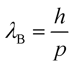 | (1) |
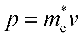 is the momentum of the electron and
  is the effective electron mass.4 Confinement in one dimension results in the formation of quantum wells, confinement in two dimensions forms quantum wires, and if a material is confined in all dimensions, quantum dots are formed. This affects the density of states (DoS) of the material, therefore changing its properties. The DoS of a system is the number of states an electron or hole can occupy at a certain energy per unit volume, and the DoS for different dimension systems can be seen in Fig. 2. For a bulk system, the DoS is a function of √E, meaning that above the conduction band energy EC, the density of states increases with energy.5 For a quantum well, the DoS does not depend on energy, which means above a certain energy, a significant number of states become available. For a quantum wire, the DoS is a function of E−1/2, meaning that the density of states decreases with energy. Another interpretation is that all the states up to the Fermi level are filled at 0 K.6 For a QD, the confinement is in all directions and the DoS is expressed as a delta function. This means that there are states available only at certain energies, which makes the levels discrete.7
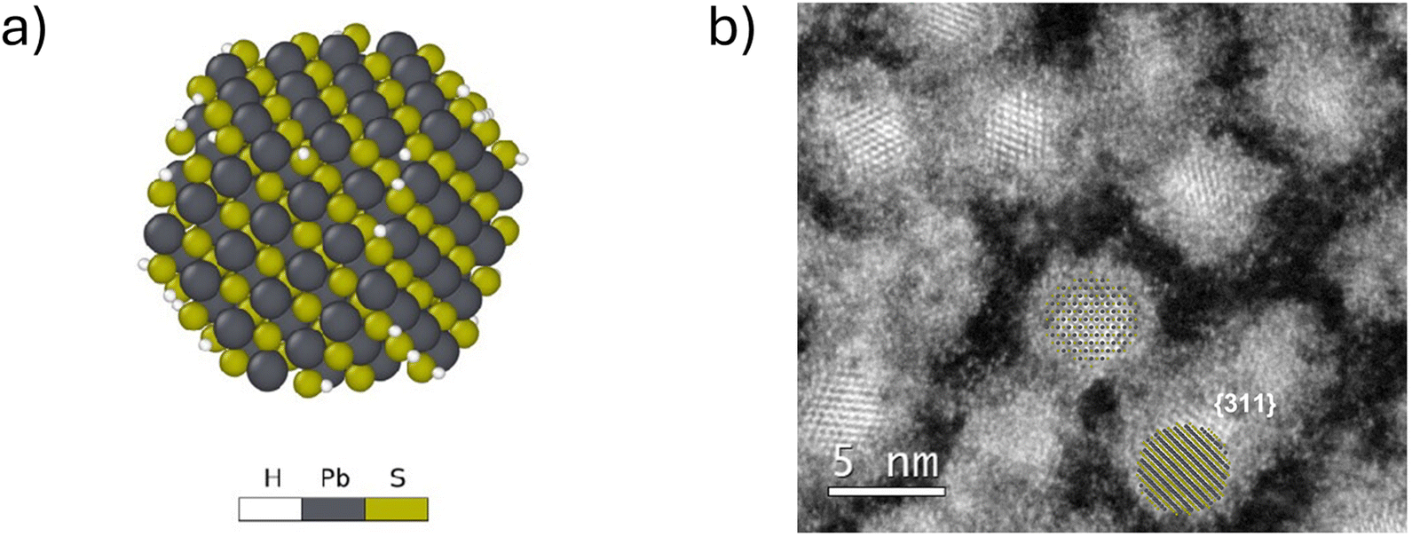 | ||
| Fig. 1 (a) Visualisation of a passivated sulfur-rich PbS QD and (b) high-resolution high-angle annular dark-field scanning transmission electron microscopy (HAADF-STEM) image of PbS QDs after cleaning with methanol.3 | ||
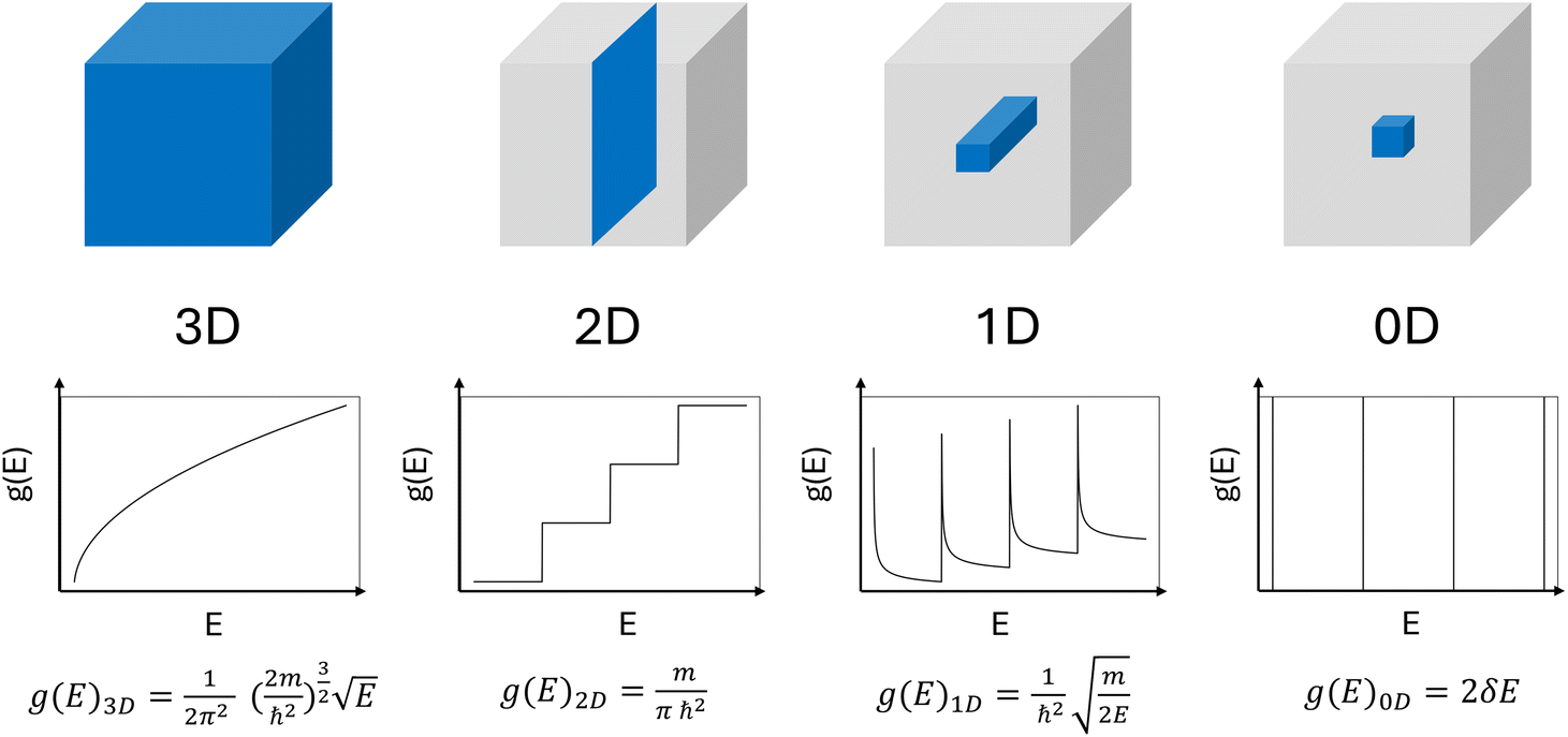 | ||
| Fig. 2 Showing the density of states for systems with different dimensions. | ||
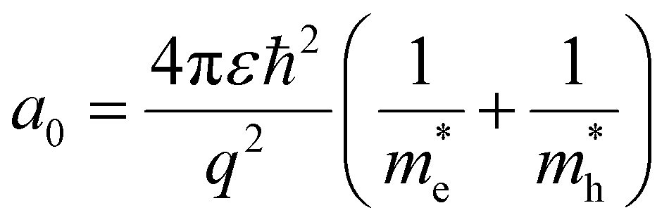
There are different levels of confinement regimes, which can be categorized depending on the size of the material in comparison with its exciton Bohr radius, given by
 | (2) |
 is the effective hole mass.8 The Bohr radius is defined as the distance between the bound electron and the hole. A strong confinement regime is when the material is smaller than the Bohr radius, a weak regime is when the material is larger than the Bohr radius, and an intermediate regime also exists, when the material is smaller than either the electron or hole Bohr radius, but larger than the remaining one. The Bohr radii for commonly used semiconductor and CQD materials are given in Table 1.
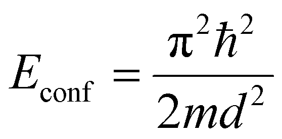
QDs are said to be zero-dimensional structures, as the charge carriers are trapped in all dimensions. In order to calculate the bandgap and energy levels of a QD, a couple of different factors need to be taken into account. The first one is the bandgap of the material itself in the bulk form. The second is the energy that results due to the confinement of the particles. This can be approximated by the energy levels of a “particle in a box”, which can be calculated by solving the time-independent Schrödinger equation. The result is given by
 | (3) |
 | (4) |
 | (5) |
From eqn (5), one can see that the energy levels of a QD are dependent on size, as well as their composition and shape. The composition of the QDs affects the bulk bandgap, along with the effective mass of the charge carriers, and the shape of the quantum dot dictates the energy resulting from the quantum confinement. The size plays an important role, as same shape and composition QDs can be made in different sizes to have varying optical properties. Larger QDs have smaller bandgaps and therefore absorb and emit in longer wavelengths. In contrast, smaller QDs have greater confinement and larger bandgaps and therefore absorb and emit in shorter wavelengths.
QDs can be made with different types of semiconducting materials. These can be II–VI, III–V and IV–IV group compound semiconductors. Perovskite materials have also been used to make QDs. The structure of the QDs can also differ depending on the application. The simplest QDs are formed as core structures, meaning that the nanocrystals have no shells around them. However, the dangling bonds and surface defects resulting from the high surface area to volume ratio will affect the luminance and QY of the QDs.20 Ligands have been proved to be effective in improving the surface structure of QDs by attaching to them and therefore improving the QY, optical properties, and stability.21 Even with these improvements, the stability and QY of the core QDs still suffer for commercial applications. A core–shell QD (CSQD) structure addresses this problem by passivating the surface and increasing the QY. In addition, it provides additional protection against environmental effects like oxidation and humidity, increasing stability.
CSQDs can be classified into 5 different groups depending on their bandgaps. These can be seen in Fig. 3. Type I CSQDs have the core's bandgap smaller than that of the shell, and the conduction band (CB) and the valence band (VB) edge of the shell are larger and smaller than the CB and the VB of the core, respectively. This allows for a better confinement of charge carriers in the core. Inverse Type I CSQDs have the opposite, where the shell has a smaller bandgap than the core, and the CB and VB edges of the shell are smaller and larger than that of the core band edges, respectively. This allows for the charge carriers to be more confined in the shell. In Type II CSQDs, the CB and VB edges of the shell are smaller than that of the core. This results in the electrons being more confined in the shell region and holes in the core region. On the other hand, in Inverse Type II CSQDs, the CB and VB edges of the shell are larger than that of the core, resulting in the electrons being more confined in the core and holes in the shell. In the Quasi-Type II CSQDs, the VB edge of the shell is smaller than that of the core, where the CB edge of the core and shell are quasi-aligned. As a result, the electrons are delocalized and the holes are mostly confined in the core.
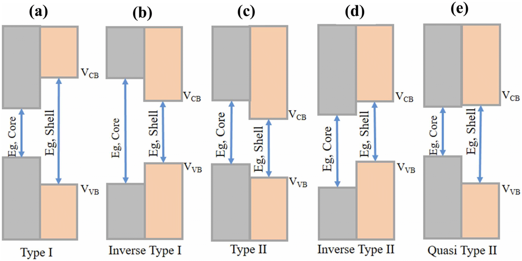 | ||
| Fig. 3 Different types of core–shell structured QDs classified based on their bandgaps and band alignments.22 | ||
Even though the theory for QDs was available and long known, there were a lot of question marks on whether it was possible to fabricate nanocrystals and use them in practice. This changed in 1981 when Ekimov et al. successfully grew multicomponent microcrystals inside silicate glass, and continued to publish 2 more works by 1985 extending the knowledge on the topic.23–25 The microcrystals were made of CdSe and CuCl, and it was shown how different temperatures can create a range of different sizes of microcrystals, going as small as 30 Å. A similar work was published by L. E. Brus and his team in 1983 where the Raman and electronic spectra of CdS crystallites (with a typical diameter of 45 Å) in aqueous solution were studied.26 Afterwards, in 1990, Bawendi et al. successfully bound organic moieties to CdSe nanocrystals, by reacting them with Se-phenyl. This made the crystals hydrophobic without altering their optical properties, which was the first time these crystals were manufactured in a “free-flowing” state.27 This paved the way for further improvement in 1993 when Murray, Norris and Bawendi successfully fabricated CdX (X = S, Se, Te) crystallites with their sizes ranging from 12 Å to 115 Å, and having size distributions <5% rms in diameter.28 This method is now commonly referred to as colloidal synthesis. For their work, Moungi G. Bawendi, Louis E. Brus and Alexei I. Ekimov were awarded the 2023 Nobel Prize in Chemistry for the discovery and synthesis of QDs.
3. Colloidal quantum dots
There are many different ways of synthesising QDs. They fall under two main categories: top-down methods and bottom-up methods. Top-down methods are wet-chemical etching, reactive ion beam and focused ion beam. These methods start with bulk materials and break them down into smaller nanocrystals to form the QDs. Bottom-up methods can be broken down into two groups: wet-chemical methods and vapour phase methods. These can further be broken down into different groups. Vapour phase methods are physical and chemical vapour depositions, and epitaxial growth (e.g. molecular beam epitaxy). Wet-chemical methods are aqueous synthesis and organometallic synthesis, which include colloidal synthesis.Colloidal synthesis is a solution-processed method. Metal ions, generally in organometallic compounds, are dissolved in solvents and treated both chemically and physically to synthesize the desired QDs with desired properties.29 CdSe QDs were one of the first to be synthesized with this method and therefore are one of the most studied. Murray, Norris and Bawendi's first proposed method used dimethylcadmium (Me2Cd) as the Cd precursor and tri-n-octylphosphine selenide (TOPSe) as the Se precursor, which were both dissolved in tri-n-octylphosphine (TOP). Tri-n-octylphosphine oxide (TOPO) was dried and degassed in a reaction vessel (often a flask) by heating and flushing with inert gas. The precursor solutions were mixed in a syringe in a glovebox. The heat from the flask was removed and the contents of the syringe inserted into the constantly stirred flask, in which a colour change could be rapidly observed. After the heat was dropped to a certain amount, it was restored. The time after the heat restoration, and the increasing and decreasing of the solution temperature dictates the size and the growth conditions of the crystals. The nanocrystals that form in solution can be isolated and purified with centrifugation. In this particular method, the solution was mixed with anhydrous methanol, anhydrous 1-butanol, and 2 more times with anhydrous methanol, each followed by a centrifugation. TOP/TOPO-capped CdSe was obtained after vacuum drying, and could be dispersed in different types of solvents (alkanes, alcohols, organic solvents etc.).
Me2Cd is extremely toxic. It can cause irritation to the respiratory system, it is a known carcinogen, and long-term exposure causes damage to internal organs. For these reasons, different Cd precursors have been tested to produce Cd-based QDs. Liu et al. in 2000 used Cd(ClO4)2 in mercaptoacetic acid as a Cd precursor and Na2SeSO3 as the Se precursor.30 The size distribution for this work was not reported, and the precursors used still had acute toxicity. In 2001, Peng et al. aimed to use less toxic and more scalable precursors and methods to synthesize CdSe QDs. The first precursor tested was CdCl2, which successfully created good-quality QDs. However, the Cd complex still had to be prepared separately, and the one-pot synthesis was not successful with this precursor. Therefore, another precursor, CdO, was tested, and successfully synthesized CdSe nanocrystals with a size distribution around 10%.31 Čapek et al. in 2009 used Cadmium Carboxylate (CdCAR) as the Cd precursor, mixing it with Hexadecylamine (HDA) and 2-octadecene (ODE) in a four-neck flask. The solution was degassed at room temperature followed by degassing at 100° under a nitrogen flow. Similar to the previous method, TOPSe dissolved in TOP was injected into the solution after the solution temperature was raised to the injection temperature. As before, <5% size dispersion in diameter was observed, and a PLQY of 93% was obtained.32 In early 2014, Hou et al. elucidated the fundamental radical reaction steps in the dissolution of elemental Se and S in non-coordination solvent 1-octadecene (1-ODE) and oleylamine with the view of facilitating the large-scale synthesis of CdSe QDs. They demonstrated that the radical-mediated solubilisation of Se can be significantly accelerated by the addition of azobisisobutyronitrile (AIBN), a common radical initiator used in the polymer industry.33
In addition to the CdSe QDs, PbS QDs also attracted a lot of attention. The main advantage of PbS QDs over CdSe QDs is the larger exciton Bohr radius (as seen in Table 1), allowing for confinement effects to be observed at larger dimensions. Furthermore, having a bulk bandgap of 0.41 eV has allowed the synthesis of PbS QDs with bandgaps ranging between 0.7–2.1 eV, making them very suitable for uses in photovoltaic applications.34,35 There are two main methods used to synthesize PbS QDs. The first method is the one-pot synthesis of dihydrolipoic acid (DHLA)-stabilised QDs.36 Initially, lipoic acid is reduced using excess sodium borohydride, producing aqueous DHLA. The DHLA solution pH is then adjusted to 9 by the addition of NaOH. Lead(II) Acetate (PbAc2) solution is then inserted into the solution with strong magnetic stirring, followed by the addition of Na2S by drops. The colour change of the solution to dark brown indicates the formation of PbS QDs, and the process takes less than 30 min. The second method uses a Schlenk line and widely reported materials: octadecene (ODE) as the noncoordinating solvent, oleic acid (OA) as the ligand, PbO as the lead source and bis(trimethylsilyl)sulfide [(TMS)2S] as the sulfur source.37,38 PbO and OA are mixed in ODE, degassed and heated up to 100 °C under vacuum to dry the solution and form lead oleate. Depending on the injection temperature, the solution is then heated or cooled down, followed by the injection of (TMS)2S in ODE. The temperature is kept constant for the reaction time and then quenched by pouring isopropanol. Similar to CdSe, centrifugation processes were used to separate and collect the QDs afterwards.
Even though there have been many advances in Cd and Pb-based QD synthesis, the Restriction of Hazardous Substances Directive has limited the use of heavy metals in electric and electronic applications due to their toxicity. Even though this restriction does not apply to solar cells (which is the main application of PbS QDs), a lot of effort has been made to produce heavy metal-free QDs to replace toxic elements. Some promising candidates include InP,39,40 carbon,41 CuInS2,42 and perovskite,43 which have achieved near unity PLQYs, and others like SnSe,44 silicon,45 CuGaAlS,46 CuInZnS47 which have achieved relatively high PLQYs (60–90%) and high quantum efficiencies. This was possible by using different combinations of core–shell or core–shell–shell structures as discussed in the previous section. InP, in particular, has attracted a lot of attention due to the wide spectral tunability, strong absorption, high carrier mobility and effective luminescence.48 It has been one of the most promising heavy-metal-free CQDs. As expected, there are a couple of different ways of synthesizing InP QDs, using similar methods described above for CdSe and PbS CQDs. One of the two48 main synthesis methods involves reacting Indium(III) alkanoates [In(RCOO)3, where R is an alkylic chain] with organic silyl phosphine [P(SiR3)3, where R is an alkyl, most often methyl] with temperatures reaching up to 300 °C. This produces CQDs capped by alkanoates. There are a couple of issues with this method, due to the side reactions that take place, which might in turn affect the final product of the synthesis. Furthermore, the silyl phosphine precursors are pyrophoric, which is hard to handle and a higher-risk chemical to use overall. The second method is reacting Indium(III) halides (most often InCl3) with aminophosphines. This method produces QDs capped with halide ions and alkylamines. The second method is less used and studied but is cost-attractive due to the cheaper precursors.
4. Internet of things
4.1. What is the internet of things?
The term “IoT” was first used and published in 1985 by Peter T. Lewis, but was popularized by Kevin Ashton in 1999. IoT describes an infrastructure, which enables advanced services by interconnecting physical and virtual “things” based on the continuously evolving technologies for information and communication. A thing for IoT can be described as an object of the physical world (physical) or the information world (virtual) that can be integrated into networks and can be identified separately.49 One of the first academic papers that envisioned the concept of IoT was published by Mark Weiser in 1991.50 He mentions the use of hundreds of computers and devices in a single room and even compares the scariness of this to the scariness of carrying hundreds of volts inside walls when electricity was first implemented into our daily lives. He adds to this with “People will simply use them unconsciously to accomplish everyday tasks”. Since the publishing of his paper, a lot of improvements have been made in terms of technology and wireless communication. In 2003, when the world population was 6.3 billion, there were about 500 million devices connected to the internet. This gives a ratio of devices connected to the internet to the world population of about 0.08. In 2010, this ratio increased to 1.84, with the world population being 6.8 billion and the number of devices connected to the internet being 12.5 billion. Sometime between 2003 and 2010, this ratio surpassed 1, which is interpreted by Evans as the time IoT started to exist.51 Some of the many potential applications of IoT are shown in Fig. 4.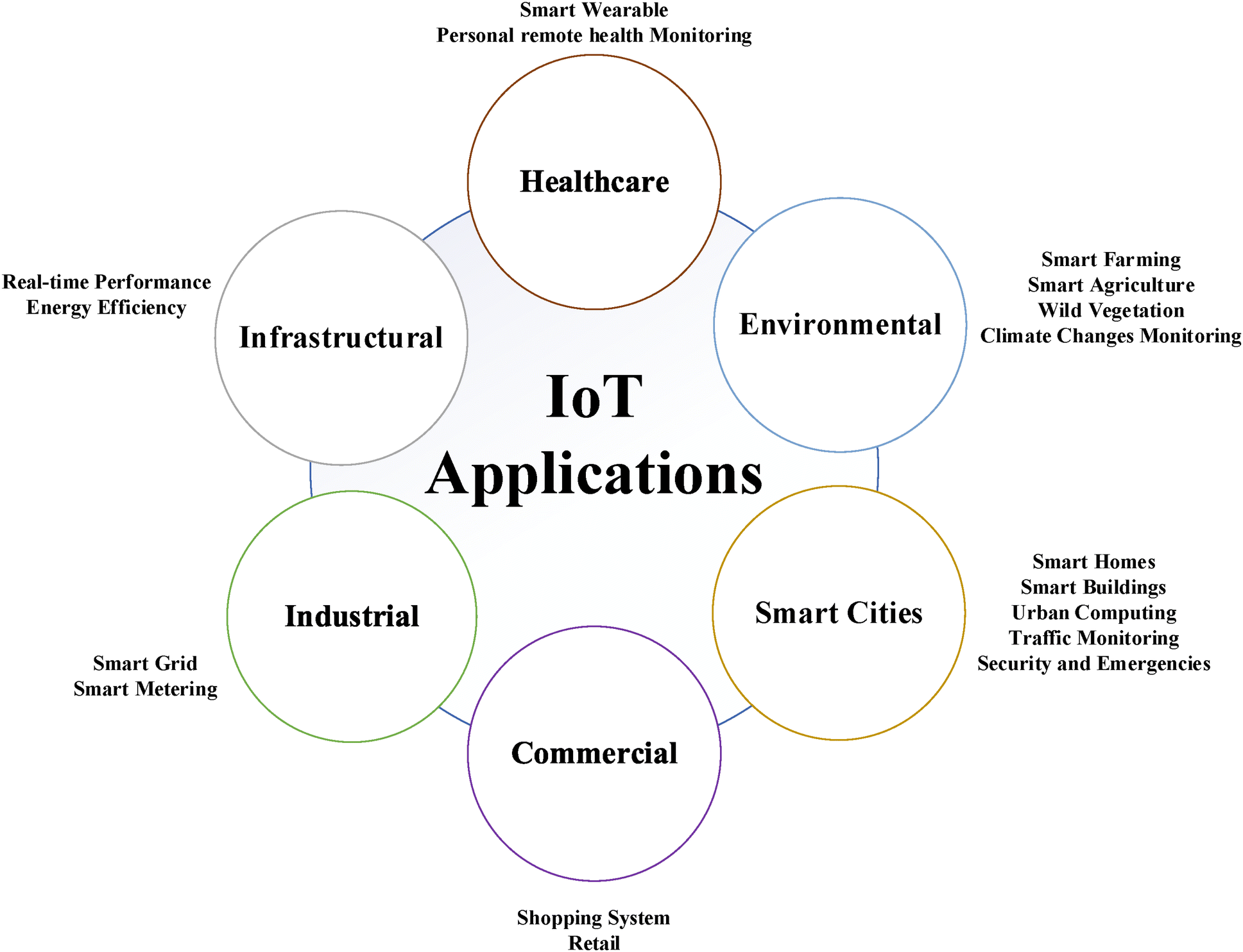 | ||
| Fig. 4 Different applications of IoT categorized into 6 main categories.52 | ||
In order to understand how IoT works, we have to first understand some key computing concepts. Cloud computing can be defined as a computing method where lots of low-cost computing units connected by IP networks are used to provide IT services.53 It is a metaphor for the internet, as it “looks over everything else”, kind of like a cloud in the sky. Cloud computing works by collecting data over a shared data centre which has the security, storage and power capacity, rather than doing things locally. There are many advantages to cloud computing, especially when it comes to storage, since access can be gained anywhere where a connection can be made to the data centre, i.e. via the internet. However, it is not always advantageous to use cloud computing, especially in situations where a fast response is necessary. Fog computing addresses this issue by processing closer to the devices and sensors, while having connections with the storage and network capabilities of the cloud. Fog computing is often described as dense architectures at the network's edge.54 The name comes due to the fog appearing nearer to the Earth's surface, similar to how fog computing operates nearer to the edge of the network. Even though it has been successful in addressing some problems with cloud computing, there are still drawbacks of fog computing due to communication from devices/sensors, power usage, bandwidth etc. This led to the concept of mist computing, which is at the edge of the computing network. Mist computing aims to make devices and sensors more independent of the cloud network so that they can communicate and solve problems even if there is a failure to connect to the cloud.55 It is important to understand that this does not mean that mist computing is aimed to be used without the need for cloud or fog computing. Each of these methods has its advantages and disadvantages, and are proposed so that they can work together to maximise the strengths and minimise the weaknesses. A representation of a communication network is shown in Fig. 5. It can be seen that the core of the architecture is the cloud, where the computational power, data storage and bandwidth are the highest. As you move from the core towards the edge, the responsivity and mobility of the devices increase, as well as their cost and latency. The edge layer shown in the figure represents the mist layer. However, the name “edge layer” has been used to represent the fog layer in the past, and so the use of “mist layer” makes it easier to distinguish between the different types of computing methods.
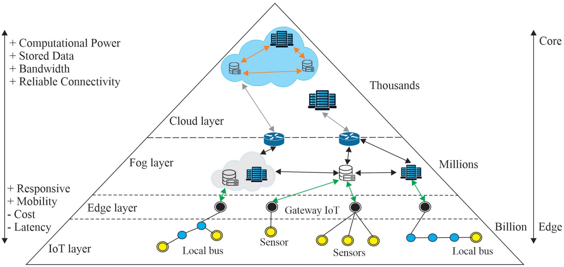 | ||
| Fig. 5 Showing the different layers of the network, starting from the central cloud layer out into the edge and IoT layers. PERMISSION.56 | ||
The devices on the edge layer need different components to be able to communicate with each other. The general demands for the devices are to be low cost and producible on a large scale. The demand for low carbon footprint devices has also increased due to the net zero initiative many companies and countries are aiming for. In addition, with the rapid development of technologies, new applications are emerging that require flexible and transparent devices/components. The main components required for a smart IoT device to communicate with the rest of the network are:
• Switches
• Emitter
• Receiver
• Power source
The emitter and receiver are required to send and receive data, as their name suggests. Switches are required to control the current flow to or from these components. A power source is required to supply the power required for the devices to run. CQDs have proved their potential in this area due to their properties and can be implemented in these devices. The next section will aim to give information on the possible devices that can be used for these components.
4.2. Colloidal quantum dot internet of things devices
After the successful synthesis and demonstration of CQDs, the community was quick to start thinking of applications that could make use of these nanocrystals. However, unlike the bulk, the characterization of processes on the nanoscale was not well understood then. It was important to try and fill the gaps in the literature to overcome problems that might arise from the emerging applications of CQDs later down the road. Kagan et al. in 1996 used PL measurements to understand electronic energy transfer in CdSe CQD solids.57 Two different size CQDs were synthesized and their PL measurements were done separately in solution and as film. Then a solution and film of 18% large dots and 82% small dots were prepared and compared with their pure spectra. Comparison of QYs showed quenching of the small dots’ emission and enhancement of the large dots’ emission in the mixed film. Time-resolved PL also showed a decrease in the small dot PL lifetime and an increase in the large dot PL lifetime in the mixed film, indicating electron energy transfer from small to large dots. The authors then confirm that long-range resonance transfer (LRRT) leads to electronic energy transfer in close-packed QDs. Wang et al. did another study in 2001 to see the effects of an electrochemical potential on CdSe QDs.58 IR and Visible spectra obtained in their experiment showed direct evidence that the electrons are injected into the 1S state of the QDs. Applying a potential induces quenching that was visible to the eye. It was deduced that the IR absorption was solely dependent on the 1s electrons, whereas the PL could be strongly quenched by the charges in the surface band-gap states. This was an important finding indicating the importance of surface passivation in CQDs. Another work published by the same group in 2003 showed that with potassium or electrochemical doping, it is possible to increase the occupation of the 1s and 1p shells in CdSe nanocrystals and increase the conductivity of QD thin films significantly.59 Kagan et al. in 2003 talked about the needs and rules for achieving Self-Assembled Monolayer Field-Effect Transistors (SAMFETs).60 It was stated that new synthesis methods that will make separation of byproducts easier are necessary for reducing impurities that might dominate electrical characteristics, and characterization must be done at the molecular level to understand the origin of charge transport in devices. Kovalenko et al. in 2009 used metal chalcogenide complexes (MCCs) as surface ligands on CdSe CQDs as a replacement for the conventional organic ligands, and controlled the conductivity of films by controlling the ratio of MCCs to CQDs.61 Scheele et al. published a work in 2011 on the thermoelectric properties of lead chalcogenide core–shell nanostructures, showing a p-type to n-type transformation on PbTe–PbSe due to thermally induced alloying.62 Works like these paved the way for understanding charge transfer at the molecular and nanoscale, which paved the way for future research on CQD devices.The main difference between TFTs and other FETs is that the semiconducting layers are deposited as a thin film. The quality of the deposited films is generally lower compared with other types of transistors, hence the mobility is generally smaller. However, the main advantages of TFTs are that they have simpler structures, meaning they can be manufactured in fewer steps and at lower cost. The different structures used for TFTs can be seen in Fig. 6. They consume less power, have quicker reaction times and have higher, more accurate response rates. For these reasons, they were the preferred type of transistors for display applications. These properties make them suitable for use in IoT devices as well.
 | ||
| Fig. 6 Different structures of a TFT. (a) Bottom-gate staggered. (b) Bottom-gate coplanar. (c) Top-gate staggered. (d) Top-gate coplanar.68 | ||
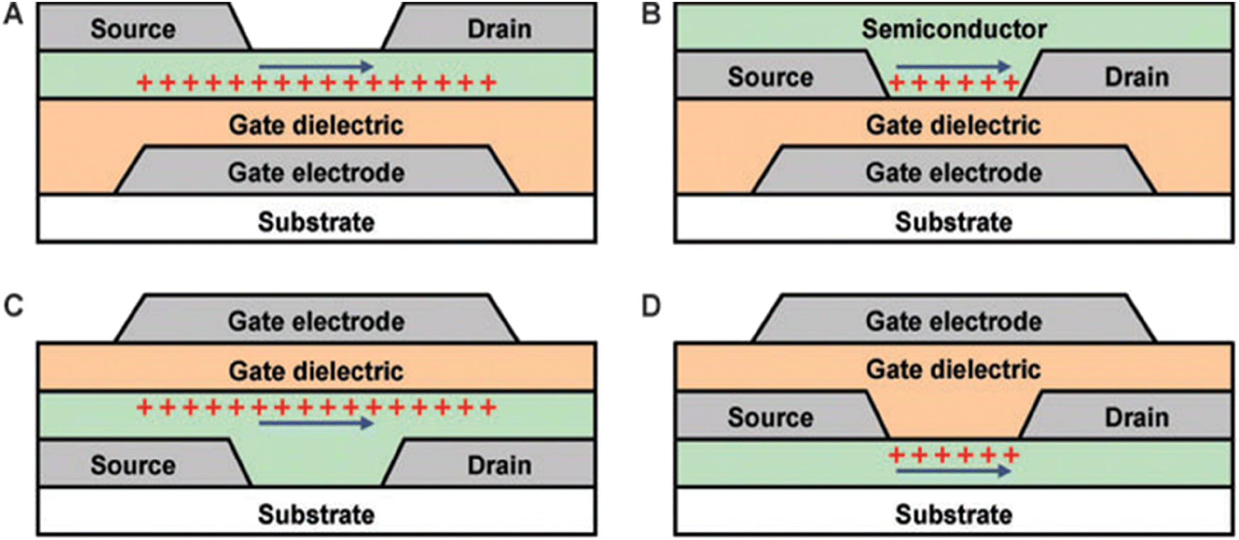
Different materials have been researched for their use in TFTs. In 1964, Klasens and Koelmans used SnO2 as the semiconducting layer.69 Just 4 years after that, Boesen and Jacobs used Lithium-doped ZnO as the semiconducting layer.70 These were the first metal-oxide-based TFTs. However, they were fabricated using vacuum-based methods like evaporation, which were costly. In addition, there were problems with their performances, like poor modulation and no saturation of the drain current. However, in the late 1970s, LeComber et al. successfully fabricated a TFT using a-Si.71 This was a major breakthrough in TFT technology due to the rapid popularity silicon was gaining as part of the digital revolution. Following this, a TFT using poly-Si was fabricated. Eventually, Si-based TFTs were the first ones to be commercialized, in display applications. The next promising material for TFTs was organic semiconductors as the channel layer. The main advantage of organic TFTs (OTFTs) was their solution-processed nature, which simplified the fabrication process and decreased the costs. The topic of metal oxides being used as channel layers for TFTs came back into the conversation when 3 different fully transparent ZnO-based TFTs were fabricated by Carcia et al.,72 Masuda et al.73 and Hoffman et al.,74 which used rf magnetron sputtering, pulsed laser deposition and ion beam sputtering to deposit the channel layers, respectively. This was shortly followed by solution-based metal oxide channels. In 2005, Talapin et al. achieved both n-type and p-type channel field-effect transistors (FETs) from PbSe nanocrystal films by treating with hydrazine for n-type, and then desorbing hydrazine using vacuum or mild heating techniques, showing the possibility of using CQDs as different types of channel layers in FETs.75
When a potential difference is applied between the source and the drain and the source and the gate, the current flow between the source and the drain is given by
 | (6) |
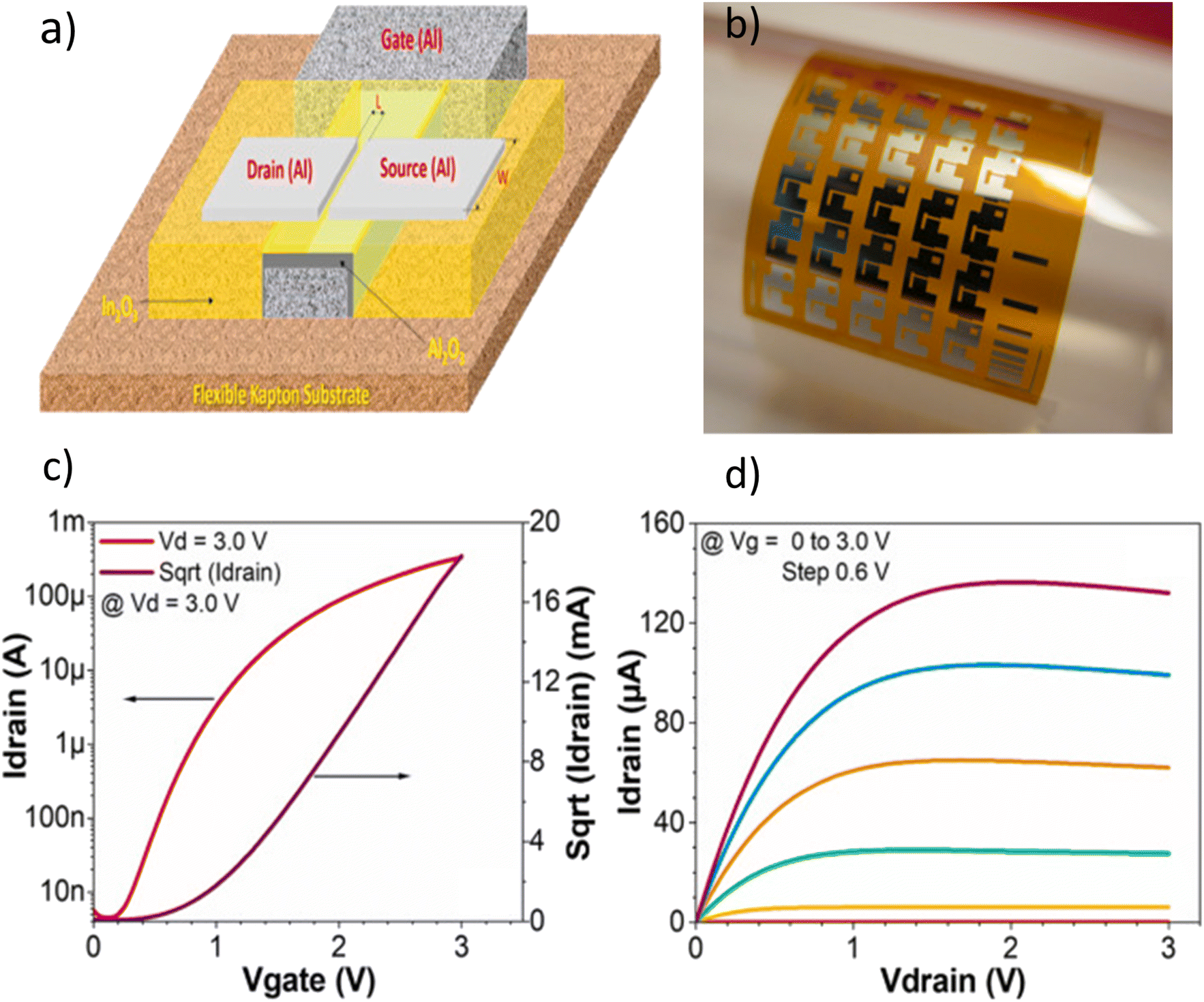 | ||
| Fig. 7 (a) The structure of an In2O3 flexible TFT on a flexible substrate. (b) A camera image of the TFTs. The (c) ID–VG and (d) ID–VD graphs of the TFTs.76 | ||
Field-effect mobility. Carrier mobility measures how fast charge carriers can move through a material. Different types of mobility measurements can be done on semiconductors, including Hall mobility, terahertz mobility, optical mobility etc. In the case of transistors, the mobility is obtained from a field-effect measurement, hence the name. Two different types of field-effect mobility can be measured: linear region mobility and saturation mode mobility. Linear region mobility is generally useful for amplification uses as the drain current is amplified in this region. It is given by the equation
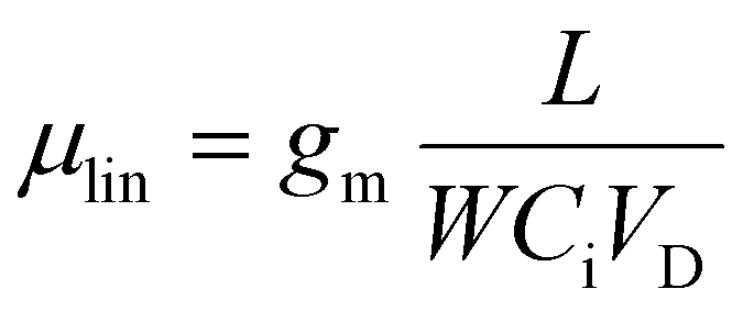 | (7) |
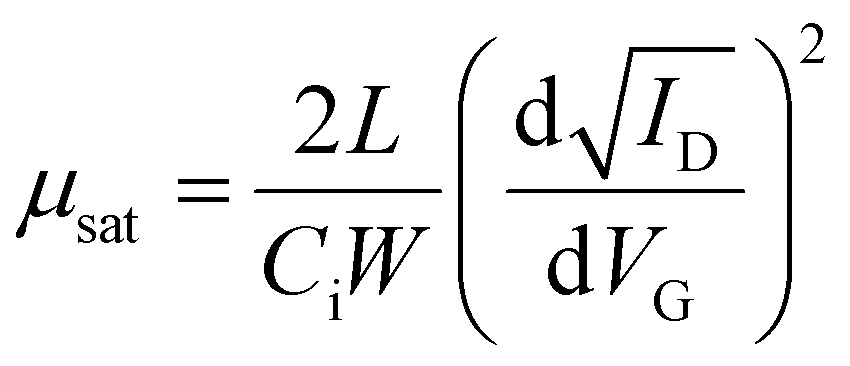 | (8) |
Sub-threshold swing. Sub-threshold Swing (SS) is a FoM that measures the performance of FETs in the sub-threshold region. It is a measure of how much VG is required to increase ID by one decade,77 and is given by
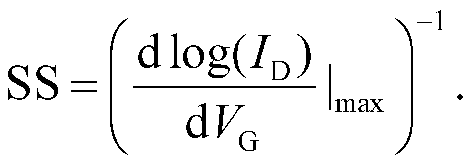 | (9) |
Threshold voltage. V T is another important parameter when characterizing any type of transistor. For a TFT, VT is the minimum VG required for the transistor channel to start conducting. VT can be experimentally obtained by measuring ID for a varying VG while keeping VD constant. This allows one to observe the change in the drain current with the increase of VG. VT in this situation can be defined as the VG where the slope of the transfer curve starts to change significantly, meaning that the current flow is increasing with the increase of VG.
On–off ratio. The on–off ratio is one of the most important parameters for not only TFTs but any type of transistor. In physical terms, it is the ratio of the ID when the device is turned on to the ID when the device is turned off. It can also be defined as the ratio of the maximum ID obtained when the device is saturated to the minimum ID. By definition, it is the ability of the device to switch from on to off states, and the distinctiveness of these states from each other. Generally, high on/off ratios are required for commercial applications.
State-of-the-art. The most common application of TFTs is in displays, both in passive and active matrix addressing methods. Based on its abundance and knowledge about its processing, Si is the most used material for channel layers of TFTs commercially. Amorphous (a:Si) and polycrystalline (p:Si) are the two different types used in TFT manufacturing. However, a:Si suffers from low mobility due to defects (0.5–1 cm2 V−1 s−1),79 and p:Si suffers from higher costs and difficulties in large-scale manufacturing. In addition, Si is not suitable for flexible and transparent electronics, which are becoming important properties for materials due to evolving applications.
Due to the limitations of Si, different materials have been researched in the past years. Some papers published in recent years using different materials as channel layers are shown in Table 2. It is important to note that the performances shown are not only dependent on the channel material but also dependent on the other structural properties including the W/L ratio, dielectric thickness, dielectric material etc. However, they are good indications of how far the research has improved and the potential of the materials. One can see that high mobilities can be obtained with both deposition methods and solution-processed methods. There is generally a trade-off between different FoMs, i.e. spin-coated IGZO has the highest mobilities but has quite low on/off ratios. The use of CQDs in TFTs has been challenging, due to the typically low carrier mobilities ranging around 10−4–1 cm2 V−1 s−1. Mobilities and on/off ratios reaching 27 cm2 V−1 s−1 and 106, respectively, were achieved in 2012 using CdSe CQDs; however, this has not been the case so far for heavy metal-free CQDs.80 On the other hand, CQDs have been proved to be more efficient when combined with another channel layer, where the absorption properties of a CQD can be combined with the TFT. This is discussed in more detail in the next section.
| Material | Process | Mobility (cm2 V−1 s−1) | SS (V dec−1) | Threshold voltage (V) | On–off ratio | Ref. |
|---|---|---|---|---|---|---|
| IGZO | Sputter | 7.78 | 0.27 | 1.34 | 107 | 81 |
| Organic C10-DNTT | Thermal deposition | 2.4 | 0.32 | −1 to −1.5 | >104 | 82 |
| IGO | Sputter | 78.73 | 0.147 | −1.07 | >108 | 83 |
| MoS2 | Wet transfer | 52.8 | 0.226 | −1 | 1.5 × 10⁸ | 84 |
| IGZO | Spin coat | 85 | 0.14 | ∼−0.3 | >104 | 85 |
| In2O3 | Spin coat | 9.17 | 0.105 | 1.38 | 108 | 86 |
| Organic C8-BTBT | Spin coat | 18.3 | — | −4 | 105 | 87 |
| CuInSe2 QDs | Spin coat | 0.7 | — | <5 | 104 | 88 |
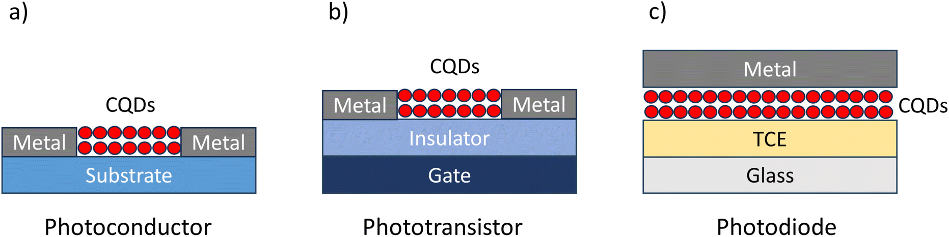 | ||
| Fig. 8 Structures of different types of CQD photodetectors: (a) a photoconductor, (b) a phototransistor and (c) a photodiode (TCE = transparent conductive electrode). | ||
The first phototransistor was announced by Bell Laboratories in 1950.90 It was developed by John Shive, and he proposed that instead of an electrical signal generating the charges, light absorption could be used. He introduced the concept of a new photoconductivity cell called the “Phototransistor”. The structure of this device differed from the transistor devices then available. The shape of the device is cylindrical, where pill-shaped germanium with a dimple on one side is secured with a retaining ring into a metal cartridge. The “collector” electrode is a pointed wire in the centre of the dimple. The device operation depends on the light absorption of the germanium between the collector and the peripheral contact, which increases the carrier concentration and decreases resistance. One of, if not the, first field effect phototransistors (FEPTs) was reported in 1960 by Bockemuehl, 10 years after the announcement of the original phototransistor.91 Bockemuehl was aiming to show the potential of II–VI materials, particularly in photoelectric applications, in comparison with III–V materials which were already utilised in transistors at that time. He made a device with a CdS channel, a drain and source electrode on each side, and a Cu gate deposited at the top. He first studied the Source–Drain characteristics with different gate voltages and then studied the current increase with different wavelengths of light. This work was one of the inspirations for Weimer that led to the discovery of the CdSe and CdS TFT in 1962. Weimer even included tests in the dark and under illumination as a comparison for the TFT performance, which showed amplification due to light. Modern FEPTs generally implement a bottom gate TFT structure and expose the channel to incoming light. Another possibility is to cover the channel with a more light-sensitive material to allow better light absorption. Due to the similar working principle, the FoMs of FEPTs are similar to the ones of TFTs, with additional ones that are used to understand and compare the light-absorption aspects.
Photoresponsivity. The first FoM to mention is the photoresponsivity, given by the equation92
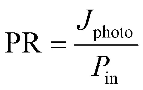 | (10) |
Photosensitivity. Another FoM for phototransistors is the photosensitivity P, given by95
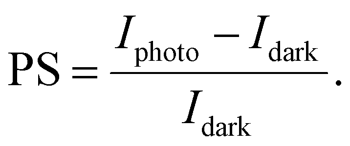 | (11) |
Specific detectivity. The specific detectivity (D*) is a measure of the weakening of the detection of light. It can be calculated from the PR, device area and noise level, and is given by96
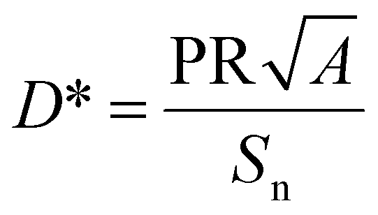 | (12) |
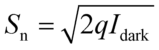 , assuming that shot noise is dominant.
External quantum efficiency. The external quantum efficiency (EQE) of a phototransistor can be defined as the number of charge carriers detected to the number of photons that are incident on the active area of the device. It can be calculated using92
 | (13) |
State-of-the-art. FEPTs have great potential in future IoT applications, since they bring together properties of two different devices, and can save space when integrating with other devices. Different structures are used to make FEPTs. As mentioned in the section above, some structures use a photoactive channel layer whose resistance decreases when illuminated with light, while others try and implement photoactive layers on top of more conventional channel layers used in TFTs. Examples of this can be seen in Fig. 9(a) and (d), where a PbS and perovskite QDs as active layers are used on MoS2 and IGZO channel layers, respectively. However, there are inconsistencies when reporting phototransistor characteristics and FoMs, due to their different applications. Different works report more of the transistor FoMs, which are mentioned in the previous section, due to the device properties being more fit for switching applications. The transfer curve for the PbS CQDsMoS2 FEPTs can be seen in Fig. 9(b) with the output curves shown in the inset. The output curve at different illumination levels can also be seen in Fig. 9(c). On the other hand, others report more on the light-detection FoMs. The PR-VG graph of the perovskite QD/IGZO FEPT can be seen in Fig. 9(e). Even then, not all works report all FoMs, as seen in Table 3. The mobility for the devices is sometimes reported as the mobility of the FEPTs, whereas sometimes the mobility of TFT without the active layer is reported, assuming that the properties of the channel will be similar. Different ranges of operation wavelengths can be obtained by changing the active layer of the devices. The highest PR is obtained with heavy-metal-based QDs, although InP-based FEPTs have been reported with an order of magnitude smaller PR. However, CdSe-based FEPTs show a very high D*, 4 orders of magnitude higher than perovskite-based FEPTs. There are reported works on using FEPTs in arrays for use as sensors. Bala et al. in 2022 demonstrated a 7 × 7 array of MoS2 transistors that can be used as transparent image sensors.97 Chen et al. in 2024 showed the use of a CQD-sensitized IGZO phototransistor array for neuromorphic vision sensors.98
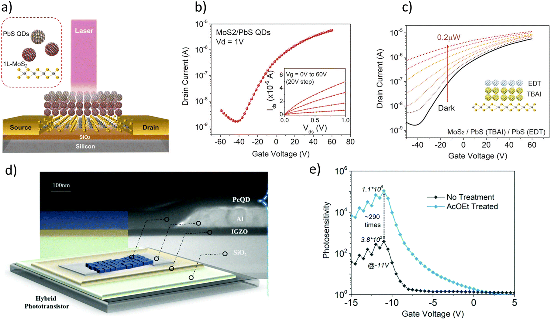 | ||
| Fig. 9 (a) The structure of a PbS/MoS2 phototransistor, its respective (b) ID–VG graph (inset: ID–VD for different VG) and (c) ID–VG graph at different illumination powers.93 (d) The structure of hybrid perovskite QD and its (e) PR-VGS graph.94 | ||
| Material (active/channel) | Process | μ (cm2 V−1 s−1) | PR (A W−1) | PS | D* (J) | Wavelength (nm) | Ref. |
|---|---|---|---|---|---|---|---|
| CsPbBr3 QDs/ZnO | Spin coat/spray pyrolysis | 21.81 | 567 | 107 | 6.59 × 10¹³ | 520 | 99 |
| PbS QDs/MoS2 | Spin coat/CVD | 3.4 | 5.4 × 10⁴ | — | 1011 | 850 | 93 |
| CdSe QDs/a-IGZO | Spin coat | 15.48 | 1.1 × 10⁴ | — | 5.3 × 10¹⁷ | 520 | 100 |
| P3HT:HgTe QDs | Spin coat | 5 × 10⁻⁴ | >1 | — | >1011 | <2250 | 101 |
| HgTe QDs with As2S3 | Drop-cast | 10−2 | 0.1 | — | 3.5 × 10¹⁰ | 3500 | 102 |
| MoS2 | Sputtering | — | 27 | 364 | 3.5 × 10⁸ | 405 | 97 |
| PbS-I/IGZO | Spin coat/sputtering | 8.6 | 45.3 | — | 9.3 × 10¹² | 1064 | 103 |
| InP/MoS2 | Spin coat/wet transfer | — | 1.3 × 10³ | — | — | 532 | 104 |
The main advantage of OLEDs over other display technologies is that they can be made into an active matrix. This allows individual pixels to be addressed with the use of transistors and capacitors, decreasing power consumption and increasing refresh rates. However, the main disadvantage of OLEDs is the problems with the device lifetime, owing to the poor stability of organic materials. For display applications, around 20![[thin space (1/6-em)]](https://www.rsc.org/images/entities/char_2009.gif) 000 h of lifetimes is required with brightness levels of around 100 cd m2.116 However, the brightness of OLEDs drops especially when used at high luminance. The three mechanisms responsible for this are dark spot degradation, catastrophic film failure and intrinsic degradation.117 For these reasons, research into alternatives to replace organic materials for emitters grew. Perovskite materials and CQDs showed promising results for use as emitters in layer-stacked LEDs. Even though perovskite LEDs (PeLEDs) have reached EQEs of higher than 20% for green, red and NIR wavelengths, they suffer from loss of EQE at high current densities, short lifetimes, poor efficiencies in blue-emitting devices and access to greater than 800 nm of peak wavelength due to bandgap restrictions.118 CQDs have also reached EQEs higher than 20% for red and green-emitting devices, while also having lifetimes that can reach up to 1000000 h, being comparable to or even better than commercial OLEDs.119,120 The FoMs of QLEDs are shared with OLEDs and PeLEDs, as they share similar structures and applications.
000 h of lifetimes is required with brightness levels of around 100 cd m2.116 However, the brightness of OLEDs drops especially when used at high luminance. The three mechanisms responsible for this are dark spot degradation, catastrophic film failure and intrinsic degradation.117 For these reasons, research into alternatives to replace organic materials for emitters grew. Perovskite materials and CQDs showed promising results for use as emitters in layer-stacked LEDs. Even though perovskite LEDs (PeLEDs) have reached EQEs of higher than 20% for green, red and NIR wavelengths, they suffer from loss of EQE at high current densities, short lifetimes, poor efficiencies in blue-emitting devices and access to greater than 800 nm of peak wavelength due to bandgap restrictions.118 CQDs have also reached EQEs higher than 20% for red and green-emitting devices, while also having lifetimes that can reach up to 1000000 h, being comparable to or even better than commercial OLEDs.119,120 The FoMs of QLEDs are shared with OLEDs and PeLEDs, as they share similar structures and applications.
External quantum efficiency. EQE is one of the biggest limitations of layer-stacked LEDs. It is defined as the number of photons that make their way out of the device to the number of electron–hole pairs that are injected into the device. It can be measured by measuring the power output of a device, most often done by using an integrating sphere, and then using the equation122
 | (14) |
| ηext = LEE × ηint = LEE × qeff × ηS/T × γ | (15) |
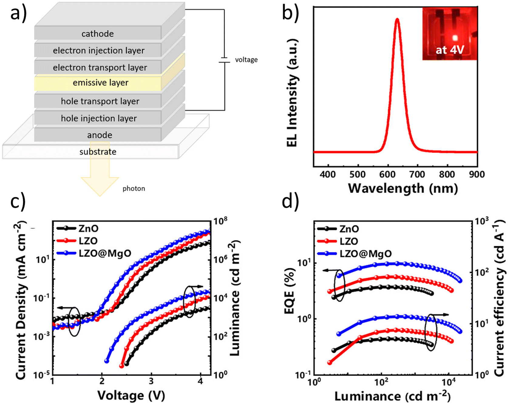 | ||
| Fig. 10 (a) The general structure of QLEDs. (b) The EL spectra and the (c) CD–V–L and (d) EQE–L–CE graphs of an InP-based QLED with different ETLs.121 | ||
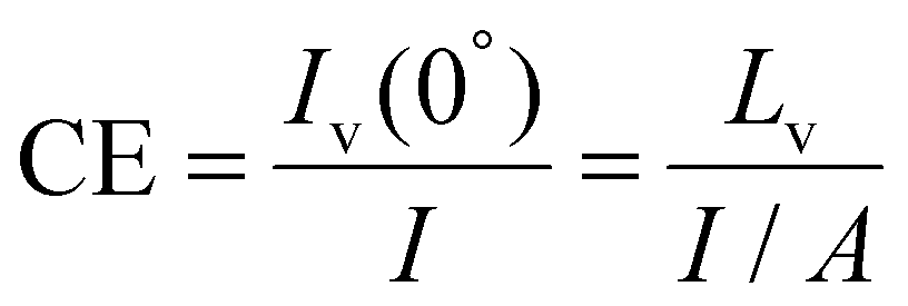
Current efficiency. Current Efficiency (CE) is another important parameter for QLEDs. It can be defined as the luminous intensity in the normal direction to the device (Iv(0°), luminous flux per solid angle) divided by the input current. It can also be calculated by dividing the luminance Lv (luminous intensity per area), by the current density125
 | (16) |
Turn-on voltage. The turn-on voltage is the voltage at which the device reaches a luminance of 1 m−2.126 It is an important parameter since generally the lower the turn-on voltage, the lower the range of operation voltages, and hence lower power consumption.
Lifetime. Lifetime is an important parameter for QLEDs and is different for various applications. For display applications, a lifetime of >10
000 h is required.127 There are different factors that affect QLED lifetimes. These include PL quenching, non-radiative recombination mechanisms (e.g. Auger recombination), Förster resonance energy transfer, and efficiency drops at high currents.128
State-of-the-art. QDs have been commercialized in display applications under the name of “QLED” technology. However, this technology makes use of the PL properties of QDs, unlike OLED technology which uses EL mode emission. In commercialised QLEDs (CmQLEDs), the QDs are placed as a layer in the LCD sandwich. They absorb the blue backlight and emit it in their respective colours. The light then passes through filters to produce the desired colour on the screen. It is essentially LCD technology, with the performance being enhanced by the PL characteristics of QDs. The difference in the structures can be seen in Fig. 11. In comparison with CmQLEDs, OLEDs have better contrast, due to being able to switch light emitters completely to achieve better blacks. In addition, OLEDs generally have better uniformity and viewing angles in comparison with CmQLEDs, due to the nature of the backlight operation. However, CmQLEDs have brighter and more distinct colours in comparison with OLEDs. QLEDs mentioned in this section use the EL properties of QDs, which means that they can be made into AM structures just like an OLED. This means that in theory, QLEDs will have all the advantages an OLED has over a CmQLED, in addition to having brighter, more distinct colours and potentially longer lifetimes. The best-performing QLEDs in the past decades have been CdSe based, which were somewhat comparable to the performance of OLEDs. However, as mentioned in section 3, the use of Cd-based products has been banned due to the toxicity of Cd, which slowed down the process of commercializing QLEDs. Table 4 shows examples of recently published papers on red, blue and green-emitting OLEDs, CdSe-based QLEDs and heavy-metal-free QLEDs. Examples of a typical red EL emission, CD–V–L and EQE–L–CE graphs can be seen in Fig. 10(b), (c) and (d), respectively.
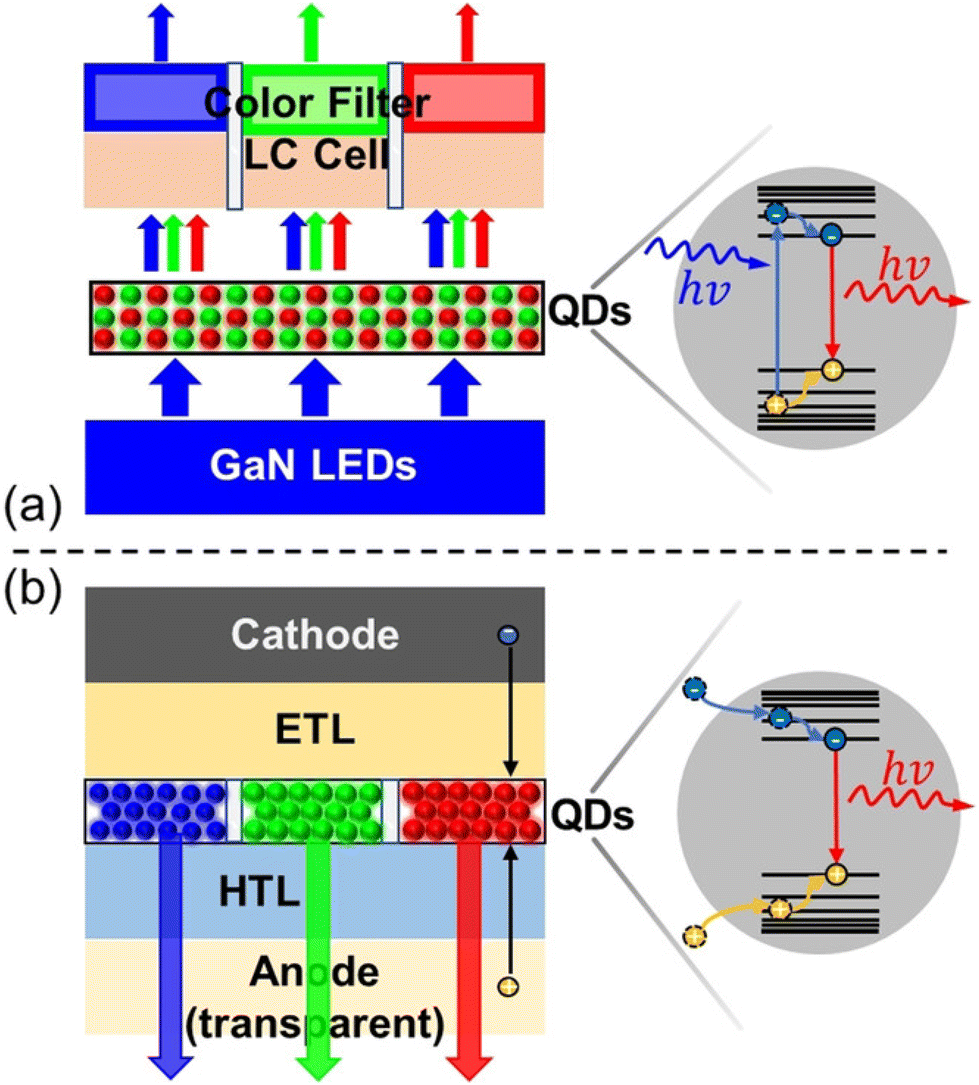 | ||
| Fig. 11 (a) The simplified structure of PL mode commercialised QLED TVs and their emission mechanism. (b) Structure of EL mode QLEDs and their emission mechanism. PERMISSION.129 | ||
| Material | Process | EQE (%) | CE (cd A−1) | Turn-on voltage (V) | Wavelength (nm) | Ref. |
|---|---|---|---|---|---|---|
| InP/ZnSe/ZnS QDs | Spin coat | 21.4 | — | 1.8 | 630 | 40 |
| CdZnSe/CdZnS/ZnS QDs | Spin coat | 30 | 38.7 | 1.8 | 628 | 130 |
| Organic 2SPAC-DBP-2tBuCz | Spin coat | 23.7 | 38.6 | 2.3 | 583 | 131 |
| InP/ZnSe/ZnS | Spin coat | 16.3 | 57.5 | 2.2 | 545 | 132 |
| CdSeZnS/ZnS/ZnS | Spin coat | 25.04 | 96.42 | >3 | 524 | 128 |
| Organic BCC-36:PO-T2T(5:1) + 12.5%Ir(ppy)2(acac) | Spin coat | 32.5 | 50 | 3.5 | ∼520 | 133 |
| CdSe/ZnS | Spin coat | 19.8 | 14.1 | 3.6 | 466 | 134 |
| ZnTeSe/ZnS/ZnS | Spin oat | 18.6 | 12.9 | — | 459 | 135 |
| Organic MetCz-ND | Spin coat | 11.7 | 23.84 | 3.4 | 479 | 136 |
| Organic TDBA-DPAC | Deposition | 24.61 | — | 4.5 V | 450 | 137 |
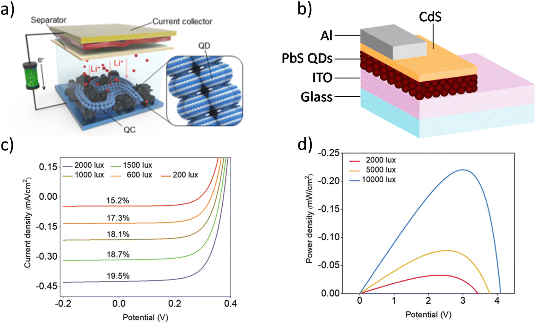 | ||
| Fig. 12 (a) Schematic structure of a CQD quantum chain incorporated into lithium-ion battery.138 (b) Structure of a typical CQD solar cell.139 (c) J–V Curves at different indoor irradiances and their respective PCE values and (d) power density–V curves at different irradiances for a PbS-based photovoltaic cell.140 | ||
Photovoltaic cells (PVCs) are devices that convert photon energy into electrical energy. This is possible if the incoming light has energy that is greater than the bandgap energy of the incident semiconductor material. The photon excites an electron across the bandgap of the material, producing an electron–hole pair. In the photovoltaic effect, unlike the photoelectric effect where the electron is emitted out of the material, the electron is confined in the material and so can be influenced by electric fields and collected. After the discovery of the photovoltaic effect by Becquerel, many people came up with different ways of converting solar energy into electrical energy. Reagan,141 Severy142 and Weston143 all patented forms of “solar cells”, but all used the heat from the Sun instead of making use of the photovoltaic effect. In 1946, Ohl was granted a patent for making the first semiconductor p–n junction cell, which he called a “light-sensitive electric device”.144 The first photovoltaic device to talk about solar energy conversion was in a Patent applied for in 1954 by Chapin, Fuller and Pearson in Bell Laboratories, called “Solar energy conversion apparatus”.145 Si was used as an n-type body and Boron was used with Si to produce a p-type body. Similar to other technologies, Si was the prominent material due to its abundance and mature technology, and is still the material used for commercial solar cells/panels. However, for high-performance and efficiency applications, Si cannot perform due to having an indirect bandgap. A typical PVC structure can be seen in Fig. 12(b), where the CdS is used as an ETL, the PbS QDs as the active layer and the ITO and Al as the electrodes.
One of the advantages of using QDs as an active layer in solar cells is Multiple Exciton Generation (MEG). MEG is a phenomenon where a photon with energy greater than the bandgap of the incident material can create more than one electron–hole pair. In bulk materials, this is called Impact Ionization (II) and it does not become effective unless the incident energy is many multiples of the bandgap. This is due to the rates of electron–phonon scattering being high, which generally converts the excess energy into heat. For example, in Si, II does not become significant until the incident photon energy reaches 3.5 eV which makes up less than 1% of the solar spectrum.146 On the other hand, in QDs, it is possible to create 2 electron–hole pairs from a photon with energy twice the size of the bandgap.
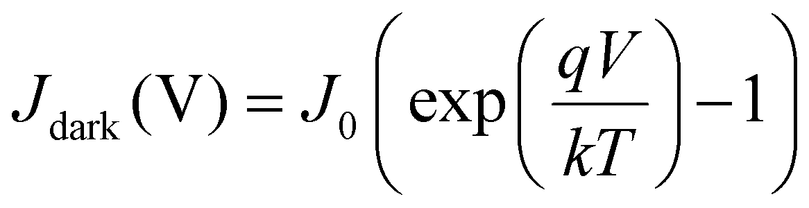
For solar cells, it is common to report current densities instead of currents directly. This is to take the area of the cells into account and make a more direct comparison of the performance of the cells. A lot of important parameters can be extracted from the current–voltage relationships of the solar cell, which starts with the assumption of an ideal diode. The ideal diode equation is given by147
 | (17) |
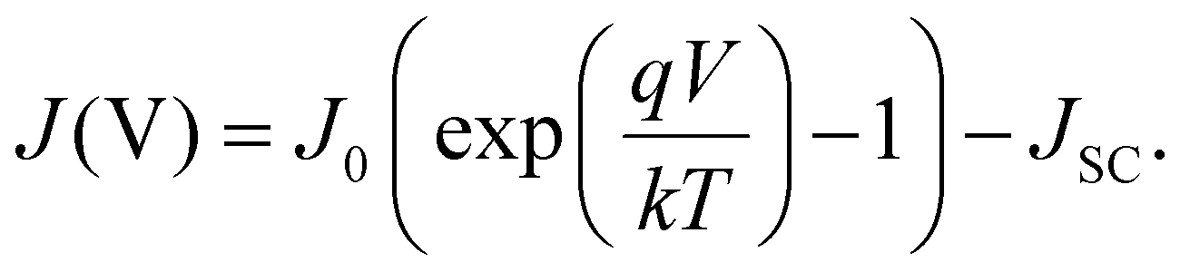 | (18) |
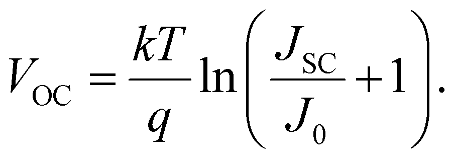
A typical J–V curve of a solar cell can be seen in Fig. 13. As seen on the graph, JSC can also be defined as the current density through the device when there is no potential difference, i.e. when the device is short-circuited. Another important parameter for solar cells is the open circuit voltage VOC, which is defined as when the potential difference has its maximum value. In other words, it is when the dark current is equal to the illumination current, so no current flows through the device. It is given by
 | (19) |
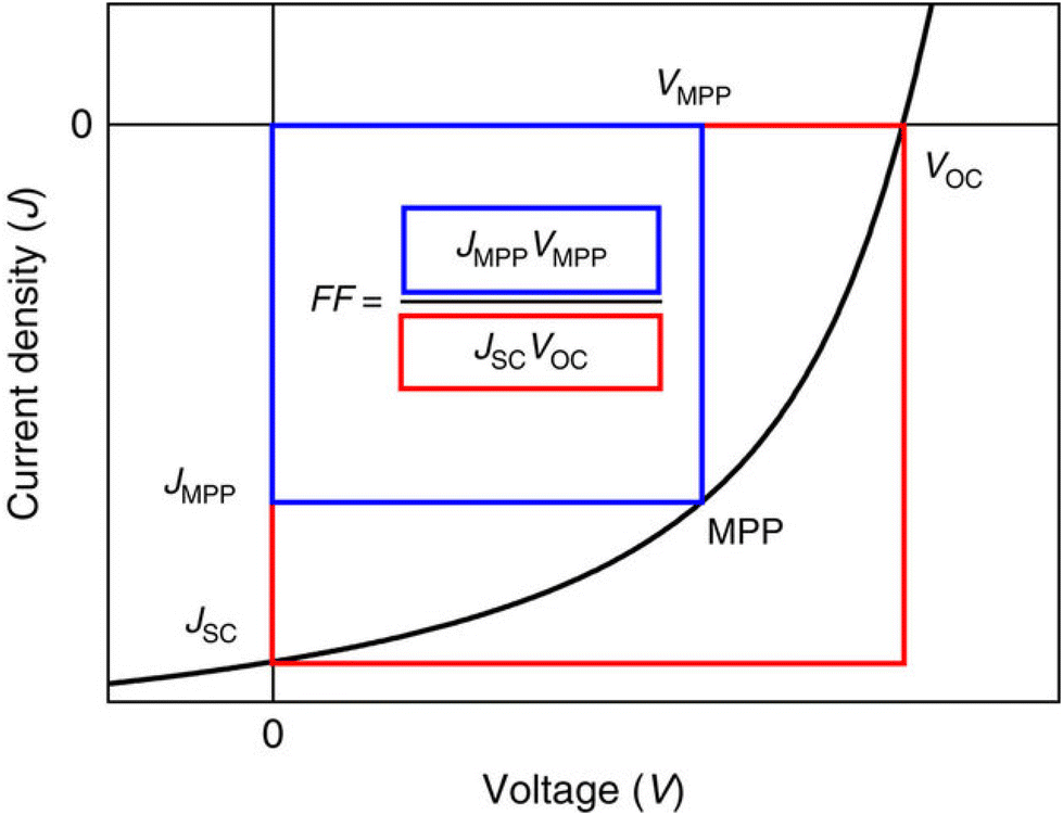 | ||
| Fig. 13 Current density–voltage graph for a photovoltaic cell, showing the positions of important parameters.148 | ||
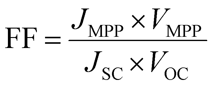
The maximum power point (MPP) of a solar cell is the maximum power output one can obtain from a cell, and the current density and voltage that this happens at are denoted as JMPP and VMPP, respectively. Finally, the Fill Factor (FF) gives the ‘squareness’ of the J–V curve. It is the ratio of the maximum actual power attainable from a solar cell to the maximum theoretical power (obtained using the maximum current density JSC and the maximum voltage VOC), and is given by
 | (20) |
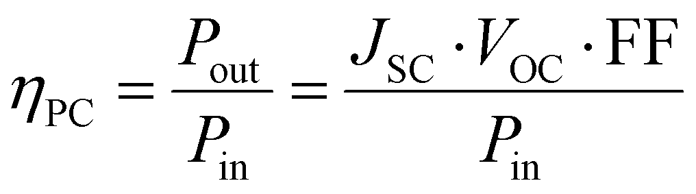
Power conversion efficiency. Power conversion efficiency (PCE), as the name suggests, is a measure of how much electrical power is obtained in comparison with the power of the incident light. It is a ratio, expressed in percentages, and is given by
 | (21) |
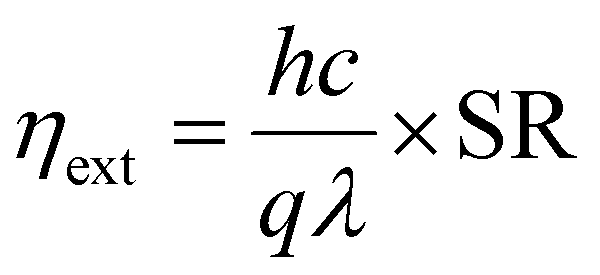
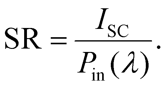
External quantum efficiency. Similar to that of a phototransistor, the EQE of a solar cell is defined as the ratio of the number of electrons collected from the device (as a result of incoming light) to the number of photons incident on the active area of the device. It is given by the equation149
 | (22) |
 | (23) |
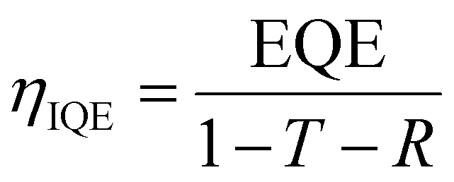
Unlike in QLEDs, the IQE in solar cells can be measured. The amount of light that is absorbed by the cell can be measured and calculated for a solar cell, whereas there is no way of knowing how much light is produced inside the QLED, only how much makes its way out. The way to calculate the true absorption (A) of a solar cell is to measure the transmission and the reflection of the incident light off the solar cell. Then, the IQE is just
 | (24) |
State-of-the-art. As the world aims to move towards decreasing the carbon footprint and emission of greenhouse gases, the transition from fossil fuels to renewable energy sources is becoming more urgent. The problem is not only limited to the source but also the use and waste of useful energy produced from these sources. Indoor photovoltaics have attracted a lot of interest, especially for IoT uses, due to their potential for converting the energy from indoor lighting into electricity for powering low-power-consumption devices. Not only does this allow for converting some of the light that is wasted for lighting a room, but it also means self-powering devices can be made which will need minimal human maintenance (e.g. no battery replacements). There are reported works where significant power efficiencies are reached when CQDs-based PVCs are exposed to both indoor irradiances and outdoor irradiances. Fig. 12(c) shows the J–V graph at different irradiance levels with their corresponding PCEs, and Fig. 12(d) shows a power density–V graph at different indoor-outdoor irradiances for a PbS CQDs-based PVC. A more detailed review of indoor photovoltaics can be found in our previous works.150,151
5. Integration
Even though CQDs have been proved to be effective in separate devices, there are still problems to overcome in order to integrate them into commercial devices for future uses. Integrated circuits (ICs) were one of the main drivers of the technological revolution, since they allowed the integration of many smaller components and transistors on the same substrate, which decreased the cost and increased the power efficiency. The first IC was made using Germanium in 1958, but Silicon ICs followed shortly in 1961. Si is the second most abundant element in the Earth's crust after oxygen, which means it is quite cheap. It can be processed and purified relatively easily, and having a natural oxide that acts as an insulator means it can be processed for both semiconductor and insulator uses. Fabricating ICs requires conventional processes that include deposition, photolithography, etching, doping and many more. These processes allow the manufacturing of ICs on wafers with sizes ranging from 1–12 inches. Some of these processes require high vacuum and temperatures and generally have high power consumption along with a high carbon footprint. As Si processing and technology matured over the years, the uses of Si spread from electronics to optoelectronics as well. Silicon-based receivers have been developed with high resolution and on-chip processing functionalities mostly due to their complementary metal–oxide–semiconductor (CMOS) compatibility, which allowed for large-scale, cheap and high-uniformity fabrication. However, two key limitations of Si have resulted in the optoelectronic properties being inferior in comparison with other semiconductor materials. The first one is the bandgap of Si, which is 1.1 eV, meaning it can only be effective in the visible to near-infrared (NIR) region. The second one is the bandgap being indirect, meaning an electron–photon interaction can only take place with an intermediate interaction with a phonon, leading to low absorption and efficiencies. II–VI, III–V and their alloys have been used in the making of optoelectronic devices for infrared applications due to their direct bandgap and energies. However, the lattice constants of such materials do not match with Si, resulting in strains and defects, which in turn lead to decreased performance. Decreasing the strains and defects means lattice matching with Si, which can be done with the use of strain-matching layers. The number of strain-matching layers needed will depend on the lattice mismatch between the required material and Si, and complicates the processing and adds to the cost.The optoelectronic properties of CQDs make them suitable for use instead of or complementary to Si. The nature of CQD solutions also means that there is no concern for lattice mismatch. In addition, the solution processability of CQDs allows the replacement of some of the previously mentioned processes with solution processing methods, potentially simplifying the fabrication process. However, solution processing techniques have drawbacks in comparison with conventional techniques, which make it hard to integrate with Si. Two examples of popularly used solution processing techniques in the literature are spin coating and inkjet printing. Spin coating, for example, can have uniformity issues when applied on large areas due to the rotation speed difference in the centre compared with the edge. It also has no selectivity, meaning it will coat the whole substrate. Etching processes are required to pattern the CQD films. In addition, spin coating only deposits around 10% or less of the solution that is dropped, meaning a lot of material is wasted, making it less feasible for commercial uses. On the other hand, inkjet printing is a selective method which can print patterns and structures accurately, and all the solution that is dropped is actually used, so there is less waste when compared with spin coating. One of the main problems with inkjet printing is the ink preparation. Variables like surface tension and viscosity of the solution are very important for the printability of the ink, which can be complicated depending on the solution that needs printing. In addition, feature size is also a big limitation for inkjet printers. Minimum feature size can range between tens to hundreds of micrometers, whereas some Si ICs use technologies that can produce feature sizes in the order of nanometers. This is particularly important for devices where minimum feature size is important. As can be seen in eqn (6), the drain current is proportional to W/L in FETs, so the performance can be improved by using smaller channel lengths, which becomes a limitation. This section will cover the possibilities and methods for integrating CQDs with conventional technologies for use in IoT applications.
The first ICs fabricated using CQDs were reported by Kim et al. in 2012.152 In this work, they used CdSe CQDs treated with thiocyanate ligand to demonstrate low-voltage inverters, amplifiers and ring oscillators. It is also mentioned that continued advances can help solution-processable nanomaterials to extend beyond unipolar circuits. CMOS makes use of complementary n-type and p-type transistors to make logic gates, which are used in ICs. They are essential in processing units and memory, which are used in almost every electronic device. It has been shown previously that treating CQD films can change their stoichiometry and electronic properties. Oh et al. in 2014 have shown that treating PbSe QDs with Na2Se can form p-type conducting films, whereas treating with PbCl2 afterwards can increase the electron concentration and form an n-type film.153 Choi et al. in 2012 used In-doped Au contacts on top of CdSe QD films which allowed for the facile thermal diffusion of In into the QD film.80 The In-doped QD film showed a 100–1000 times increase in mobility. Yun et al. in 2020 implemented similar techniques from both of these works to heavy metal-free CQDs for their use in CMOS circuits.88 They used NH4I to treat CuInSe2 CQDs and increase the p-type characteristics. The same treated CQDs were made into two different transistors with Au and In source and drain contacts. The schematic structure of these transistors can be seen in Fig. 14(a). The In from the contacts thermally diffused into the CQD layer to dope and convert it to n-type. This allowed the fabrication of CMOS circuit elements including an inverter, NAND gate and a NOR gate, by using the same type of CQDs with different material contacts. The structure and the outputs of the NAND gate can be seen in Fig. 14(b) and (c), respectively. Other active devices that are CMOS-compatible have been demonstrated in the literature as well. Zhang et al. successfully fabricated wafer-scale trapping-mode infrared imagers using HgTe CQDs on Readout ICs (ROICs).154 The trapping-mode imagers work by trapping minority carriers by a vertical built-in potential (arising from the junction between intrinsic and doped CQDs), which decreases dark current and improves efficiency. The fabrication of ROIC requires two consecutive spin coating processes, one for intrinsic and the other for doped CQDs. The resulting imagers showed a photoresponse non-uniformity of 4%, dead pixel rate of 0%, and detectivity reaching 2 × 10¹¹ at 300 K for wavelengths <2.5 μm and 8 × 10¹⁰ at 80 K for wavelengths <5.5 μm. Xu et al. demonstrated a new architecture for a detector, named photodiode–oxide–semiconductor FET (PHOSFET), that is compatible with silicon transistors.155 The proposed structure uses a photodiode with n-type and p-type PbS CQDs, topped with a 20 nm layer of Al as the top gate, which is separated from the Si channel with a 10 nm-thick oxide layer. Simulations were run that show the formation of a channel in the Si–oxide interface as the photodiode was illuminated by light. Further tests were made by connecting the photodiode to a commercially available MOSFET, which showed a PR of 5.9 A W−1 at 1250 nm.
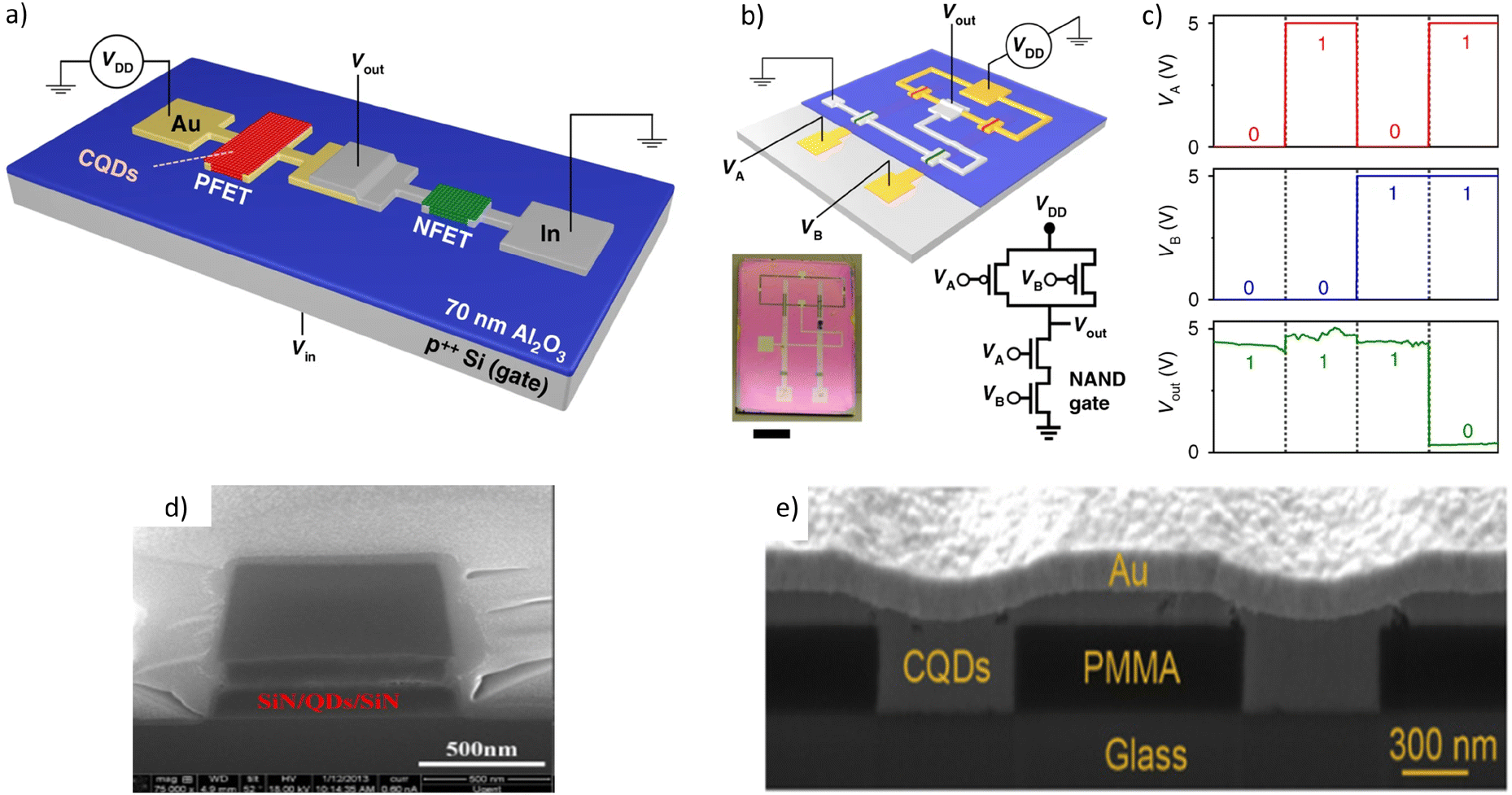 | ||
| Fig. 14 (a) The schematic structure of a CQD CMOS inverter, (b) a schematic illustration (top), its picture (bottom left) and the circuit diagram (bottom right) of a NAND gate made from the p and n-type CQD FETs and (c) the outcomes of the NAND gate for four different input configurations.88 (d) Cross-sectional SEM image of the H-SiN/CQDs/L-SiN waveguide.156 (e) Cross-sectional SEM image of a Y-splitter made from CQDs and PMMA.158 | ||
Photonics ICs (PICs) are another form of ICs that use photons instead of electrons in circuits for processing. They can increase bandwidth and transfer speeds, and decrease power consumption in comparison with electronic ICs. In ICs, the main component is the transistor. However, in PICs, there is no “main” component. Active components like lasers and detectors are used to emit and absorb light, and passive components like waveguides, power splitters and amplifiers are used to transfer, modify, redirect, etc. energy in between components. Silicon is a well-established material for passive components of PICs, but due to having an indirect bandgap, it cannot compete with direct bandgap materials when it comes to active components in PICs. For that reason, other materials like GaAs and InP are used. However, as mentioned above, using these materials complicates the manufacturing processes and increases costs. Due to the optical properties of CQDs, they are good candidates for use in PICs. For complete integration, it may be essential to use them in passive components as well. Xie et al. have demonstrated waveguides by using CdSe/CdS CQDs with an emission peak of 625 nm along with SiN.156 A cross-sectional SEM image of this waveguide can be seen in Fig. 14(d). A loss of 0.94 dB cm−1 and 1.88 dB cm−1 at 900 nm has been achieved at SiN deposition temperatures of 270 °C and 120 °C, respectively. Rong et al. in 2019 demonstrated 10 CQD-based PIC components (including laser, bending waveguide, Y-splitter, MZ interferometer and low-noise amplifier) using CdSe/ZnS CQDs with PMMA.157 Liu et al. in 2020 demonstrated a similar work by using PMMA and CdSe/ZnSe/ZnS CQDs with an emission peak of 645 nm.158 A loss of 36.2 dB cm−1 was obtained with 800 nm in straight waveguides, and other components including lasers, Y-splitters, bending waveguides, MZ interferometers were fabricated successfully. The cross-sectional SEM image of the Y-splitter can be seen in Fig. 14(e). Unlike CMOS, the use of the same CQDs for different components in PICs is a bit more complicated. The low-loss waveguides by Xie et al. were tested at a wavelength significantly longer than the emission peak of the used CQDs, meaning there would be minimal absorption losses to CQDs. However, using the same CQDs for active and passive components would not yield similar low-loss properties, due to absorption by the CQDs in the waveguides. Rong et al. compensate these losses with a low-noise optical amplifier. However, this would mean more component integration, which would complicate fabrication processes. One particular work published by Wang et al. in 2017 shows a method for direct optical lithography of inorganic nanocrystals, which include metals, oxides and semiconductors.159 This eliminates the need for photoresist usage for patterning CQD-based devices and circuits, and also is a solution to the non-selectivity of spin coating processes, which can help integrate different types of devices to circuits and help construct ICs from CQDs in a simpler way.
CQDs have also been considered for use in lasers. The main factors that led to the research on QD lasers result from the fact that the atomic-like energy levels have a wide separation. This inhibits thermal depopulation of band-edge states and reduces the optical gain threshold, since the separation between the states is >kBT. In addition, it decreases the temperature sensitivity, leading to more stable lasing.160 The main challenges for CQD lasing come with the Auger recombination rates. In bulk semiconductors, only particles above a certain kinetic energy threshold can take part in Auger recombination due to momentum conservation.161 However, in nanocrystals, this momentum conservation is relaxed due to the atomic levels classified according to angular momentum, but not translational.162 This leads to increased Auger recombination rates, which directly compete with stimulated emission. The use of dense QD films with ultrafast pumping was what led to the first demonstration of amplified spontaneous emission with CQDs in 2000.163 Since then, many optically pumped CQD lasers (OPCQDL) have been reported. Dang et al. in 2012 reported RGB lasers operating by single-exciton gain in type 1 CSQD films and the first optically pumped CQD Vertical-Cavity Surface-Emitting Laser (VCSEL), using CdSe/ZnCdS CQDs.164 The ASE thresholds for the RGB lasers were 90, 145 and 800 μJ cm−1, respectively, and the pumping threshold for the red VCSEL was around 60 μJ cm−1. Foucher et al. in 2014 reported a flexible laser with an average fluence of 450 μJ cm−1 at an emitting wavelength of 607 nm using an acrylate grating structure as a distributed feedback (DFB) laser.165 The gain medium was CdSe/ZnS CQDS in PMMA, and the emission wavelength could be tuned over a 18 nm range by the bending radius. le Feber et al. in 2018 used CdSe/CdS/ZnS CQDs to fabricate ring lasers with active colour control.166 At 25 μJ cm−1, the CdSe core starts to lase. Increasing to above 100 μJ cm−1 results in green lasing from the shell, making an orange-like emission colour. Above 250 μJ cm−1, the red lasing disappears and a pure green emission can be observed. The main issue with most of the published works is poor thermal stability. However, this could be addressed by fabricating the lasers on high thermal conductivity substrates, which is done for commercial lasers. Also, other methods like embedding CQD-assembled microspheres into silica matrix increases the heat resistance, allowing operations up to 450 K as shown by Chang et al.167
To realise the full potential and applications of CQD lasers, electrically pumped CQD lasers (EPCQDLs) are essential. CQD-based EL devices have advanced greatly in the form of QLEDs, as discussed previously in this article. The device structure of QLEDs allows the efficient injection of carriers, essentially forming a p–i–n structure. So far, the proposed structures for EPCQDLs use a similar structure to that of a QLED but additionally contain either an internal or external optical cavity for feedback into the gain medium. The main issue with using this structure is that the operating current densities of QLEDs are too low to realise lasing. Other issues are the optical losses in the charge transfer layers of the QLEDs and charge injection limitations that might be caused by integrated optical cavities. Even though EPCQDLs still haven't been fabricated successfully, the increased understanding of the nature of EL devices and facilitating efficient charge carrier injection has enabled OPCQDL and dual-function LED devices.170 Roh et al. in 2020 reported an OPCQDL with a QLED structure, that used a grated ITO for an integrated optical cavity.169 The different types of structures for optically and electrically pumped CQD lasers can be seen in Fig. 15. Collective improvements from these different subjects of research are now paving a promising path to obtaining EPCQDLs.
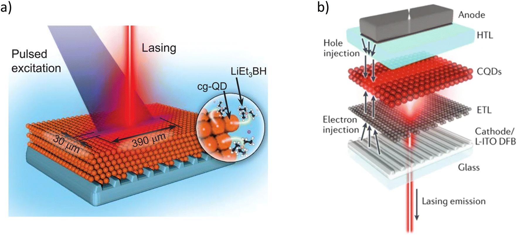 | ||
| Fig. 15 Structure of (a) an optically pumped CQD laser operating via a DFB structure168 and (b) a potential electrically pumped CQD laser, demonstrated to work by pumping optically.169 | ||
Dual-function devices also add to the potential integration of CQDs. Dual-function devices are devices that can have different functions depending on the applied bias across them. Ren et al. in 2019 implemented a heterojunction using halide perovskite and CdSe/ZnS CQDs to make a device that can operate as a multicolour LED, solar cell and a photodetector.171 The device operates as an LED in forward bias, and the recombination zone changes as the applied voltage changes. At low voltages, a red emission can be seen from the CQD layer. A green emission from the perovskite layer shows up as the voltage is increased, and matches the red peak around 3 V. Further increase of the voltage increases the green peak to red peak ratio. The addition of a PCBM layer in between the CdSe and ETL promotes electron injection, resulting in a FF of 0.72 and a PCE of 4.2% for solar cell applications. In addition, a PR of 6–10 mA W−1 is observed for light detection below 525 nm. Kim et al. in 2021 demonstrated a CQD light-emitting diode that can also operate as a photodetector (PD).172 A V2O5 layer was proposed as a HIL, and TFB and ZnO were used as HTL and ETL layers, respectively. The emissive layer was made up of CdSe/ZnS CQDs, and the whole device was fabricated using spin coating. In forward bias, the device operates as a QLED, with a turn-on voltage around 2.6 V and emission at 536 nm. In reverse bias, the device operates as a PD, with a photoresponsivity of 0.0076 A W−1. An output signal was demonstrated from the PD connected to an operational amplifier that resulted from an input signal from the QLED. A similar study was done by Ju et al. in 2022 using perovskite QDs (PQDs).173 PEDOT:PSS, PTAA, TPBi and LiF were used as HIL, HTL, ETL and EIL, respectively. The device operates as a QLED in forward bias, with a turn-on voltage of 2.4 V and an EL peak at 519 nm. The introduction of copper thiocyanate (CuSCN) in between the PEDOT:PSS and PTAA layer increases the max CE and average EQE of the device by 150% and 136%, respectively. The device also shows a response to light with wavelengths <450 nm, which is due to the presence of the photosensitive PTAA layer. PD tests show that the device signal does not return to the original levels after light illumination is stopped, showing the potential of “remembering” previous states, which can later be erased by applying a reverse bias. Dual-functional device structures are not only limited to the vertical LED structure. Compared with the devices mentioned in this article, the light-emitting transistor (LET) is a less mature technology which has been discovered recently. It brings together the light-emitting properties of a diode and the switching properties of a transistor. Using a similar structure to the FEPTs discussed in the previous section, Bera et al. in 2019 successfully fabricated a vertical phototransistor that can both emit and detect light with a suitable bias.174 This was achieved by sandwiching a PQD layer between two graphene layers, on top of a highly doped Si/SiO2 substrate. The source and drain contact material was chosen to be Au. The resulting phototransistor had an EQE over 1010%, PR of >109 A W−1 and a response time of 50 μs. The LET showed an EQE of 5.6%, with an emission at 530 nm. The possibility of fabricating dual-function devices with the same structure opens a range of applications for the integration of CQDs, meaning device arrays can be created on the same substrate that will have identical structures and different functionalities.
Dual-function devices can be taken a step further. There are reported works of dual-function devices that can operate in both light-emitting and sensing modes simultaneously, which can lead to new applications. Oh et al. in 2017 have used double heterojunction nanorods (DHNR) to make a vertically stacked LED that can operate both as an emitter and a PD.175 The structure of this device can be seen in Fig. 16(a). The LED exhibits an EQE of 8% at 1000 m2, a low turn-on voltage of 1.7 V and a maximum brightness >80000 m2. The PD shows a photocurrent to dark current ratio of 3 × 10⁴, and a responsivity of 22 mA W−1 and 200 mA W−1 at 532 nm and 400 nm, respectively. The J–V graph of the PD can be seen in Fig. 16(b). Due to the fast response of the devices, it is possible to alternate between forward and reverse bias in submillisecond timescales. This allows for the operation of the PD in between forward bias operations, while the submillisecond timescale allows for the light emission to appear continuous to the human eye. Identical devices can also communicate with each other, and this is demonstrated at both 10 and 50 kHz and can be seen in Fig. 16(d). By using the photocurrent, it is possible to automatically control the brightness of the device. A demonstration of this can be seen in Fig. 16(c), where the incoming LED or finger affects the brightness of the device. Shi et al. in 2020 demonstrated a similar simultaneous operation vertical LED that used a multiple quantum well (MQW) as the active layer.176 The device was built on a III-nitride-on-silicon platform. First, a communication test was done between two identical devices, where one acts as a transmitter and the other as a receiver, and communication of up to 2 Mbps was observed. The simultaneous emission and detection was also tested using a 405 nm laser pointer. The measured current from the device is the sum of the driving current and the photocurrent, meaning the photocurrent can be extracted. The photocurrent can be fed back to the driving current which can autonomously adjust the brightness of the emitted light. Fu et al. used a similar MQW diode structure to demonstrate simultaneous emitting and detecting properties.177 A 4 × 4 array of these devices was demonstrated to work as a potential smart screen that can be used as a display and camera at the same time. The MQW diode also showed promising results regarding refresh rates which meet the requirements of most screen resolutions, and has also shown that it can detect a 1 Mbps signal. Demonstrating simultaneous dual-function devices using DHNR and MQWs also opens up opportunities for new applications including interactive and touchless displays. Even though not demonstrated yet, CQDs are also candidates for use in these devices. Nonetheless, the main difficulty arises from the structure of CQDs. The type 1 core–shell structure CQD enhances the PL and EL due to the better confinement of charge carriers, but results in a barrier for carrier extraction. Removing the shell would aid carrier extraction properties but would significantly decrease the EL and PL performance.
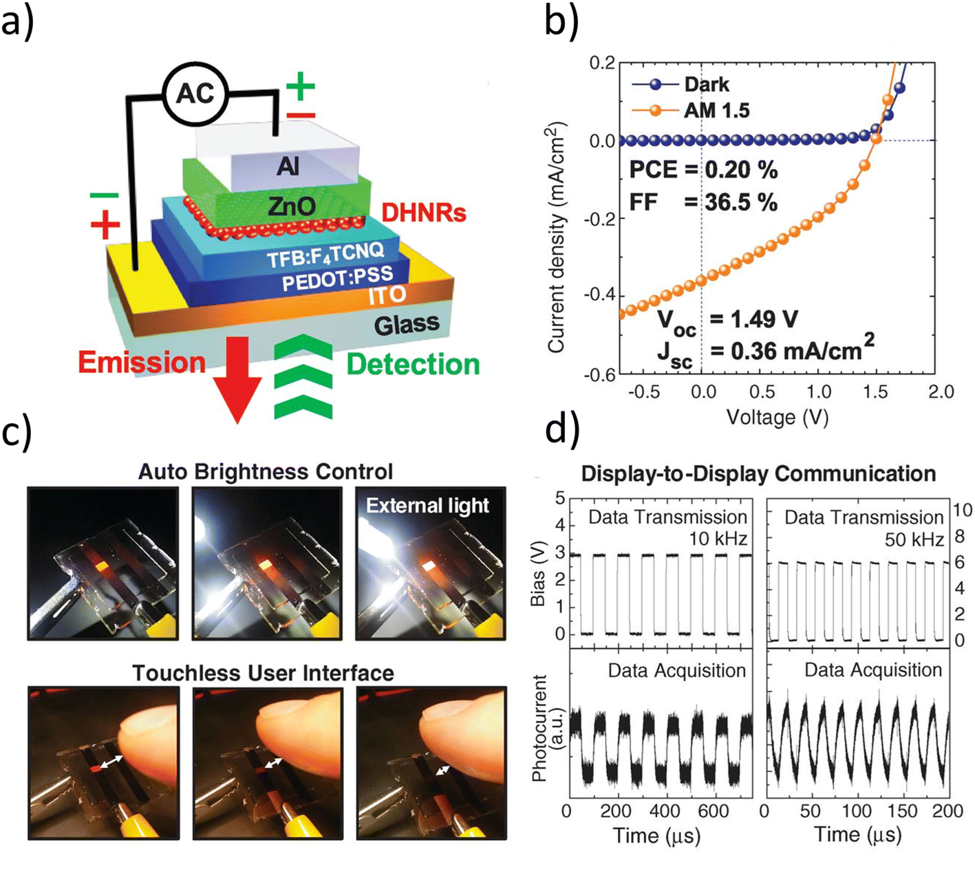 | ||
| Fig. 16 (a) Structure of the dual-function DHNR device. (b) The J–V characteristics of the device under Dark and AM 1.5 (100 mW cm−2 conditions. c) The automatic brightness control in response to an LED and finger approaching the device. (d) Data transmission and acquisition between two identical devices at 10 and 50 kHz.175 | ||
Visible Light Communication (VLC) and LiFi are two technologies that can benefit greatly from CQDs. VLC is the use of visible light (780–375 nm) to transmit signals and data, whereas LiFi is an extension of VLC to ultraviolet and infrared regions. Historically, <10 GHz band has been used for wireless communication purposes, but due to the increase in the demand for wireless communication, it is becoming insufficient. Communications >10 GHz have been proposed to overcome this issue, and LiFi is a derivative of this band. The term LiFi was first introduced by Herald Haas in his TEDGlobal talk in 2011, and it is classified as nm-wave communication. It uses μLEDs for communication that can reach rates higher than Gb s−1. Wang et al. in 2021 used a nanostructured InGaN wetting layer as an active region for a blue μLED and achieved a 4 Gbps VLC system.178 Wei et al. in 2022 reported a 2.1 Gbps online and 5 Gbps offline system using InGaN QDs as the active region.179 These μLEDs were fabricated using conventional metal–organic vapor phase epitaxy (MOVPE). CQDs have also been tested for use in VLC and LiFi systems. Tankimanova et al. in 2021 used PbS CQDs as colour converters absorbing in the visible range and emitting in the eye-safe NIR range, achieving transmission rates of 0.27 Mbps, enough to support an indoor optical IoT system.180 Leitao et al. used CdSSe/ZnS CQDs as colour converters for InGaN sources, achieving transmission rates up to 1 Gbps over >10 cm distances.181 LiFi has several advantages worth mentioning. Using visible light for communication means decreasing the “wasted” light used solely for lighting. The nature of visible light also means that LiFi can only be used in the installed rooms, making it less accessible from the outside and therefore safer. Since no antenna is used, it is also safer to use in flammable environments due to there being no risks for spark formation.182
Fig. 17 shows the different areas CQDs could be implemented in future IoT applications. Areas like display, detectors, photovoltaics and lighting have already been matured and have comparable performances to the state-of-the-art, whereas other areas have promising demonstrations but are not quite mature enough. The main difficulty with integrating CQDs comes with the compatibility of their processing techniques with the conventional techniques already used for commercial applications. In addition, as the infrastructure is being built continuously on existing technologies, there is not much room for setbacks in terms of performance, in exchange for costs and lower carbon footprints. However, it is more probable for CQDs to be implemented in new types of applications, where flexibility and transparency are required. So even though replacing current technologies in some areas with CQDs seems far away, the published research shows very promising results for their use in new applications. Covering so many different areas, CQDs are paving the way to make themselves good candidates in IoT devices.
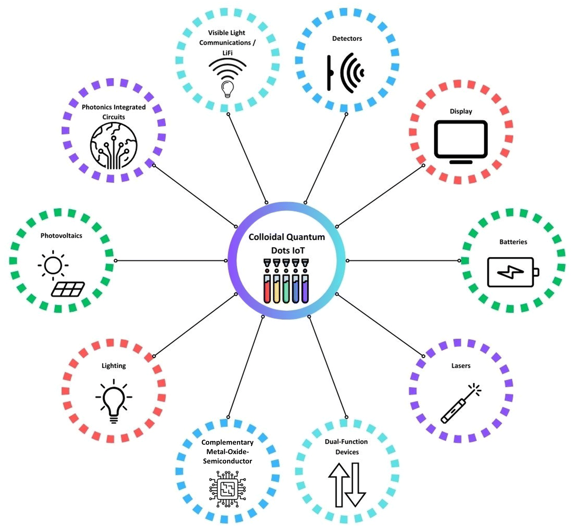 | ||
| Fig. 17 The different ways CQDs can be implemented for future IoT applications. | ||
6. Discussion and conclusions
To conclude, even though CQDs have shown great potential in making isolated high-performance optoelectronic devices, cost-effective, large-scale and commercially viable methods are needed to integrate them into IoT devices. One possibility is the integration of CQD devices with other components on separate layers, similar to that of AMOLED displays. This would allow the fabrication of CQD devices separately using already popular methods like spin coating, and connecting them using methods like wire bonding, which might not be very feasible for large-scale production. The ideal method of integrating CQD devices would be to fabricate them on the same chip. Printing methods like inkjet printing seem to be very suitable for this type of integration due to the selective area processing. However, with the current technology, the minimum feature size is an important limitation, meaning that inkjet printing would only be useful for printing on low-density chips. The demonstration of the use of CQDs for passive components and CMOS circuits also opens up possibilities of fully CQD-based chips, where the same type of CQD can be used in circuits and optoelectronic devices. However, this would require careful design and patterning techniques like etching. Nonetheless, the research on the use of CQDs for passive components and circuits is still quite immature, and more research in the upcoming years will help make up a more complete picture of the future possibilities awaiting CQDs.Conflicts of interest
There are no conflicts to declare.Acknowledgements
The authors acknowledge the financial support from the EPSRC SWIMS (EP/V039717/1), the Royal Society (RGS/R1/221009 and IEC/NSFC/211201), the Leverhulme Trust (RPG-2022-263) and Sêr Cymru programme – Enhancing Competitiveness Equipment Awards 2022–23 (MA/VG/2715/22-PN66). DMO and BH also acknowledge EPSRC CDT in Compound Semiconductor Manufacturing (EP/S024441/1) and Huawei Cambridge for funding the studentship. NH acknowledges the support of the UK government Department for Science, Innovation and Technology through the UK National Quantum Technologies Programme.References
- K. Rose, S. D. Eldridge and L. Chapin, The Internet Of Things: An Overview Understanding the Issues and Challenges of a More Connected World, 2015 Search PubMed.
- L. Manna, The Bright and Enlightening Science of Quantum Dots, Nano Lett., 2023, 23, 9673–9676 CrossRef CAS PubMed.
- B. Hou, F. C. Mocanu and Y. Cho, et al., Evolution of Local Structural Motifs in Colloidal Quantum Dot Semiconductor Nanocrystals Leading to Nanofaceting, Nano Lett., 2023, 23, 2277–2286 CrossRef CAS PubMed.
- E. Borovitskaya and M. S. Shur, Quantum Dots, World Scientific Publishing Company, Singapore, Singapore, 2002 Search PubMed.
- J. S. Blakemore, Solid State Physics, University Press, Cambridge, 2nd edn, 1985 Search PubMed.
- M. Rudan, Physics of Semiconductor Devices, Springer International Publishing, Cham, 2nd edn, 2018 Search PubMed.
- B. J. V. Zeghbroeck, Principles of Semiconductor Devices, Bart Van Zeghbroeck, 2011 Search PubMed.
- D. J. Griffiths, Introduction to Quantum Mechanics, Prentice Hall, Inc., United States Of America, 1995 Search PubMed.
- H.-J. Byun, J. C. Lee and H. Yang, Solvothermal synthesis of InP quantum dots and their enhanced luminescent efficiency by post-synthetic treatments, J. Colloid Interface Sci., 2011, 355, 35–41 CrossRef CAS PubMed.
- W. Ahmad, J. He and Z. Liu, et al., Lead Selenide (PbSe) Colloidal Quantum Dot Solar Cells with >10% Efficiency, Adv. Mater., 2019, 31, 1900593 CrossRef PubMed.
- R. Ulbricht, J. J. H. Pijpers and E. Groeneveld, et al., Loosening Quantum Confinement: Observation of Real Conductivity Caused by Hole Polarons in Semiconductor Nanocrystals Smaller than the Bohr Radius, Nano Lett., 2012, 12, 4937–4942 CrossRef CAS PubMed.
- U. Thupakula, A. Jena and A. H. Khan, et al., Synthesis, structure and electronic properties of ultranarrow CdS nanorods, J. Nanopart. Res., 2012, 14, 701 CrossRef.
- G. Bell, A. I. Filin and D. A. Romanov, et al., Direct growth of CdSe semiconductor quantum dots in glass matrix by femtosecond laser beam, Appl. Phys. Lett., 2016, 108, 063112 CrossRef.
- T. E. J. Campbell-Ricketts, N. A. J. M. Kleemans and R. Nötzel, et al., The role of dot height in determining exciton lifetimes in shallow InAs/GaAs quantum dots, Appl. Phys. Lett., 2010, 96, 033102 CrossRef.
- A. Wolkenberg and T. Przesławski, Charge transport diagnosis by: I-V (resistivity), screening and Debye length, mean free path, Mott effect and Bohr radius in InAs, In0.53Ga0.47As and GaAs MBE epitaxial layers, Appl. Surf. Sci., 2008, 254, 6736–6741 CrossRef CAS.
- Z. Long, W. Zhang and J. Tian, et al., Recent research on the luminous mechanism, synthetic strategies, and applications of CuInS 2 quantum dots, Inorg. Chem. Front., 2021, 8, 880–897 RSC.
- M. Baranowski and P. Plochocka, Excitons in Metal-Halide Perovskites, Adv. Energy Mater., 2020, 10, 1903659 CrossRef CAS.
- S.-T. Ha, R. Su and J. Xing, et al., Metal halide perovskite nanomaterials: synthesis and applications, Chem. Sci., 2017, 8, 2522–2536 RSC.
- J. Greensite, An Introduction to Quantum Theory, 2017 Search PubMed.
- Z. Liu, C. Chang and W. Zhang, et al., Research on Ligand Properties of CdSe Quantum Dots, IOP Conf. Ser.: Mater. Sci. Eng., 2019, 562, 012067 CrossRef CAS.
- Z. Ning, M. Molnár and Y. Chen, et al., Role of surface ligands in optical properties of colloidal CdSe/CdS quantum dots, Phys. Chem. Chem. Phys., 2011, 13, 5848–5854 RSC.
- A. Sahu and D. Kumar, Core-shell quantum dots: A review on classification, materials, application, and theoretical modeling, J. Alloys Compd., 2022, 924, 166508 CrossRef CAS.
- A. Ekimov, Quantum size effect in three-dimensional microscopic semiconductor crystals, JETP Lett., 1981, 34, 345 Search PubMed.
- A. I. Ekimov and A. A. Onushchenko, Quantum size effect in the optical-spectra of semiconductor micro-crystals, Sov. Phys. Semicond., 1982, 16, 775–778 Search PubMed.
- A. I. Ekimov, A. L. Efros and A. A. Onushchenko, Quantum size effect in semiconductor microcrystals, Solid State Commun., 1985, 56, 921–924 CrossRef CAS.
- R. Rossetti, S. Nakahara and L. E. Brus, Quantum size effects in the redox potentials, resonance Raman spectra, and electronic spectra of CdS crystallites in aqueous solution, J. Chem. Phys., 1983, 79, 1086–1088 CrossRef CAS.
- M. G. Bawendi, M. L. Steigerwald and L. E. Brus, The Quantum Mechanics of Larger Semiconductor Clusters (“Quantum Dots”), Annu. Rev. Phys. Chem., 1990, 41, 477–496 CrossRef CAS.
- C. B. Murray, D. J. Norris and M. G. Bawendi, Synthesis and characterization of nearly monodisperse CdE (E = sulfur, selenium, tellurium) semiconductor nanocrystallites, J. Am. Chem. Soc., 1993, 115, 8706–8715 CrossRef CAS.
- W. A. A. Mohamed, H. A. El-Gawad and S. Mekkey, et al., Quantum dots synthetization and future prospect applications, Nanotechnol. Rev., 2021, 10, 1926–1940 CrossRef CAS.
- S.-M. Liu, H.-Q. Guo and Z.-H. Zhang, et al., Characterization of CdSe and CdSe/CdS core/shell nanoclusters synthesized in aqueous solution, Phys. E, 2000, 8, 174–178 CrossRef CAS.
- Z. A. Peng and X. Peng, Formation of High-Quality CdTe, CdSe, and CdS Nanocrystals Using CdO as Precursor, J. Am. Chem. Soc., 2001, 123, 183–184 CrossRef CAS PubMed.
- R. K. Čapek, K. Lambert and D. Dorfs, et al., Synthesis of Extremely Small CdSe and Bright Blue Luminescent CdSe/ZnS Nanoparticles by a Prefocused Hot-Injection Approach, Chem. Mater., 2009, 21, 1743–1749 CrossRef.
- B. Hou, D. Benito-Alifonso and R. Webster, et al., Rapid phosphine-free synthesis of CdSe quantum dots: promoting the generation of Se precursors using a radical initiator, J. Mater. Chem. A, 2014, 2, 6879–6886 RSC.
- B. Hou, Y. Cho and B.-S. Kim, et al., Red green blue emissive lead sulfide quantum dots: heterogeneous synthesis and applications, J. Mater. Chem. C, 2017, 5, 3692–3698 RSC.
- S. Chan, M. Liu and K. Latham, et al., Monodisperse and size-tunable PbS colloidal quantum dots via heterogeneous precursors, J. Mater. Chem. C, 2017, 5, 2182–2187 RSC.
- D. Deng, W. Zhang and X. Chen, et al., Facile Synthesis of High-Quality, Water-Soluble, Near-Infrared-Emitting PbS Quantum Dots, Eur. J. Inorg. Chem., 2009, 2009, 3440–3446 CrossRef.
- M. Hines and G. Scholes, Colloidal PbS Nanocrystals with Size-Tunable Near-Infrared Emission: Observation of Post-Synthesis Self-Narrowing of the Particle Size Distribution, Adv. Mater., 2003, 15, 1844–1849 CrossRef CAS.
- B. Hou, Y. Cho and B. S. Kim, et al., Highly Monodispersed PbS Quantum Dots for Outstanding Cascaded-Junction Solar Cells, ACS Energy Lett., 2016, 1, 834–839 CrossRef CAS PubMed.
- Y. Kim, S. Ham and H. Jang, et al., Bright and Uniform Green Light Emitting InP/ZnSe/ZnS Quantum Dots for Wide Color Gamut Displays, ACS Appl. Nano Mater., 2019, 2, 1496–1504 CrossRef CAS.
- Y.-H. Won, O. Cho and T. Kim, et al., Highly efficient and stable InP/ZnSe/ZnS quantum dot light-emitting diodes, Nature, 2019, 575, 634–638 CrossRef CAS PubMed.
- T. Yuan, F. Yuan and L. Sui, et al., Carbon Quantum Dots with Near-Unity Quantum Yield Bandgap Emission for Electroluminescent Light-Emitting Diodes, Angew. Chem., 2023, 135, e202218568 CrossRef.
- S. Ghosh, S. Mandal and S. Mukherjee, et al., Near-Unity Photoluminescence Quantum Yield and Highly Suppressed Blinking in a Toxic-Metal-Free Quantum Dot, J. Phys. Chem. Lett., 2021, 12, 1426–1431 CrossRef CAS PubMed.
- S.-W. Dai, B.-W. Hsu and C.-Y. Chen, et al., Perovskite Quantum Dots with Near Unity Solution and Neat-Film Photoluminescent Quantum Yield by Novel Spray Synthesis, Adv. Mater., 2018, 30, 1705532 CrossRef PubMed.
- S. Ren, M. Wang and X. Wang, et al., Near-infrared heavy-metal-free SnSe/ZnSe quantum dots for efficient photoelectrochemical hydrogen generation, Nanoscale, 2021, 13, 3519–3527 RSC.
- J. Zhou, J. Huang and H. Chen, et al., Low-Cost Synthesis of Silicon Quantum Dots with Near-Unity Internal Quantum Efficiency, J. Phys. Chem. Lett., 2021, 12, 8909–8916 CrossRef CAS PubMed.
- Y. You, X. Tong and A. Imran Channa, et al., High-efficiency luminescent solar concentrators based on Composition-tunable Eco-friendly Core/shell quantum dots, Chem. Eng. J., 2023, 452, 139490 CrossRef CAS.
- R. Wu, T. Wang and M. Wu, et al., Synthesis of highly stable CuInZnS/ZnS//ZnS quantum dots with thick shell and its application to quantitative immunoassay, Chem. Eng. J., 2018, 348, 447–454 CrossRef CAS.
- G. Almeida, R. F. Ubbink and M. Stam, et al., InP colloidal quantum dots for visible and near-infrared photonics, Nat. Rev. Mater., 2023, 8, 742–758 CrossRef CAS.
- W. Stallings, Foundations of Modern Networking: SDN, NFV, QoE, IoT, and Cloud, Addison-Wesley Professional, 1st edn, 2015 Search PubMed.
- M. Weiser, The Computer for the 21 st Century, Sci. Am., 1991, 265, 94–105 CrossRef.
- D. Evans, How the Next Evolution of the Internet Is Changing Everything, 2011, p. 11 Search PubMed.
- R. Hassan, F. Qamar and M. K. Hasan, et al., Internet of Things and Its Applications: A Comprehensive Survey, Symmetry, 2020, 12, 1674 CrossRef.
- L. Qian, Z. Luo and Y. Du, et al., Cloud Computing, Berlin, Heidelberg, 2009, pp. 626–631 Search PubMed.
- D. Zhang, C. C. Chan and G. Y. Zhou, Enabling Industrial Internet of Things (IIoT) towards an emerging smart energy system, Global Energy Interconnect., 2018, 1, 39–47 Search PubMed.
- M. K. Yogi, K. C. Sekhar and G. V. Kumar, Mist Computing: Principles, Trends and Future Direction, Int. J. Comput. Eng. Res., 2017, 4, 19–21 Search PubMed.
- A. M. A. Ferreira, L. J. d. M. d. Azevedo and J. C. Estrella, et al., Case Studies with the Contiki-NG Simulator to Design Strategies for Sensors’ Communication Optimization in an IoT-Fog Ecosystem, Sensors, 2023, 23, 2300 CrossRef PubMed.
- C. R. Kagan, C. B. Murray and M. Nirmal, et al., Electronic Energy Transfer in CdSe Quantum Dot Solids, Phys. Rev. Lett., 1996, 76, 1517–1520 CrossRef CAS PubMed.
- C. Wang, M. Shim and P. Guyot-Sionnest, Electrochromic Nanocrystal Quantum Dots, Science, 2001, 291, 2390–2392 CrossRef CAS PubMed.
- D. Yu, C. Wang and P. Guyot-Sionnest, n-Type Conducting CdSe Nanocrystal Solids, Science, 2003, 300, 1277–1280 CrossRef CAS PubMed.
- C. R. Kagan, A. Afzali and R. Martel, et al., Evaluations and Considerations for Self-Assembled Monolayer Field-Effect Transistors, Nano Lett., 2003, 3, 119–124 CrossRef CAS.
- M. V. Kovalenko, M. Scheele and D. V. Talapin, Colloidal Nanocrystals with Molecular Metal Chalcogenide Surface Ligands, Science, 2009, 324, 1417–1420 CrossRef CAS PubMed.
- M. Scheele, N. Oeschler and I. Veremchuk, et al., Thermoelectric Properties of Lead Chalcogenide Core-Shell Nanostructures, ACS Nano, 2011, 5, 8541–8551 CrossRef CAS PubMed.
- J. E. Lilienfeld, Method and Apparatus for Controlling Electric Currents, US1745175A, 1930.
- J. E. Lilienfeld, Device for Controlling Electric Current, US1900018A, 1933.
- J. E. Lilienfeld, Amplifier for Electric Currents, US1877140A, 1932.
- O. Heil, Improvements in or Relating to Electrical Amplifiers and Other Control Arrangements and Devices, GB439457A, 1935.
- P. K. Weimer, The TFT A New Thin-Film Transistor, Proc. IRE, 1962, 50, 1462–1469 Search PubMed.
- H. Klauk, Organic thin-film transistors, Chem. Soc. Rev., 2010, 39, 2643–2666 RSC.
- H. A. Klasens and H. Koelmans, A tin oxide field-effect transistor, Solid-State Electron., 1964, 7, 701–702 CrossRef CAS.
- G. Boesen and J. Jacobs, ZnO field-effect transistor, Proc. IEEE, 1968, 56, 2094–2095 Search PubMed.
- P. G. Le Comber, W. E. Spear and A. Ghaith, Amorphous-silicon field-effect device and possible application, Electron. Lett., 1979, 6, 179–181 CrossRef.
- P. F. Carcia, R. S. McLean and M. H. Reilly, et al., Transparent ZnO thin-film transistor fabricated by rf magnetron sputtering, Appl. Phys. Lett., 2003, 82, 1117–1119 CrossRef CAS.
- S. Masuda, K. Kitamura and Y. Okumura, et al., Transparent thin film transistors using ZnO as an active channel layer and their electrical properties, J. Appl. Phys., 2003, 93, 1624–1630 CrossRef CAS.
- R. L. Hoffman, B. J. Norris and J. F. Wager, ZnO-based transparent thin-film transistors, Appl. Phys. Lett., 2003, 82, 733–735 CrossRef CAS.
- D. V. Talapin and C. B. Murray, PbSe Nanocrystal Solids for n- and p-Channel Thin Film Field-Effect Transistors, Science, 2005, 310, 86–89 CrossRef CAS PubMed.
- S. R. Bhalerao, D. Lupo and P. R. Berger, Flexible, solution-processed, indium oxide (In2O3) thin film transistors (TFT) and circuits for internet-of-things (IoT), Mater. Sci. Semicond. Process., 2022, 139, 106354 CrossRef CAS.
- E. Fortunato, P. Barquinha and R. Martins, Oxide Semiconductor Thin-Film Transistors: A Review of Recent Advances, Adv. Mater., 2012, 24, 2945–2986 CrossRef CAS PubMed.
- E. Elahi, M. Suleman and S. Nisar, et al., Robust approach towards wearable power efficient transistors with low subthreshold swing, Mater. Today Phys., 2023, 30, 100943 CrossRef CAS.
- H. Sirringhaus, 25th Anniversary Article: Organic Field-Effect Transistors: The Path Beyond Amorphous Silicon, Adv. Mater., 2014, 26, 1319–1335 CrossRef CAS PubMed.
- J.-H. Choi, A. T. Fafarman and S. J. Oh, et al., Bandlike Transport in Strongly Coupled and Doped Quantum Dot Solids: A Route to High-Performance Thin-Film Electronics, Nano Lett., 2012, 12, 2631–2638 CrossRef CAS PubMed.
- S. Zhan, S. Han and S. Y. Bang, et al., Hybrid Passivation for Foldable Indium Gallium Zinc Oxide Thin-Film Transistors Mediated by Low-Temperature and Low-Damage Parylene-C/Atomic Layer Deposition-AlOx Coating, Phys. Status Solidi A, 2020, 217, 1900832 CrossRef CAS.
- W. Qi, Q. Xu and Z. Yiqi, et al., Highly stable, low-voltage operable high-mobility flexible organic thin-film transistors based on a tri-layer gate dielectric, Flex. Print. Electron., 2022, 7, 014012 CrossRef CAS.
- M. H. Rabbi, S. Lee and D. Sasaki, et al., Polycrystalline InGaO Thin-Film Transistors with Coplanar Structure Exhibiting Average Mobility of 78 cm2 V−1 s−1 and Excellent Stability for Replacing Current Poly-Si Thin-Film Transistors for Organic Light-Emitting Diode Displays, Small Methods, 2022, 6, 2200668 CrossRef CAS PubMed.
- B. Huang, Y. Wang and L. Li, et al., MoS2-Thin Film Transistor Based Flexible 2T1C Driving Circuits for Active-Matrix Displays, Nano Lett., 2023, 23, 9333–9339 CrossRef PubMed.
- Y. Liu, Y. Yu and T. Li, et al., High Performance and High Yield Solution Processed IGZO Thin Film Transistors Fabricated with Low-Temperature Annealed Hafnium Dioxide Gate Dielectric, Adv. Electron. Mater., 2023, 9, 2300415 CrossRef CAS.
- S. Chen, Y. Luo and J. Liang, et al., Performance Enhancement of In2O3 Thin-Film Transistors via Multi-Spin Coating Combined with UV-Assisted Thermal Annealing, J. Electron. Mater., 2022, 51, 6297–6304 CrossRef CAS.
- P. Xie, T. Liu and J. Sun, et al., Solution-processed ultra-flexible C8-BTBT organic thin-film transistors with the corrected mobility over 18 cm2/(V s), Sci. Bull., 2020, 65, 791–795 CrossRef CAS PubMed.
- H. J. Yun, J. Lim and J. Roh, et al., Solution-processable integrated CMOS circuits based on colloidal CuInSe2 quantum dots, Nat. Commun., 2020, 11, 5280 CrossRef CAS PubMed.
- M. Bansal and R. R. Maiya, Phototransistor: The Story So Far, J. Electron. Inf., 2020, 2, 202–210 Search PubMed.
- J. N. Shive, The Phototransistor, Bell Laboratories Record, 1950, vol. 28, pp. 337–342 Search PubMed.
- R. R. Bockemuehl, Cadmium Sulfide Field Effect Phototransistor, Proc. IRE, 1960, 48, 875–882 CAS.
- P. C. Y. Chow and T. Someya, Organic Photodetectors for Next-Generation Wearable Electronics, Adv. Mater., 2020, 32, 1902045 CrossRef CAS PubMed.
- S. Pak, Y. Cho and J. Hong, et al., Consecutive Junction-Induced Efficient Charge Separation Mechanisms for High-Performance MoS2/Quantum Dot Phototransistors, ACS Appl. Mater. Interfaces, 2018, 10, 38264–38271 CrossRef CAS PubMed.
- S. Zhan, X.-B. Fan and J. Zhang, et al., Lattice marginal reconstruction-enabled high ambient-tolerance perovskite quantum dot phototransistors, J. Mater. Chem. C, 2020, 8, 16001–16009 RSC.
- N. Li, Z. Lan and L. Cai, et al., Advances in solution-processable near-infrared phototransistors, J. Mater. Chem. C, 2019, 7, 3711–3729 RSC.
- H. Yoo, I. S. Lee and S. Jung, et al., A Review of Phototransistors Using Metal Oxide Semiconductors: Research Progress and Future Directions, Adv. Mater., 2021, 33, 2006091 CrossRef CAS PubMed.
- A. Bala, N. Liu and A. Sen, et al., Low-Temperature Plasma-Assisted Growth of Large-Area MoS2 for Transparent Phototransistors, Adv. Funct. Mater., 2022, 32, 2205106 CrossRef CAS.
- T. Chen, S. Zhan and B. Li, et al., A Low-Toxic Colloidal Quantum Dots Sensitized IGZO Phototransistor Array for Neuromorphic Vision Sensors, Adv. Opt. Mater., 2023, 2302451 Search PubMed.
- M. M. Hasan, E. Moyen and J. K. Saha, et al., Solution processed high performance perovskite quantum dots/ZnO phototransistors, Nano Res., 2022, 15, 3660–3666 CrossRef CAS.
- J. Kim, S. M. Kwon and C. Jo, et al., Highly Efficient Photo-Induced Charge Separation Enabled by Metal-Chalcogenide Interfaces in Quantum-Dot/Metal-Oxide Hybrid Phototransistors, ACS Appl. Mater. Interfaces, 2020, 10 Search PubMed.
- Y. Dong, M. Chen and W. K. Yiu, et al., Solution Processed Hybrid Polymer: HgTe Quantum Dot Phototransistor with High Sensitivity and Fast Infrared Response up to 2400 nm at Room Temperature, Adv. Sci., 2020, 7, 2000068 CrossRef CAS PubMed.
- E. Lhuillier, S. Keuleyan and P. Zolotavin, et al., Mid-Infrared HgTe/As2S3 Field Effect Transistors and Photodetectors, Adv. Mater., 2013, 25, 137–141 CrossRef CAS PubMed.
- C. Zhang, X. Yin and G. Qian, et al., Gate Voltage Adjusting PbS-I Quantum-Dot-Sensitized InGaZnO Hybrid Phototransistor with High-Sensitivity, Adv. Funct. Mater., 2023, 2308897 Search PubMed.
- K. Shi, J. Li and Y. Xiao, et al., High-Response, Ultrafast-Speed, and Self-Powered Photodetection Achieved in InP@ZnS-MoS2 Phototransistors with Interdigitated Pt Electrodes, ACS Appl. Mater. Interfaces, 2020, 12, 31382–31391 CrossRef CAS PubMed.
- N. Holonyak and S. F. Bevacqua, Coherent (visible) light emission from Ga(As1−xPx) junctions, Appl. Phys. Lett., 1962, 1, 82–83 CrossRef CAS.
- C. M. Bourget, An Introduction to Light-emitting Diodes, HortScience, 2008, 43, 1944–1946 Search PubMed.
- A. Bernanose and P. Vouaux, Electroluminescence organique: étude du mode d’émission, J. Chim. Phys., 1953, 50, 261–263 CrossRef CAS.
- A. Bernanose, Electroluminescence of organic compounds, Br. J. Appl. Phys., 1955, 6, S54 CrossRef.
- H. Kallmann and M. Pope, Positive Hole Injection into Organic Crystals, J. Chem. Phys., 1960, 32, 300–301 CrossRef CAS.
- H. Kallmann and M. Pope, Bulk Conductivity in Organic Crystals, Nature, 1960, 186, 31–33 CrossRef.
- W. Helfrich and W. G. Schneider, Recombination Radiation in Anthracene Crystals, Phys. Rev. Lett., 1965, 14, 229–231 CrossRef CAS.
- D. Williams and M. Schadt, A simple organic electroluminescent diode, Proc. IEEE, 1970, 58, 476–476 CAS.
- C. W. Tang and S. A. VanSlyke, Organic electroluminescent diodes, Appl. Phys. Lett., 1987, 51, 913–915 CrossRef CAS.
- J. Kido, M. Kimura and K. Nagai, Multilayer White Light-Emitting Organic Electroluminescent Device, Science, 1995, 267, 1332–1334 CrossRef CAS PubMed.
- EETimes, Sanyo, Kodak ramp OLED production line, 2001, https://www.eetimes.com/sanyo-kodak-ramp-oled-production-line/ Search PubMed.
- B. Geffroy, P. le Roy and C. Prat, Organic light-emitting diode (OLED) technology: materials, devices and display technologies, Polym. Int., 2006, 55, 572–582 CrossRef CAS.
- H. Aziz and Z. D. Popovic, Degradation Phenomena in Small-Molecule Organic Light-Emitting Devices, Chem. Mater., 2004, 16, 4522–4532 CrossRef CAS.
- A. Fakharuddin, M. K. Gangishetty and M. Abdi-Jalebi, et al., Perovskite light-emitting diodes, Nat. Electron., 2022, 5, 203–216 CrossRef CAS.
- Q. Yuan, T. Wang and P. Yu, et al., A review on the electroluminescence properties of quantum-dot light-emitting diodes, Org. Electron., 2021, 90, 106086 CrossRef CAS.
- F. Cai, M. Li and H. Zhang, et al., Interfacial Passivation Engineering for Highly Efficient Quantum Dot Light-Emitting Diodes via Aromatic Amine-Functionalized Dipole Molecules, Nano Lett., 2023, 1594–1601 Search PubMed.
- M. Ning, S. Cao and Q. Li, et al., Improving Performance of InP-Based Quantum Dot Light-Emitting Diodes by Controlling Defect States of the ZnO Electron Transport Layer, J. Phys. Chem. C, 2023, 127, 824–830 CrossRef CAS.
- E. F. Schubert, Light-emitting diodes, Cambridge University Press, Cambridge, 2nd edn, 2006 Search PubMed.
- G. Tan, R. Zhu and Y.-S. Tsai, et al., High ambient contrast ratio OLED and QLED without a circular polarizer, J. Phys. D: Appl. Phys., 2016, 49, 315101 CrossRef.
- S. Watanabe, N. Yamada and M. Nagashima, et al., Internal quantum efficiency of highly-efficient InxGa1−xN-based near-ultraviolet light-emitting diodes, Appl. Phys. Lett., 2003, 83, 4906–4908 CrossRef CAS.
- W. Jin, Y. Deng and B. Guo, et al., On the accurate characterization of quantum-dot light-emitting diodes for display applications, npj Flex. Electron., 2022, 6, 1–12 CrossRef.
- T. Xu, R. Yi and C. Zhu, et al., Simple-Structured OLEDs Incorporating Undoped Phosphorescent Emitters Within Non-Exciplex Forming Interfaces: Towards Ultraslow Efficiency Roll-Off and Low Driving Voltage for Indoor R/G/B Illumination, Front. Chem., 2021, 8, 630687 CrossRef PubMed.
- Y. Shirasaki, G. J. Supran and M. G. Bawendi, et al., Emergence of colloidal quantum-dot light-emitting technologies, Nat. Photonics, 2013, 7, 13–23 CrossRef CAS.
- Z. Yang, Q. Wu and G. Lin, et al., All-solution processed inverted green quantum dot light-emitting diodes with concurrent high efficiency and long lifetime, Mater. Horiz., 2019, 6, 2009–2015 RSC.
- Y. Shu, X. Lin and H. Qin, et al., Quantum Dots for Display Applications, Angew. Chem., 2020, 132, 22496–22507 CrossRef.
- Y. Fang, P. Bai and J. Li, et al., Highly Efficient Red Quantum Dot Light-Emitting Diodes by Balancing Charge Injection and Transport, ACS Appl. Mater. Interfaces, 2022, 14, 21263–21269 CrossRef CAS PubMed.
- D. Jiang, H. Sasabe and H. Arai, et al., Extremely High Power Efficiency Solution-Processed Orange-Red TADF OLEDs via a Synergistic Strategy of Molecular and Device Engineering, Adv. Opt. Mater., 2022, 10, 2102774 CrossRef CAS.
- W.-C. Chao, T.-H. Chiang and Y.-C. Liu, et al., High efficiency green InP quantum dot light-emitting diodes by balancing electron and hole mobility, Commun. Mater., 2021, 2, 1–10 CrossRef.
- K. Kishore Kesavan, J. Jayakumar and M. Lee, et al., Achieving a 32% EQE solution-processed simple structure OLED via exciplex system, Chem. Eng. J., 2022, 435, 134879 CrossRef CAS.
- L. Wang, J. Lin and Y. Hu, et al., Blue Quantum Dot Light-Emitting Diodes with High Electroluminescent Efficiency, ACS Appl. Mater. Interfaces, 2017, 9, 38755–38760 CrossRef CAS PubMed.
- S.-H. Lee, S.-W. Song and S.-Y. Yoon, et al., Heterostructural tailoring of blue ZnSeTe quantum dots toward high-color purity and high-efficiency electroluminescence, Chem. Eng. J., 2022, 429, 132464 CrossRef CAS.
- G. Kreiza, D. Banevičius and J. Jovaišaitė, et al., Realization of deep-blue TADF in sterically controlled naphthyridines for vacuum- and solution-processed OLEDs, J. Mater. Chem. C, 2020, 8, 8560–8566 RSC.
- H.-J. Tan, G.-X. Yang and Y.-L. Deng, et al., Deep-Blue OLEDs with Rec.2020 Blue Gamut Compliance and EQE Over 22% Achieved by Conformation Engineering, Adv. Mater., 2022, 34, 2200537 CrossRef CAS PubMed.
- B. Hou, M. Sohn and Y.-W. Lee, et al., Chemically encoded self-organized quantum chain supracrystals with exceptional charge and ion transport properties, Nano Energy, 2019, 62, 764–771 CrossRef CAS.
- L.-Y. Chang, R. R. Lunt and P. R. Brown, et al., Low-Temperature Solution-Processed Solar Cells Based on PbS Colloidal Quantum Dot/CdS Heterojunctions, Nano Lett., 2013, 13, 994–999 CrossRef CAS PubMed.
- B. Hou, B.-S. Kim and H. K. H. Lee, et al., Multiphoton Absorption Stimulated Metal Chalcogenide Quantum Dot Solar Cells under Ambient and Concentrated Irradiance, Adv. Funct. Mater., 2020, 30, 2004563 CrossRef CAS.
- H. G. Reagan, Application Of Solar Heat T0 Thermo Batteries, 1897 Search PubMed.
- M. L. Severy, Means for utilizing solar heat, 1909 Search PubMed.
- E. Weston, Art of utilizing solar radiant energy, 1888 Search PubMed.
- R. S. Ohl, Light-sensitive electric device, 1946 Search PubMed.
- D. M. Chapin, C. S. Fuller and G. L. Pearson, Solar energy converting apparatus, 1957 Search PubMed.
- A. J. Nozik, M. C. Beard and J. M. Luther, et al., Semiconductor Quantum Dots and Quantum Dot Arrays and Applications of Multiple Exciton Generation to Third-Generation Photovoltaic Solar Cells, Chem. Rev., 2010, 110, 6873–6890 CrossRef CAS PubMed.
- J. Nelson, The physics of solar cells, Imperial College Press, London, 2003 Search PubMed.
- D. Bartesaghi, I. d. C. Pérez and J. Kniepert, et al., Competition between recombination and extraction of free charges determines the fill factor of organic solar cells, Nat. Commun., 2015, 6, 7083 CrossRef CAS PubMed.
- S. R. Wenham, M. A. Green and M. E. Watt, et al., Applied Photovoltaics, Taylor & Francis Group, London, United Kingdom, 2012 Search PubMed.
- X. Hou, Y. Wang and H. K. Hin Lee, et al., Indoor application of emerging photovoltaics progress, challenges and perspectives, J. Mater. Chem. A, 2020, 8, 21503–21525 RSC.
- B. Li, B. Hou and G. A. J. Amaratunga, Indoor photovoltaics, The Next Big Trend in solution-processed solar cells, InfoMat, 2021, 3, 445–459 CrossRef CAS.
- D. K. Kim, Y. Lai and B. T. Diroll, et al., Flexible and low-voltage integrated circuits constructed from high-performance nanocrystal transistors, Nat. Commun., 2012, 3, 1216 CrossRef PubMed.
- S. J. Oh, N. E. Berry and J.-H. Choi, et al., Designing High-Performance PbS and PbSe Nanocrystal Electronic Devices through Stepwise, Post-Synthesis, Colloidal Atomic Layer Deposition, Nano Lett., 2014, 14, 1559–1566 CrossRef CAS PubMed.
- S. Zhang, C. Bi and T. Qin, et al., Wafer-Scale Fabrication of CMOS-Compatible Trapping-Mode Infrared Imagers with Colloidal Quantum Dots, ACS Photonics, 2023, 10, 673–682 CrossRef CAS.
- Q. Xu, L. Meng and T. Zeng, et al., On-chip colloidal quantum dot devices with a CMOS compatible architecture for near-infrared light sensing, Opt. Lett., 2019, 44, 463 CrossRef CAS PubMed.
- W. Xie, Y. Zhu and T. Aubert, et al., Low-loss silicon nitride waveguide hybridly integrated with colloidal quantum dots, Opt. Express, 2015, 23, 12152–12160 CrossRef CAS PubMed.
- K. Rong, H. Liu and K. Shi, et al., Pattern-assisted stacking colloidal quantum dots for photonic integrated circuits, Nanoscale, 2019, 11, 13885–13893 RSC.
- H. Liu, K. Rong and Z. Li, et al., Experimental demonstration of nanophotonic devices and circuits with colloidal quantum dot waveguides, Opt. Express, 2020, 28, 23091–23104 CrossRef CAS PubMed.
- Y. Wang, I. Fedin and H. Zhang, et al., Direct optical lithography of functional inorganic nanomaterials, Science, 2017, 357, 385–388 CrossRef CAS PubMed.
- Y.-S. Park, J. Roh and B. T. Diroll, et al., Colloidal quantum dot lasers, Nat. Rev. Mater., 2021, 6, 382–401 CrossRef CAS.
- V. N. Abakumov, Nonradiative recombination in semiconductors, North-Holland, Amsterdam, Netherlands, 1991 Search PubMed.
- J. M. Pietryga, K. K. Zhuravlev and M. Whitehead, et al., Evidence for Barrierless Auger Recombination in PbSe Nanocrystals: A Pressure-Dependent Study of Transient Optical Absorption, Phys. Rev. Lett., 2008, 101, 217401 CrossRef PubMed.
- V. I. Klimov, A. A. Mikhailovsky and S. Xu, et al., Optical Gain and Stimulated Emission in Nanocrystal Quantum Dots, Science, 2000, 290, 314–317 CrossRef CAS PubMed.
- C. Dang, J. Lee and C. Breen, et al., Red, green and blue lasing enabled by single-exciton gain in colloidal quantum dot films, Nat. Nanotechnol., 2012, 7, 335–339 CrossRef CAS PubMed.
- C. Foucher, B. Guilhabert and N. Laurand, et al., Wavelength-tunable colloidal quantum dot laser on ultra-thin flexible glass, Appl. Phys. Lett., 2014, 104, 141108 CrossRef.
- B. le Feber, F. Prins and E. De Leo, et al., Colloidal-Quantum-Dot Ring Lasers with Active Color Control, Nano Lett., 2018, 18, 1028–1034 CrossRef CAS PubMed.
- H. Chang, Y. Zhong and H. Dong, et al., Ultrastable low-cost colloidal quantum dot microlasers of operative temperature up to 450 K, Light: Sci. Appl., 2021, 10, 60 CrossRef CAS PubMed.
- O. V. Kozlov, Y.-S. Park and J. Roh, et al., Sub-single-exciton lasing using charged quantum dots coupled to a distributed feedback cavity, Science, 2019, 365, 672–675 CrossRef CAS PubMed.
- J. Roh, Y.-S. Park and J. Lim, et al., Optically pumped colloidal-quantum-dot lasing in LED-like devices with an integrated optical cavity, Nat. Commun., 2020, 11, 271 CrossRef CAS PubMed.
- Q. Chen, Z. Qi and J. Lin, et al., Promise to electrically pumped colloidal quantum dot lasers, The Innovation, 2023, 4, 100498 CrossRef PubMed.
- B. Ren, G. Yuen and S. Deng, et al., Multifunctional Optoelectronic Device Based on an Asymmetric Active Layer Structure, Adv. Funct. Mater., 2019, 29, 1807894 CrossRef.
- T. Y. Kim, S. Park and B. J. Kim, et al., Dual-functional quantum-dots light emitting diodes based on solution processable vanadium oxide hole injection layer, Sci. Rep., 2021, 11, 1700 CrossRef CAS PubMed.
- S. Ju, Y. Zhu and H. Hu, et al., Dual-function perovskite light-emitting/sensing devices for optical interactive display, Light: Sci. Appl., 2022, 11, 331 CrossRef CAS PubMed.
- K. P. Bera, G. Haider and Y.-T. Huang, et al., Graphene Sandwich Stable Perovskite Quantum-Dot Light-Emissive Ultrasensitive and Ultrafast Broadband Vertical Phototransistors, ACS Nano, 2019, 13, 12540–12552 CrossRef CAS PubMed.
- N. Oh, B. H. Kim and S.-Y. Cho, et al., Double-heterojunction nanorod light-responsive LEDs for display applications, Science, 2017, 355, 616–619 CrossRef CAS PubMed.
- Z. Shi, K. Fu and X. Gao, et al., Simultaneous emission-detection operation of vertical-structure LED, Jpn. J. Appl. Phys., 2020, 59, 030903 CrossRef CAS.
- K. Fu, J. Fu and F. Qin, et al., Multilevel Simultaneous Lighting-Imaging System, ACS Omega, 2023, 8, 19987–19993 CrossRef CAS PubMed.
- L. Wang, Z. Wei and C.-J. Chen, et al., 1.3 GHz E-O bandwidth GaN-based micro-LED for multi-gigabit visible light communication, Photonics Res., 2021, 9, 792–802 CrossRef.
- Z. Wei, L. Wang and Z. Liu, et al., Multigigabit Visible Light Communication Based on High-Bandwidth InGaN Quantum Dot Green Micro-LED, ACS Photonics, 2022, 9, 2354–2366 CrossRef CAS.
- A. Tankimanova, C. H. Kang and O. Alkhazragi, et al., Colloidal PbS Quantum Dots for Visible-to-Near-Infrared Optical Internet of Things, IEEE Photonics J., 2021, 13, 1–11 Search PubMed.
- M. F. Leitao, J. M. M. Santos and B. Guilhabert, et al., Gb/s Visible Light Communications With Colloidal Quantum Dot Color Converters, IEEE J. Sel. Top. Quantum Electron., 2017, 23, 1–10 Search PubMed.
- H. Haas, A light-connected world, Phys. World, 2016, 29, 30–34 CrossRef.
| This journal is © The Royal Society of Chemistry 2024 |