
 Open Access Article
 This Open Access Article is licensed under a Creative Commons Attribution-Non Commercial 3.0 Unported Licence
Metal-assisted chemical etching beyond Si: applications to III–V compounds and wide-bandgap semiconductors
Sami
Znati
ab,
Juwon
Wharwood
bc,
Kyle G.
Tezanos
bd,
Xiuling
Li
e and
Parsian K.
Mohseni
 *abdf
*abdf
aMicrosystem Engineering, Rochester Institute of Technology, Rochester, NY 16423, USA. E-mail: pkmohseni@rit.edu
bNanoPower Research Laboratories, Rochester Institute of Technology, Rochester, NY 14623, USA
cDepartment of Electrical and Computer Engineering, Howard University, Washington, DC 20059, USA
dSchool of Materials Science and Chemistry, Rochester Institute of Technology, Rochester, NY 14623, USA
eDepartment of Electrical and Computer Engineering, Microelectronics Research Center, The University of Texas at Austin, Austin, TX 78758, USA
fDepartment of Electrical and Microelectronic Engineering, Rochester Institute of Technology, Rochester, NY 14623, USA
First published on 28th May 2024
Abstract
Metal-assisted chemical etching (MacEtch) has emerged as a versatile technique for fabricating a variety of semiconductor nanostructures. Since early investigations in 2000, research in this field has provided a deeper understanding of the underlying mechanisms of catalytic etching processes and enabled high control over etching conditions for diverse applications. In this Review, we present an overview of recent developments in the application of MacEtch to nanomanufacturing and processing of III–V based semiconductor materials and other materials beyond Si. We highlight the key findings and developments in MacEtch as applied to GaAs, GaN, InP, GaP, InGaAs, AlGaAs, InGaN, InGaP, SiC, β-Ga2O3, and Ge material systems. We further review a series of active and passive devices enabled by MacEtch, including light-emitting diodes (LEDs), field-effect transistors (FETs), optical gratings, sensors, capacitors, photodiodes, and solar cells. By reviewing demonstrated control of morphology, optimization of etch conditions, and catalyst-material combinations, we aim to distill the current understanding of beyond-Si MacEtch mechanisms and to provide a bank of reference recipes to stimulate progress in the field.
Introduction
Metal-assisted chemical etching (MacEtch) is a benchtop-tunable etching technique that has been broadly implemented in nanofabrication.1,2 A viable alternative to conventional dry etch processes,3 MacEtch is a relatively straightforward process that does not necessitate high-temperature or high-vacuum processing and is, therefore, easily carried out in most facilities. The demonstration of high aspect ratio structures, with controllable morphology inherited from the metal catalyst,4,5 has opened the doors for the implementation of MacEtch in many applications, especially in the field of nanoscale devices.1 Catalysts can be deposited with a variety of metallization methods including thermal and electron-beam evaporation, sputtering, through-mask and damascene electroplating, as well as other masking-based approaches. With catalyst patterning at the substrate level, via photolithography or other processes such as self-assembly6 or electroless metal deposition,7 a high degree of control over etched features can be exerted. Top-down processing through MacEtch has been explored for the fabrication of diverse structures including nanowire arrays,8,9 nanofins,10 microtrenches,11 curved12,13 and other arbitrary14 features and a range of applications such as photonic crystals,15 X-ray optics,16 FinFETs,17 solar cells,18,19 lasers,20 LEDs,21 buried optical transmission gratings,22 energy storage devices,23 and sensors.24,25The mechanism responsible for MacEtch has not been fully elucidated, and etch progression varies based on etch system and substrate, but the broadest, most widely supported MacEtch model describes a three-phase process that occurs at a much faster rate in regions with both direct metal-to-substrate contact and sufficient solution access.26,27 Initially, an oxidant species is reduced by the metal at either the top side (metal–solution interface) or bottom side (metal–semiconductor interface),26 shuttling electrons down an oxidation ladder towards lower energies and generating holes in the metal. In the second step, the generated holes are injected into the substrate, up the oxidative ladder, leading to substrate oxidation.28 Oxidized substrate is dissolved by acid etchants in the final phase. In the more general case of forward progression MacEtch, the metal catalyst sinks into the substrate to form a new interface with undissolved material and begin the hole injection process over. The repeated progression through this cycle can lead to a high aspect ratio etched structure, as the metal catalyst descends and continually etches away substrate material.
Many modern fabrication processes necessitate high-aspect ratio features with controlled dimensions that preserve the crystal lattice and, in some cases, existing topography.29 While conventional dry etch processes are capable of reaching high-aspect ratio targets, the induced surface damage to the etch sidewalls can lead to undesirable recombination processes during device operation.30–32 Preventing surface damage is important particularly in the case of optical devices, where surface states can lead to non-radiative recombination and the quenching of free carriers in the device. Additionally, the varying degree of isotropy present in most dry etching processes will damage three-dimensional structures. Considering that thermal processes such as rapid annealing are unable to restore uniform crystallinity for compound semiconductors, the stoichiometry loss during the anneal will disrupt the compositional uniformity of the crystal and lead to band gap energy migration.33 In MacEtch, the preservation of surface crystallinity leads to a sidewall condition that better preserves bulk characteristics. In combination with room temperature processing, MacEtch can be expected to enable overall improvements in performance compared to surface-damaged devices.
As may be expected, MacEtch of III–V semiconductors is not a universal process able to be generally applied across III–V compounds without modification. Due to the differences in band structure among the III–V materials (Fig. 1), as well as the formation of multiple oxide species corresponding to the individual elemental components of the alloy, each material requires tuning of the etch mixture and will exhibit distinct etch characteristics. Crystal etch direction, progression of etching, as well as the etch pattern relative to the deposited catalyst all vary with materials and etchant solutions. Perhaps most representative of the variation in etch character from one material system to another, some materials have been shown to undergo MacEtch, but inversely. In inverse MacEtch (I-MacEtch), etching proceeds not in regions where the catalyst is directly contacting the substrate, but rather in metal-adjacent or “off-metal” regions. Under these conditions, the better solution access in off-metal areas dissolves oxidized substrate faster, promoting more hole diffusion from the catalyst region and advancing the overall etch rate. Due to the increased rate of hole diffusion to off-metal regions, generated holes will diffuse before oxidizing the substrate below the catalyst. Without oxidation in catalytic areas, the cycle of etching, dissolution and catalyst descent into the substrate does not occur, making etching to high aspect ratios achieved with forward progression MacEtch more difficult with I-MacEtch processing.
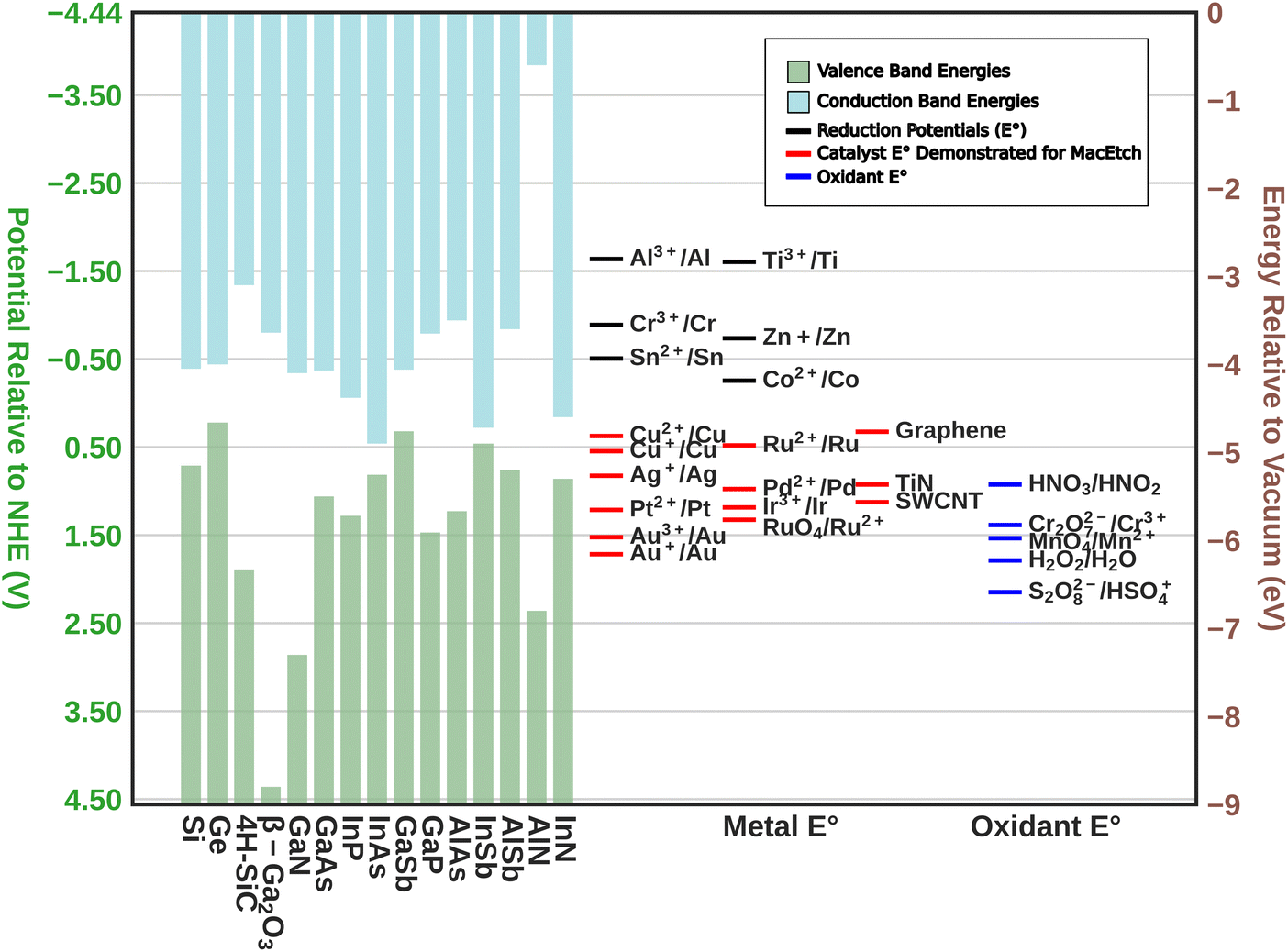 | ||
| Fig. 1 The upper band structure of semiconductors relative to the reduction potentials (E°) of common metals, catalysts demonstrated to promote MacEtch, and common oxidants. | ||
Several variations on the standard MacEtch process have been implemented to address fabrication challenges, either due to the material system or due to other specific constraints on final etch dimensions. These include: (a) photo-assisted MacEtch,34 which relies on photogenerated carriers to facilitate the MacEtch catalytic process; (b) magnetic MacEtch,15 in which superficial magnets direct the catalyst via magnetic field interactions; (c) self-anchored catalyst (SAC) MacEtch,35 in which designed holes in the catalyst layer anchor the catalyst to the substrate via physical forces and allow for the generation of deep, high aspect ratio features; (d) MacImprint,36 which utilizes a catalyst-coated polymer stamp to direct the etch in a controllable fashion and (e) anodic MacEtch,37 which proceeds by a two-step mechanism where holes are generated by an applied electrical current and are trapped at the catalyst–substrate interface by band bending.
Despite the differences between material systems, consideration of the oxidation reduction potentials of the substrate material alongside those of the oxidant, catalyst, and etchant, will provide a framework for the design of MacEtch systems for a given material (Fig. 1). This is aided by the construction of a conceptual oxidation ladder, on which charge carriers are transported to lower energies by moving between the substrate at high potential and the oxidant at low potential; all mediated by the interceding catalyst. Critical to this conceptualization is the ladder itself. A more negative oxidation potential relative to vacuum level will not always result in more aggressive etching, as evidenced by comparisons of etch rates between Pt and Au catalysts,28,38 but instead it is necessary for the catalyst to serve as an intermediary between etchant and substrate. If magnitude alone determined the etch rate, one would expect lone oxidant to etch faster than when catalyzed, shown not to be the case.26 It could be suggested a “gold”-ilocks zone for catalyst exists between the redox potential of the oxidant and the band edge of the catalyst, to foment a reduction ladder with equally spaced steps.
In this review, a survey of past MacEtch processes in materials aside from silicon is presented, beginning first with binary semiconductor etch systems and proceeding on to describing ternary alloys, before finally discussing other wide-bandgap semiconducting materials including those which have been demonstrated to be etchable through MacEtch. The body of research discussed herein demonstrates the wide-ranging utility of MacEtch to compound semiconductor processing and proposes a framework for consideration of MacEtch mechanisms during etching, including the conditions under which the necessary hole injection processes arise and what external conditions are necessary to drive the MacEtch mechanism. We also provide a repository of MacEtch recipes from the literature, which are intended to guide future research. There are considerable challenges confronting the implementation of MacEtch in many industrial settings, including the process compatibility of catalysts, the repeatability and uniformity of the process and the feature dimensions able to be generated. It is our intent that this review will serve as a reference for those tackling these challenges.
Background
MacEtch is believed to operate via a mechanism (Fig. 2) hinged on oxidation–reduction28 reactions between the two interfaces of the metal catalyst: the metal–solution interface and the metal–semiconductor interface, which act as cathode and anode, respectively.27 The metal layer catalyzes the oxidation of the semiconductor surface. The oxide generated by this process is then dissolved by oxide etchants present in solution, which access the interface via diffusion through adjacent oxidized semiconductor.26 The main mechanism by which MacEtch catalysis occurs is one of hole injection as the accumulation of charge in both the solution and the substrate leads to polarization along the interface as charges locally stabilize.39,40 The exchange can be understood as an electrochemical process with two localized half reactions.8,26,27 In the cathode reaction, interface polarization induced by the metal catalyst drives a carrier exchange as electrons are transported into the catalyst, holes are injected into the substrate and polarization grows. Simultaneously, a soluble complex forms under the catalyst and begins to dissolve in the anode reaction.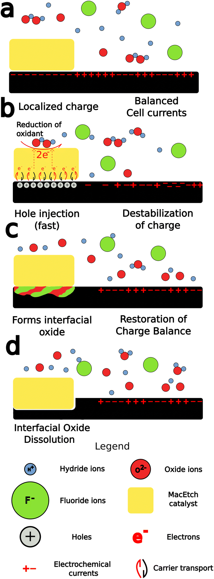 | ||
| Fig. 2 Forward MacEtch mechanism: (a) charge builds up along the metal–semiconductor interface; (b) reduction of oxidant at the metal injects holes into the semiconductor and results in destabilization of charge balance across the semiconductor; (c) oxidation by solution consumes the holes and restores charge neutrality; (d) surface oxide is dissolved and the substrate is etched, metal descends into the substrate. | ||
The progression and morphology of a MacEtch process depend on the reaction-limiting conditions during the etch.28 The level of solution access to the oxidized, catalyst-adjacent substrate, the lateral diffusion rate of injected holes, and the solubility of the intermediate interfacial species all influence the etch.1,10,26,33 If carrier generation or diffusion is limited at the catalyst–substrate interface, then the rate of hole injection into the semiconductor is less than the rate of hole consumption by the oxidation processes. As a result, the injected holes will rapidly oxidize the semiconductor, promoting the forward progression of MacEtch. Alternatively, if mass transport of oxidized material is the rate-limiting factor, for example, due to inadequate solution access to the oxidized semiconductor, then holes will diffuse to catalyst-adjacent regions before the interfacial material can be dissolved (Fig. 3). For such a case, the etch will proceed in regions without patterned catalyst, generating an “inverse” etch progression by comparison to the first case.26 In a separate I-MacEtch mechanism, if an insoluble, interfacial oxide develops at the catalyst-semiconductor interface, then holes that are not captured by oxidation processes will diffuse outward for oxidation at off-catalyst regions.10
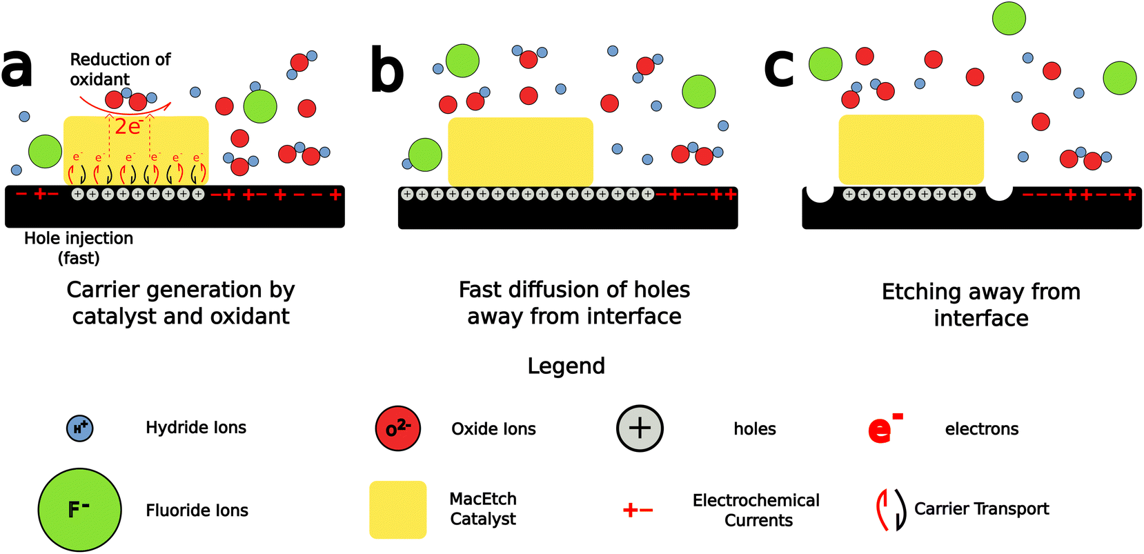 | ||
| Fig. 3 The general inverse progression MacEtch mechanism: (a) reduction of oxidant at the metal leads to hole injection at the semiconductor/metal interface; (b) holes diffuse away from the interface; (c) oxidized substrate is consumed by the solution. | ||
The MacEtch solution is composed of, at most essential, an oxidant and an acid etchant, but is often supplemented with a mobile surfactant to enhance mass transport of the etching reagents and products.27 The role of the oxidant is one of electron acceptor and hole generator. It often undergoes catalytic reduction at the metal, most importantly generating holes in the metal catalyst, but also decomposing in solution into either radical or negatively charged species prior to reacting with other aqueous species in the solution, or the substrate itself. When these nucleophilic species introduced into the solution react with the substrate, they often generate soluble byproducts, as is the case of hydrogen peroxide reaction with silicon to generate silicon oxide,41 which then proceeds to be dissolved in the highly acidic and electrophilic etch solution. This etch solution is made to attack the oxidized substrate due to the presence of the acid etchant in solution.40 These acid etchants when in solution are partially composed of highly electrophilic counteranions, which strip the oxidized species from the reactant surface, solubilizing them in the process.
While this process is well characterized for silicon, which has benefited from development and thorough study of oxide growth and the HF–silicon oxide etching chemistry, this is not the case for III–V materials, which develop their own oxide films with unique chemical properties.42 Additionally, the band gap energies vary greatly among the different semiconductor materials (Fig. 1), predisposing them to oxidation by different oxidants and under different conditions than those utilized for the catalytic etching of silicon. Further complicating matters is the compound nature of alloyed semiconductors, which requires two oxidation chemistries be considered during the dissolution step. This leads to a range of results, including the generation of crystalline deposits on the surface of MacEtched structures as the distinct oxide associated with each alloy is dissolved, precipitated, and redissolved.10,26,33
The most important features of MacEtch are appropriate charge generation and diffusion into the substrate, the formation of a soluble interfacial oxide, and the mass transport of solution species to and from the interface. Interfacial oxide solubility can be tuned, in some cases, by adjusting solution composition, but is also material dependent. Solution access, on the other hand, can be enhanced by controlling the process conditions during the fabrication of the metal catalyst.43 By restricting the metal thickness, holes will experience a greater potential for diffusion across the catalyst into the substrate. Similarly, by restricting the catalyst thickness to the extent it remains a porous material network and never coalesces to form a continuous film, solution access via the pores is permitted, increasing vertical etch rates and leaving behind high aspect ratio nanowires. This catalyst configuration is commonly referred to as the “self-anchored catalyst”.35 These nanowires can be cleared in post-etch processing to obtain the desired structure.
The MacEtch rate is known to especially depend on the diffusion and consumption rates of hole carriers in the semiconductor being etched. The catalytic film plays a dual role in facilitating etching. The first function is to catalyze the oxidative half reaction and inject holes into the substrate, the second being the formation of interfacial junctions leading to barriers or promoters of carrier diffusion, depending on band configurations at the interface.44 Band-bending arising from a Schottky barrier will impede hole diffusion away from the metal and restrict etching to the interfacial zones. Formation of an Ohmic junction with the substrate will promote hole diffusion away from the interface and increase the lateral etch rate.44 Oxidant concentration is also critical, as crystal progression45 and etch rate46 are both known to depend on MacEtch solution composition. Surface topography and retexturing during etching will thus vary depending on the semiconductor-catalyst etch system.
In n-type GaAs being etched with Au as the catalyst, for instance, the band bending generates a Schottky barrier, concentrating injected holes at the catalyst interface. This effect is evidenced by a reduced lateral etch rate in n-type GaAs and an oxidant concentration-dependent aspect ratio for GaAs pillars fabricated by MacEtch.21 Higher oxidant concentrations were shown to increase lateral etch rates and reduce fabricated aspect ratios due to increased hole injection during the dissolution step of MacEtch. The effect of the Schottky barrier on etch progression is further evidenced by the relationship between catalyst and etch rate observed for GaN MacEtch. Reduced Schottky barrier heights due to differences in catalyst work function will increase both the lateral etch rate and the overall etch rate as a result of increased hole injection and faster hole diffusion in the semiconductor.38 Schottky barrier height reductions in SiC arising due to dopant concentration changes lead to increases in etch porosity and depth.47
The ratio of lateral to vertical etch rate will determine the topography of the resulting etch features; however, the crystallinity of the substrate is generally preserved and only engraved by the catalyst. Preservation of substrate sidewall without the damage associated with dry etching is a hallmark of MacEtch. Transmission electron microscopy (TEM) studies have demonstrated the preservation of substrate crystallinity in Si.45 Under high oxidant concentration conditions, TEM analysis has demonstrated the generation of surface porosity in MacEtch-fabricated nanowires. However, under the most extreme etch conditions leading to the greatest degrees of surface porosity, the native Si crystallinity was still preserved, as demonstrated via selected-area electron diffraction (SAED) analysis.48 Moreover, h-MacEtch studies have shown that near-perfect elimination of non-vertical etch displacement is possible with MacEtch.15 TEM studies of InP17 and β-Ga2O333 have also demonstrated smooth sidewalls of MacEtch features where substrate crystallinity is preserved following etching.
GaAs
Gallium Arsenide (GaAs) is a III–V compound semiconductor with a direct bandgap (1.42 eV) and characteristic wavelength (857 nm) in the infrared range of the electromagnetic spectrum. GaAs possesses high electron mobility (8500 cm2 V−1 s−1), good thermal characteristics (conductivity 0.55 W cm−1 °C−1, diffusivity 0.31 cm2 s−1, linear expansion 5.73 × 10⁻⁶ °C−1) and a zinc blende configuration.49,50 Optical sensitivity in the near-infrared region, along with the stable crystal structure make GaAs ideal for many optoelectronic51–53 and photovoltaic54,55 devices, including near-IR photodetectors31,56 and optical waveguides57–60 operating at high enough temperatures to generate thermal carriers. The fabrication of GaAs nanoscale structures is regularly achieved with wet or dry etch techniques; however, there are advantages to MacEtch processing of GaAs for specific applications. MacEtch of GaAs is perhaps better realized in a different fashion to silicon MacEtch, however, as GaAs will isotropically wet etch in a HF/H2O2 solution without the presence of catalyst61–63 and peroxide-based catalytic etching will etch in undesirable crystallographic directions.61,64 This greatly limits the overall aspect ratio obtainable when using a hydrogen peroxide based solution; however, alterations to the solution chemistry have been shown to enable high aspect ratio MacEtch of GaAs structures. Employing KMnO4 as oxidant was shown to improve MacEtch outcomes in GaAs.21,63 The etch rate in potassium permanganate is directly influenced by the interaction between the electronic band structure of GaAs and that of the catalyst. For Au catalysts contacted to n-type GaAs, the Schottky barrier at the interface bends the band upwards, trapping hole carriers at the interface and promoting forward progression of MacEtch.44 The published results on MacEtch research are listed below in Table 1, with respect to etching conditions and dimensions of the MacEtch-fabricated structures.| Ref. | Temp | Dop | Cat Mat'l | Cat Th (nm) | Ox. | Etch | Sur | Ox (M) | Etch (M) | Molar ratio (Etch/Ox) | Surf Vol (mL) | Total Vol (mL) | Prog | Etch depth (μm) | Etch Rate (μm min−1) | Features | Feat width (μm) |
|---|---|---|---|---|---|---|---|---|---|---|---|---|---|---|---|---|---|
| Key: Ref. – reference number, Temp. – temperature, RT – room temperature, Dop. – doping type, Cat. – catalyst, Mat'l – Material, Th. – thickness, semins- semi-insulating, intrins. – intrinsic, Ox. – oxidant, Etch. – etchant, Surf. – surfactant, Vol. – volume, Prog. – Progression, Fwd. – Forward, Inv. – Inverse, Imp. – Imprint. | |||||||||||||||||
| 65 | 298 K | n-type | CuSO4 | H2O2 | HF | 1 | 5 | 5 | 0 | 0 | |||||||
| 298 K | n-type | AgClO4 | H2O2 | HF | 1 | 5 | 5 | Fwd | 0.035 | 0.035 | Nanopillars | 1 | |||||
| 66 | RT | n-type | CuSO4 | H2O2 | HF | 1 | 5 | 5 | |||||||||
| n-type | AgClO4 | H2O2 | HF | 1 | 5 | 5 | Fwd | 0.035 | 0.035 | Nanopillars | 1 | ||||||
| n-type | PdCl2 | H2O2 | HF | 1 | 5 | 5 | Fwd | 0.17 | 2.04 | Nanopillars | |||||||
| 64 | RT | n-type | Au | 6 | H2O2 | HF | 1 | 5 | 5 | Fwd | .25 | .25 | Micropillars | 3 | |||
| 67 | RT | n-type | Pt/Pd | 6 | H2O2 | HF | 1 | 7.5 | 7.5 | Fwd | 0.9 | 0.9 | Microholes | 1–3 | |||
| Au | 20 | H2O2 | HF | 1 | 5 | 5 | Fwd | 1.4 | 1.4 | Microholes | |||||||
| 61 | RT | n-type | Pt/Pd | 5 | H2O2 | HF | 1 | 5 | 5 | Fwd | 0.67 | 0.67 | Microholes, micropillars | 3 | |||
| 1 | 7.5 | 0.14 | Fwd | 0.9 | 0.9 | ||||||||||||
| 63 | RT | n-type | Au | 20 | KMnO4 | HF | H2O | 0.02 | Fwd | 0.82 | 0.27 | Squares | 300 | ||||
| n-type | Au | 20 | KMnO4 | HF | H2O | 0.04 | Fwd | 4.14 | 1.38 | Squares | 300 | ||||||
| n-type | Au | 2 | KMnO4 | HF | H2O | 0.05 | Fwd | 1.92 | 0.64 | Squares | 300 | ||||||
| n-type | Au | 20 | KMnO4 | HF | H2O | 0.065 | Fwd | 1.78 | 0.59 | Squares | 300 | ||||||
| n-type | Au | 20 | KMnO4 | HF | H2O | 0.09 | Fwd | 2.10 | 0.70 | Squares | 300 | ||||||
| 40–5 °C | n-type | Au | 20 | KMnO4 | H2SO4 | H2O | “sat." | Fwd | Square mesh | 0.6 | |||||||
| 30–5 °C | n-type | Au | 2 | KMnO4 | H2SO4 | H2O | "sat." | Inv | Square mesh | 0.6 | |||||||
| RT | n-type | Au | 20 | KMnO4 | HF | H2O | 0.056 | Square mesh | 1 | ||||||||
| 68 | n-type | Au | 20 | H2O2 | HF | 1 | 3–5 | 3–5 | Fwd | 1.2 | 1.2 | Microholes | ∼1.5 | ||||
| 69 | 45 °C | n-type | Au | 20 | KMnO4 | H2SO4 | H2O | 0.005 | 1.84 | 368.0 | Fwd | 0.98 | 0.196 | Stripes | 2 | ||
| 45 °C | n-type | Au | 20 | KMnO4 | H2SO4 | H2O | 0.010 | 1.84 | 184.0 | Fwd | 1.47 | 0.294 | Stripes | 2 | |||
| 45 °C | n-type | Au | 20 | KMnO4 | H2SO4 | H2O | 0.015 | 1.84 | 122.7 | Fwd | 3.94 | 0.788 | Stripes | 2 | |||
| 45 °C | n-type | Au | 20 | KMnO4 | H2SO4 | H2O | 0.005 | 1.84 | 368.0 | Fwd | 0.5 | 0.1 | Stripes | 5 | |||
| 45 °C | n-type | Au | 20 | KMnO4 | H2SO4 | H2O | 0.010 | 1.84 | 184.0 | Fwd | 0.9 | 0.18 | Stripes | 5 | |||
| 45 °C | n-type | Au | 20 | KMnO4 | H2SO4 | H2O | 0.015 | 1.84 | 122.7 | Fwd | 1.61 | 0.322 | Stripes | 5 | |||
| 45 °C | n-type | Au | 20 | KMnO4 | H2SO4 | H2O | 0.005 | 1.84 | 368.0 | Fwd | 0.28 | 0.056 | Stripes | 56 | |||
| 45 °C | n-type | Au | 20 | KMnO4 | H2SO4 | H2O | 0.010 | 1.84 | 184.0 | Fwd | 0.76 | 0.152 | Stripes | 56 | |||
| 45 °C | n-type | Au | 20 | KMnO4 | H2SO4 | H2O | 0.015 | 1.84 | 122.7 | Fwd | 1.76 | 0.352 | Stripes | 56 | |||
| 55 °C | n-type | Au | 20 | KMnO4 | H2SO4 | H2O | 0.005 | 1.84 | 368.0 | Fwd | Stripes | 2 | |||||
| 55 °C | n-type | Au | 20 | KMnO4 | H2SO4 | H2O | 0.010 | 1.84 | 184.0 | Fwd | Stripes | 2 | |||||
| 55 °C | n-type | Au | 20 | KMnO4 | H2SO4 | H2O | 0.015 | 1.84 | 122.7 | Fwd | Stripes | 2 | |||||
| 55 °C | n-type | Au | 20 | KMnO4 | H2SO4 | H2O | 0.005 | 1.84 | 368.0 | Fwd | Stripes | 5 | |||||
| 55 °C | n-type | Au | 20 | KMnO4 | H2SO4 | H2O | 0.010 | 1.84 | 184.0 | Fwd | Stripes | 5 | |||||
| 55 °C | n-type | Au | 20 | KMnO4 | H2SO4 | H2O | 0.015 | 1.84 | 122.7 | Fwd | Stripes | 5 | |||||
| 55 °C | n-type | Au | 20 | KMnO4 | H2SO4 | H2O | 0.005 | 1.84 | 368.0 | Fwd | Stripes | 56 | |||||
| 55 °C | n-type | Au | 20 | KMnO4 | H2SO4 | H2O | 0.010 | 1.84 | 184.0 | Fwd | Stripes | 56 | |||||
| 55 °C | n-type | Au | 20 | KMnO4 | H2SO4 | H2O | 0.015 | 1.84 | 122.7 | Fwd | Stripes | 56 | |||||
| 35 °C | n-type | Au | 20 | KMnO4 | H2SO4 | H2O | 0.005 | 1.84 | 368.0 | Fwd | Stripes | 2 | |||||
| 35 °C | n-type | Au | 20 | KMnO4 | H2SO4 | H2O | 0.010 | 1.84 | 184.0 | Fwd | Stripes | 2 | |||||
| 35 °C | n-type | Au | 20 | KMnO4 | H2SO4 | H2O | 0.015 | 1.84 | 122.7 | Fwd | Stripes | 2 | |||||
| 35 °C | n-type | Au | 20 | KMnO4 | H2SO4 | H2O | 0.005 | 1.84 | 368.0 | Fwd | Stripes | 5 | |||||
| 35 °C | n-type | Au | 20 | KMnO4 | H2SO4 | H2O | 0.010 | 1.84 | 184.0 | Fwd | Stripes | 5 | |||||
| 35 °C | n-type | Au | 20 | KMnO4 | H2SO4 | H2O | 0.015 | 1.84 | 122.7 | Fwd | stripes | 5 | |||||
| 35 °C | n-type | Au | 20 | KMnO4 | H2SO4 | H2O | 0.005 | 1.84 | 368.0 | Fwd | Stripes | 56 | |||||
| 35 °C | n-type | Au | 20 | KMnO4 | H2SO4 | H2O | 0.010 | 1.84 | 184.0 | Fwd | Stripes | 56 | |||||
| 35 °C | n-type | Au | 20 | KMnO4 | H2SO4 | H2O | 0.015 | 1.84 | 122.7 | Fwd | Stripes | 56 | |||||
| 25 °C | n-type | Au | 20 | KMnO4 | H2SO4 | H2O | 0.005 | 1.84 | 368.0 | Fwd | Stripes | 2 | |||||
| 25 °C | n-type | Au | 20 | KMnO4 | H2SO4 | H2O | 0.010 | 1.84 | 184.0 | Fwd | Stripes | 2 | |||||
| 25 °C | n-type | Au | 20 | KMnO4 | H2SO4 | H2O | 0.015 | 1.84 | 122.7 | Fwd | Stripes | 2 | |||||
| 25 °C | n-type | Au | 20 | KMnO4 | H2SO4 | H2O | 0.005 | 1.84 | 368.0 | Fwd | Stripes | 5 | |||||
| 25 °C | n-type | Au | 20 | KMnO4 | H2SO4 | H2O | 0.010 | 1.84 | 184.0 | Fwd | Stripes | 5 | |||||
| 25 °C | n-type | Au | 20 | KMnO4 | H2SO4 | H2O | 0.015 | 1.84 | 122.7 | Fwd | Stripes | 5 | |||||
| 25 °C | n-type | Au | 20 | KMnO4 | H2SO4 | H2O | 0.005 | 1.84 | 368.0 | Fwd | Stripes | 56 | |||||
| 25 °C | n-type | Au | 20 | KMnO4 | H2SO4 | H2O | 0.010 | 1.84 | 184.0 | Fwd | Stripes | 56 | |||||
| 25 °C | n-type | Au | 20 | KMnO4 | H2SO4 | H2O | 0.015 | 1.84 | 122.7 | Fwd | Stripes | 56 | |||||
| 70 | 40 °C | n-type | Au | 20 | KMnO4 | H2SO4 | H2O | Inv | Dots | 1.4–2.5 | |||||||
| 40 °C | n-type | Au | 20 | KMnO4 | H2SO4 | H2O | Inv | Stripes | 1.1–2 | ||||||||
| 40 °C | n-type | Au | 20 | KMnO4 | H2SO4 | H2O | Inv | Mesh | 2–8 | ||||||||
| 45 °C | n-type | Au | 20 | KMnO4 | H2SO4 | H2O | Inv | Dots | 1.4–2.5 | ||||||||
| 45 °C | n-type | Au | 20 | KMnO4 | H2SO4 | H2O | Inv | Stripes | 1.1–2 | ||||||||
| 45 °C | n-type | Au | 20 | KMnO4 | H2SO4 | H2O | Inv | Mesh | 2–8 | ||||||||
| 50 °C | n-type | Au | 20 | KMnO4 | H2SO4 | H2O | Fwd | Dots | 1.4–2.5 | ||||||||
| 50 °C | n-type | Au | 20 | KMnO4 | H2SO4 | H2O | Fwd | Stripes | 1.1–2 | ||||||||
| 50 °C | n-type | Au | 20 | KMnO4 | H2SO4 | H2O | Fwd | Mesh | 2–8 | ||||||||
| 71 | 35 °C | n-type | KMnO4 | H2SO4 | H2O | 5 | 0.07 | 0.014 | 100 | 3.4 | 0.11 | Lines | 8 | ||||
| 35 °C | n-type | Au | 30 | KMnO4 | H2SO4 | H2O | 5 | 0.07 | 0.014 | 100 | 6 | 0.2 | Squares | 12 | |||
| 35 °C | n-type | Au | 30 | KMnO4 | H2SO4 | H2O | 5 | 0.07 | 0.014 | 100 | 6 | 0.2 | Lines | 8 | |||
| 45 °C | n-type | Au | 30 | KMnO4 | H2SO4 | H2O | 5 | 0.07 | 0.014 | 100 | 1.8 | 0.18 | Lines | 4 | |||
| 72 | 45 °C | n-type | Au | 30 | KMnO4 | HF | 0.001 | 20 | 20![[thin space (1/6-em)]](https://www.rsc.org/images/entities/char_2009.gif) 000 000 |
Fwd | Nanodots | 70 | |||||
| 45 °C | n-type | Au | 30 | KMnO4 | HF | 0.01 | 5 | 500 | Inv | Nanopillars | 70 | ||||||
| 45 °C | n-type | Au | 30 | KMnO4 | HF | 0.01 | 10 | 1000 | Inv | Nanopillars | 70 | ||||||
| 45 °C | n-type | Au | 30 | KMnO4 | HF | 0.01 | 20 | 2000 | Inv | Nanopillars | 70 | ||||||
| 20 °C | n-type | Au | 30 | KMnO4 | HF | 0.01 | 5 | 500 | Inv | Nanopillars | 70 | ||||||
| 20 °C | n-type | Au | 30 | KMnO4 | HF | 0.01 | 10 | 1000 | Inv | Nanopillars | 70 | ||||||
| 20 °C | n-type | Au | 30 | KMnO4 | HF | 0.01 | 20 | 2000 | Inv | 0.05 | 0.3 | Nanopillars | 70 | ||||
| 62 | n-type | Au | 20 | KMnO4 | HF | EtOH | 0.005 | 14 | 2800 | 20 | 40 | Fwd | 0.5–1.2 | Nanopillars | 0.6 | ||
| 73 | n-type | Au | H2O2 | HF | 4 | Inv | 5.5 | 0.55 | Black GaAs | ||||||||
| 74 | RT | semins | Au | KMnO4 | HF | 0.011 | 14.07 | 1334.9 | Fwd | 2.11 | Nanowires | 325 | |||||
| RT | semins | Au | KMnO4 | HF | 0.011 | 14.07 | 1334.9 | Fwd | 2.38 | Nanowires | 170 | ||||||
| 21 | RT | p-type | Au | 35 | KMnO4 | HF | H2O | 0.005 | 0.42 | 26.57 | 15 | 30 | Fwd | 1.8 | 0.60 | Square mesh | 1000 |
| 0 °C | n-type | Au | 35 | KMnO4 | HF | H2O | 0.011 | 0.42 | 13.27 | 15 | 30 | Fwd | 0.63 | 0.063 | Square grid | 1000 | |
| intrins. | Au | 35 | KMnO4 | HF | H2O | 0.011 | 0.42 | 13.27 | 15 | 30 | Fwd | 0.53 | 0.053 | Square grid | 1000 | ||
| p-type | Au | 35 | KMnO4 | HF | H2O | 0.011 | 0.42 | 13.27 | 15 | 30 | Fwd | 2.53 | 0.253 | Square grid | 1000 | ||
| 20 °C | n-type | Au | 35 | KMnO4 | HF | H2O | 0.011 | 0.42 | 13.27 | 15 | 30 | Fwd | 1.4 | 0.14 | Square grid | 1000 | |
| intrins. | Au | 35 | KMnO4 | HF | H2O | 0.011 | 0.42 | 13.27 | 15 | 30 | Fwd | 1.3 | 0.13 | Square grid | 1000 | ||
| p-type | Au | 35 | KMnO4 | HF | H2O | 0.011 | 0.42 | 13.27 | 15 | 30 | Fwd | 3.18 | 0.318 | Square grid | 1000 | ||
| 40 °C | n-type | Au | 35 | KMnO4 | HF | H2O | 0.011 | 0.42 | 13.27 | 15 | 30 | Fwd | 2.56 | 0.256 | Square grid | 1000 | |
| intrins | Au | 35 | KMnO4 | HF | H2O | 0.011 | 0.42 | 13.27 | 15 | 30 | Fwd | 2.67 | 0.267 | Square grid | 1000 | ||
| p-type | Au | 35 | KMnO4 | HF | H2O | 0.011 | 0.42 | 13.27 | 15 | 30 | Fwd | 3.47 | 0.347 | Square grid | 1000 | ||
| 60 °C | n-type | Au | 35 | KMnO4 | HF | H2O | 0.011 | 0.42 | 13.27 | 15 | 30 | Fwd | 2.43 | 0.243 | Square grid | 1000 | |
| intrins | Au | 35 | KMnO4 | HF | H2O | 0.011 | 0.42 | 13.27 | 15 | 30 | Fwd | 2.61 | 0.261 | Square grid | 1000 | ||
| p-type | Au | 35 | KMnO4 | HF | H2O | 0.011 | 0.42 | 13.27 | 15 | 30 | Fwd | 3.33 | 0.333 | Square grid | 1000 | ||
| RT | n-type | Au | 35 | KMnO4 | HF | H2O | 0.011 | 0.14 | 4.45 | 24 | 30 | Fwd | 0.18 | 0.018 | Square grid | 1000 | |
| intrins | Au | 35 | KMnO4 | HF | H2O | 0.011 | 0.14 | 4.45 | 24 | 30 | Fwd | 0.43 | 0.043 | Square grid | 1000 | ||
| p-type | Au | 35 | KMnO4 | HF | H2O | 0.011 | 0.14 | 4.45 | 24 | 30 | Fwd | 1.02 | 0.102 | Square grid | 1000 | ||
| RT | n-type | Au | 35 | KMnO4 | HF | H2O | 0.011 | 0.28 | 8.82 | 20 | 30 | Fwd | 0.87 | 0.087 | Square grid | 1000 | |
| intrins | Au | 35 | KMnO4 | HF | H2O | 0.011 | 0.28 | 8.82 | 20 | 30 | Fwd | 0.51 | 0.051 | Square grid | 1000 | ||
| p-type | Au | 35 | KMnO4 | HF | H2O | 0.011 | 0.28 | 8.82 | 20 | 30 | Fwd | 2.7 | 0.27 | Square grid | 1000 | ||
| RT | n-type | Au | 35 | KMnO4 | HF | H2O | 0.011 | 0.42 | 13.27 | 15 | 30 | Fwd | 1.86 | 0.186 | Square grid | 1000 | |
| intrins | Au | 35 | KMnO4 | HF | H2O | 0.011 | 0.42 | 13.27 | 15 | 30 | Fwd | 1.76 | 0.176 | Square grid | 1000 | ||
| p-type | Au | 35 | KMnO4 | HF | H2O | 0.011 | 0.42 | 13.27 | 15 | 30 | Fwd | 3.65 | 0.365 | Square grid | 1000 | ||
| RT | n-type | Au | 35 | KMnO4 | HF | H2O | 0.011 | 0.56 | 17.73 | 10 | 30 | Fwd | 1.76 | 0.176 | Square grid | 1000 | |
| intrins | Au | 35 | KMnO4 | HF | H2O | 0.011 | 0.56 | 17.73 | 10 | 30 | Fwd | 1.58 | 0.158 | Square grid | 1000 | ||
| p-type | Au | 35 | KMnO4 | HF | H2O | 0.011 | 0.56 | 17.73 | 10 | 30 | Fwd | 4.69 | 0.469 | Square grid | 1000 | ||
| RT | n-type | Au | 35 | KMnO4 | HF | H2O | 0.011 | 0.70 | 22.09 | 6 | 30 | Fwd | 0 | 0 | Square grid | 1000 | |
| intrins | Au | 35 | KMnO4 | HF | H2O | 0.011 | 0.70 | 22.09 | 6 | 30 | Fwd | 0 | 0 | Square grid | 1000 | ||
| p-type | Au | 35 | KMnO4 | HF | H2O | 0.011 | 0.70 | 22.09 | 6 | 30 | Fwd | 0.82 | 0.082 | Square grid | 1000 | ||
| RT | n-type | Au | 35 | KMnO4 | HF | H2O | 0.005 | 0.56 | 35.48 | 10 | 30 | Fwd | 0.59 | 0.059 | Square grid | 1000 | |
| intrins | Au | 35 | KMnO4 | HF | H2O | 0.005 | 0.56 | 35.48 | 10 | 30 | Fwd | 0.59 | 0.059 | Square grid | 1000 | ||
| p-type | Au | 35 | KMnO4 | HF | H2O | 0.005 | 0.56 | 35.48 | 10 | 30 | Fwd | 1.77 | 0.177 | Square grid | 1000 | ||
| RT | n-type | Au | 35 | KMnO4 | HF | H2O | 0.021 | 0.56 | 8.86 | 10 | 30 | Fwd | 4.36 | 0.436 | Square grid | 1000 | |
| intrins | Au | 35 | KMnO4 | HF | H2O | 0.021 | 0.56 | 8.86 | 10 | 30 | Fwd | 4.36 | 0.436 | Square grid | 1000 | ||
| p-type | Au | 35 | KMnO4 | HF | H2O | 0.021 | 0.56 | 8.86 | 10 | 30 | Fwd | 10.97 | 1.097 | Square grid | 1000 | ||
| RT | n-type | Au | 35 | KMnO4 | HF | H2O | 0.031 | 0.56 | 5.91 | 10 | 30 | Fwd | 6.01 | 0.601 | Square grid | 1000 | |
| intrins | Au | 35 | KMnO4 | HF | H2O | 0.031 | 0.56 | 5.91 | 10 | 30 | Fwd | 6.01 | 0.601 | Square grid | 1000 | ||
| p-type | Au | 35 | KMnO4 | HF | H2O | 0.031 | 0.56 | 5.91 | 10 | 30 | Fwd | 14.62 | 1.462 | Square grid | 1000 | ||
| RT | n-type | Au | 35 | KMnO4 | HF | H2O | 0.042 | 0.56 | 4.43 | 10 | 30 | Fwd | 8.49 | 0.849 | Square grid | 1000 | |
| intrins | Au | 35 | KMnO4 | HF | H2O | 0.042 | 0.56 | 4.43 | 10 | 30 | Fwd | 9.43 | 0.943 | Square grid | 1000 | ||
| p-type | Au | 35 | KMnO4 | HF | H2O | 0.042 | 0.56 | 4.43 | 10 | 30 | Fwd | 21.82 | 2.182 | Square grid | 1000 | ||
| 22 | semins | Au | 30 | KMnO4 | HF | H2O | 0.005 | 15 | 15 | Fwd | 1 | 0.118 | Hole array | 0.77 | |||
| 75 | 35–7 °C | n-type | Pt | 100 | KMnO4 | H2SO4 | 0.04 | 1.84 | 0.022 | Imp | 1 | 0.066 | Squares | 2–5 | |||
| 76 | 35–7 °C | n-type | Pt | 100 | KMnO4 | H2SO4 | 0.04 | Imp | 0.5 | 0.025 | 3D-MNS | ||||||
| 77 | n-type | Au | 100 | KMnO4 | HF | H2O | 0.011–21 | 14 | 667–1333 | 15 | 30 | Imp | 1 | 0.4 | MULTIPLE | ||
| 78 | 35–7 °C | n-type | Pt | 100 | KMnO4 | H2SO4 | 0.04 | 1.84 | 45.4 | Imp | 1.33 | 3D-MNS | 0.5 | ||||
| 79 | n-type | Pt | KMnO4 | H2SO4 | 0.005–0.06 | 1.84 | 33–333 | Imp | 4.2 | 0.1 | Array | 4 | |||||
| 80 | n-type | Pt | KMnO4 | H2SO4 | 1.84 | 1.84 | 1 | Imp | 2.6 | 0.13 | Array | 7.4 | |||||
In 2008, Yasukawa et al.65 demonstrated forward MacEtch of n-type GaAs with a HF and H2O2 solution. The wafer was patterned by nanosphere lithography and electroless wet Ag deposition formed the catalytic mask to etch pillars 35 nm high. Cu was also explored as catalyst, but unlike recent work where Cu was employed as a viable catalyst,81,82 Yasukawa et al. found no catalytic effect of Cu and observed only conventional, acatalytic wet etching. Etching was found to proceed faster in the 〈100〉 direction by comparison with the 〈111〉.
Yasukawa et al.66 went on to investigate the effect of different metals, either Cu, Ag or Pd, as catalysts for GaAs MacEtch in a HF and H2O2 solution. Cu was again found to exhibit no catalytic effect. Ag catalyzed the formation of micropillar arrays 1 μm diameter and 35 nm deep. Pd was also shown to catalyze forward MacEtch, at a 50× faster rate; however, the lateral etch rate was more than Ag leading to polishing at long etch times. This is likely due to greater Pd reduction potential generating more holes able to diffuse off-metal. Etching with and without catalyst was shown to prefer the 〈100〉 over the 〈111〉 direction.
Yasukawa et al.64 further investigated Au as an n-GaAs MacEtch catalyst in an effort to improve uniformity and anisotropy over the group's previous work. After nanosphere lithography to generate a 3 μm pillar pattern, 6 nm Au was deposited via ion sputtering and etching in HF/H2O2 solution proceeded. The etch rate in the 〈111〉 direction was shown faster than 〈100〉, but the lateral etch rate was also increased in 〈111〉 substrates. The uniformity of features was shown to be improved for sputtered catalyst by comparison with electroless wet deposited catalyst.
Yasukawa et al.67 compared Au and Pt/Pd catalysts deposited via ion sputtering and etched in a HF/H2O2 solution Nanospheres were used to generate catalyst microdots and samples were etched for 60 s (Fig. 4a). Results indicated Au to etch at a faster rate and with greater anisotropy, whereas Pt/Pd exhibited a preferential etch rate for the 〈111〉 direction over the 〈100〉 direction.
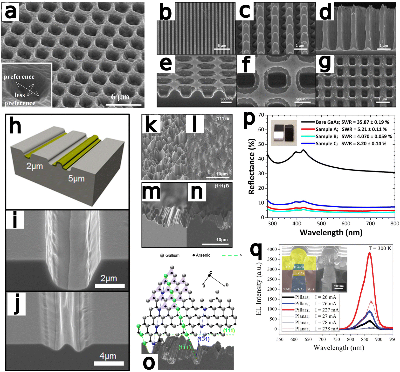 | ||
| Fig. 4 (a) Au-catalyzed hole formation after MacEtch of GaAs with inset displaying the preferential direction of etch progression. Reproduced from ref. 67 with permission of IOP Publishing, copyright 2009. (b–g) An identical Au catalyst pattern was defined on two GaAs substrates prior to MacEtch processing under different conditions. Independently, forward progression MacEtch (b–d) and inverse progression MacEtch (e–g) proceeded due to tuning of the etch conditions. Reproduced from ref. 63 with permission from American Chemical Society, copyright 2011. (h) The effect of pattern dimension on GaAs MacEtch progression in a KMnO4 solution was evaluated for (i) 2 and (j) 5 μm stripe thickness. Reproduced from ref. 69 with permission from American Chemical Society, copyright 2014. (k–o) Preferential etch planes for (111)B GaAs surfaces and effect on surface texturing. Reproduced from ref. 73 with permission from American Chemical Society, copyright 2018. (p) Reflectance enhancements in GaAs nanowires fabricated by MacEtch. Reproduced from ref. 74 with permission of IOP Publishing, copyright 2019. (q) Electroluminescence testing of p–i-n LED fabricated by HF/KMnO4/H2O MacEtch of GaAs pillars. MacEtch of GaAs was shown to enhance luminescent intensity by as much as 3 times. Reproduced from ref. 21 with permission from AIP Publishing, copyright 2013. | ||
Yasukawa et al.61 found Pt/Pd catalyst to etch faster than other catalysts tested (Ag, Pd, and Au.) Using nanosphere lithography, honeycomb and microdot catalyst patterns were fabricated on n-GaAs with 3 μm feature size. Substrates were etched in HF/H2O2 solution and etch rate was found to increase with increasing HF concentration. In off-metal regions, striped etching patterns formed due to anisotropic chemical etching of GaAs in absence of catalyst. The etch rate of chemical wet etching was 40× lower than the catalyzed etching. Feature shapes were elongated due to the honeycomb shape of the pattern, producing hotspots where metal regions are closer and other regions where the nearest metal neighbor is more distant. This leads to non-uniform hole accumulation profiles and results in variations in lateral etch rates.
DeJarld et al.63 showed forward progression (Fig. 4b–d) of GaAs MacEtch via the utilization of potassium permanganate as the oxidant reagent to achieve an aspect ratio greater than 10. DeJarld etched 〈100〉 GaAs substrate by depositing a gold mesh system via evaporation through a SiN hard-mask. DeJarld found that due to the bandgap offset of GaAs relative to the vacuum level, using hydrogen peroxide as the oxidant would not result in catalytic activity due to the high redox potential of peroxide (1.763 V vs. SHE) when compared to the work function of GaAs (0.25 V vs. SHE). KMnO4 (1.51 V vs. SHE) as oxidant in the MacEtch solution reduced the energy barrier to hole injection via the gold catalyst (0.66 V vs. SHE) while maintaining a barrier to etching in off metal areas. Sulfuric acid and hydrofluoric acid were employed as acid etchants in the solution system. Cautionary note: KMnO4 and sulfuric acid react exothermically and are potentially dangerous. DeJarld showed the effect of oxidant potential and concentration on etch selectivity and etch ratio as well as the influence of the pattern dimensions over the vertical to lateral etch ratio and the final aspect ratio produced. For large catalyst pattern sizes, etching occurred mainly at the boundaries of the pattern, with limited etching occurring below the center of the metal regions due to limited solution access to the region. By varying the oxidant concentration, vertical etch rate was found to increase with increased KMnO4 concentration up to a saturation level before plateauing. Lateral etching at high KMnO4 concentrations were found to overwhelm the vertical etch rate and produce a polishing effect with small feature sizes, by etching a lateral domain greater than one-half the spaces between features. Inverse progression MacEtch (Fig. 4e–g) was also demonstrated via a temperature dependent mechanism. DeJarld found forward progression to proceed between 40 and 45 °C for forward MacEtch, and inverse MacEtch at a range of 30 to 35 °C. Additional experiments examined MacEtch with a HF/KMnO4 solution in a borosilicate container, small changes in temperature and the over saturation of KMnO4 in sulfuric acid.
Yasukawa et al.68 investigated the formation of hole arrays in GaAs with Au catalyst and HF/H2O2 MacEtch solution. Au was found to facilitate more control over etch dimensions than Ag and Pt–Pd; however, the peroxide based solution resulted in a higher degree of crystallographic and acatalytic etching than a permanganate based solution regardless of catalyst. Due to the crystallographic dependence of etch rate in HF/H2O2 MacEtch solution, the orientation of the metal catalyst pattern relative to the substrate crystal resulted in rectangular holes assembled in one of two different formations: hexagonal close-packed and a vertically-aligned hole arrays.
In Cheung et al.,69 the effect of catalyst dimensions on the vertical selectivity of the etch rate were measured with MacEtch in a H2SO4 (18.4 M diluted to 10% in H2O), KMnO4 and H2O solution (Fig. 4h–j). Cautionary note: reaction of KMnO4 with H2SO4 is highly exothermic. Critically, oxidation of GaAs is comparatively easier than oxidation in silicon, and where silicon does not etch in the presence of peroxide without a catalyst, GaAs will etch with peroxide alone.83 This will produce a steady off-metal etch process which will affect finally topology. Cheung, as others, argued potassium permanganate as the less aggressive oxidant will significantly reduce the off-metal etch rate and better preserve the catalytic effect. By varying etchant concentrations (5–15 mM) with different Au film patterns to characterize the effect of the oxidant and catalyst, the vertical and lateral etch rate were determined to change with respect to oxidant concentration. The catalyst width exerted a greater overall effect on the etch ratio, however, with parachuting of the catalyst in wide dimension patterns due to preferential etching at the edges. Solution access to the region under the metal seemed to extend only to a distance of 1 μm, and patterns with greater than 2 μm width experienced a quenching of solution access to the center of the etched feature. High aspect ratio etching was achievable for feature sizes below 2 μm where hole diffusion did not exceed solution access. Temperature increases were shown to accelerate the vertical etch rate, at the cost of decreased sidewall smoothness, as the increased kinetics of higher temperatures lead to more ready migration of the catalyst. The etch rate increased with temperature until the more rapid H2 bubble formation delaminated the catalyst and prevented further etching.
Song and Oh70 achieved inverse progression MacEtch and the generation of porous GaAs in the region immediately adjacent to a deposited Au pattern at temperatures of 40 and 45 °C. At higher temperatures of 50 °C, they observed below-metal forward etching in the fabrication of high aspect ratio nanopillars.
Asoh et al.71 designed an experiment to control the front-side etch direction via backside deposition of the metal catalyst. The process flow involved patterning the frontside with a photoresist pattern and depositing gold films of up to 30 nm thickness onto the backside of a 450 μm substrate prior to MacEtch in a KMnO4 and H2SO4 solution. Cautionary note: reaction of KMnO4 with H2SO4 is highly exothermic. MacEtch with deposited backside catalyst proceeded at a faster rate than without a backside catalyst. The backside deposition of gold catalyst did not improve the lateral etch rate, suggesting the hole injection at the catalyst saturates the substrate with charge carriers across the whole thickness and drives the oxidation process without establishing a vertical gradient of hole concentration in the wafer. The process is advantageous for producing a gold-free wafer front side as the catalyst is only present on the backside. The wet etching of GaAs wafers in sulfuric acid and potassium permanganate without a metal catalyst and resist pattern only was employed to study the non-catalytic etching of the substrate. To determine isotropy, (100) and (111) crystal orientation GaAs wafers were studied under the same conditions, with the etched cross-sections containing an etched line pattern with a trapezoidal cross-section as a gradual lateral etch produces a curved sidewall surface. Etching was found to proceed faster in (111) wafers than (100).
Asoh et al.72 developed a vertical etching technique for 〈100〉 GaAs with low oxidant concentration and HF in the etchant solution. A gold catalyst was evaporated through an anodic aluminum oxide mask. The oxidant concentration was reduced to decrease the lateral etch rate and produce more vertical features. By reducing oxidant concentration at sufficiently high temperature, the MacEtch progression was shown to proceed in the forward regime and high aspect ratio features were fabricated according to the catalyst pattern. At higher oxidant concentrations, the rate of hole injection exceeded the rate of hole consumption; excess holes diffused outward from under the catalyst and to be etched by the solution, leading to inverse etching. At high oxidant and etchant concentrations, the catalyst mask was found to delaminate due to the high lateral etch rate.
Cowley et al.62 etched 600 nm diameter GaAs nanopillars to a depth up to 1.2 μm via nanosphere lithography and a KMnO4, HF, and ethanol MacEtch solution. Variation in etch rate was observed across the sample, with etch depths ranging from 0.5 to 1.2 μm. Delamination of the Au catalyst was prevented by a surfactant prewetting step before Au deposition, and variation in catalyst interface is suggested to explain the range of etch rates observed. Photoluminescence measurements observed 3× enhancement in intensity and a redshift of 3 nm in the luminescence wavelength. Additionally, Raman spectroscopic measurements indicated the presence of amorphous and crystalline As species at the interface alongside β-Ga2O3. It is suggested As may be undergoing transition from the amorphous to crystalline phase during etching. Lacking As2O3 signatures in the Raman trace is presented as evidence for an As-oxidation mediated MacEtch mechanism, previously proposed for GaAs etching.84,85
Lova et al.73 fabricated porous GaAs of a range of crystal orientations with a two-step MacEtch process. Solution deposition of 0.1 mM AuCl3 in water to form a Au nanoparticle catalyst preceded etching in a H2O2 and HF solution. The generation of porous regions in the GaAs substrate preceded along microfacets of crystal orientation, providing evidence for an orientation dependent etch rate (Fig. 4k–o). The slow etch plane families were identified as 〈311〉 and 〈111〉. A mechanism to explain the progression was proposed, where the normally tetravalent arsenic is preferentially oxidized by the Au catalyst. Following catalytic oxidation of As to form arsenide acids, the highly electronegative fluorine ions dissociated from HF strip the gallium from the lattice. Gallium atoms exposed along the 〈311〉 and 〈111〉 family of planes have three coordinate bonds whereas atoms inhabiting the other planes have only two anchoring bonds. This leads to preferential etching of gallium along the 〈311〉 and 〈111〉 planes.
Wilhelm et al.74 fabricated porous, light-absorbing “black” GaAs with low reflectance values. Self-patterned vertical nanowire arrays of up to 14 aspect ratio and diameters between 170 and 325 nm were fabricated after electrodeposition of gold particles on (100) oriented GaAs wafers. The nanowire arrays reduced light reflectance by twenty times as measured by total hemispherical reflectance spectroscopy (Fig. 4p). Deconvoluted Raman spectroscopic measurements were not red-shifted after MacEtch, unlike in Cowley et al.62 Differences in feature dimensions, including pitch, period, depth and diameter may explain the discrepancy, as might the differences in overall reflectance of the structures or the improved sensitivity of the confocal Raman tool used by Cowley et al.62
Mohseni et al.21 demonstrated forward progression MacEtch of GaAs in a KMnO4, HF and H2O solution at room temperature and fabricated 1.8 aspect ratio GaAs p–i–n pillars (Fig. 4q). During etching, the pattern irregularities of the deposited Au pattern were transferred onto the pillar sidewall as vertical grooves. The grooves were attributed to the irregularities of the deposited gold structure boundaries; however, the sidewall was only grooved at the sub-micron scale and the surface roughening did not affect the atomic lattice. Vertical etch rate was quantified as a function of temperature and concentration, and the vertical etch rate was found to increase with temperature up to 40 °C due to improved mass transport from the increased diffusion rates at higher temperature. An approximately linear increase in vertical MacEtch rate was observed with increasing temperature starting from 0 °C to 40 °C. A similar trend is also observed in silicon MacEtch86 and is attributed to the increased diffusion of holes and mass transport of soluble species in the ionic solution. When evaluating the influence of dopant type and level over the observed etch rate, increases in dopant concentration were found to result in higher etch rates, and p-type samples were found to etch at a 2.3 times faster rate than the corresponding n-type samples when pattern size and etch conditions were kept constant. The discrepancy between p- and n-type etch rates was attributed to increased diffusion of charged species through the substrate outpacing the transport of etchants to the oxidized surface as seen in other cases of MacEtch.44,48 Additionally, higher oxidant concentrations were found to produce more holes at the catalyst interface resulting in the promotion of oxidation at greater distances from the metal interface. Experiments involving sequential etch solutions were also performed to modulate etching profiles over time. The process of digital etching allows for the tuning of etch rates during etch progression, generating options for unconventional topological profiles, such as inverse pyramids or other tapered etches. Emission intensity of MacEtch-fabricated LEDs increased with etch depth. A significant increase in emission intensity was also observed over planar LEDs.
In Liu et al.,22 extraordinary optical transmission (EOT) gratings were fabricated with MacEtch. EOT gratings exceed open area transmission intensities, and take advantage of a roughened MacEtch interface to increase transmissions through the gratings. By utilizing MacEtch of semi-insulating 〈100〉 GaAs, the fabrication of both the grating and the roughened transmission metal interface were completed in a single step. These gratings exceeded the transmission quotients of other conventionally fabricated EOT devices. Liu et al. utilize KMnO4 and HF as the components of the etch solution. After e-beam evaporation of the Au deposition, the Au was patterned with lithography and etched with gold etchant before MacEtch. The final aspect ratio of the EOT gratings was 1.3 at an etch rate of 0.118 μm min−1.
GaAs MacEtch has been shown to function independently of substrate crystallinity, with demonstrations of etch topography exactly replicating that of the catalyst.21 This crystallinity independence, however, has also been shown to vary with respect to solution composition, with numerous reports of crystallographically-dependent etch progression.67,71,73 GaAs was observed, generally, to preferentially etch the {100} plane and expose {111} facets. Monoatomic Ga and As atoms inhabit the zinc blende structure of GaAs and are sp3 hybridized. The electron deficiency of As, the group-V element and electron donor, destabilizes those ions by comparison to Ga. Resultantly, As is preferentially oxidized during etching, and As dissolution exposes {111} and {311} surfaces, where Ga is bound more tightly to the crystal by 2 and 3 bonds respectively. The increased binding energy of Ga ions to the zinc blende structure reduces the etch rate in these directions.73 This pattern of anisotropy is also observed for catalyst-free GaAs wet etching.87 Crystalline anisotropy was reduced by utilizing KMnO4 as the wet etchant in place of H2O2. Anisotropic catalytic etching also occurs when solution access to the substrate is extremely limited, as is the case for catalysis by a robust backside metal layer.71
Zhang et al.75 developed a MacImprint device to fabricate 2–5 μm squares in n-type GaAs (Fig. 5a–d). The electrochemistry of the reaction, occurring as a Pt mold was brought into direct contact with n-type GaAs in a KMnO4 and H2SO4 solution, was investigated with a scanning electrochemical setup. A contact electrification between the Pt catalyst and substrate was found to be critical for the progression of MacEtch. Electrochemical potentials measured in the study indicated potential shifts, positive for the substrate and negative for the catalyst, occur during the dissolutive oxidation and reduction. The potential shifts provide electronic stimulus for the reduction of MnO4− at the Pt catalyst and the dissolution of GaAs by the etchant solution. The dissolution of the GaAs substrate was evaluated to be the rate determining step. 5 μm and 2 μm molds produced 4.8 μm and 2.2 μm features in the wafer during MacImprint. A “W” profile was observed due to faster etch rates at the edge compared to the inner regions of the etch-field. Etching was arrested after 15 min, and XPS indicated the formation of Ga- or As-based oxides and further suggested the direct reduction from MnO4− to Mn2+.
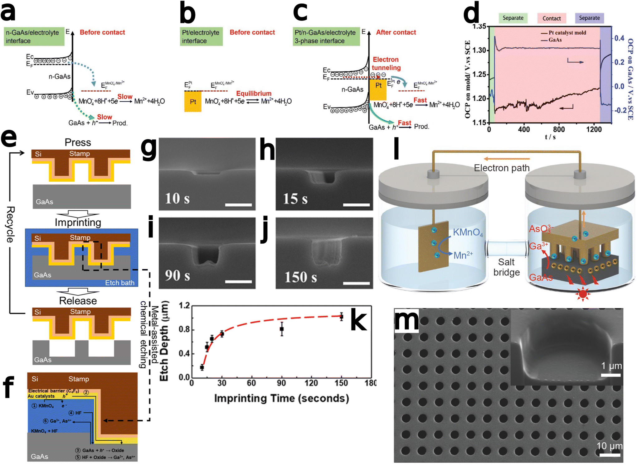 | ||
| Fig. 5 Development of MacImprint for GaAs. (a–d) Theoretical and evidential explanation of the phenomenon driving MacImprint. Interface band diagram for the semiconductor (a) and catalyst (b) prior to imprinting and (c) after imprinting. (d) Electrical potential of the catalyst and semiconductor before, during and after contact. Prior to contact, the Pt catalyst is at a more positive open circuit potential, but once contact is initiated, the high reduction potential of the Pt catalyst drives MacEtch, leading to GaAs oxidation. Oxidation ultimately raises the electrical potential of the GaAs substrate. Initial electrical balance is restored when the mold is removed from the semiconductor. Reproduced from ref. 75 with permission from Royal Society of Chemistry, copyright 2017. (e and f) Detailed schematic of MacImprint (e) showing imprint process and (f) more detailed view including proposed chemical mechanisms and depiction of solution access. (g–k) Imprinting depth with increases in GaAs printing time. Reproduced from ref. 77 with permission from American Chemical Society, copyright 2019. (l) Physical separation of MacImprint into oxidant and etchant and (m) SEM images of etch features following MacImprint. Reproduced from ref. 79 with permission from Springer Nature, copyright 2022. | ||
Zhang et al.76 fabricated curved and arbitrary structures in n-type GaAs with a reusable Pt mold and the MacImprint process. A polymethylmethacrylate (PMMA) imprint mold coated with 100 nm Pt was used in a solution containing H2SO4 and KMnO4. Depths of 600 nm were achieved after 20 min etch times. The imprinted structures were within 95% tolerance of the original mold. Contact pressure was optimized at 0.5 atm, with 0.1 atm not generating an imprint etch, and above 1 atm causing mold deformation and resulting aberration of the etched structures. XPS identified Ga2O3, elemental As and As oxides at the interface between mold and substrate. KMnO4 concentration above 40 mM precluded structure formation. High temperatures disrupted pattern transfer due to oxidant precipitation and excessive bubble generation.
Kim et al.77 utilized the MacImprint approach involving a reusable nanoimprint stamp coated in gold being impressed onto the surface of n-type 〈100〉 GaAs wafers prior to immersion in a permanganate and HF MacEtch solution (Fig. 5e–k). The stamp was coated conformally with the Au catalyst, leading to a greater etch dimension on the wafer surface than on the stamp pattern as the stamp deforms and expands during contact. The increase in etch dimension could be addressed by using Au cap over the pillar in place of the conformal Au film. Additionally, the high aspect ratio of the nanoimprint stamp improved solution access into the etching zone by providing a larger reserve of solution at the catalyst interface when compared to a lower aspect ratio stamp. With the high aspect ratio stamp (i.e., 4.5) the authors were able to fabricate 2.9 aspect ratio trenches, and found the lateral etch rate was increased due to the conformality of the etch structure. Solution access was the limiting factor on the etch rate, suggesting a charge diffusion limited state in the general case only becoming mass transport limited when solution is denied access to the active etch front.
Zhang et al.78 tuned the contact area of a Pt mold for MacImprint to investigate the effect of critical feature dimensions on solution access at the catalyst/semiconductor interface. Both structure size and contact pressure were shown to exert an influence over the final profile. Since the PMMA mold deforms before the rigid semiconductor, the contact area of the mold was shown to increase as more force is applied. With greater contact area, solution access and mass transport at the interface becomes more restricted, so etching was found to initiate at the edge region, where solution access is greater, and gradually proceed to the center of the etched feature. For some feature sizes tested, this effect preceded a protrusion in the center of the etch feature, a phenomenon shown to be dependent on critical mold dimension. Etch depths of 480 and 1330 nm were obtained for features sizes of 3.7 and 56 μm, respectively. Submicron features were etched to a depth of 23 nm. In FEM simulations to determine the source of the nonuniformity, the surface coverage of the GaAs relative to the oxidated species was found to rapidly increase with scaling to smaller feature sizes, indicating greater uniformity at small feature sizes.
Xu et al.79 investigated the localization of the MacEtch reaction by testing the effect of physical separation of the two half-cell reactions into separate cathode and anode reactors (Fig. 5l–m). A Pt plate was submerged in a cathodic solution containing only KMnO4 and electrically contacted to the Pt imprint mold which was placed into direct contact with a n-GaAs substrate in a separate anodic solution containing only the H2SO4 etchant. Reduction at the Pt plate in the cathodic solution consumes electrons from the Pt catalyst, which injects holes into the etched substrate in the anodic solution. As the reproduction dimensions depend on the ratio of mass transport to carrier diffusion, diffusion limited systems more accurately reproduce the parent mold than mass transport limited systems where etching occurs further away from the catalyst. Separating the two half-cells improved etch rate and reproduction accuracy due to the more uniform rate of GaAs dissolution in the absence of off-catalyst hole injection by aqueous MnO4−. Nearly three times depth enhancement (0.67 to 1.63 μm) was observed as result of spatial separation. Additionally, the effect of photo-enhancement on GaAs MacEtch was tested and etch depth was further increased to 2.59 μm under Xe lamp illumination. Contact pressure studies indicated etch rate and final depth increase with increasing contact pressure; however, deformation of the mold under high pressures leads to unpredictable distortion in the final etch profile.
Sun et al.80 investigated the spatially-separated MacImprint method confining not only the oxidant but the catalyst to the cathodic chamber. Using a contact to a glassy carbon mold, hole injection was achieved into the substrate separately confined in acid etchant, while reduction occurred at the Pt catalyst submerged in KMnO4 solution. 1.82 μm depth was reached after 20 minutes of MacImprint. Etch depth was shown to increase with increasing contact pressure, and the glassy carbon mold was shown to tolerate greater pressures than those seen with other MacImprint studies.78,79
In general, MacEtch of GaAs is an adaptable process, with demonstrations of both forward and, albeit more limited, inverse etch progressions. Utilization of a MnO4− oxidant, generally with a less reactive (i.e., less exothermic) etchant such as HF as opposed to H2SO4, improved the micromachining capabilities of MacEtch processing. There is considerable discrepancy concerning the best catalyst, however, with different studies suggesting Au, Pt/Pd, and Pt to be optimal. Crystallographic dependence of the etch was also found to vary with catalyst and etch recipe. The final issue of note concerns the mechanism of oxidation, with differing Raman results suggesting a range of mechanisms. According to Raman spectroscopy analysis presented by Cowley et al.,62 the formation of an arsenic oxide layer preceded etching. The formation of the intermediate arsenic oxide, however, is not universally observed,74 possibly due to differences in MacEtch or other experimental conditions.
GaN
Gallium nitride (GaN) is a wide-bandgap (3.4 eV) binary semiconductor alloy possessing comparable or better electrical characteristics by comparison to similar materials.88–90 Acceptable carrier mobility (1500 cm2 V−1 s−1) and physical properties including a high breakdown voltage (Ecrit = 3.3 MV cm−1), thermal conductivity (1.3 W cm−1 °CE), and operational temperature range (melting point 2500 °C) make GaN broadly useable in optoelectronic and electronic materials.49 GaN has found applications in various fields, including power electronics,91 RF/microwave devices,92 optoelectronics,60 LEDs,93 laser diodes,94 and sensors.95 The blue emissions generated by GaN light emitting diodes have allowed for energy-efficient and inexpensive consumer white lighting.96 Furthermore, GaN nanowires have numerous applications due to their quantum confinement properties and luminescence capabilities.94 MacEtch of GaN structures can improve the fabrication of GaN devices by providing a low-cost and highly adaptable mechanism for surface etching. GaN MacEtch differs from other MacEtch processes by being comparatively delocalized. Despite proceeding largely via an inverse mechanism, etching occurs at micrometer distances from the catalyst and underneath the catalyst as well. Published GaN MacEtch results are provided in Table 2.| Ref. | Temp. | Illumination | Dop. | Cat Mat'l | Cat Thick (nm) | Ox | Etch. | Surf. | Vol ratio | Ox (M) | Etch (M) | Molar ratio | Etch depth (μm) | Features generated |
|---|---|---|---|---|---|---|---|---|---|---|---|---|---|---|
| Key: Ref. – reference number, Temp. – temperature, RT – room temperature, Dop. – doping type, Cat. – catalyst, Mat'l – material, Th. – thickness, UID – unintentionally doped, Ox. – oxidant, Etch. – etchant, Surf. – surfactant, EtOH – ethanol, MeOH – methanol, Vol. – volume, PGaN – porous GaN, NW – nanowire, HAR – high aspect ratio. | ||||||||||||||
| 97 | 500 W Hg arc lamp at <310 nm or <365 nm | n-type | Pt | ∼200 | K2S2O8 | KOH | 0.12 | 0.08 | 0.67 | 1 | Micropillars, squares | |||
| 98 | < 360 nm, 30 mW cm−2 | n-type | Pt | 3–8 | H2O2 (30%) | HF (49%) | EtOH | 1:1:1 |
1 | PGaN | ||||
| 34 | <360 nm, 320 mW cm−2 | UID/n-type | Pt | 7 | H2O2 (30%) | HF (49%) | MeOH | 1:2:1 |
1.5 | PGaN | ||||
| 99 | 100 W Hg lamp | n-type | Pt | 5 | H2O2 (30%) | HF (49%) | MeOH | 2:2:1 |
1 | PGaN | ||||
| 100 | dark | n-type | Pt | H2O | Plane surface | |||||||||
| 101 | 300 K | 130 mW Hg lamp | n-type | AgNO3 | AgNO3 | HF | H2O | NWs | ||||||
| AgNO3 | HF | MeOH | NWs | |||||||||||
| 102 | UV lamp | n-type | Pt | H2O2 (30%) | HF (49%) | MeOH | 7 | NWs | ||||||
| 103 | 100 W Hg lamp | n-type | Pt | 8 | H2O2 (30%) | HF (49%) | MeOH | 2:2:1 |
0.5 | PGaN | ||||
| 38 | 300 K | 90 mW | n-type | Pt | 7–8 | H2O2 (30%) | HF (49%) | MeOH | 2:2:1 |
PGaN | ||||
| 130 mW | >6 | 20 nm NWs | ||||||||||||
| 90 mW | n-type | Au | 7- | H2O2 (30%) | HF (49%) | MeOH | 2:2:1 |
PGaN | ||||||
| 90 mW | n-type | Ir | 7–8 | H2O2 (30%) | HF (49%) | MeOH | 2:2:1 |
honeycomb PGaN | ||||||
| 130 mW | 20 nm NWs | |||||||||||||
| 90 mW | p-type | shallow PGaN | ||||||||||||
| 90 mW | UID | PGaN | ||||||||||||
| 90 mW | n-type | Ag | 7–8 | H2O2 (30%) | HF (49%) | MeOH | 2:2:1 |
PGaN | ||||||
| 130 mW | 3 | H2O2 (30%) | HF (49%) | MeOH | 2:2:1 |
PGaN | ||||||||
| 130 mW | 20 | H2O2 (30%) | HF (49%) | MeOH | 2:2:1 |
PGaN | ||||||||
| 130 mW | n-type | Pt/Au | 7/3 | H2O2 (30%) | HF (49%) | MeOH | 2:2:1 |
PGaN | ||||||
| 130 mW | n-type | Pt/Ag | 7/3 | H2O2 (30%) | HF (49%) | MeOH | 2:2:1 |
PGaN | ||||||
| 104 | RT | Hg lamp UV | UID | Pt/Au | 10/5 | H2O2 (30%) | HF (49%) | μms | HAR NW arrays | |||||
| AgNO3 | AgNO3 | HF | MeOH | 0.3 | HAR NW arrays | |||||||||
| 105 | 300 W Xe Lamp | n-type | Au | ∼25 | K2S2O8 | KOH | 0.1 | 1 | 10 | 0.79 | PGaN | |||
| n-type | Pt | ∼25 | K2S2O8 | KOH | 0.1 | 1 | 10 | 0.835 | PGaN | |||||
| 106 | 300 W Xe lamp | n-type | Au | ∼15 | H2O2 | HF | 1 | 4 | 4 | >μms | (0002) NWs | |||
| 107 | RT | 300 mW Hg lamp at 350–400nm | n-type | AgNO3 | NO3 | HF | 0.01 | 5 | 500 | PGaN | ||||
| n-type | CuSO4 | SO4 | HF | 0.01 | 5 | 500 | 1.8 | NWs, PGaN | ||||||
| 108 | 4 W UV lamp at 365 nm | p-type | AgNO3 | NO3 | HF (49%) | H2O | 0.01 | 14 | 1400 | 0.2 | NWs, PGaN | |||
| 109 | 358 K | 26 W cm−2, 300–450 nm at 6.5 cm | n-type | Pt/Ti | 10/5 | K2S2O8 | KOH | Na3PO4 | 1:1:1 |
0.75 | Micropillar array | |||
| K2S2O8 | KOH | Na3PO4 | 1:6:6 |
3 | Micropillar array | |||||||||
| K2S2O8 | KOH | Na3PO4 | 1:12:12 |
4 | Micropillar array | |||||||||
| 110 | 300 mW Hg lamp | n-type | CuSO4 | SO4 | HF | H2O | 0.01 | 5 | 500 | 6 | Micropillars, squares, stripes | |||
| 111 | RT | 8 W, 254 nm at 3 cm | UID | Pt | 10 | K2S2O8 | HF | 0.04 | 14 | 344 | 0.5 | Sub-μm nanoridges | ||
| 82 | RT | 300 W UV illumin. | n-type | AgNO3 | NO3 | HF | 0.01 | 5 | 500 | NWs | ||||
| AgNO3 | NO3 | HF | 0.02 | 5 | 250 | NWs | ||||||||
| CuSO4 | SO4 | HF | 0.01 | 2.5 | 250 | 2.2 | NWs | |||||||
| CuSO4 | SO4 | HF | 0.01 | 5 | 500 | 3 | NWs | |||||||
| CuSO4 | SO4 | HF | 0.01 | 10 | 1000 | NWs | ||||||||
| CuSO4 | SO4 | HF | 0.02 | 5 | 250 | 3 | NWs | |||||||
| CuSO4 | SO4, H2O2 | HF | 01.6 | 2.5 | 250, 4.2 | PGaN | ||||||||
| 112 | RT | 200 W, 200–450 nm | n-type | Ru | 20 | K2S2O8 | HCl | H2O | 780 nm | Mesas | ||||
Bardwell et al.97 investigated the mechanism for photoenhancement in GaN peroxydisulfide/KOH etching via comparison between masked and unmasked regions of a GaN/AlGaN heteorjunction field effect transistor (Fig. 6a) with gold and silicon oxide as masking materials on the GaN surface. The UV illumination generates both holes in the GaN and reactive oxidant radicals in solution, leading to etching of the substrate. During wet-etching, a roughly ten times etch rate enhancement (43 nm min−1) was observed for the Au mask by comparison to the inert SiOx mask, due to catalytic hole injection by the noble metal. Bardwell et al. claimed the etch mechanism to proceed first at the most crystalline regions, followed by grain boundaries and without etching dislocations due to edge-type trapping of electrons at dislocations leading to recombination.97,113 Similarly, etch rate was found to decrease with increasing distance from the catalyst, due to reduced hole concentrations. Surface roughness was found to be tunable as a result of illumination wavelength and intensity, solution composition and agitation, dislocation density in the substrate, and distance from the catalyst. MacEtch of GaN was found to proceed at all UV wavelengths. However, wavelengths below 310 nm resulted in an enhancement of etch rates from ∼30 nm h−1 to ∼270 nm h−1.
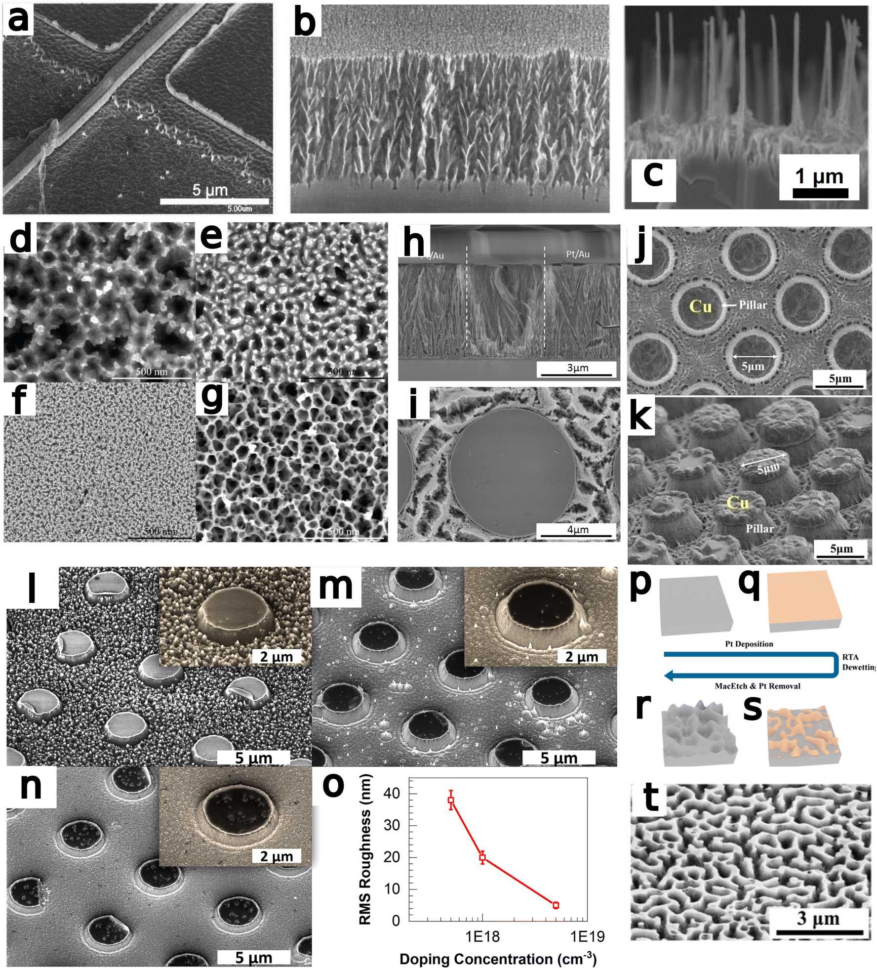 | ||
| Fig. 6 (a) GaN heterostructure FET fabricated by photoenhanced MacEtch of GaN in K2S2O8 solution. Contact pad is shown on the bottom left, gate passing diagonally to the top-right through the source–drain gap. Reproduced from ref. 97 with permission from AIP publishing, copyright 2001. (b) Cross-sectional SEM images at 30° tilt showing porous GaN of a depth of 700 nm and fabricated by MacEtch. Reproduced from ref. 98 with permission from AIP Publishing, copyright 2002. (c) Pt-catalyzed free-standing nanowires fabricated by MacEtch. Reproduced from ref. 102 with permission from IOP Publishing, copyright 2012. (d–g) SEM images of MacEtch samples fabricated with (d) Ag, (e) Au, (f) Pt, and (g) Ir-catalyzed MacEtch. Catalyst material was found to affect both etch rate and pore morphology. Reproduced from ref. 38 with permission from IOP Publishing, copyright 2013. (h and i) SEM images of GaN pillars and nanowires fabricated by MacEtch. Etching and nanowire formation proceeds in off-metal areas. (h) cross sectional image of GaN substrate after etching, (i) plan-view SEM detailing off-metal inverse MacEtch. Reproduced from Ref. 104 with permission from Elsevier, copyright 2016. (j and k) plan and tilt-view SEM images of Cu-assisted MacEtch GaN pillars. Reproduced from ref 110 with permission from MDPI, copyright 2021. (l–o) SEM images of GaN MacEtch samples at (l) 5 × 10¹⁷, (m)1 × 10¹⁸, and (n) 1 × 10¹⁹ dopant concentrations to illustrate the effect of doping on progression of GaN MacEtch. Surface roughness with respect to doping is considered in (o). Reproduced from ref. 109 with permission from AIP Publishing, copyright 2021. (p–s) Process flow to form MacEtch-generated nanoridges and (t) SEM tiltview of post-MacEtch nanoridges. Reproduced from ref. 111 with permission from American Chemical Society, copyright 2023. | ||
Li et al.98 produced porous GaN (Fig. 6b) with Pt-assisted HF/peroxide etching in 1 × 10¹⁸ doped n-GaN substrate. The nanopores demonstrated a greater vertical etch rate than lateral etch rate. In chemiluminescence measurements, a blue-shifted peak was detected at specific etch depths, which was attributed to a band-gap shift resulting from the tapering pillar size. It is suggested quantum confinement at smaller pillar widths is the cause of the blue-shifted emission. Similarly, the blue-shifted emission was found to occur primarily in Pt adjacent areas, where smaller pores evolved than those formed directly under the metal. X-ray diffraction measurements showed a preservation of underlying crystal structure across the etched region. Overall, GaN was found to exhibit a low etch rate, believed to be due to low hole mobility preventing hole diffusion after injection.
Díaz et al.34 generated porous GaN under UV illumination with a HF/CH3OH/H2O2 solution. GaN MacEtch was found to necessitate both UV illumination and a Pt catalyst, due to the barrier to free carrier generation presented by the wide bandgap of GaN and the role of the catalyst in generating oxidative species. Díaz observed a heterogeneous etch result, where a ridge structure forms adjacent to and above the porous substrate and does not exhibit blue-shifted emission. The formation of ridges modulates with etch time, first appearing as disconnected pores, which coalesce to generate broad GaN plateaus, gradually tapering until deep ridges are formed. Both etch progression and ridge formation required a catalyst to proceed, but the porosity and ridge formations were only weakly correlated with proximity to the Pt catalyst. The etch rate was shown to increase with increasing dopant concentration, but the progression from porosity to ridge structure was consistent across all dopant levels tested. Díaz et al. claimed pre-cleaning to remove surface contamination is critical to reproducible etch results. Any contamination adlayer will affect hole injection into the substrate and lead to unpredictable results. Of additional importance is catalyst thickness. A sufficiently thick, discontinuous Pt is critical to etch progression, as continuous films mask the UV illumination and prevent carrier generation.
Duan et al.99 fabricated a hydrogen sensor with porous-GaN (PGaN) fabricated through MacEtch. The induced porosity increased the sensitivity of the device by increasing H absorption. The PGaN was fabricated with solution-based deposition of Pt to prevent adlayer formation on the substrate and eliminate a pre-MacEtch cleaning step. Solution-based catalyst deposition resulted in a different etch progression, as porous material was formed without the generation of ridge and valley superstructures, likely due to decreased catalyst size, increased permeability to the etch solution, and more efficient UV illumination. The depth and diameter of the pores were tuned with etch times to generate nanopores 50–100 nm in diameter and roughly 1 μm depth. The authors observed the deepest pores to begin to dominate the structure as MacEtch times are increased, with eventually all pores being consumed except the deepest. Energy-dispersive X-ray spectroscopy (EDXS) results indicated the presence of the Pt catalyst at the base of the pores.
Murata et al.100 investigated platinum-catalyzed polishing of GaN to achieve atomically smooth surfaces with hole injection in a MacPolishing process (Fig. 7). With a Pt plate and a GaN substrate submerged in water, atomically smooth, planar GaN surfaces were produced. In MacPolished samples, surface damage was reversed via an etch-induced ordering. No illumination is used to effect this process, instead friction between the Pt plate and the GaN wafer provides energy via a tribo-chemical effect. Following flattening for 20 min, a non-uniform atomic step structure developed, giving way to a well-ordered atomically flat step structure after 60 min. Steps were shown to terminate at GaN(0001) faces. Significant PL enhancement was observed following MacPolishing, due to a lack of recombination sites in wafers made surface-defect free due to MacPolishing. Current density measurements indicated friction due to rotation to be necessary for generation of the electrical potential between substrate and catalyst that leads to etching.
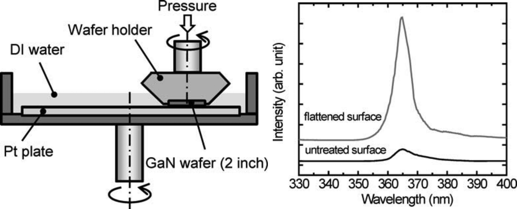 | ||
| Fig. 7 Schema of GaN MacPolishing (left) Observed PL Enhancement following polishing (right). Reproduced from ref. 100 with permission from IOP Publishing, copyright 2012. | ||
Geng et al.101 utilized solution-deposited Ag as a catalyst for MacEtch fabrication of GaN nanowires. As seen previously,99 solution-based etching in a HF/H2O or HF/MeOH solution generated PGaN without long range ridge structures. Porosity was determined by the local presence of the catalyst. The dendritic nature of the Ag deposition caused high static interactions amongst the nanowires, leading them to entwine during etching. Beneath the nanowires, a porous layer developed. After etching the Ag catalyst, the formation of GaN dendrites in the locations formerly hosting Ag dendrites were observed.
Ooi et al.102 fabricated free standing GaN nanowires with a platinum catalyst and a HF, H2O2, and methanol solution under UV illumination (Fig. 6c). Etch progression proceeded from nanopores, to standing nanowires, to collapsed nanowire structures with increasing time. The nanowire formation was observed as spontaneous and a high aspect ratio of 125 in the standing nanowires was measured.
Nie et al.103 generated porous GaN with MacEtch and both Pt and Ag catalysts for biomolecular recognition applications. The etchant solution consisted of HF, H2O2, and methanol. The formation of ridge structures during pore formation was observed, but the authors were able to remove the precipitated ridges via 10 minutes of sonication in methanol. Pore morphology was found to be etch time dependent, as seen in other publications.34,98,99,102
In their 2013 paper, Geng et al.38 evaluated the catalyst effect on GaN MacEtch by comparing etching with Ag, Au, Ir, and Pt under similar conditions. PGaN in n-type, p-type, and UID substrates was fabricated with H2O2, HF, and CH3OH and a range of catalysts (Fig. 6d–g). They observed etch rate to increase with catalyst in the following order: Ag, Au, Ir, and Pt. Geng et al. suggest a mechanism based on work function instead of reduction potential to explain catalyst effect on etch rate and etch progression. It is noted that the work function-dependence of MacEtch rates has been a subject of debate in the field in recent years.28
Wang et al.104 compared the influence of catalyst pattern and dimension over MacEtch-produced GaN nanowires. Catalysts were deposited with either a solution or vacuum based method. In the case of the physical vapor deposition of catalysts, micrometer-scale metal disks or sheets with pore openings were deposited. The MacEtch process was found to be photosensitive and would only proceed under UV illumination, creating a condition where the patterned metal catalyst acted as a photomask for etching, with nanowires developing in off-catalyst areas (Fig. 6h and i). When uniformly-dispersed and solution-deposited Ag was used without patterning a catalyst network, a GaN nanowire field was shown to evolve, terminating at depths more shallow than observed with the patterned catalyst. Photoluminescence emission enhancement in the green range of the visible spectrum was also observed in PGaN samples etched for 10 min. Also generated were GaN nanowires via metal-assisted photochemical etching. Their process parameters included a HF and H2O2 etchant solution and an electrodeposited Au catalyst network. During the etching process, heterogeneous ridge structures were formed as enlarging nanopores coalesced. The UV illumination generated charged holes subsequently consumed by the etchant. The generated electron carriers were reported to migrate through the metal catalyst to reduce peroxide and maintain charge neutrality.
Zhang et al.105 fabricated PGaN with electrodeposited Au and Pt nanoparticles formed in situ on the substrate and carried out hν-MacEtch with peroxydisulfide oxidation in potassium hydroxide. The electrodeposition was performed at a fixed potential determined by cyclic voltammetry to produce optimal catalyst particle size and distribution. The Au particles were on average larger than Pt, and the resulting nanopores reflected the size discrepancy.
Zhang et al.106 fabricated GaN nanowires 8–24 nm in diameter using electrodeposited Au. The high aspect ratio wires were observed to be formed along the (0002) face of wurtzite GaN to a depth of several microns. Nanowire diameter was shown to roughly correspond to nanoparticle size. Electrical potential during deposition was characterized with cyclic voltammetry. Reduction of AuCl4 to form Au(s) was located at −0.5 and −0.9 V.
Wang et al.107 etched GaN in silver or copper nitrate and HF solution in conjunction with UV photo-illumination to produce nanowires. The etching process was dependent on both metal salt and HF concentration, and would not proceed if either species was deficient in solution. Additionally, the behavior of the soluble catalyst species in solution was found to be altered around sites of macroscale substrate defects. For the case of GaN samples grown on 〈111〉 Si, crack structures in the epitaxial layer acted as nucleation sites for the aqueous metal catalyst. As a result, Ag metal dendrites densely precipitated at these structures, creating a self-propagating pattern of unetched GaN due to insufficient UV–generated carriers below the dense metal. A 36 nm min−1 etch rate was measured in off-metal regions.
Kim et al.108 fabricated a multiple quantum well GaN-based LED with surface porosity induced by AgNO3-catalyzed MacEtch. The MacEtched LEDs exhibited red-shifted electroluminescence alongside a 23% increased intensity over non-MacEtched LEDs. This increase was attributed to surface plasmon resonance increasing the internal quantum efficiency of the device.
Chan et al.109 fabricated high aspect ratio micropillar arrays in n-type GaN using a 10 nm Pt catalyst deposited on a 5 nm Ti adhesion layer and a potassium hydroxide, potassium peroxydisulfide, and sodium phosphate etch solution at 85 °C. A dopant dependent etch rate was measured, increasing in etch rate with Si-dopant concentration (Fig. 6l–o). The increased film quality resulting from hydride vapor phase epitaxy was also shown to increase etch rate, due to the improved electronic properties associated with those wafers compared to metalorganic chemical vapor deposition-grown thin films.
Wang et al.110 investigated the formation of high aspect ratio GaN microtrenches using photo-assisted MacEtch with a copper sulfate solution and a Ag/Ni etch mask. The process proceeded with a high vertical etch rate (100 nm min−1) and high vertical/lateral selectivity, attributed to the reduced incidence of UV light on the vertical sidewalls compared to the trenches. Porosity was shown to be dependent on HF acid etchant concentration (Fig. 6j–k). Copper crystalizes preferentially on the Ag/Ni mask, serving as an electron reserve and increasing the local hole concentration, subsequently increasing the rate of hole generation and etching. Microarrays of 1.2 aspect ratio were fabricated, limited by interfacial barriers between doped layers, as the doping was found to greatly affect vertical etch rate and lightly doped material was not etched at a significant rate.
Liao et al.111 investigated MacEtch of UID GaN as an alternative to wet chemical etching to fabricate nanoridge structures with favorable antireflective properties. An evaporated Pt nanomesh was deposited via electron-beam evaporation and the samples exhibited selectivity for vertical over lateral etching. Dewetting control of nanomesh dimensions were shown to influence etch rate and profile. X-ray photoelectron spectroscopy and photoluminescence spectroscopy measurements indicated a surfacial oxide layer on the nanoridges, leading to an n-type doping effect on the MacEtched GaN.
Wang et al.82 studied solution-based, one-step GaN MacEtch under 300 W illumination and made a comparison of etching in CuSO4 and AgNO3 solutions with HF. The Cu etch system exhibited a faster etch rate than Ag, but both terminated etching after 60 minutes regardless of depth. Cu-catalyzed etching was found to produce nanowires instead of nanopores formed during Ag catalyzed MacEtch. This discrepancy was attributed to the formation of Ag dendrites during etching in AgNO3-based solutions. The addition of hydrogen peroxide was found to reduce vertical to lateral etch selectivity as a result of the increased oxidation rate. The authors found that adding H2O2 would prevent the formation of nanowires as nanopolishing dominates and the Cu catalyst is dissolved by the peroxide in solution. A high vertical etch rate (60 nm min−1) and a high selectivity over lateral etching lead to a tapered etch profile after extended etching. The HF concentration was shown to influence the surface roughness of the features, with higher HF concentrations producing a more controlled etch progression and, consequently, a faster etch with smoother sidewalls and better vertical selectivity.
Chan et al.112 studied the feasibility of GaN blue-light emitting diodes defined via Ru-catalyzed MacEtch. Due to the poor selectivity of p-type MacEtch of GaN38 and better electrical and optical characteristics for p-doped topside in optical p–n devices,114 the surficial p-region of the LED was first etched via RIE, and the resulting III-N active and n-doped regions were etched with a MacEtch process utilizing K2S2O8 and HCl. A multi-type heterojunction with varying band gaps and Fermi energies was etched in a one-step process by appropriate selection of catalyst and solution composition under the prevailing MacEtch theory.28 Etch depths of 780 nm were obtained after 18 + 5 min MacEtch, with rates comparable to RIE etch rates. Visible smoothness was evaluated to be roughly equivalent between the two processes; however, MacEtch gave an improved PL response, with a drop of over 60% in PL emission intensity for RIE by comparison to MacEtch. Due to similar surface roughness, the drop in PL emission intensity was attributed to plasma induced crystal damage. A series of devices ranging from 5 to 45 μm in diameter were fabricated. The emission peak was centered at 445 nm and did not show a shift with variation in mesa size. Low leakage current was observed across the device range, with some size dependence. Diode non-idealities were improved over plasma devices, which suffer from parasitic leakage at low voltages. Reduced size negatively impacts EQE at low current densities, attributed to increased series resistance from the diodes and poor contacting. EQE values converged at 13% across most device sizes, with 5 μm devices deviating from this trend to surface roughening.
GaN etching is generally characterized by an exceedingly slow etch rate, due to the high stability of the Ga-face of the GaN crystal structure.115 Stimulation of holes in the valence band following UV-absorption will drive etching at an enhanced rate. The rate of GaN MacEtch, wherein UV illumination generates holes in exposed substrate, is found to depend on the incident photon energy, not only due to increased energy of absorption, but also due to the effects on radical generation in solution.116–118 Illumination below 230 nm was shown to greatly enhance etch rate due to radicalization of etchants in the MacEtch solution.97 Solution composition was found to exert a great influence over the final etch results, with some combinations of oxidant and surfactant generating long-range ridge structures during etching.34,99,103 The utilization of solution-borne catalysts in a one-pot MacEtch configuration was shown to require a sufficient etchant and metal–salt concentration,107 suggesting a complex dynamic between etching and the catalyst solubility. Photoluminescence enhancement and characteristic spectral shifts were observed in the MacEtch-fabricated porous GaN structures, likely due to surface or quantum confinement effects.98,100
InP
Indium phosphide (InP) is a III–V compound semiconductor with a direct bandgap structure and high carrier velocities, making it well-suited to a range of developed and emerging technologies including fiber-optic communication,119 high-speed transistors,120 lasers,94 photonic integrated circuits,58 photodiodes,121,122 and high-frequency electronics.123,124 The high electron mobility and direct bandgap allow for the development of InP optical and electronic devices requiring high frequency switching17 as devices can discharge capacitance at a sufficient rate, improving the RC delay faced by conventional CMOS-based devices.125 To date, the only InP devices fabricated by MacEtch have been produced using an inverse progression MacEtch, due to mass transport limitations of the InP semiconductor leading to hole diffusion and etching in off-catalyst areas. The published InP MacEtch results are presented in Table 3.| Ref. | Temp. | Dop. | Cat Mat'l | Cat. Thick | Illumination | Ox | Etch | Ox (M) | Etch(M) | Molar ratio | Etch Rate (nm min−1) | Etch depth (μm) | Features generated | Feature width |
|---|---|---|---|---|---|---|---|---|---|---|---|---|---|---|
| Key: Ref. – reference number, Temp. – temperature, RT – room temperature, Dop. – doping type, Cat. – catalyst, Mat'l – material, Th. – thickness, Ox. – oxidant, Etch. – etchant, Surf. – surfactant, Vol. – volume | ||||||||||||||
| 127 | 25 °C | n-type | Pt | 30 nm | None | H2O2 | H2SO4 | 2 | 10 | 5 | 10 | 2 | "Frame” | 10 μm |
| 290–390 nm, 2 mW cm−2 | 2 | 10 | 5 | 125 | 7.5 | Micropillar | 30 μm | |||||||
| 2 | 5 | 3 | 120 | 7.2 | Micropillar | 30 μm | ||||||||
| 1 | 15 | 15 | 103 | 6.2 | Micropillar | 30 μm | ||||||||
| 1 | 10 | 10 | 87 | 5.2 | Micropillar | 30 μm | ||||||||
| 1 | 5 | 5 | 57 | 3.4 | Micropillar | 30 μm | ||||||||
| 0.5 | 15 | 30 | 67 | 4 | Micropillar | 30 μm | ||||||||
| 0.5 | 10 | 30 | 53 | 3.2 | Micropillar | 30 μm | ||||||||
| 0.5 | 5 | 10 | 50 | 3 | Micropillar | 30 μm | ||||||||
| Pd | 30 nm | 2 | 10 | 5 | 55 | 3.3 | Micropillar | 30 μm | ||||||
| Au | 30 nm | 2 | 10 | 5 | 38 | 2.3 | Micropillar | 30 μm | ||||||
| 10 | RT | n-type | Au | 30 nm | None | H2O2 | H2SO4 | 24.5 | 20 | 0.61 | Nanopillar | 0.33 μm | ||
| Pt | 30 nm | 24.5 | 10 | 0.29 | Nanopillar | 0.87–1 μm | ||||||||
| Au | 30 nm | 24.5 | 25–28 | 1.3–1.4 | Square | 1–5 μm | ||||||||
| 14 | 17–29 | 0.9–1.5 | Square | 1–5 μm | ||||||||||
| 5.7 | 14–19 | 0.7–1 | Square | 1–5 μm | ||||||||||
| 126 | RT | n-type | Au | 30 nm | None | H2O2 | H2SO4 | 0.7 | Nanofins | 200 nm | ||||
| 17 | RT | n-type | Au | 30 nm | None | H2O2 | H2SO4 | 0.7 | Nanofins | 200 nm | ||||
Asoh et al.127 investigated MacEtch of InP with Pt, Pd, and Au catalysts under ambient light and UV illumination. The MacEtch solution comprised H2SO4 and H2O2. Inverse etching was found to proceed with all three catalysts. However, the etch rate was greatest in the case of the Pt catalyst. Additionally, Pt was the only etchant to initiate etching in the absence of UV light, where an etched frame was generated around the edge of the patterned catalyst. Under UV illumination, etch rates were 10 times higher than under ambient light conditions, due to exciton generation from absorption of UV light by direct-bandgap InP. Microbump arrays of roughly 0.25 aspect ratio were fabricated at an etch rate of 125 nm min−1 (Fig. 8). Without catalysts, no etching was observed, even in the presence of UV illumination. The etch rate was measured as solution composition was varied, and the concentration of the H2O2 oxidant was found to have a greater influence on etch rate than the H2SO4 concentration.
 | ||
| Fig. 8 (a) SEM image of InP microbumps by MacEtch fabricated at regular period of 63 μm and (b) cross-sectional schematic detailing proposed MacEtch mechanism. Reproduced from ref. 127 with permission of IOP Publishing, copyright 2010. | ||
Kim et al.10 carried out an inverse MacEtch process of InP in H2SO4 and H2O2 to fabricate ultra-high aspect ratio nanofins (up to 50:1) while preserving crystallinity and electronic properties. The etched sidewalls were formed with smooth faces defined by the catalyst pattern and composition (Fig. 9a). The verticality of the sidewalls was shown to depend on catalyst material and orientation to InP. For Pt catalysts, vertical sidewalls were formed, but for Au a vertical sidewall was only formed when the catalyst edge was aligned at 45 degrees relative to the (110) primary flat of the InP substrate. In the case of MacEtch of this material, inverse progression was attributed to a 5.4 nm thick insoluble P-based oxide layer at the Au/InP interface, observed via X-ray photoelectron spectroscopy (Fig. 9b and c). The oxidized layer at distant positions relative to the catalyst was measured as ∼1.4 nm. The insoluble oxide layer is suggested to disrupt hole injection at the interface, causing holes to diffuse to off-metal areas to promote etching. By depositing 30 nm thick Au catalyst stripes to delineate the fins, junctionless InP fin field-effect transistors (FinFETs) were fabricated. MacEtch prevented crystal damage to the substrate during etch processing and eliminated challenges associated with deep ion implantation and high temperature annealing steps associated with conventional approaches to transistor fabrication.
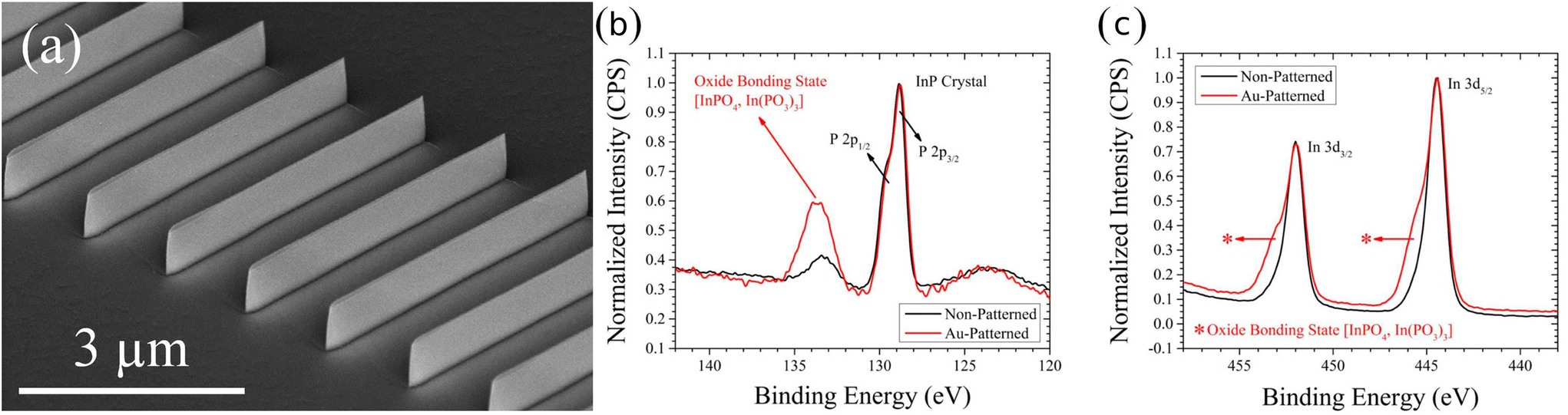 | ||
| Fig. 9 Tilted view SEM image of InP fins fabricated by I-MacEtch (a) and XPS evidence for formation of insoluble POx below catalyst showing oxide bonding states in patterned and off-patterned regions (b and c). Reproduced from ref. 10 with permission from American Chemical Society, copyright 2015. | ||
In Song et al.,17,126 I-MacEtch-fabricated InP FinFET were reported. A 3 × 10⁵ ON/OFF ratio was measured, and a steep subthreshold slope of 63 mV dec−1 indicating sharp turn-on, with the slope decreasing with fin dimension. Fabrication downstream from the etch process required backfilling of MacEtched regions, limiting the critical feature size of subsequent processing steps and leading to increased parasitic resistance arising due to poorly optimized geometry. On-state characteristics include a high drive current (7.2 μA fin−1 or 6 μA μm−1) and a threshold voltage scaling with fin dimension from −4.7 V to −3.5 V (Fig. 10).
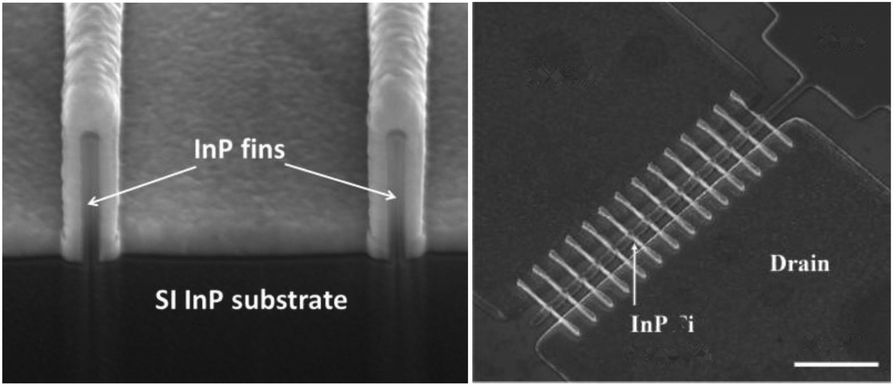 | ||
| Fig. 10 SEM images of MacEtch fabricated 14 nm FinFETs including cross-sectional image detailing channel and gate oxide (left) and tiltview image of FinFET array. Reproduced from ref. 126 (left) and ref. 17 (right) with permission from IEEE, copyright 2015 and 2016. | ||
InP MacEtch, which only proceeds by the inverse mechanism, is both crystallographically dependent and enhanced by UV illumination. The inverse progression generates exceedingly smooth sidewalls, as the dissolution occurs only as a function of proximity to the catalyst. An insoluble oxide layer formed under the catalyst is likely to be a major contributing factor to the exclusive inverse progression of the etch behavior.10
GaP
Gallium phosphide is an indirect bandgap semiconductor with significant use in the fabrication of optoelectronic devices, including photonic crystals,128,129 mechanical resonators,130 photovoltaics,131,132 LEDs,133 and lasers.134 The bandgap of 2.26 eV makes GaP suitable for applications in the visible regions of the electromagnetic spectrum. Furthermore, GaP is closely lattice matched to Si, meaning it can be grown on Si via MOCVD,135 MBE,136 or other epitaxial methods. GaP also has a high electron mobility,49 making it useful in high-speed THz devices137 and power electronics.138Kim et al.139 utilized a 30 nm-thick Pd catalyst and an HF and hydrogen peroxide MacEtch solution to fabricate nano and microscale features in n-type (100) GaP substrate from 200 nm up to several μm in critical feature dimension (Fig. 11.) The MacEtch proceeded in both the forward and inverse progressions, depending on the feature size. Forward progression MacEtch was observed for feature sizes below a critical dimension of 1 μm with Pd catalyst engraved at the bottom of etched regions. A tapered profile in forward etched features was observed due to an only marginal selectivity for vertical over lateral etching. The poor selectivity limited the overall aspect ratio of the etched features to a maximum of 0.45. For larger features, the MacEtch progressed in the inverse, mass transport-limited regime. The inverse MacEtch was found to be anisotropic and generate inverse tapered micro-mesas with elongation in the [110] direction due to a crystallographically-dependent lateral etch progression. It was found that patterned Pd nanomeshes could promote forward and inverse progression MacEtch simultaneously, with GaP nanocones formed on top of micromesas.
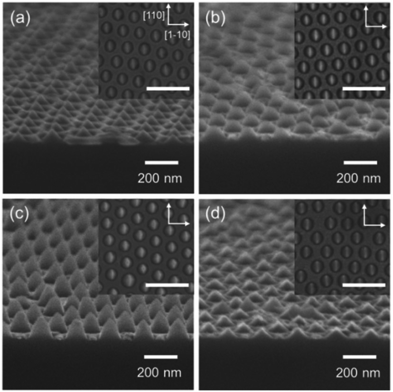 | ||
| Fig. 11 SEM images detailing GaP nanocone etch progression from (a.) 5 minutes, (b.) 7.5 minutes, (c.) 10 minutes, and (d.) 15 minutes of Pd-catalyzed MacEtch. Reproduced from ref. 139 with permission from Royal Society of Chemistry, copyright 2016. | ||
Ternary III–V and III-N semiconductors
The properties of GaAs substrates can be tuned via the introduction of a third substituent into the compound. By introducing a complementary element from the same periodic groups of III and V, material properties, such as lattice constant,140 bandgap energy and momentum (direct or indirect),141 optical emission wavelength,142 chemical reactivity,83 and physical/mechanical properties143,144 can be modified by alloying. While such ternary alloys take on useful physical properties, alloying can complicate fabrication due to the additional constraint of maintaining stoichiometry during processing. III-GaAs semiconductors are generally hindered by the same limitations as those inhibiting GaAs and other binary semiconductor alloys, specifically the lack of controllable, specific etching technologies to achieve desired anisotropicity and solubility. MacEtch does not necessitate high temperature processing and can simplify the process flow to overcome some of the fabrication challenges presented by alloyed GaAs materials. Table 4 collects all published ternary semiconductor MacEtch processing.| Ref. | Material | Temp. | Cat Mat'l | Cat Thick (nm) | Illumin. | Ox | Etch. | Ox. (M) | Etch. (M) | Molar ratio | Prog. | Etch Rate (nm min−1) | Etch depth | Features Generated | Feature width |
|---|---|---|---|---|---|---|---|---|---|---|---|---|---|---|---|
| Key: Ref. – reference number, UID – unintentionally doped Temp. – temperature, RT – room temperature, Cat. – catalyst, Mat'l – material, Th. – thickness, Ox. – oxidant, Etch. – etchant, Prog. – progression, Fwd. – forward, Inv. – inverse, pInGaN – porous InGaN | |||||||||||||||
| 145 | n-In0.53Ga0.47As | RT | Au | 20 | None | KMnO4 | HF | 0.0032 | 14.2 | 0.0002 | Fwd | 62.5 | 500 nm | Nanopillars | 200 nm |
| 0.0053 | 5 | 0.001 | Fwd | 21 | Nanopillars | 200 nm | |||||||||
| 0.0053 | 10 | 0.0005 | Fwd | 23 | Nanopillars | 200 nm | |||||||||
| 0.0053 | 15 | 0.0004 | Fwd | 35 | Nanopillars | 200 nm | |||||||||
| 0.0053 | 20 | 0.0003 | Fwd | 49 | Nanopillars | 200 nm | |||||||||
| 0.0053 | 25 | 0.0002 | Fwd | 19 | Nanopillars | 200 nm | |||||||||
| 0.002 | 14.2 | 0.0001 | Fwd | 12 | Nanopillars | 200 nm | |||||||||
| 0.005 | 14.2 | 0.0004 | Fwd | 38 | Nanopillars | 200 nm | |||||||||
| 0.0053 | 14.2 | 0.0004 | Fwd | 40 | Nanopillars | 200 nm | |||||||||
| 0.01 | 14.2 | 0.0007 | Fwd | 84 | Nanopillars | 200 nm | |||||||||
| 0.015 | 14.2 | 0.0011 | Fwd | 98 | Nanopillars | 200 nm | |||||||||
| 0.02 | 14.2 | 0.0014 | Fwd | 111 | Nanopillars | 200 nm | |||||||||
| n-In0.53Ga0.47As | 5 °C | Au | 20 | None | KMnO4 | HF | 0.0053 | 14.2 | 0.0004 | Fwd | 15 | 145 nm | Nanopillars | 200 nm | |
| n-InAs | RT | Au | 20 | None | KMnO4 | HF | 0.0053 | 14.2 | 0.0004 | Fwd | 16 | Nanopillars | 200 nm | ||
| n-GaAs | 0.0053 | 14.2 | 0.0004 | Fwd | 80 | Nanopillars | 200 nm | ||||||||
| 42 | Al0.55Ga0.45As | 35 | Au | 35 | None | H2O2 | Citric Acid | 17.3 | Inv | 3 | Nanopillars | 1.5 μm | |||
| 50 | Inv | 14 | Nanopillars | 1.5 μm | |||||||||||
| 65 | Inv | 40 | Nanopillars | 1.5 μm | |||||||||||
| Al0.6Ga0.4As | 35 | Inv | 2 | Nanopillars | 1.5 μm | ||||||||||
| 50 | Inv | 12 | Nanopillars | 1.5 μm | |||||||||||
| 65 | Inv | 36 | Nanopillars | 1.5 μm | |||||||||||
| Al0.7Ga0.3As | 35 | Inv | 1 | Nanopillars | 1.5 μm | ||||||||||
| 50 | Inv | 8 | Nanopillars | 1.5 μm | |||||||||||
| 65 | Inv | 28 | Nanopillars | 1.5 μm | |||||||||||
| 146 | In0.2Ga0.8N | Pt | 10 | 700 W UV | H2O2 | HF | 5.08 | 5.64 | 0.9 | Inv | 9.3 | 280 nm | pingan, nanowires | ||
| 147 | UID In0.49Ga0.51P | Au | 35 | None | H2O2 | HF | 6.4 | 14.1 | 0.45 | Inv | 9.7 | 500 nm | Nanomesh | 20 μm | |
| p-In0.49Ga0.51P | Inv | 8.7 | Nanomesh | 20 μm | |||||||||||
| n-In0.49Ga0.51P | Inv | 8.8 | Nanomesh | 20 μm | |||||||||||
InGaAs
Aside from MacEtch, the primary methods of InGaAs processing used to generate vertically-integrated structures include epitaxy and dry etch techniques,148–150 both of which suffer from large process overhead or irreversible lattice damage following processing.145 MacEtch is free from both the aforementioned drawbacks, as it is a benchtop, atmospheric process that derives an anisotropic character from thermodynamic catalysis without either the high energy bombardment of dry etching or the high temperature processing associated with epitaxial growth.Kong et al.145 used Au catalyst in a KMnO4 and HF solution for the forward progression MacEtch of In0.53Ga0.47As to fabricate nanopillars of dimensions between 200 and 300 nm. The pillars exhibited a tapered sidewall profile, due to the formation and slow dissolution of a porous shell adjacent to the etch-field. The vertical etch rate was shown to increase with increasing HF concentration to a climax, then immediately drop off, suggesting that mass transport of solution components to the substrate surface is the limiting factor in etch progression. As a result, increasing the concentration of HF etchant was shown to improve sidewall verticality by increasing etch rate and reducing total lateral etch time. The dropoff in etch rate at high HF concentrations was attributed to the reduction in surfactant concentration. Indeed, increasing the volume of the DI water surfactant improved mass transport in the etch system. At the highest HF concentrations tested, the porous layer was shown to increase in thickness, consuming the entirety of the etched pillars.
As etch progress was found to be constrained in the mass transport domain, the effect of changing oxidant concentrations on etch rate was minimal, due to the increased diffusion of holes away from the etch field, inducing porosity and lateral etching. The hole diffusion was shown to be a result of the reduction in Schottky barrier height of the InGaAs substrate as In concentration is increased (Fig. 12). With a reduced Schottky barrier, holes can diffuse laterally without impetus. The porosity was not completely eliminated by either increasing etchant concentration or reducing oxidant concentration, attributed to the reduced barrier height and ready diffusion of hole carriers. Even for extreme ranges of oxidant conditions, transforming the etch process from the mass transport-limited regime to the charge diffusion-limited regime was not possible due to the rapid hole diffusion, and higher oxidant concentrations led to a thicker porous layer. Additionally, the reduction in barrier height led to InGaAs alloys exhibiting slower etch rates than GaAs, as the increased concentration of holes at the GaAs etchfront can promote faster oxidation and etching. The depth of the porous shell was found to increase with increasing In content. GaAs, by contrast, developed minimal porosity in either the etch field or the pillars.
 | ||
| Fig. 12 (a) Dependence of etch rate on group III stoichiometry, (b and c) cross-sectional SEMs detailing fabricated MacEtch pillars and (d) Schottky barrier diagrams for InGaAs alloys. Reproduced from ref. 145 with permission from American Chemical Society, copyright 2017. | ||
Based on these results, it is suggested that the fabrication of highly-vertical sidewalls with minimal porosity by MacEtch can only be achieved in semiconductor/catalyst systems with significant Schottky barrier height and appropriate selection of etching conditions. To retrospectively mitigate the porosity formed during InGaAs MacEtch, Kong et al. implemented a digital etch process subsequent to the MacEtch step to dissolve the porous oxide. By alternating treatments with UV ozone and HF, porosity on the surface was removed post-MacEtch. Nanoscale MOS-capacitors were fabricated using MacEtch of In0.53Ga0.47As. The MacEtch process, combined with a digital etch procedure, enabled fabricated devices with smooth sidewalls that were free of damages and roughness associated with other forms of etching. Such a sidewall profile led to enhanced device performance evidenced by capacitance-voltage measurements that indicate a low interface state density.
AlGaAs
AlGaAs is unique among semiconductor alloys for retaining a nearly constant lattice constant despite variations in stoichiometric ratio.151 Consequently, alloys of different stoichiometry can be stacked adjacent to each other without having to account for significant lattice mismatch on GaAs substrates. The freedom to vary composition, and consequently other important properties such as optical excitation values, with little cost in terms of lattice strain, makes AlGaAs alloys especially suited for heterogeneous integration152 and optical devices.94AlGaAs is soluble in most common reagents used to dissolve semiconductor-associated oxides, including HF and sulfuric acid.42 AlGaAs is, however, insoluble in a solution of citrate and hydrogen peroxide, but some oxidized states, such as Al2O3, are insoluble in citrate solution and will remain as insoluble deposits. This characteristic of AlGaAs in citrate can be exploited for MacEtch, as the greater rate formation of insoluble oxides under the catalyst than in other areas creates a disparity in solubility. In those zones where soluble oxides form and are then etched by the solution, substrate dissolution can be expected to occur at a faster rate. By producing insoluble oxides at the catalyst interface, the catalyst denies solution access to the AlGaAs, prevents dissolution, and produces an I-MacEtch effect.
Wilhelm et al.42 investigated the inverse MacEtch of AlxGa1−xAs in citric acid and hydrogen peroxide as temperature and stoichiometry (i.e., x) were varied. Increases in temperature were shown to increase both vertical etch rate and lateral etch rate. It is suggested that increasing the temperature accelerates hole diffusion away from the catalyst interface, thereby driving oxidation off-catalyst and increasing the lateral etch rate. As solubility also increases with increased temperature, it can be expected that the rate of dissolution of oxidized AlGaAs will also increase with temperature, leading to increases in both vertical and lateral etch rate. Both the vertical etch rate and vertical/lateral etch selectivity were shown to depend on AlxGa1−xAs stoichiometry (Fig. 13) with the vertical etch rate decreasing as Al content is increased, but at the benefit of improved selectivity for vertical etching over lateral etching. Increasing Al content shifts the valence band edge towards the lower energies of AlAs. As a result, the lower energies of the valence band electrons reduce the thermodynamic drive for hole injection, leading to a lower overall etch rate. Due to the inverse progression, features were fabricated with highly smooth sidewalls as the etch-field is defined by a gradual change in diffusion instead of the catalyst edge pattern.
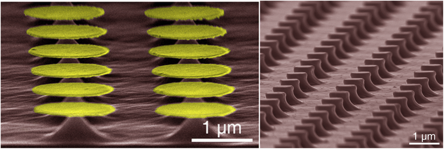 | ||
| Fig. 13 Cross-sectional SEM images of etched nanopillars in Al0.55Ga0.45As (left) and Al0.7Ga0.3As (right). Reproduced from ref. 42 with permission from American Chemical Society, copyright 2018. | ||
InGaN
Ternary GaN alloys find applications in many fields of electronic devices, but they are most noted for their optical properties.153,154 With alloys such as InGaN, the optical emission wavelength can be tuned from the infrared to the ultraviolet ranges of the electromagnetic spectrum encompassing the entire gamut of visible light.155 It is thought the generation of porous structures, via processes like MacEtch, can reduce the lattice strain mismatch between InN and GaN, which so far has limited the applications of InGaN.156After depositing 10 nm Pt catalyst onto the substrate, Najar et al.146 etched InGaN samples with a HF, hydrogen peroxide, and methanol MacEtch solution. Inverse MacEtch proceeded, where the platinum catalyst acted as a photomask for the generation of porous InGaN, giving way to vertical nanowire formation for longer etch times. As etching of the vertical nanowires progressed, the strain generated in the nanowire structure due to the GaN/InN lattice mismatch was compensated by the entwining of nanowires into bundled structures, resulting in a 2 and 4.5 nm red shift in the photoluminescence spectrum of the nanowires. The results suggest that the spontaneously generated nanowires may relieve some of the lattice strain due to mismatch in InGaN samples.
Soopy et al.157 compiled a review of the applications of GaN and In(Ga)N structures fabricated by photo-induced MacEtch. Many structures not fabricated by MacEtch are covered within Soopy,157 but the discussion may be relevant to those interested in MacEtch and associated applications.
InGaP
InGaP is a ternary semiconductor with a tunable bandgap covering the lower energy half of the visible spectrum. Unlike some of the compound ternary semiconductors, InGaP's emission characteristics are tunable with the stoichiometry of the group-III elements, as the bandgap changes from indirect to direct when the In content is increased beyond ∼30%.158 InGaP has seen use in high frequency applications,159 LEDs,160 solar cells161 and bipolar transistors.162,163Wilhelm et al.147 investigated MacEtch of In0.49Ga0.51P with solutions of H2O2 and HF. InGaP was found to undergo inverse MacEtch at a rate below that of other semiconductors. During MacEtch of In0.49Ga0.51P, the vertical etch depth and lateral etch depth were found to increase in off-metal regions only. No etching was found to occur at any position below the catalyst, unlike other etch systems where inverse etching leads to an undercut of the catalyst.42,139 Vertical and lateral etch rates were measured for n-type, p-type, and UID samples. The etch rate was observed to taper off to lower values as etching time increased, due to the etch-induced change in the ratio of substrate surface area to etch solution volume. At extended etch times, a cavity in the In0.49Ga0.51P layer permitted solution access to the deeper underlying GaAs layer driving masked wet-etching of the GaAs along {111} crystal planes. Etching of GaAs proceeded at a faster rate than In0.49Ga0.51P, leading to the generation of an In0.49Ga0.51P nanofoil suspended above a pyramidal void in the GaAs (Fig. 14).
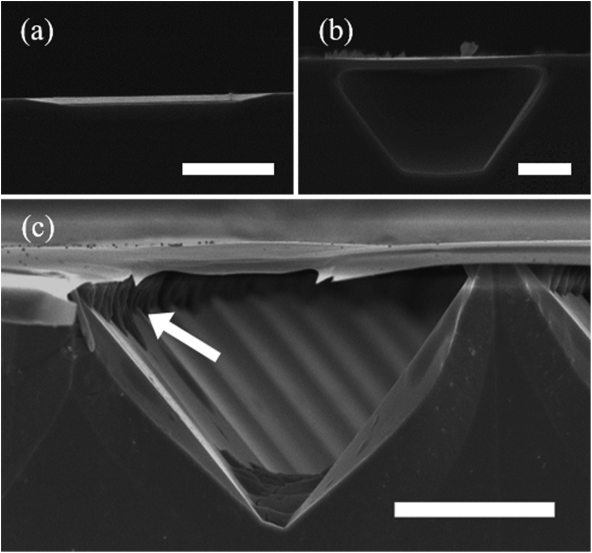 | ||
| Fig. 14 (a–c) Cross-sectional SEM images of InGaP nanofoils fabricated by MacEtch on top of bulk substrates. Reproduced from ref. 147 with permission from American Chemical Society, copyright 2018. | ||
Non III–V semiconductors
MacEtch has been adapted for a handful of additional materials systems that fall outside the realm of both Si and III–V compounds. Materials such as gallium oxide, similar to III–V materials in terms of their desirable optical and electronic properties and process applications, have been investigated by the MacEtch research community. These fields are still emerging, however, and there has been limited characterization of the MacEtch process for many of these materials.Silicon carbide
SiC is an emerging material for optical devices and high power electronics due to its wide bandgap and robust physical characteristics, including high thermal stability, chemical resistance, breakdown field strength, and thermal conductivity.49,164–166 The compound exists in several polytypes, two of the most important forms are the 6H and the 4H phases, which have good stability at applicable temperatures and desirable electronic applications.167 SiC is employed for a range of applications including integrated photonics,168 radiofrequency devices,169 visible LEDs,170 UV photodetectors,171 and sensors.172 Due to the wide bandgap, UV illumination to excite electrons to the conduction band is generally required for MacEtch of SiC to proceed. A table of SiC MacEtch results follows below in Table 5.| Ref. | Mat'l | Illumination | Cat Mat'l | Cat. Thick | Ox. | Etch. | Surf. | Ox. (M) | Etch. (M) | Molar Ratio | Prog | Etch Rate (nm min−1) | Etch Depth | Features Generated | Feature Width |
|---|---|---|---|---|---|---|---|---|---|---|---|---|---|---|---|
| Key: Ref. – reference number, Cat. – catalyst, Mat'l – material, lo. – low doping, hi. – high doping, Th. – thickness, Ox. – oxidant, Etch. – etchant, Surf. – surfactant, Vol. – volume. | |||||||||||||||
| 173 | 6H | 32 mW cm−1, <360 nm | Pt | 10 nm | K2S2O8 | HF | 0.075 | 14 | 0.005 | Inv | Pores | ||||
| 0.15 | 0.5 | 0.300 | Pores | ||||||||||||
| 4H | 0.075 | 14 | 0.005 | Pores | |||||||||||
| 0.15 | 0.5 | 0.300 | Pores | ||||||||||||
| 174 | n-6H | 32 mW cm−2 | Pt | 10 nm | K2S2O8 | HF | 0.1 | 6.3 | 0.016 | Inv | Pores | 150 nm | |||
| 47 | lo. n-4H | 250 W Hg arc | Pt | 0.04 | 1.31 | 0.031 | Inv | ||||||||
| hi. n-4H | Na2S2O8 | HF | 1.3 μm | Pores | |||||||||||
| lo. n-4H | Ann. Pt | ||||||||||||||
| hi. n-4H | 1.11 μm | Pores | |||||||||||||
| p- 4H | 0.78 μm | Pores | |||||||||||||
| 175 | n-type 4H | 18 W UVC | Pt | 300 nm | H2O2 | HF | 0.04 | 1.31 | 0.031 | Inv | Pores | ||||
| 0.15 | 1.31 | 0.115 | Pores | ||||||||||||
| Na2S2O8 | 0.04 | 1.31 | 0.031 | Pores | |||||||||||
| 0.15 | 1.31 | 0.115 | Pores | ||||||||||||
| 176 | n-type 6H | Pt | K2S2O8 | HF | 0.0694 | 28.9 | 0.002 | Inv | 0.56 | 2 μm | Pillars | ||||
| 11 mW cm−2, 254 nm | 0.037 | 28.9 | 0.001 | 0.33 | 408 nm | Pillars | |||||||||
| 27 mW cm−2 | 0.074 | 28.9 | 0.003 | 2.62 | Pillars | ||||||||||
| 177 | n-type 4H | 254 nm | Pt | 15 nm | K2S2O8 | HF | 0.00018 | 0.28 | 0.0006 | Inv | 4 | 120 nm | Holes | 600 nm | |
| 178 | n-type 6H | 13.2 W, 365 nm | Au | H2O2 | HF | H2O | 2 | 5.25 | 0.381 | Inv | 7.7 | Nanovias | 399 nm | ||
| Au/Au | 13.7 | 274 nm | Nanovias | ||||||||||||
| Au/Ag | 8.8 | Nanovias | |||||||||||||
| Au/Pt | 28.5 | Nanowires | |||||||||||||
Rittenhouse et al.173 produced porous 4H and 6H SiC after Pt coating and submersion in a HF and K2S2O8 etching solution (Fig. 15a). UV illumination was filtered to generate 32 mW cm−2 intensity at wavelengths below 360 nm. The concentrations tested were not found to significantly influence the etch outcomes. Short etch times of the 6H polytype yielded ridge structures, while longer etching generated spongy porosity with increased lateral networking of the pores. The overall depth of the porous SiC reached >100 μm below the surface. The 4H polytypes still generated ridges at reduced etch times, but longer etch durations resulted in the formation of nanofingers. MacEtch was found to terminate after, at most, a few hundred nm in the 4H samples, with a high degree of variation from sample to sample. Defects were described to have a highly adverse effect on etch progression. No etch-induced changes in the Raman spectra were observed. The photoluminescence of etched samples was slightly blue-shifted by as much as 20 nm, but no additional PL emissions lines were observed after etching.
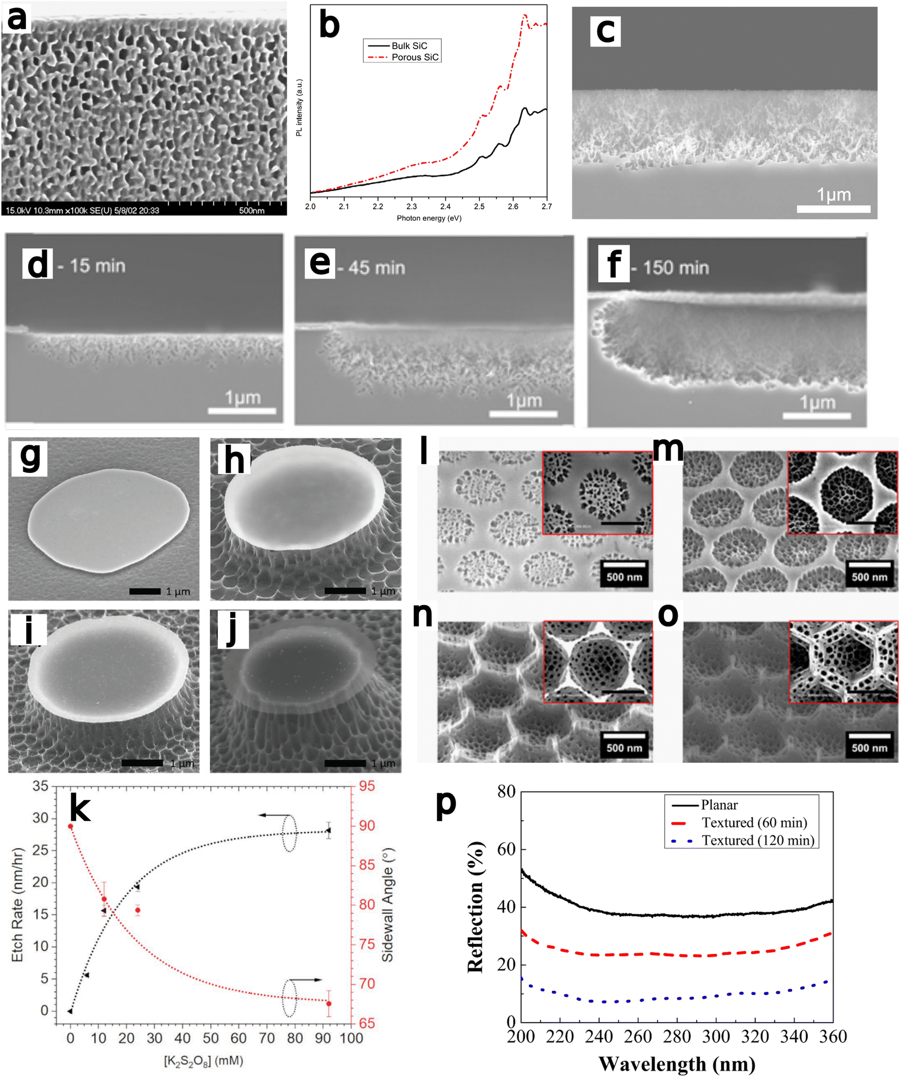 | ||
| Fig. 15 (a) Cross-sectional SEM of a porous 6H SiC fabricated with MacEtch. Reproduced from ref. 173 with permission from Elsevier, copyright 2003. (b) Spectra detailing enhancement of PL intensity after inducing porosity with MacEtch process. Reproduced from ref. 174 with permission from IOP Publishing, copyright 2012. (c) Cross-sectional SEM of induced porosity in 4H SiC after MacEtch. Reproduced from ref. 47 with permission from IOP Science, copyright 2015. (d–f) Three time points (15, 45 and 150 min) indicating progression of p-SiC formation during MacEtch of 4H-SiC. Reproduced from ref. 175 with permission of IOP Science, copyright 2017. (g–j) SEM images demonstrating the influence of oxidant concentration on SiC MacEtch in K2S2O8 solution. [K2S2O8] increased from (g) 6 to (j) 96 mM. (k) Relationship between oxidant concentrations, etch rate and sidewall angle. Reproduced from ref. 176 with permission from John Wiley and Sons, copyright 2021. (l–o) SEM images detailing evolution of SiC holes with increasing MacEtch time. (p) Reduction in reflectance after MacEtch processing for 60 and 120 min. Reproduced from ref. 177 with permission from Elsevier, copyright 2022. | ||
Liu et al.174 fabricated porous SiC with Pt-assisted MacEtch followed with RIE and surface treatments. The authors suggested that dangling bonds generated during MacEtch are reduced following RIE, decreasing overall surface energy and generating deeper pores. The PL intensity was shown to increase following generation of pores in the surface, suggested to arise due to increases in SiC surface area following porosity generation (Fig. 15b).
Leitgeb et al.47 found the progression of porosity formation in 4H SiC MacEtch in Na2S2O8 and HF to depend on the condition of the metal catalyst and substrate doping. Annealing of the Pt catalyst increased pore depth, due to a decrease in the contact resistance between the Pt catalyst and the SiC surface. Lightly doped samples did not generate porous structures, even after annealing, due to the increased electrical resistance of low doped samples reducing the rate of electrical transfer between the two half-cells in the MacEtch Redox reactions. Additional doping with phosphorus lead the lightly doped substrates to generate pores (Fig. 15c).
Leitgeb et al.175 also studied the electrochemical influence of the oxidant and UV intensity on the generation of porosity in 4H SiC. Na2S2O8 and H2O2 were compared in a low volume setup to probe the etching character as the oxidant concentration is naturally depleted, leading to an etch stop. The etch progression was shown to evolve from an initial phase of volatility in the redox potential and etch rates, giving way to a stable etch progression as the oxidant decays (Fig. 15d–f). Eventually the redox potential in the etch solution stabilizes and the total etch depth becomes constant. It was found that as the porosity reached deeper into the substrate, earlier phases of etching would stop developing, and porosity would only be formed at the lower levels. The upper range of the etch region becomes passivated by C–H bonds, preventing further etching. The catalyst was found to act as an anode, despite increases in etch depth with distance from the catalyst. In this work, it was found that Pt was necessary for porosity formation. The authors attribute the progression of etching primarily to the oxidant concentration and the UV light intensity.
Michaels et al.176 investigated the influence of oxidant concentration and UV light intensity on the etch characteristics (Fig. 15g–k). Using K2S2O8 and HF in solution with a Pt catalyst, pillars were formed with varying etch profiles. Carrier generation due to oxidant concentration as well as light energy and intensity were found to govern the etch profile in the fabricated features. Higher energy UV light with greater intensity not only increased the etch rate but also improved sidewall verticality and smoothness. Verticality was found to decrease with increasing oxidant concentration, even as etch rate increased. Raman spectroscopy results indicated an increased presence of a surface oxide following etching. Digital etching with alternating oxide growth and aqueous HF treatment was used to post-process sidewall porosity and reduced overall surface roughness by more than 30%.
Liao et al.177 fabricated holes in 4H SiC using nanosphere lithography and a Pt catalyst (Fig. 15l–p). UV illumination at 254 nm was applied during submersion in a K2S2O8 and HF solution. Inverse etching proceeded, with higher etch rates observed immediately adjacent to the deposited catalyst, indicating rapid consumption of holes due to hole accumulation at the boundary. The degree of metal coverage was found to influence the etch rate. Optical reflectance reduced with increasing etch duration, decreasing by up to 4 times at sub-visible wavelengths measured.
Chen et al.178 fabricated SiC nanovia arrays with MacEtch in a H2O2 and HF solution under UV illumination. A novel aspect of this study included an enhancement of etch rate and feature depth by the application of a catalyst metal to the backside of the wafer. The backside catalyst improves charge distribution in the SiC substrate by providing a sink for space charge accumulation. Nanovias with depths approaching 300 nm were obtained. By changing the backside metal material, the vertical-to-lateral etch rate would also change. The Pt backside catalyst had the fastest vertical etch rate (30 nm min−1), although the lateral etch rate increased to a lesser extent (10 nm min−1). Ag still improved the etch rate (8.8 nm min−1), but less so than Au (17 nm min−1) and Pt.
SiC MacEtch generally follows an inverse etch progression, dependent on UV illumination for the excitation of electrons across the wide bandgap of the material. 4H and 6H polytypes of SiC have been studied as substrates for MacEtch, and generally better results have been obtained in 6H, with deeper pores being formed than in 4H crystals.173 4H SiC MacEtch, on the other hand, was found to depend on dopant concentration and catalyst deposition method, with deeper structures being obtained at high doping concentrations and following catalyst anneal.174
β-Gallium oxide
Gallium oxide is a wide-bandgap material that exists in different crystal phases, with the monoclinic beta-phase being most relevant for device fabrication.180 Beta-phase gallium oxide (β-Ga2O3) is a specific isomorph of gallium oxide where the wide bandgap is a function of the oxygen deficiency and typically in the range of 4.5–5.0 eV. β-Ga2O3 is a semiconductor with unique properties including high thermal stability.181 The wide bandgap, conferring UV transparency and a large breakdown field strength, makes β-Ga2O3 a material of considerable interest for high-power electronics and optoelectronic devices operating in the UV range of the spectrum.182 A summary of β-Ga2O3 MacEtch is included in Table 6.| Ref. | Mat'l | Temp. | Illum | Cat Mat'l | Cat. Thick | Ox. | Etch. | Surf. | Ox. (μM) | Etch. (M) | Molar ratio | Prog. | Etch rate | Etch depth | Feat. | Wid. (μm) |
|---|---|---|---|---|---|---|---|---|---|---|---|---|---|---|---|---|
| Key: Ref. – reference number, Mat'l – material, Temp. – temperature, Illum. – illumination, Cat. – catalyst, Thick. – thickness, Ox. – oxidant, Etch. – etchant, Surf. – surfactant, UID – unintentionally doped, Prog. – progression, Fwd – forward, Inv – inverse, Feat. – feature, Wid. – width | ||||||||||||||||
| 183 | UID 010 | RT | 254 nm | Pt | 15 nm | K2S208 | HF | H20 | 18 | 0.28 | 1556 | Inv | 0.17 | 1 μm | squares | 3 |
| 33 | UID 010 | RT | 254 nm | Pt | 20 nm | K2S2O8 | HF | H20 | 18 | 0.28 | 1556 | Inv | 0.97 | 8 μm | fins | 3 |
Kim et al.183 demonstrated MacEtch of β-Ga2O3 to fabricate metal–semiconductor–metal UV photodiodes, where the MacEtched surface possessed a reduced Schottky barrier height and conferred an increase in gain and responsivity. The devices were fabricated with a ten hour etch of patterned Pt deposited on β-Ga2O3 at room temperature in a HF and K2S2O8 solution under 254 nm UV illumination. The etch process generated crystallographically-aligned nanoscale grooves with a XPS-determined 10% oxygen vacancy. The slow etch rate led to a crystallographic dependence of the etch progression, and also impacted the comparative rate of removal of O and Ga species during etching. As O is removed faster than Ga, the abundance of oxygen vacancies is increased at longer etch times, resulting in oxygen deficiency, a reduction in β-Ga2O3 bandgap, and a lowering of the Schottky-barrier height to the metal. Schottky-barrier heights were determined from the current–voltage (I–V) behavior of the fabricated devices, and the photoresponse of the diodes were measured under 254 nm UV illumination. MacEtch-fabricated diodes showed more efficient light trapping, due to reduced reflectance from the sub-wavelength nanogrooves formed during etching. Dark current in the photodiodes fabricated by MacEtch was found to be significantly increased; however, a greatly enhanced photocurrent ultimately resulted in overall performance enhancement. The reduced Schottky barrier led to a high internal gain, a 2–4 orders of magnitude improvement in responsivity, and three orders of magnitude increase in the normalized photocurrent to dark current ratio (Fig. 16).
 | ||
| Fig. 16 Characterization of textured metal–semiconductor–metal photodiode fabricated by MacEtch and compared with planar photodetectors. Reproduced from ref. 183 with permission from AIP Publishing, copyright 2018. | ||
Huang et al.33 described I-MacEtch of β-Ga2O3 utilizing a Pt catalyst and a MacEtch solution containing HF and K2S2O8. Nanofins with aspect ratios as high as 50 were fabricated using patterned Pt catalysts on a β-Ga2O3 substrate. The progression of nanofin formation was found to be heavily dependent on the orientation of the Pt catalyst, where both verticality and etch rate was shown to vary with the orientation of the Pt lines relative to the [102] direction on a (010) substrate (Fig. 17). The sidewall angles would steepen as the Pt orientation was changed, leading to the generation of pyramidal, trapezoidal, and vertical fins with increasing sidewall angle relative to the [102] direction. The observed changes were stated to arise due to changes in exposed surface compositions. Depending on the direction of etch progression, the concentration of exposed oxygen dangling bonds would change. As O was found to etch faster than Ga, the relative abundance of exposed oxygen atoms will influence the etch character. Similarly, Schottky barrier height was also affected, as surface remodeling during etching altered stoichiometry, reducing the bandgap and consequently the barrier height. MOS capacitors were fabricated with I-MacEtch of β-Ga2O3 and capacitance-voltage (C–V) measurements were made, during which a flat-band voltage shift was found. The change in interface and border trap density responsible for the shift in the voltage response was attributed to the improved surface quality of MacEtched structures by comparison with planar β-Ga2O3.
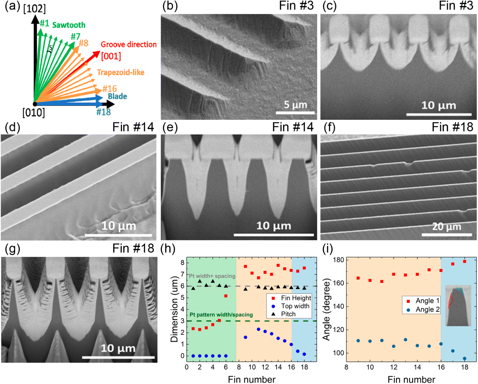 | ||
| Fig. 17 (a) Diagram of etch sidewall morphology as catalyst orientation is varied relative to the substrate. (b–g) Demonstration of variation in nanofin etch progression as Pt catalyst orientation is changed. (h) MacEtched fin dimensions for different catalyst orientations and (i) sidewall angle of etched fins formed under different catalyst orientations. Reproduced from ref. 33 with permission from American Chemical Society, copyright 2019. | ||
β-Ga2O3 MacEtch is highly crystallographically dependent, with both catalyst and substrate crystallinity significantly affecting the etch progression. High performance devices in β-Ga2O3 have been fabricated with MacEtch33,179 and Ren et al. have very recently evaluated the temperature-dependence of β-Ga2O3 finFETs operating up to nearly 300 °C, which were fabricated by an I-MacEtch process. They demonstrated comparable high-temperature performance as planar β-Ga2O3 transistors, determined based on measurements of ON/OFF ratios and subthreshold swing values.184 Huang et al.185 have also compiled a review of β-Ga2O3 etching including a relevant discussion on MacEtch of the material system.
Germanium
Germanium is a group-IV semiconductor with a high intrinsic carrier concentration and electron mobility.49 It is noteworthy particularly for its historical use in the development of semiconductors,186 but Ge is commonly employed in the fabrication of solar cells,187 photodetectors188,189 and other optical components,190 including lasers.191 MacEtch of Ge substrates, which are otherwise easily damaged by many commonly used surface chemistries, may provide a means to take advantage of the attributes of Ge without confronting the issues associated with Ge surface processing. Novel approaches to Ge MacEtch have been adopted by utilizing gentle wet chemistries for catalytic etching (e.g., use of H2O as the primary etchant), or the employment of novel catalysts such as various reduced states of graphene,192,193 which is intriguing as graphene is a promising next generation material for a range of devices.194,195 Ge MacEtch results are tabulated in Table 7.| Ref. | Mat'l | Temp | Cat. Mat'l | Cat. Thick. | Ox. | Etch. | Surf. | Ox. (M) | Etch. (M) | Molar Ratio | Prog. | Etch Rate (nm min−1) | Etch Depth | Features Generated | Feature Width |
|---|---|---|---|---|---|---|---|---|---|---|---|---|---|---|---|
| Key: Ref. – reference number, Mat'l – material, Cat. – catalyst, Th. – thickness, Ox. – oxidant, Etch. – etchant, Surf. – surfactant, Vol. – volume, UID – unintentionally doped, Fwd – forward, Inv – inverse, Red. – reduced, GrOx – graphene oxide. | |||||||||||||||
| 196 | p-type (100) | AgNO3 | |||||||||||||
| 197 | p-type (100) | Ag | 20 nm | O2 | H2O | 5 × 10⁻¹⁰ | 9E-6 | Fwd | 0.07 | 100 nm | Pits | 100 nm | |||
| Pt | 7 nm | 0.03 | 46 nm | Pits | 65 nm | ||||||||||
| Pt/Pd | 5 nm | 70 nm | Impression | 6 mm | |||||||||||
| 198 | p-type (100) | Ag | 20 nm | O2 | H2O | 5 × 10⁻¹⁰ | 9E-6 | Fwd | 0.05 | 6 nm | Pits | ||||
| Pt | 5 nm | 0.03 | 40 nm | Impression | 1 mm | ||||||||||
| 199 | p-type (100) | Ag | 20 nm | O2 | H2O | 5 × 10⁻¹⁰ | 9E-6 | Fwd | Pits | ||||||
| Pt | 7 nm | Pits | |||||||||||||
| 200 | Ag | O2 | H2O | 5 × 10⁻¹⁰ | 9E-6 | Fwd | Pits | ||||||||
| 201 | p-type (100) | 30 °C | Ag | H2O2 | H2O | 2.56 | Fwd | Roughening | |||||||
| 6.4 × 10⁻¹ | roughening | ||||||||||||||
| 1.3 × 10⁻¹ | Pyramids | ||||||||||||||
| 3.2 × 10⁻² | Rough pyramids | ||||||||||||||
| H2O2 | HF | H2O | 8.96 | 5.6 | 1.6 | Texturing | 10 μm | ||||||||
| 6.4 | 11.2 | 0.57 | 5000 | 5 μm | Pits | 10 μm | |||||||||
| 3.84 | 16.8 | 0.23 | Pits | 10 μm | |||||||||||
| 1.28 | 22.4 | 0.06 | Roughening | ||||||||||||
| 0.128 | 24.92 | 0.01 | Roughening | ||||||||||||
| p-type (110) | H2O2 | H2O | 1.3 × 10⁻¹ | Roughening | |||||||||||
| H2O2 | HF | H2O | 6.4 | 11.2 | 0.57 | Pits | |||||||||
| p-type (111) | H2O2 | H2O | 1.3 × 10⁻¹ | Roughening | |||||||||||
| H2O2 | HF | H2O | 6.4 | 11.2 | 0.57 | Pits | |||||||||
| 202 | p-type (100) | Pt | 7 nm | O2 | H2O | Fwd | Pits | ||||||||
| Ag | 20 nm | Pits | |||||||||||||
| Pt cantilever | 0.8 | 4 nm | impression | 1 μm | |||||||||||
| p-type (111) | Pt | 7 nm | pits | ||||||||||||
| Ag | 20 nm | Pits | |||||||||||||
| 203 | 25 °C | AgNO3 | H2O2 | HF | H2O | 7.68 | 11.2 | 0.69 | Fwd | Pores | |||||
| 204 | p-type (100) | Ag | 100 nm | H2O2 | HF | H2O | 0.1 | 5 | Fwd | Pores | |||||
| 0.3 | 5 | Pores | |||||||||||||
| 0.6 | 5 | Pores | |||||||||||||
| AgNO3 | AgNO3 | 1 × 10⁻⁵ | 0.125 | 150 nm | Whiskers | ||||||||||
| 3 × 10⁻⁵ | 0.183 | 220 nm | whiskers | ||||||||||||
| 5 × 10⁻⁵ | 0.233 | 280 nm | Whiskers | ||||||||||||
| 192 | Red. Gr. Oxide | O2 | H2O | 5 × 10⁻¹⁰ | Fwd | 0.02 | 30 nm | Pits | |||||||
| 205 | Red. GrOx. | O2 | H2O | 5 × 10⁻¹⁰ | Fwd | Hollows | |||||||||
| 206 | Red. GrOx. | O2 | H2O | 5 × 10⁻¹⁰ | Fwd | Hollows | |||||||||
| 207 | p-type (100) | 20 °C | Red. GrOx | O2 | H2O | 5 × 10⁻¹⁰ | Fwd | 0.1 | 19.3 nm | Hollows | |||||
| 25 °C | 0.1 | Hollows | |||||||||||||
| 30 °C | 0.1 | Hollows | |||||||||||||
| 35 °C | 0.1 | Hollows | |||||||||||||
| 40 °C | 0.2 | Hollows | |||||||||||||
| 50 °C | 0.3 | Hollows | |||||||||||||
| 60 °C | 0.4 | Hollows | |||||||||||||
| 58 °C | GrOx. | 0.5 | 100 nm | impression | |||||||||||
| 208 | n-type (100) | Ag(NO3) | H2O2 | HF | H2O | 0.50 | 5.53 | 0.09 | Fwd | 770 nm | Nanostructure | 1 μm | |||
| 0.40 | 5.53 | 0.07 | Nanostructure | ||||||||||||
| 0.30 | 5.53 | 0.05 | Nanostructure | ||||||||||||
| 0.20 | 5.53 | 0.04 | Nanostructure | ||||||||||||
| 0.10 | 5.53 | 0.02 | 230 nm | Nanostructure | 160 nm | ||||||||||
| 209 | UID (100) | 40 °C | TiN | 20 nm | KMnO4 | H2O | 0.016 | Inv | 50 | 3 μm | Pit | 6 μm | |||
| 41.7 | 5 μm | V-groove | 10 μm | ||||||||||||
| Ni | 20 nm | 28.9 | 1.3 μm | Pit | |||||||||||
| Ti/Ni | 10 nm/20 nm | 60 | 2.7 μm | Pit | |||||||||||
| Ti | 10 nm | 22.2 | 1.0 μm | Pit | |||||||||||
| 193 | p-type (100) | 34 °C | GrOx. | H2O | Fwd | 8 nm | hollows | ||||||||
| Red. GrOx | 8 nm | Hollows | |||||||||||||
| 210 | p-type (100) | Ag | H2O2 | H2O | Inv | GeOx islands | |||||||||
| 211 | (100) | Au | 40 nm | H2O2 | H2O | 0.61 | Inv | Annulus | 2.4–6 μm with conc. | ||||||
| 0.41 | |||||||||||||||
| 0.31 | |||||||||||||||
| 0.21 | |||||||||||||||
| 0.13 | |||||||||||||||
| 0.08 | |||||||||||||||
| 0.06 | |||||||||||||||
| 0.04 | |||||||||||||||
| 0.03 | |||||||||||||||
Aizawa et al.196 made perhaps the earliest demonstration of Ge MacEtch when local etching was observed in Ge substrates immersed in AgNO3 solutions of concentrations below 0.5 mM. Localized patterns of etching on the Ge surface, described as nano-inukshuks after an Inuit word, were formed after submersion of Ge substrates in AgNO3 solutions (Fig. 18a). TEM results indicated (111)-facing Ag to crystalize on the Ge surface and Ag crystal growth to likely proceed by a Volmer-Weber growth mechanism. Following crystallization, etched nano-inukshuks are formed at concentrations below 0.5 mM Ag+. Ag is deposited on (111) and (100) facets of Ge.
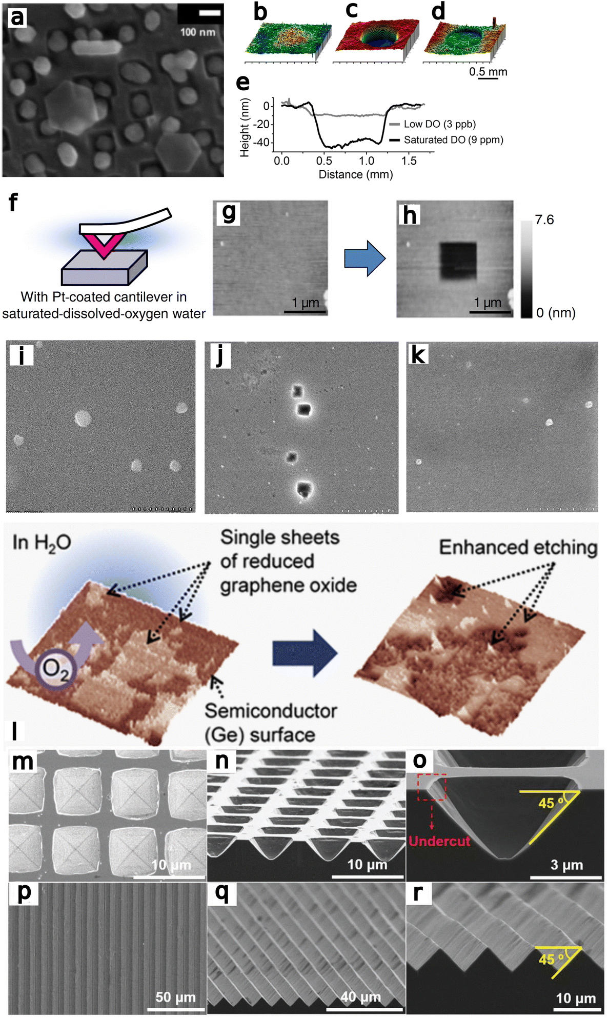 | ||
| Fig. 18 (a) SEM image showing local Ge etching in oxygen-rich water. MacEtch was found to generate nano-inukshuks. Reproduced from ref. 196 with permission from American Chemical Society, copyright 2005. (b–e) Topographic images of MacEtch induced impression recorded with AFM. The impressions were only shown to occur in the presence of high concentrations of dissolved oxygen. Reproduced from ref. 198 with permission from AIP Publishing, copyright 2012. (f–h) Schematic and SEM images demonstrating of AFM-facilitated Ge MacEtch with variation in etch depth dependent on substrate surroundings. The substrate etch proceeds within the boundaries defined by the AFM scan. (f) Depiction of AFM-assisted MacEtch process; (g) depicts the surface prior to AFM-induced etching; (h) depicts the surface following AFM scanning. Reproduced from ref. 199 with permission from Springer Nature, copyright 2013. (i–k) SEM images of etch pits formed by graphene oxide catalyzed Ge MacEtch, (i) Graphene oxide flakes on Ge substrate prior to immersion in water, (j) Ge etch pits formed following submersion in oxygen-rich water, and (k) no etch pits formed in low oxygen water. Reproduced from ref. 192 with permission from IOP Publishing, copyright 2017.192 (l) Schematic depiction of reduced graphene oxide-catalyzed MacEtch of Ge showing catalyst location prior to etching and mass consumption following etching. Reproduced from ref. 205 with permission from Elsevier, copyright 2018. (m–r) SEM images detailing periodic features fabricated by TiN-catalyzed Ge I-MacEtch. Crystallographic etch dependence can be seen in (o and r). Reproduced from ref. 209 with permission from John Wiley and Sons, copyright 2021. | ||
Arima et al.197 induced MacEtch of p- and n-type Ge by deposition of Ag and Pt nanoparticles and immersion in water solutions containing dissolved oxygen. Only under sufficient oxygen concentration (9 ppm) was MacEtch found to proceed. Pyramidal etch pits were generated with crystallographic etching along (111) Ge facets and centered on the catalyst nanoparticles, which were deposited at the base of the pit. When oxygen-free water solutions were implemented, no etch pits were formed. It is indicated that depleted-oxygen water would improve device performance in Ge devices due to a reduction in surface roughening during cleaning. Forward progression MacEtch occurred after a large-scale Pt/Pd pattern was sputter-coated onto Ge, with etching proceeding under the deposited metal pattern.
Kawase et al.198 formed etch pits in (100) Ge with Ag and Pt catalysts. Etching was explained to be mediated by oxidation of Ge and subsequent dissolution in water, as GeO2 is known to be water-soluble. The dissolved oxygen species in the water were described as the oxidant in the MacEtch process. Additionally, a 40 nm depression was induced with a 1 mm diameter deposited Pt film after immersion in O2-rich water solution. AFM scans suggest the shape of the indentations to match the pattern of the deposited metal catalyst (Fig. 18b–e).
Kawase et al.199 developed inverse MacEtch of Ge with Ag and Pt catalysts in oxygen-rich water. Etching was found to proceed along the 〈110〉 direction of the Ge substrate leading to a pyramidal pit topology. The oxidant in the system was again discussed to be dissolved oxygen, which is reduced to form liquid water. To further study the process, Kawase initiated MacEtch of Ge in water with a Pt-coated cantilever in an immersion atomic force microscopy (AFM) system. By manipulating the cantilever, MacEtch of the substrate could be carried out in a controlled fashion with etching proceeding in regions directly contacting the metal-coated cantilever. The etch depth of the pits was found to be dependent on the pressing force with a generally linear increase in etch depth with an increasing pressing force over the range of 1–20 nN pressing force. Dissolved oxygen in the water was found to be necessary for etch progression across the range of pressing forces tested (Fig. 18f–h).
Lee et al.201 investigated surface texturing with Ge MacEtch towards enhanced performance of Ge solar cells. Concentrations of HF, H2O2, and H2O were optimized by their ability to induce a range of surface remodeled features in (100) Ge substrates. Solution variation would generate a range of textures in the Ge surface, including pyramids, octagonal and inverted pyramidal pits, texturing, and induced roughening. Etch rate was found to increase with increasing HF solution, as the etch process shifted towards the oxidation-limited regime. Conversely, the etch rate was stated to be dependent on the peroxide concentration and the rate of Ge oxidation. Solutions containing HF were shown to generate surface roughness at a much accelerated rate; however, the topology of the textured surface was found to be heavily recipe dependent. Additionally, etching was shown to proceed crystallographically, due to reduced bond energies in the {110} and {111} planes and the lower density of the {100} plane. These differences in planar surface orientation led to the preferential formation of {110} and, especially, {111} etch facets. Based on the evaluation of surface texturing during Ge MacEtch under a range of conditions, Ge solar cells were fabricated and their performance was evaluated with respect to reflectance, power conversion efficiency, short circuit current density, open circuit voltage, and fill factor. Considerable performance enhancements were observed in the MacEtch-fabricated devices, particularly in the case of (100) substrates textured in H2O2 and H2O solutions. The discrepancy between increases in light absorption due to MacEtch-induced surface changes and a decrease in overall solar cell efficiency was attributed to a high series resistance diminishing charge collection in solar cells with an otherwise greater rate of light capture.
Kawase et al.200,202 developed a surface flattening process for Ge wafers by utilizing a Pt-coated elastomer pad. Following treatment with the elastomer pad, surface micro-roughness was improved to an average roughness 50% of the pre-treatment value. Also investigated was the nanoscale patterning of Ge wafers utilizing a Pt-coated cantilever immersed in a liquid AFM apparatus.
Rezvani et al.203 fabricated crystallographic pores with a HF, H2O2, and H2O solution and Ge wafers coated with Ag nanoparticles. The MacEtch pores were formed alone on the {111} facets of the Ge substrate. By anodically etching the porous Ge formed by the MacEtch process, Ge nanowires with diameters between 10 and 300 nm and lengths up to 10 μm were generated by an inverse-like etch progression. The nanowires were oriented in the (100) direction, normal to the surface face of the substrate, indicating the crystallographic etching to cease following the application of the applied bias.
Ito et al.204 fabricated Ge nanowhiskers and nanopores with a MacEtch process utilizing AgNO3 and HF/H2O2 solutions. By depositing 100 nm diameter Ag nanoparticles prior to the etch step, porous nanostructures were formed on the surface of Ge wafers. Variation in oxidant concentration was found to exert control over pore size in the nanostructured surfaces. Nanowhiskers were fabricated by etching in a AgNO3 solution, and whisker density and dimensions were shown to depend on AgNO3 concentration.
Nakade et al.192 investigated the use of highly-reduced graphene oxide (hrGO) as a catalyst for the MacEtch of Ge. As metal catalysts can induce surface contamination, it was suggested that a graphene oxide catalyst would allow for surface flattening via a MacEtch process without the presence of metal catalysts. In this work, hrGO was transferred onto Ge wafers, which were then immersed in oxygen-rich water. The graphene oxide induced etching in the presence of the oxygen oxidant (Fig. 18i–k). The graphene was verified to have a dispersed layered structure with thickness of 0.8–1.2 nm, speculated to be due to oxygen sorption onto the monolayer. The graphene oxide flakes were reported to disappear after etching.
Hirano et al.205 advanced the study of graphene oxide-catalyzed MacEtch of Ge (Fig. 18l). Reduced graphene oxide (rGO) sheets were transferred onto a Ge substrate, then immersed in a water bath containing 9 ppm dissolved oxygen. Etching was induced and localized to the area under the rGO sheets, generating shallow pits in the Ge surface. Etch rate was shown to be inversely correlated to the rGO sheet area, with exponential increases in etch rate below 0.5 μm2. The rate increase is attributed to the increased rate of oxidation occurring at the graphene edge. It is suggested that holes in the rGO sheet can increase the etch rate by increasing the rate of oxidation, with the different oxidation potentials between zigzag and armchair edges influencing etch rate, and etching only proceeding at edges or defects in the bulk graphene.
Li et al.206 used in situ AFM to study the local distribution of etch rates during graphene oxide-catalyzed MacEtch of Ge. Their AFM results confirmed a likely dispersion of graphene sheets on the surface. Additional scans conducted separately in water and in air showed a swelling of the graphene oxide sheets when immersed in water. Etching was found to be selective to the region under the graphene sheet, indicating forward etching. The observed MacEtch effect was also preferential along the edge of the graphene by comparison with the central region. The intercalated water layer between the graphene oxide and the Ge was suggested to be crucial for etch progression.
Mikurino et al.207 made a detailed chemical study of the reduction states in reduced graphene oxide during Ge MacEtch in oxygen-rich water by taking XPS measurements of graphene oxidized to varying degrees before and after etching. The mechanism was further probed with ex situ AFM measurements to evaluate the etch rate as the redox potential of the graphene sheets changes. The more reduced states of graphene oxide (i.e., hyd-rGO and amm-rGO) exhibited accelerated etch rates. This observation was suggested to result from the increased availability of oxidative electrons. Additionally, the edge states are discussed to influence etch rate, as carbon atoms at the edge of graphene possess a greater charge density, and “zigzag” edges contain unpaired π-electrons able to reduce dissolved O2 and oxidize the Ge substrate. Due to these charged regions, graphene sheets become oxidized upon immersion in water. The ammonia-reduced graphene oxide was considered the most catalytic. Etch rate variation with temperature was used to make measurements of the activation energy of the etch reaction, and generally increased with temperature. Additionally, etch rate is believed to increase as the etch proceeds due to changes in graphene oxidation. The conclusions drawn from this robust and interesting study provide further evidence for the role of redox potential in MacEtch.
Chen et al.208 investigated light trapping enhancements on n-type Ge substrates following MacEtch. The influence of H2O2 over texture dimensions in HF, H2O2, and H2O MacEtch solutions was studied using a low concentration of AgNO3 as the catalyst. Ge mass consumption was the highest in samples etched in the highest oxidant concentration solutions. Here, etch rate was suggested to be determined by H2O2 concentration. MacEtch was shown to reduce optical reflectance across the visible and near-infrared spectral ranges, and attributed to an increase in light trapping capability of the etched samples. Reflectance was not found to depend on total mass consumption, however, and the greatest absorption was seen with a lower concentration of oxidant, with 97% molar ratio showing a better absorbance profile than 93%, 95%, and 99%. This phenomenon is suggested to arise due to competition between catalytic and non-catalytic etching process, which proceed in tandem.
Liao et al.209 demonstrated TiN and Ni-catalyzed I-MacEtch of Ge (Fig. 18m–r). According to the authors, MacEtch proceeded in the inverse progression due to the strong adhesion of the catalyst layer to the substrate preventing solution access at the interface. Combined with the high hole mobility in Ge, catalyst-patterned samples immersed in KMnO4-based solutions were shown to undergo I-MacEtch. Inverted pyramid and V-groove arrays were fabricated after 1 hour and 2 hours etching durations, respectively. Ni was also shown to drive I-MacEtch, with a bare Ni catalyst delaminating after a short period, but with a Ni catalyst deposited on top of a Ti adhesion layer forming deep inverted pyramids. Schottky barrier heights were extracted from Schottky diode transport measurements using Norde's method to analyze I–V curves. Ge was found to experience a high degree of Fermi level pinning. The Schottky barrier heights for all catalysts were measured similarly. This junction configuration led to upward band bending, and rapid hole injection and diffusion away from the interface, promoting I-MacEtch. XPS results indicated that the TiN catalyst was not degraded during etching. Moreover, reflectivity in the textured samples reduced to less than 10% after TiN MacEtch.
Ogasawara et al.193 used MacEtch of Ge substrates as a means to probe the catalytic activity of nanocarbon sheets. Reduced graphene oxide was compared to graphene oxide in terms of its electrochemical properties as well as the catalytic etching induced when brought into interfacial contact with Ge substrates immersed in water. Hollows were formed at the locations of graphene sheets, with depths surpassing 10 nm. Deeper hollows were formed at locations coated by reduced graphene oxide, indicating a higher catalytic activity. The authors highlighted MacEtch a viable characterization tool to evaluate the oxidative-reductive potential of functionalized graphene sheets or other functional nanocarbon materials.
Dutta et al.210 formed shell-shaped, micron-scale islands of Ge oxide following MacEtch in a dilute H2O2/H2O solution and AgNO3 catalyst. An abundance of oxide deposits were found to increase with Ag catalyst and HF concentration. The islands were randomly distributed across the surface, with roughly a 2:1 stoichiometric ratio. XRD results indicated the islands to be crystalline. The exact mechanism for formation was unclear, as Ge oxides are generally soluble in water solutions. The oxides were found to be in the hexagonal phase. Further, XPS analysis suggested the formation of the GeO2 phase. Optical reflectance was reduced after the catalytic oxide formation process. The bandgap of the resulting oxide, as determined from absorbance measurements, was shown to increase with increasing oxide presence. The I–V characterization results indicated the presence of a GeO2/Ge heterojunction with hole-blocking capabilities. Resistivity was also found to increase with increasing oxide formation.
Lidsky et al.211 investigated the variation in Au-catalyzed MacEtch rate enhancement with oxidant concentration. Rings of Au were fabricated on (100) Ge substrates prior to immersion in etch baths consisting of H2O and H2O2 with concentrations ranging between 0.03 M and 0.61 M. An empirical formula for the etch rate with distance from catalyst was derived from the etch profiles as measured by profilometery. The total etch depth showed direct dependence on the etchant concentration, but etch rate enhancement was found to exhibit a maximum at concentrations between 0.2 M and 0.6 M. The diffusion length of holes in the Ge substrate was approximated as an exponentially decaying trend from empirical fits to the data. The etched substrates were found to maintain their crystallinity and showed no amorphous character. The etch rate and profile is explained to be independent of doping type.
Ge MacEtch is a highly-crystallographic process that follows a forward etch progression, but generates results resembling those of semiconductor systems that progress via an inverse mechanism. Due to the crystallographic nature of Ge MacEtch, the catalyst sinks into the substrate but leaves behind a proceeding crystallographic etch front, generally resulting in inverse pyramidal features. Both metal-salt196,204,208 and oxygen-containing water solutions were shown to drive MacEtch, as were solutions containing only H2O and other oxidants and etchants, including HF and H2O2. In graphene oxide catalyzed studies, solution access was shown to be critical for etch progression. When MacEtch was catalyzed by graphene oxide, etching would proceed only at the edge of the graphene oxide sheets, or underneath them only when pores were opened in the surface of the two-dimensional material.
Conclusions and perspectives
Of the III–V systems investigated for MacEtch, GaAs has been the most developed and the effects of both catalyst and solution composition were investigated along with other application critical parameters, including feature dimensions and catalyst thickness.69 High aspect ratio structures were fabricated74 in GaAs substrates, and characterization of the surface following MacEtch was carried out62,74 while advanced optical devices like LEDs21 and optical transmission gratings22 were demonstrated using MacEtch-fabricated micro- and nano-scale structures. Additionally, the MacImprint technique has been developed to an advanced state80 and applied to GaAs processing. GaN processing has received significant development as well, doubtless in part due to the difficulties associated with GaN wet etching. Restricted to inverse etching regimes due to the requirement for UV light to drive etch progression, GaN MacEtch has produced structures at the microscale and below, including nanowires,111 micropillars,107 and porous GaN.105 In the limited research into InP MacEtch so far, evidence was presented to elucidate the mechanism behind the inverse progression that has been shown to generate extremely-smooth sidewalls and high aspect ratio features. Using this inverse etch method, high performing FinFETs were fabricated with 14 nm widths and near-ideal subthreshold slope, demonstrating that MacEtch can be used to generate structures with competitive technical performance. Nanocones in GaP substrates were fabricated under both forward and inverse progression MacEtch regimes. The MacEtch process has also been applied to ternary III–V alloys, and in general progression was shown to depend on material stoichiometry as an additional parameter. SiC has been MacEtched under UV illumination to generate nanoholes, nanopillars, and various degrees of porosity in 4H and 6H SiC polymorphs. Nanofins and nanosquares have been fabricated in β-Ga2O3, and a variety of subtractive features, including pits, roughening, and surface indentations have been formed in Ge substrates using MacEtch.MacEtch and its derivative approaches for micro- and nano-fabrication take advantage of the specific electronic configuration of a semiconductor to metal junction to selectively etch either interfacial regions or off-metal regions depending on a multitude of factors described in this Review. The need for broadly applicable and adaptable etch processes for III–V semiconductors and other materials has stimulated research in the field. Novel approaches to adapting MacEtch to a wider range of materials have been developed, including changes to solution composition, catalyst makeup, and external conditions like photo-illumination. The reductive potential of the catalyst as an intermediate between the semiconductor valence band edge and oxidant reduction potential is a critical factor to drive hole-injection into the semiconductor and enable catalytic oxidation.
For MacEtch of III–V semiconductors and other materials, innovative approaches to etching have been developed and will continue to evolve. Beyond expanding to etching next-generation materials, including other III–V alloys, ferroelectrics, perovskites, van der Waals materials, and two-dimensional monolayer systems, MacEtch needs to address shortcomings in the current process flow. Specifically needing to be addressed are issues relating to the implementation and scaling of the MacEtch process, including affordable and CMOS-compatible catalysts, issues around repeatability and uniformity, controllability of etched feature dimensions, and comprehensive evaluation of etch progression in heterojunction systems, both axial and lateral. Additionally, the exact chemical reactions governing MacEtch are not clearly elucidated, despite viable proposals (Table 8) to explain the observed phenomena. Advances in in situ analysis to more precisely determine reaction species would certainly benefit the MacEtch community. The recent development of two-dimensional materials,193,205,207,213 oxides,25 and nitrides209,214 as catalysts, one-pot MacEtch,66,82 and MacImprint36,215 techniques are promising developments on these issues. By the same token, the advantages of MacEtch have the potential to greatly innovate mainstay nanofabrication techniques, by improving processing throughput, reducing fabrication complexity, avoiding surface damage, and lowering costs.
| Material | Proposed reactions | Ref. |
|---|---|---|
| GaAs | GaAs(s) + MnO4−(aq) + H+(aq) → Ga3+(aq) + Asn+(aq) + Mn2+(aq) + H2O(l) | 63 |
 (1) (1) |
69 | |
| Ga2O3(s) + 3H2SO4(l) → Ga2(SO4)3(aq) + 3H2O (2) | ||
| GaAs(s) + 6H+(aq) → Ga3+(aq) + As3+(aq) | 62 | |
| GaAs(s) + 3H2O2(l) + 3HF(l) → GaF3(s) + H3AsO3(l) + 3H2O(l) (1) | 73 | |
| GaAs(s) + 4H2O2(l) + 3HF(l) → GaF3(s) + H3AsO3(l) + 4H2O(l) (2) | ||
| MnO4−(aq) + 8H+(aq) + 5e− → Mn2+(aq) + 4H2O(l) (1) | 75 | |
| GaAs(s) + 3H2O(l) → Ga3+(aq) + AsO33−(aq) + 6H+(aq) + 6e− (2) | ||
| MnO4−(aq) + 8H+(aq) + 5e− → Mn2+(aq) + 4H2O(l) (1) | 76 | |
| GaAs(s) + 3H2O(l) + 6h+ → Ga3+(aq) + AsO33−(aq) + 6H+(aq)(2) | ||
| MnO4−(aq) + 8H+(aq) + 5e− → Mn2+(aq) + 4H2O(l) (1) | 78 | |
| GaAs(s) + 6H2O(l) + 6h+ → H3GaO3·H3GaO3(aq) + 6H+(aq) (2) | ||
| H3GaO3 · H3AsO3(aq) + αGaAs(s) → αGaAs · ½ (Ga2O3 · As2O3)(aq) + 3H2O(l) (3) | ||
| GaN | GaN(s) + γ → GaN(s) + e− + p+ (1) | 97 |
| GaN(s) + 3p+ → Ga3+ + ½N2 (2) | ||
| S2O8(aq) + 2e− → SO42−(aq) (3) | ||
| S2O8(aq) + γ → 2SO42−(aq) (4) | ||
| 2GaN(s) + 3H2O2(l) + 4HF(l) → 2GaF2(s) + 4H2O(l) + N2(g) | 38 | |
|
101 | |
|
105 | |
| GaN(s) + 2H2O(l) → Ga2O3(s) + N2(g) + 6H+(aq) + 6e− (1) | 107 | |
| Ga2O3(s) + xHF(l) → GaFx(3−x)(s) + H2O(l) (2) | ||
| 2GaN(s) + 6h+→2Ga3+(aq) + N2(g) (1) | 106 | |
| Ga3+(aq) + xHF(l) → GaFx(3−x)(s) + xH+(aq) (2) | ||
| SiC | 4S2O82−(aq) + SiC(s) + 2H2O(l) + 6HF(l) → 8SO42−(aq) + 8H+(aq) + CO2(g) + H2SiF6(s) | 173,174 |
| 4S2O82−(aq) + 8e− → 8SO42−(aq) (1) | 47, 175 and 176 | |
| SiC(s) + 4H2O(l) + 8h+ → SiO2(s) + 8H+(aq) + CO2(g) (2) | ||
| SiO2(s) + 6HF(l) → H2SiF6(s) + 2H2O(l) (3) | ||
| SiC(s) + 4H2O(l) + 8h+ → SiO2(s) + 8H+(aq) + CO2(g) | 178 | |
| β-Ga2O3 |
|
179 |
| Ge | O2(g) + 4H+(aq) + 4e− → 2H2O(l) (1) | 197, 198 and 205 |
| Ge(s) + 2H2O(l) → GeO2(s) + 4H+(aq) + 4e− (2) | ||
| H2O2(l) + e− → 2H2O(l) + 2h+ (1) | ||
| Ge(s) + 2H2O2(l) → GeO2(s) + 2H2O(l) (2) | ||
| GeO2(s) + H2O(l) → H2GeO3(l) (3) | 210 | |
| H2O2(l) + e− → 2H2O(l) + 2h+(1) | ||
| Ge(s) + 2H2O2(l) → GeO2(s) + 2H2O(l) (2) | ||
| GeO2(s) + 4HF(l) → GeF4(s) + 2H2O(l) (3) | ||
| GeO2(s) + 6HF(l) → H2GeF6(aq) + 2H2O(l) (4) | 201 | |
| Ge(s) + O2(aq) → GeO2(s) (1) | 206 | |
| GeO2(s) + H2O(l) → H2GeO3(aq) (2) | ||
| 3Ge(s) + xh+ + 6OH2− → 3GeO2−(s) + (4 − x)e− + 3H2O(l) | 212 |
Conflicts of interest
There are no conflicts to declare.Acknowledgements
Figures were created with Google Collab216 and assembled in Inkscape.217 The authors are grateful to Dr. Ivan Puchades and Mr. Samuel Boyd for fruitful discussions. This material is based upon work supported by the National Science Foundation under Award No. 2235443 and by the Micron Foundation through the Micron Underrepresented Student Fellowship.References
- X. Li, Metal Assisted Chemical Etching for High Aspect Ratio Nanostructures: A Review of Characteristics and Applications in Photovoltaics, Curr. Opin. Solid State Mater. Sci., 2012, 16(2), 71–81, DOI:10.1016/j.cossms.2011.11.002.
- H.-D. Um, N. Kim, K. Lee, I. Hwang, J. Hoon Seo, Y. J. Yu, P. Duane, M. Wober and K. Seo, Versatile Control of Metal-Assisted Chemical Etching for Vertical Silicon Microwire Arrays and Their Photovoltaic Applications, Sci. Rep., 2015, 5(1), 11277, DOI:10.1038/srep11277.
- V. P. Sharma, R. Shukla, C. Mukherjee, P. Tiwari and A. K. Sinha, Study of Metal-Assisted Chemical Etching of Silicon as an Alternative to Dry Etching for the Development of Vertical Comb-Drives, J. Micromanuf., 2023, 6(1), 19–26, DOI:10.1177/25165984211033422.
- B. P. Azeredo, J. Sadhu, J. Ma, K. Jacobs, J. Kim, K. Lee, J. H. Eraker, X. Li, S. Sinha, N. Fang, P. Ferreira and K. Hsu, Silicon Nanowires with Controlled Sidewall Profile and Roughness Fabricated by Thin-Film Dewetting and Metal-Assisted Chemical Etching, Nanotechnology, 2013, 24(22), 225305, DOI:10.1088/0957-4484/24/22/225305.
- H.-J. Syu, S.-C. Shiu, Y.-J. Hung, C.-C. Hsueh, T.-C. Lin, T. Subramani, S.-L. Lee and C.-F. Lin, Influences of Silicon Nanowire Morphology on Its Electro-Optical Properties and Applications for Hybrid Solar Cells: Si Nanowire Morphology, Electro-Optical Properties and Hybrid Solar Cells, Prog. Photovolt. Res. Appl., 2013, 21(6), 1400–1410, DOI:10.1002/pip.2375.
- H. Asoh, A. Uehara and S. Ono, Nanopatterning of Si Substrate Using Nanospheres as a Mask for Localized Anodization, Jpn. J. Appl. Phys., 2004, 43, 5667, DOI:10.1143/JJAP.43.5667.
- K.-Q. Peng, Y.-J. Yan, S.-P. Gao and J. Zhu, Synthesis of Large-Area Silicon Nanowire Arrays via Self-Assembling Nanoelectrochemistry, Adv. Mater., 2002, 14(16), 1164–1167, DOI:10.1002/1521-4095(20020816)14:16<1164::AID-ADMA1164>3.0.CO;2-E.
- W. Chern, K. Hsu, I. S. Chun, B. P. d. Azeredo, N. Ahmed, K.-H. Kim, J. Zuo, N. Fang, P. Ferreira and X. Li, Nonlithographic Patterning and Metal-Assisted Chemical Etching for Manufacturing of Tunable Light-Emitting Silicon Nanowire Arrays, Nano Lett., 2010, 10(5), 1582–1588, DOI:10.1021/nl903841a.
- F. J. Wendisch, M. Rey, N. Vogel and G. R. Bourret, Large-Scale Synthesis of Highly Uniform Silicon Nanowire Arrays Using Metal-Assisted Chemical Etching, Chem. Mater., 2020, 32(21), 9425–9434, DOI:10.1021/acs.chemmater.0c03593.
- S. H. Kim, P. K. Mohseni, Y. Song, T. Ishihara and X. Li, Inverse Metal-Assisted Chemical Etching Produces Smooth High Aspect Ratio InP Nanostructures, Nano Lett., 2015, 15(1), 641–648, DOI:10.1021/nl504136c.
- B. Ki, Y. Song, K. Choi, J. H. Yum and J. Oh, Chemical Imprinting of Crystalline Silicon with Catalytic Metal Stamp in Etch Bath, ACS Nano, 2018, 12(1), 609–616, DOI:10.1021/acsnano.7b07480.
- L. Romano, M. Kagias, J. Vila-Comamala, K. Jefimovs, L.-T. Tseng, A. V. Guzenko and M. Stampanoni, Metal Assisted Chemical Etching of Silicon in the Gas Phase: A Nanofabrication Platform for X-Ray Optics, Nanoscale Horiz., 2020, 5(5), 869–879, 10.1039/C9NH00709A.
- T. K. Kim, J.-H. Bae, J. Kim, M. K. Cho, Y.-C. Kim, S. Jin and D. Chun, Curved Structure of Si by Improving Etching Direction Controllability in Magnetically Guided Metal-Assisted Chemical Etching, Micromachines, 2020, 11(8), 744, DOI:10.3390/mi11080744.
- H. Hu, P. K. Mohseni, L. Pan, X. Li, S. Somnath, J. R. Felts, M. A. Shannon and W. P. King, Fabrication of Arbitrarily Shaped Silicon and Silicon Oxide Nanostructures Using Tip-Based Nanofabrication, J. Vac. Sci. Technol., B: Nanotechnol. Microelectron.: Mater., Process., Meas., Phenom., 2013, 31(6), 06FJ01, DOI:10.1116/1.4831767.
- K. Balasundaram, P. K. Mohseni, Y.-C. Shuai, D. Zhao, W. Zhou and X. Li, Photonic Crystal Membrane Reflectors by Magnetic Field-Guided Metal-Assisted Chemical Etching, Appl. Phys. Lett., 2013, 103(21), 214103, DOI:10.1063/1.4831657.
- L. Romano and M. Stampanoni, Microfabrication of X-Ray Optics by Metal Assisted Chemical Etching: A Review, Micromachines, 2020, 11(6), 589, DOI:10.3390/mi11060589.
- Y. Song, P. K. Mohseni, S. H. Kim, J. C. Shin, T. Ishihara, I. Adesida and X. Li, Ultra-High Aspect Ratio InP Junctionless FinFETs by a Novel Wet Etching Method, IEEE Electron Device Lett., 2016, 37(8), 970–973, DOI:10.1109/LED.2016.2577046.
- D. M. Pera, I. Costa, F. Serra, G. Gaspar, K. Lobato, J. M. Serra and J. A. Silva, Development of a Metal-Assisted Chemical Etching Method to Improve Light-Capture in Monocrystalline Silicon Solar Cells, Sol. Energy Mater. Sol. Cells, 2023, 251, 112143, DOI:10.1016/j.solmat.2022.112143.
- C. Lima Anderson, W. Nemeth, H. L. Guthrey, C.-S. Jiang, M. R. Page, S. Agarwal and P. Stradins, Nanopinhole Passivating Contact Si Solar Cells Fabricated with Metal-Assisted Chemical Etching, Adv. Energy Mater., 2023, 13(11), 2203579, DOI:10.1002/aenm.202203579.
- Z. Xu, H. Zhang, C. Chen, G. Aziz, J. Zhang, X. Zhang, J. Deng, T. Zhai and X. Zhang, A Silicon-Based Quantum Dot Random Laser, RSC Adv., 2019, 9(49), 28642–28647, 10.1039/C9RA04650J.
- P. K. Mohseni, S. Hyun Kim, X. Zhao, K. Balasundaram, J. Dong Kim, L. Pan, J. A. Rogers, J. J. Coleman and X. Li, GaAs Pillar Array-Based Light Emitting Diodes Fabricated by Metal-Assisted Chemical Etching, J. Appl. Phys., 2013, 114(6), 064909, DOI:10.1063/1.4817424.
- R. Liu, X. Zhao, C. Roberts, L. Yu, P. K. Mohseni, X. Li, V. Podolskiy and D. Wasserman, Enhanced Optical Transmission through MacEtch-Fabricated Buried Metal Gratings, Adv. Mater., 2016, 28(7), 1441–1448, DOI:10.1002/adma.201505111.
- W. McSweeney, H. Geaney, C. Glynn, D. McNulty and C. O'Dwyer, Pseudocapacitive Charge Storage at Nanoscale Silicon Electrodes, ECS Trans., 2015, 66(6), 39, DOI:10.1149/06606.0039ecst.
- R. F. Balderas-Valadez, V. Agarwal and C. Pacholski, Fabrication of Porous Silicon-Based Optical Sensors Using Metal-Assisted Chemical Etching, RSC Adv., 2016, 6(26), 21430–21434, 10.1039/C5RA26816H.
- A. Mallavarapu, P. Ajay, C. Barrera and S. V. Sreenivasan, Ruthenium-Assisted Chemical Etching of Silicon: Enabling CMOS-Compatible 3D Semiconductor Device Nanofabrication, ACS Appl. Mater. Interfaces, 2021, 13(1), 1169–1177, DOI:10.1021/acsami.0c17011.
- N. Geyer, B. Fuhrmann, Z. Huang, J. De Boor, H. S. Leipner and P. Werner, Model for the Mass Transport during Metal-Assisted Chemical Etching with Contiguous Metal Films As Catalysts, J. Phys. Chem. C, 2012, 116(24), 13446–13451, DOI:10.1021/jp3034227.
- Z. Huang, N. Geyer, P. Werner, J. de Boor and U. Gösele, Metal-Assisted Chemical Etching of Silicon: A Review: In Memory of Prof. Ulrich Gösele, Adv. Mater., 2011, 23(2), 285–308, DOI:10.1002/adma.201001784.
- L. Kong, B. Dasgupta, Y. Ren, P. K. Mohseni, M. Hong, X. Li, W. K. Chim and S. Y. Chiam, Evidences for Redox Reaction Driven Charge Transfer and Mass Transport in Metal-Assisted Chemical Etching of Silicon, Sci. Rep., 2016, 6(1), 36582, DOI:10.1038/srep36582.
- H. Han, Z. Huang and W. Lee, Metal-Assisted Chemical Etching of Silicon and Nanotechnology Applications, Nano Today, 2014, 9(3), 271–304, DOI:10.1016/j.nantod.2014.04.013.
- S. J. Pearton, J. C. Zolper, R. J. Shul and F. Ren, GaN: Processing, Defects, and Devices, J. Appl. Phys., 1999, 86(1), 1–78, DOI:10.1063/1.371145.
- S. Guo, D. Yang, D. Wang, X. Fang, D. Fang, X. Chu, X. Yang, J. Tang, L. Liao and Z. Wei, Response Improvement of GaAs Two-Dimensional Non-Layered Sheet Photodetector through Sulfur Passivation and Plasma Treatment, Vacuum, 2022, 197, 110792, DOI:10.1016/j.vacuum.2021.110792.
- L. Zamora-Peredo, L. García-González, J. Hernández-Torres, I. E. Cortes-Mestizo, V. H. Méndez-García and M. López-López, Photoreflectance and Raman Study of Surface Electric States on AlGaAs/GaAs Heterostructures, J. Spectrosc., 2016, 2016, e4601249, DOI:10.1155/2016/4601249.
- H.-C. Huang, M. Kim, X. Zhan, K. Chabak, J. D. Kim, A. Kvit, D. Liu, Z. Ma, J.-M. Zuo and X. Li, High Aspect Ratio β-Ga2O3 Fin Arrays with Low-Interface Charge Density by Inverse Metal-Assisted Chemical Etching, ACS Nano, 2019, 13(8), 8784–8792, DOI:10.1021/acsnano.9b01709.
- D. J. Díaz, T. L. Williamson, I. Adesida, P. W. Bohn and R. J. Molnar, Morphology Evolution and Luminescence Properties of Porous GaN Generated via Pt-Assisted Electroless Etching of Hydride Vapor Phase Epitaxy GaN on Sapphire, J. Appl. Phys., 2003, 94(12), 7526–7534, DOI:10.1063/1.1628833.
- J. D. Kim, M. Kim, L. Kong, P. K. Mohseni, S. Ranganathan, J. Pachamuthu, W. K. Chim, S. Y. Chiam, J. J. Coleman and X. Li, Self-Anchored Catalyst Interface Enables Ordered Via Array Formation from Submicrometer to Millimeter Scale for Polycrystalline and Single-Crystalline Silicon, ACS Appl. Mater. Interfaces, 2018, 10(10), 9116–9122, DOI:10.1021/acsami.7b17708.
- A. Sharstniou, S. Niauzorau, A. Junghare and B. P. Azeredo, Metal-Assisted Electrochemical Nanoimprinting of Porous and Solid Silicon Wafers, J. Visualized Exp., 2022,(180), e61040, DOI:10.3791/61040.
- Y. Chen, C. Zhang, L. Li, S. Zhou, X. Chen, J. Gao, N. Zhao and C.-P. Wong, Hybrid Anodic and Metal-Assisted Chemical Etching Method Enabling Fabrication of Silicon Carbide Nanowires, Small, 2019, 15(7), 1803898, DOI:10.1002/smll.201803898.
- X. Geng, B. K. Duan, D. A. Grismer, L. Zhao and P. W. Bohn, Catalyst and Processing Effects on Metal-Assisted Chemical Etching for the Production of Highly Porous GaN, Semicond. Sci. Technol., 2013, 28(6), 065001, DOI:10.1088/0268-1242/28/6/065001.
- D. R. Turner, On the Mechanism of Chemically Etching Germanium and Silicon, J. Electrochem. Soc., 1960, 107(10), 810, DOI:10.1149/1.2427519.
- E. S. Kooij, K. Butter and J. J. Kelly, Silicon Etching in HNO 3/HF Solution: Charge Balance for the Oxidation Reaction, Electrochem. Solid-State Lett., 1999, 2(4), 178, DOI:10.1149/1.1390775.
- J. E. A. M. van den Meerakker, The Reduction of Hydrogen Peroxide at Silicon in Weak Alkaline Solutions, Electrochim. Acta, 1990, 35(8), 1267–1272, DOI:10.1016/0013-4686(90)90060-D.
- T. S. Wilhelm, Z. Wang, M. A. Baboli, J. Yan, S. F. Preble and P. K. Mohseni, Ordered AlxGa1−xAs Nanopillar Arrays via Inverse Metal-Assisted Chemical Etching, ACS Appl. Mater. Interfaces, 2018, 10(32), 27488–27497, DOI:10.1021/acsami.8b08228.
- C. Q. Lai, H. Cheng, W. K. Choi and C. V. Thompson, Mechanics of Catalyst Motion during Metal Assisted Chemical Etching of Silicon, J. Phys. Chem. C, 2013, 117(40), 20802–20809, DOI:10.1021/jp407561k.
- R. A. Lai, T. M. Hymel, V. K. Narasimhan and Y. Cui, Schottky Barrier Catalysis Mechanism in Metal-Assisted Chemical Etching of Silicon, ACS Appl. Mater. Interfaces, 2016, 8(14), 8875–8879, DOI:10.1021/acsami.6b01020.
- K. Murata, T. Yorioka, N. Shiraiwa, T. Ito, S. Shingubara and T. Shimizu, Effect of Etching Solution Concentration on Preparation of Si Holes by Metal-Assisted Chemical Etching, Jpn. J. Appl. Phys., 2022, 61(SJ), SJ1007, DOI:10.35848/1347-4065/ac678c.
- Z. Huang, T. Shimizu, S. Senz, Z. Zhang, N. Geyer and U. Gösele, Oxidation Rate Effect on the Direction of Metal-Assisted Chemical and Electrochemical Etching of Silicon, J. Phys. Chem. C, 2010, 114(24), 10683–10690, DOI:10.1021/jp911121q.
- M. Leitgeb, A. Backes, C. Zellner, M. Schneider and U. Schmid, Communication—The Role of the Metal-Semiconductor Junction in Pt-Assisted Photochemical Etching of Silicon Carbide, ECS J. Solid State Sci. Technol., 2016, 5(3), P148–P150, DOI:10.1149/2.0021603jss.
- K. Balasundaram, J. S. Sadhu, J. C. Shin, B. Azeredo, D. Chanda, M. Malik, K. Hsu, J. A. Rogers, P. Ferreira, S. Sinha and X. Li, Porosity Control in Metal-Assisted Chemical Etching of Degenerately Doped Silicon Nanowires, Nanotechnology, 2012, 23(30), 305304, DOI:10.1088/0957-4484/23/30/305304.
- NSM Archive - Physical Properties of Semiconductors. https://www.ioffe.ru/SVA/NSM/Semicond/(accessed 2023-09-29).
- J. S. Blakemore, Semiconducting and Other Major Properties of Gallium Arsenide, J. Appl. Phys., 1982, 53(10), R123–R181, DOI:10.1063/1.331665.
- Full article: Group III-V semiconductors as promising nonlinear integrated photonic platforms. https://www.tandfonline.com/doi/full/10.1080/23746149.2022.2097020 (accessed 2023-09-29).
- V. M. Ustinov and A. E. Zhukov, GaAs-Based Long-Wavelength Lasers, Semicond. Sci. Technol., 2000, 15(8), R41, DOI:10.1088/0268-1242/15/8/201.
- M. Kim and M.-K. Kim, Four-Dimensional Nanofabrication for next-Generation Optical Devices, J. Korean Phys. Soc., 2022, 81(6), 516–524, DOI:10.1007/s40042-022-00409-x.
- Materials | Free Full-Text | Overview of the Current State of Gallium Arsenide-Based Solar Cells. https://www.mdpi.com/1996-1944/14/11/3075 (accessed 2023-09-29).
- M. M. Rahman, A. M. Asiri, T. A. Tabbakh and A. Khan, Inamuddin. Post-Transition Metals; BoD – Books on Demand, 2021 Search PubMed.
- R. R. LaPierre, M. Robson, K. M. Azizur-Rahman and P. Kuyanov, A Review of III–V Nanowire Infrared Photodetectors and Sensors, J. Phys. Appl. Phys., 2017, 50(12), 123001, DOI:10.1088/1361-6463/aa5ab3.
- G. Koblmüller, B. Mayer, T. Stettner, G. Abstreiter and J. J. Finley, GaAs–AlGaAs Core–Shell Nanowire Lasers on Silicon: Invited Review, Semicond. Sci. Technol., 2017, 32(5), 053001, DOI:10.1088/1361-6641/aa5e45.
- S.-H. Hsu, Reflectively Coupled Waveguide Photodetector for High Speed Optical Interconnection, Sensors, 2010, 10(12), 10863–10875, DOI:10.3390/s101210863.
- C. P. Dietrich, A. Fiore, M. G. Thompson, M. Kamp and S. Höfling, GaAs Integrated Quantum Photonics: Towards Compact and Multi-Functional Quantum Photonic Integrated Circuits, Laser Photonics Rev., 2016, 10(6), 870–894, DOI:10.1002/lpor.201500321.
- H. A. A. Abdul Amir, M. A. Fakhri and A. Abdulkhaleq Alwahib, Review of GaN Optical Device Characteristics, Applications, and Optical Analysis Technology, Mater. Today: Proc., 2021, 42, 2815–2821, DOI:10.1016/j.matpr.2020.12.727.
- Y. Yasukawa, H. Asoh and S. Ono, Periodic GaAs Convex and Hole Arrays Produced by Metal-Assisted Chemical Etching, Jpn. J. Appl. Phys., 2010, 49, 6502, DOI:10.1143/JJAP.49.116502.
- A. Cowley, J. A. Steele, D. Byrne, R. K. Vijayaraghavan and P. J. McNally, Fabrication and Characterisation of GaAs Nanopillars Using Nanosphere Lithography and Metal Assisted Chemical Etching, RSC Adv., 2016, 6(36), 30468–30473, 10.1039/C5RA23621E.
- M. DeJarld, J. C. Shin, W. Chern, D. Chanda, K. Balasundaram, J. A. Rogers and X. Li, Formation of High Aspect Ratio GaAs Nanostructures with Metal-Assisted Chemical Etching, Nano Lett., 2011, 11(12), 5259–5263, DOI:10.1021/nl202708d.
- Y. Yasukawa, H. Asoh and S. Ono, GaAs Microarrays by Noble-Metal Assisted Chemical Etching, ECS Trans., 2008, 16(3), 253, DOI:10.1149/1.2982563.
- Y. Yasukawa, H. Asoh and S. Ono, Site-Selective Chemical Etching of GaAs through a Combination of Self-Organized Spheres and Silver Particles as Etching Catalyst, Electrochem. Commun., 2008, 10(5), 757–760, DOI:10.1016/j.elecom.2008.02.024.
- Y. Yasukawa, H. Asoh and S. Ono, Site-Selective Metal Patterning/Metal-Assisted Chemical Etching on GaAs Substrate through Colloidal Crystal Templating, ECS Trans., 2008, 13(3), 83, DOI:10.1149/1.2913083.
- Y. Yasukawa, H. Asoh and S. Ono, Ordered Hole Arrays on GaAs Fabricated by Metal-Assisted Chemical Etching, ECS Meet. Abstr., 2009, MA2009-01(21), 879, DOI:10.1149/MA2009-01/21/879.
- Y. Yasukawa, H. Asoh and S. Ono, Morphological Control of Periodic GaAs Hole Arrays by Simple Au-Mediated Wet Etching, J. Electrochem. Soc., 2012, 159(5), D328, DOI:10.1149/2.021206jes.
- H.-Y. Cheung, H. Lin, F. Xiu, F. Wang, S. Yip, J. C. Ho and C.-Y. Wong, Mechanistic Characteristics of Metal-Assisted Chemical Etching in GaAs, J. Phys. Chem. C, 2014, 118(13), 6903–6908, DOI:10.1021/jp500968p.
- Y. Song and J. Oh, Thermally Driven Metal-Assisted Chemical Etching of GaAs with in-Position and out-of-Position Catalyst, J. Mater. Chem. A, 2014, 2(48), 20481–20485, 10.1039/C4TA05095A.
- H. Asoh, Y. Suzuki and S. Ono, Metal-Assisted Chemical Etching of GaAs Using Au Catalyst Deposited on the Backside of a Substrate, Electrochim. Acta, 2015, 183, 8–14, DOI:10.1016/j.electacta.2015.05.167.
- H. Asoh, R. Imai and H. Hashimoto, Au-Capped GaAs Nanopillar Arrays Fabricated by Metal-Assisted Chemical Etching, Nanoscale Res. Lett., 2017, 12(1), 444, DOI:10.1186/s11671-017-2219-1.
- P. Lova, V. Robbiano, F. Cacialli, D. Comoretto and C. Soci, Black GaAs by Metal-Assisted Chemical Etching, ACS Appl. Mater. Interfaces, 2018, 10(39), 33434–33440, DOI:10.1021/acsami.8b10370.
- T. S. Wilhelm, A. P. Kolberg, M. A. Baboli, A. Abrand, K. A. Bertness and P. K. Mohseni, Communication—Black GaAs with Sub-Wavelength Nanostructures Fabricated via Lithography-Free Metal-Assisted Chemical Etching, ECS J. Solid State Sci. Technol., 2019, 8(6), Q134, DOI:10.1149/2.0311906jss.
- J. Zhang, L. Zhang, W. Wang, L. Han, J.-C. Jia, Z.-W. Tian, Z.-Q. Tian and D. Zhan, Contact Electrification Induced Interfacial Reactions and Direct Electrochemical Nanoimprint Lithography in N-Type Gallium Arsenate Wafer, Chem. Sci., 2017, 8(3), 2407–2412, 10.1039/C6SC04091H.
- J. Zhang, L. Zhang, L. Han, Z.-W. Tian, Z.-Q. Tian and D. Zhan, Electrochemical Nanoimprint Lithography: When Nanoimprint Lithography Meets Metal Assisted Chemical Etching, Nanoscale, 2017, 9(22), 7476–7482, 10.1039/C7NR01777D.
- K. Kim, B. Ki, K. Choi, S. Lee and J. Oh, Resist-Free Direct Stamp Imprinting of GaAs via Metal-Assisted Chemical Etching, ACS Appl. Mater. Interfaces, 2019, 11(14), 13574–13580, DOI:10.1021/acsami.9b00456.
- J. Zhang, J. Guo, D. Chen, M. M. Sartin, L. Zhang, Z.-Q. Tian and D. Zhan, Interfacial Reactions and Mass Transport in the Processes of Electrochemical Nanoimprint Lithography, J. Phys. Chem. C, 2019, 123(44), 27073–27079, DOI:10.1021/acs.jpcc.9b08468.
- H. Xu, L. Han, J.-J. Su, Z.-Q. Tian and D. Zhan, Spatially-Separated and Photo-Enhanced Semiconductor Corrosion Processes for High-Efficient and Contamination-Free Electrochemical Nanoimprint Lithography, Sci. China: Chem., 2022, 65(4), 810–820, DOI:10.1007/s11426-021-1194-3.
- W. Sun, H. Xu, L. Han, C. Wang, Z. Ye, J.-J. Su, Y.-F. Wu, S. Luo and D. Zhan, CMOS-Compatible Electrochemical Nanoimprint:High Throughput Fabrication of Ordered Microstructures on Semiconductor Wafer by Using a Glassy Carbon Mold, Electrochim. Acta, 2023, 142700, DOI:10.1016/j.electacta.2023.142700.
- S.-D. Wang, S.-Y. Chen, S.-P. Hsu, C.-Y. Liao and W.-Y. Hsu, Ag and Cu Metal-Assisted Chemical Etching for Diamond-Wire-Sawn Single-Crystalline Silicon Solar Cell, Appl. Surf. Sci., 2022, 578, 152050, DOI:10.1016/j.apsusc.2021.152050.
- Q. Wang, W. Yang, S. Gao, W. Chen, X. Tang, H. Zhang, B. Liu, G. Han and Y. Huang, GaN Nanowires Prepared by Cu-Assisted Photoelectron-Chemical Etching, Nanoscale Adv., 2023, 5(8), 2238–2243, 10.1039/D2NA00889K.
- W. P. Gomes, Chapter 6 - Wet Etching of III–V Semiconductors, In Handbook of Advanced Electronic and Photonic Materials and Devices, ed. H. Singh Nalwa, Academic Press, Burlington, 2001, pp. 221–256. DOI:10.1016/B978-012513745-4/50018-4.
- P. Schmuki, J. Fraser, C. M. Vitus, M. J. Graham and H. S. Isaacs, Initiation and Formation of Porous GaAs, J. Electrochem. Soc., 1996, 143(10), 3316, DOI:10.1149/1.1837204.
- D. Tromans, G. G. Liu and F. Weinberg, The Pitting Corrosion of P-Type GaAs Single Crystals, Corros. Sci., 1993, 35(1), 117–125, DOI:10.1016/0010-938X(93)90141-3.
- S. L. Cheng, C. H. Chung and H. C. Lee, A Study of the Synthesis, Characterization, and Kinetics of Vertical Silicon Nanowire Arrays on (001)Si Substrates, J. Electrochem. Soc., 2008, 155(11), D711, DOI:10.1149/1.2977548.
- S. Ono, S. Kotaka and H. Asoh, Fabrication and Structure Modulation of High-Aspect-Ratio Porous GaAs through Anisotropic Chemical Etching, Anodic Etching, and Anodic Oxidation, Electrochim. Acta, 2013, 110, 393–401, DOI:10.1016/j.electacta.2013.06.025.
- E. F. Schubert, Room temperature properties of Si, Ge, GaAs, and GaN. Room temperature properties of Si, Ge, GaAs, and GaN. https://sites.ecse.rpi.edu/~schubert/Course-reference-materials/Materials-Semiconductors-Si-Ge-GaAs-&-GaN.pdf (accessed 2023-06-16).
- T. Hashizume, S. Ootomo, S. Oyama, M. Konishi and H. Hasegawa, Chemistry and Electrical Properties of Surfaces of GaN and GaN/AlGaN Heterostructures, J. Vac. Sci. Technol., B: Microelectron. Nanometer Struct.–Process., Meas., Phenom., 2001, 19(4), 1675–1681, DOI:10.1116/1.1383078.
- F. A. Ponce and D. P. Bour, Nitride-Based Semiconductors for Blue and Green Light-Emitting Devices, Nature, 1997, 386(6623), 351–359, DOI:10.1038/386351a0.
- T. J. Flack, B. N. Pushpakaran and S. B. Bayne, GaN Technology for Power Electronic Applications: A Review, J. Electron. Mater., 2016, 45(6), 2673–2682, DOI:10.1007/s11664-016-4435-3.
- U. K. Mishra, L. Shen, T. E. Kazior and Y.-F. Wu, GaN-Based RF Power Devices and Amplifiers, Proc. IEEE, 2008, 96(2), 287–305, DOI:10.1109/JPROC.2007.911060.
- B. Melanson, M. Seitz and J. Zhang, Inverse Tapered AlGaN Micropillar and Nanowire LEDs for Improved Light Extraction Efficiency at 270 Nm, IEEE Photonics J., 2022, 14(6), 1–10, DOI:10.1109/JPHOT.2022.3221353.
- E. Odoh and N. Augustine Shuye, A Review of Semiconductor Quantum Well Devices. 2015 Search PubMed.
- K. T. Upadhyay and M. K. Chattopadhyay, Sensor Applications Based on AlGaN/GaN Heterostructures, Mater. Sci. Eng., B, 2021, 263, 114849, DOI:10.1016/j.mseb.2020.114849.
- Energy Savings Forecast of Solid-State Lighting in General Illumination Applications, 2019. https://www.energy.gov/sites/prod/files/2019/12/f69/<?pdb_no 2019?>2019<?pdb END?>_ssl-energy-savings-forecast.pdf.
- J. A. Bardwell, J. B. Webb, H. Tang, J. Fraser and S. Moisa, Ultraviolet Photoenhanced Wet Etching of GaN in K2S2O8 Solution, J. Appl. Phys., 2001, 89(7), 4142–4149, DOI:10.1063/1.1352684.
- X. Li, Y.-W. Kim, P. Bohn and I. Adesida, In-Plane Bandgap Control in Porous GaN through Electroless Wet Chemical Etching, Appl. Phys. Lett., 2002, 80, 980–982, DOI:10.1063/1.1448860.
- B. K. Duan and P. W. Bohn, High Sensitivity Hydrogen Sensing with Pt-Decorated Porous Gallium Nitride Prepared by Metal-Assisted Electroless Etching, Analyst, 2010, 135(5), 902–907, 10.1039/B926182F.
- J. Murata, T. Okamoto, S. Sadakuni, A. N. Hattori, K. Yagi, Y. Sano, K. Arima and K. Yamauchi, Atomically Smooth Gallium Nitride Surfaces Prepared by Chemical Etching with Platinum Catalyst in Water, J. Electrochem. Soc., 2012, 159(4), H417, DOI:10.1149/2.051204jes.
- X. Geng, B. K. Duan, D. A. Grismer, L. Zhao and P. W. Bohn, Monodisperse GaN Nanowires Prepared by Metal-Assisted Chemical Etching with in Situ Catalyst Deposition, Electrochem. Commun., 2012, 19, 39–42, DOI:10.1016/j.elecom.2012.03.011.
- B. S. Ooi, A. Najar, A. B. Slimane, R. T. Elafandy, A. Gasim, Q. Li and T. K. Ng, GaN-Based Nano-Pores and Nano-Wires Fabricated Using Electroless Chemical Etching Process, ECS Meet. Abstr., 2012, MA2012-01(18), 822, DOI:10.1149/MA2012-01/18/822.
- B. Nie, B. K. Duan and P. W. Bohn, Nanoporous GaN–Ag Composite Materials Prepared by Metal-Assisted Electroless Etching for Direct Laser Desorption-Ionization Mass Spectrometry, ACS Appl. Mater. Interfaces, 2013, 5(13), 6208–6215, DOI:10.1021/am401132s.
- K. C. Wang, G. D. Yuan, R. W. Wu, H. X. Lu, Z. Q. Liu, T. B. Wei, J. X. Wang, J. M. Li and W. J. Zhang, GaN Nanowire Arrays by a Patterned Metal-Assisted Chemical Etching, J. Cryst. Growth, 2016, 440, 96–101, DOI:10.1016/j.jcrysgro.2016.01.017.
- M.-R. Zhang, F.-X. Wang and G.-B. Pan, Metal-Assisted Photochemical Etching of Gallium Nitride Using Electrodeposited Noble Metal Nanoparticles as Catalysts, Electrochem. Commun., 2017, 76, 59–62, DOI:10.1016/j.elecom.2017.01.021.
- M.-R. Zhang, Q.-M. Jiang, S.-H. Zhang, Z.-G. Wang, F. Hou and G.-B. Pan, Fabrication of Gallium Nitride Nanowires by Metal-Assisted Photochemical Etching, Appl. Surf. Sci., 2017, 422, 216–220, DOI:10.1016/j.apsusc.2017.06.014.
- Q. Wang, G. Yuan, S. Zhao, W. Liu, Z. Liu, J. Wang and J. Li, Metal-Assisted Photochemical Etching of GaN Nanowires: The Role of Metal Distribution, Electrochem. Commun., 2019, 103, 66–71, DOI:10.1016/j.elecom.2019.05.005.
- B.-M. Kim, M. S. P. Reddy, Y.-W. Lee and C. Park, Enhanced Surface and Optical Properties of Colloidal Silver Nano-Particles on GaN-Based Light-Emitting Diodes by a Localized Surface Plasmon Resonance Effect Using a Low-Cost Metal-Assisted Chemical Etching Method, Opt. Commun., 2019, 450, 276–281, DOI:10.1016/j.optcom.2019.06.023.
- C. Y. Chan, S. Namiki, J. K. Hite, M. A. Mastro, S. B. Qadri and X. Li, Homoepitaxial GaN Micropillar Array by Plasma-Free Photo-Enhanced Metal-Assisted Chemical Etching, J. Vac. Sci. Technol., A, 2021, 39(5), 053212, DOI:10.1116/6.0001231.
- Q. Wang, K. Zhou, S. Zhao, W. Yang, H. Zhang, W. Yan, Y. Huang and G. Yuan, Metal-Assisted Chemical Etching for Anisotropic Deep Trenching of GaN Array, Nanomaterials, 2021, 11(12), 3179, DOI:10.3390/nano11123179.
- Y. Liao, Y. J. Kim, J. Lai, J.-H. Seo and M. Kim, Antireflective GaN Nanoridge Texturing by Metal-Assisted Chemical Etching via a Thermally Dewetted Pt Catalyst Network for Highly Responsive Ultraviolet Photodiodes, ACS Appl. Mater. Interfaces, 2023, 15(10), 13343–13352, DOI:10.1021/acsami.2c22929.
- C. Y. Chan, H. C. Roberts, Y. Xiao, P. J. Froeter, D. J. Sievers, Z. Mi and X. Li, Plasma-Damage Free Efficiency Scaling of Micro-LEDs by Metal-Assisted Chemical Etching, Adv. Opt. Mater., 2024, 2302957, DOI:10.1002/adom.202302957.
- A. F. Wright and U. Grossner, The Effect of Doping and Growth Stoichiometry on the Core Structure of a Threading Edge Dislocation in GaN, Appl. Phys. Lett., 1998, 73(19), 2751–2753, DOI:10.1063/1.122579.
- K. J. Williams, R. D. Esman, R. B. Wilson and J. D. Kulick, Differences in P-Side and n-Side Illuminated p-i-n Photodiode Nonlinearities, IEEE Photonics Technol. Lett., 1998, 10(1), 132–134, DOI:10.1109/68.651136.
- E. S. Hellman, The Polarity of GaN: A Critical Review, MRS Internet J. Nitride Semicond. Res., 1998, 3(1), 11, DOI:10.1557/S1092578300000831.
- C. Youtsey, I. Adesida and G. Bulman, Highly Anisotropic Photoenhanced Wet Etching of N-Type GaN, Appl. Phys. Lett., 1997, 71(15), 2151–2153, DOI:10.1063/1.119365.
- C. Youtsey, I. Adesida, L. T. Romano and G. Bulman, Smooth N-Type GaN Surfaces by Photoenhanced Wet Etching, Appl. Phys. Lett., 1998, 72(5), 560–562, DOI:10.1063/1.120758.
- C. Youtsey, L. T. Romano, R. J. Molnar and I. Adesida, Rapid Evaluation of Dislocation Densities in N-Type GaN Films Using Photoenhanced Wet Etching, Appl. Phys. Lett., 1999, 74(23), 3537–3539, DOI:10.1063/1.124153.
- M. Kleinert, Z. Zhang, D. de Felipe, C. Zawadzki, A. M. Novo, W. Brinker, M. Möhrle and N. Keil, Recent Progress in InP/Polymer-Based Devices for Telecom and Data Center Applications, in Integrated Optics: Devices, Materials, and Technologies XIX, SPIE, 2015, Vol. 9365, pp 92–105. DOI:10.1117/12.2077209.
- J. Ajayan and D. Nirmal, A Review of InP/InAlAs/InGaAs Based Transistors for High Frequency Applications, Superlattices Microstruct., 2015, 86, 1–19, DOI:10.1016/j.spmi.2015.06.048.
- X. Wang, N. Duan, H. Chen and J. C. Campbell, InGaAs–InP Photodiodes With High Responsivity and High Saturation Power, IEEE Photonics Technol. Lett., 2007, 19(16), 1272–1274, DOI:10.1109/LPT.2007.902274.
- X. Li, N. Li, X. Zheng, S. Demiguel, J. C. Campbell, D. A. Tulchinsky and K. J. Williams, High-Saturation-Current InP-InGaAs Photodiode with Partially Depleted Absorber, IEEE Photonics Technol. Lett., 2003, 15(9), 1276–1278, DOI:10.1109/LPT.2003.816118.
- Y. Zhang, Y. Chen, Y. Li, K. Qu and T. Ren, Modeling Technology of InP Heterojunction Bipolar Transistor for THz Integrated Circuit, Int. J. Numer. Model. Electron. Netw. Devices Fields, 2020, 33(3), e2579, DOI:10.1002/jnm.2579.
- J. Ajayan, D. Nirmal, R. Mathew, D. Kurian, P. Mohankumar, L. Arivazhagan and D. Ajitha, A Critical Review of Design and Fabrication Challenges in InP HEMTs for Future Terahertz Frequency Applications, Mater. Sci. Semicond. Process., 2021, 128, 105753, DOI:10.1016/j.mssp.2021.105753.
- D. Hodges, H. Jackson and R. Saleh, Analysis and Design of Digital Integrated Circuits, McGraw-Hill Science/Engineering/Math, Boston, 3rd edn, 2003 Search PubMed.
- Y. Song, P. K. Mohseni, S. H. Kim, J. C. Shin, C. Zhang, K. Chabak and X. Li, InP FinFETs with Damage-Free and Record High-Aspect-Ratio (45:1) Fins Fabricated by Metal-Assisted Chemical Etching. In 2015 73rd Annual Device Research Conference (DRC); IEEE: Columbus, OH, USA, 2015; pp 253–254. DOI:10.1109/DRC.2015.7175665.
- H. Asoh, T. Yokoyama and S. Ono, Formation of Periodic Microbump Arrays by Metal-Assisted Photodissolution of InP, Jpn. J. Appl. Phys., 2010, 49(4R), 046505, DOI:10.1143/JJAP.49.046505.
- K. R. Prabha, V. Kavitha, S. Robinson, J. K. Jayabharathan and P. Balamurugan, Two-Dimensional Photonic Crystal-Based Half Adder: A Review, J. Opt., 2022, 51(2), 415–436, DOI:10.1007/s12596-021-00799-4.
- K. Schneider, Y. Baumgartner, S. Hönl, P. Welter, H. Hahn, D. J. Wilson, L. Czornomaz and P. Seidler, Optomechanics with One-Dimensional Gallium Phosphide Photonic Crystal Cavities, Optica, 2019, 6(5), 577–584, DOI:10.1364/OPTICA.6.000577.
- R. Stockill, M. Forsch, F. Hijazi, G. Beaudoin, K. Pantzas, I. Sagnes, R. Braive and S. Gröblacher, Ultra-Low-Noise Microwave to Optics Conversion in Gallium Phosphide, Nat. Commun., 2022, 13(1), 6583, DOI:10.1038/s41467-022-34338-x.
- C. R. Allen, J.-H. Jeon and J. M. Woodall, Simulation Assisted Design of a Gallium Phosphide n–p Photovoltaic Junction, Sol. Energy Mater. Sol. Cells, 2010, 94(5), 865–868, DOI:10.1016/j.solmat.2010.01.009.
- X. Lu, S. Huang, M. B. Diaz, N. Kotulak, R. Hao, R. Opila and A. Barnett, Wide Band Gap Gallium Phosphide Solar Cells, IEEE J. Photovolt., 2012, 2(2), 214–220, DOI:10.1109/JPHOTOV.2011.2182180.
- S. Singh and P. Srivastava, Optical Properties of Gallium Phosphide (GaP) Nanowires, Appl. Nanosci., 2013, 3(2), 89–94, DOI:10.1007/s13204-012-0096-6.
- D. Riabov, R. Gladkov, O. Pashina, A. Bogdanov and S. Makarov, Subwavelength Raman Laser Driven by Quasi Bound State in the Continuum. arXiv July 20, 2023. https://arxiv.org/abs/2307.10850 (accessed 2023-12-04).
- I. Németh, B. Kunert, W. Stolz and K. Volz, Heteroepitaxy of GaP on Si: Correlation of Morphology, Anti-Phase-Domain Structure and MOVPE Growth Conditions, J. Cryst. Growth, 2008, 310(7), 1595–1601, DOI:10.1016/j.jcrysgro.2007.11.127.
- E.-H. S. Chen, MBE Growth, Characterization, and Applications of Indium Arsenide/Gallium Phosphide Heterojunctions. Ph.D., Purdue University, United States – Indiana. https://www.proquest.com/docview/304450278/abstract/C2864842D181492APQ/1 (accessed 2023-12-04).
- J. Huang, Y. Li, Y. Gao, G. Li, Z. Huang, J. Chu and Y. Andreev, High Efficient Terahertz Generation from Cryogenic Gallium Phosphide Based on Collinear Difference Frequency. In Fifth International Symposium on Laser Interaction with Matter; SPIE, 2019; Vol. 11046, pp 726–732. DOI:10.1117/12.2524100.
- G. Min and D. M. Rowe, The Effect of High–temperature Heat Treatment on the Electrical Power Factor and Morphology of Silicon Germanium–gallium Phosphide Alloys, J. Appl. Phys., 1991, 70(7), 3843–3847, DOI:10.1063/1.349188.
- J. Kim and J. Oh, Formation of GaP Nanocones and Micro-Mesas by Metal-Assisted Chemical Etching, Phys. Chem. Chem. Phys., 2016, 18(5), 3402–3408, 10.1039/C5CP07863F.
- V. Swaminathan and A. T. Macrander, Materials Aspects of GaAs and InP Based Structures, Prentice Hall advanced references series, Prentice Hall, Englewood Cliffs, N.J., 1991 Search PubMed.
- C.-Z. Ning, L. Dou and P. Yang, Bandgap Engineering in Semiconductor Alloy Nanomaterials with Widely Tunable Compositions, Nat. Rev. Mater., 2017, 2(12), 1–14, DOI:10.1038/natrevmats.2017.70.
- K. P. Ghatak, S. Bhattacharya, K. M. Singh, S. Choudhury and S. Pahari, On the Photoemission from III–V, Ternary and Quaternary Materials: Simplified Theory and Relative Comparison, Physica B: Condens. Matter, 2008, 403(12), 2116–2136, DOI:10.1016/j.physb.2007.11.021.
- F. El Haj Hassan, A. Breidi, S. Ghemid, B. Amrani, H. Meradji and O. Pagès, First-Principles Study of the Ternary Semiconductor Alloys (Ga,Al)(As,Sb), J. Alloys Compd., 2010, 499(1), 80–89, DOI:10.1016/j.jallcom.2010.02.121.
- R. Navamathavan, D. Arivuoli, G. Attolini, C. Pelosi and C. K. Choi, Mechanical Properties of Some Binary, Ternary and Quaternary III–V Compound Semiconductor Alloys, Physica B: Condens. Matter, 2007, 392(1), 51–57, DOI:10.1016/j.physb.2006.10.032.
- L. Kong, Y. Song, J. D. Kim, L. Yu, D. Wasserman, W. K. Chim, S. Y. Chiam and X. Li, Damage-Free Smooth-Sidewall InGaAs Nanopillar Array by Metal-Assisted Chemical Etching, ACS Nano, 2017, 11(10), 10193–10205, DOI:10.1021/acsnano.7b04752.
- A. Najar and M. Jouiad, Synthesis of InGaN Nanowires via Metal-Assisted Photochemical Electroless Etching for Solar Cell Application, Sol. Energy Mater. Sol. Cells, 2018, 180, 243–246, DOI:10.1016/j.solmat.2017.06.008.
- T. S. Wilhelm, C. W. Soule, M. A. Baboli, C. J. O'Connell and P. K. Mohseni, Fabrication of Suspended III–V Nanofoils by Inverse Metal-Assisted Chemical Etching of In0.49Ga0.51P/GaAs Heteroepitaxial Films, ACS Appl. Mater. Interfaces, 2018, 10(2), 2058–2066, DOI:10.1021/acsami.7b17555.
- J. A. del Alamo, D. Antoniadis, A. Guo, D.-H. Kim, T.-W. Kim, J. Lin, W. Lu, A. Vardi and X. Zhao, InGaAs MOSFETs for CMOS: Recent Advances in Process Technology, In 2013 IEEE International Electron Devices Meeting, 2013, p 2.1.1–2.1.4. DOI:10.1109/IEDM.2013.6724541.
- J. C. Shin, P. K. Mohseni, K. J. Yu, S. Tomasulo, K. H. Montgomery, M. L. Lee, J. A. Rogers and X. Li, Heterogeneous Integration of InGaAs Nanowires on the Rear Surface of Si Solar Cells for Efficiency Enhancement, ACS Nano, 2012, 6(12), 11074–11079, DOI:10.1021/nn304784y.
- C. Zhang and X. Li, III–V Nanowire Transistors for Low-Power Logic Applications: A Review and Outlook, IEEE Trans. Electron Devices, 2016, 63(1), 223–234, DOI:10.1109/TED.2015.2498923.
- M. Jiang, H. Y. Xiao, S. M. Peng, G. X. Yang, Z. J. Liu and X. T. Zu, A Comparative Study of Low Energy Radiation Response of AlAs, GaAs and GaAs/AlAs Superlattice and the Damage Effects on Their Electronic Structures, Sci. Rep., 2018, 8(1), 2012, DOI:10.1038/s41598-018-20155-0.
- M. Jafari, T. Fatema, D. R. Carlson, S. B. Papp and A. Beling, Heterogeneous Integration of AlGaAs/GaAs Photodiodes on Tantala Waveguides for Visible-Light Applications. In 2022 Conference on Lasers and Electro-Optics (CLEO); 2022; pp 1–2.
- R. Padma, B. Prasanna Lakshmi, M. Siva Pratap Reddy and V. Rajagopal Reddy, Electrical and Structural Properties of Ir/Ru Schottky Rectifiers on n-Type InGaN at Different Annealing Temperatures, Superlattices Microstruct., 2013, 56, 64–76, DOI:10.1016/j.spmi.2012.12.016.
- S. Nakamura, InGaN-BASED LASER DIODES, Annu. Rev. Mater. Sci., 1998, 28(1), 125–152, DOI:10.1146/annurev.matsci.28.1.125.
- S. H. Abud, Z. Hassan and F. K. Yam, Enhancement of Structural and Optical Properties of Porous In0.27Ga0.73N Thin Film Synthesized Using Electrochemical Etching Technique, Int. J. Electrochem. Sci., 2012, 7(10), 10038–10046, DOI:10.1016/S1452-3981(23)16256-0.
- R. Ley, L. Chan, P. Shapturenka, M. Wong, S. DenBaars and M. Gordon, Strain Relaxation of InGaN/GaN Multi-Quantum Well Light Emitters via Nanopatterning, Opt. Express, 2019, 27(21), 30081, DOI:10.1364/OE.27.030081.
- A. K. K. Soopy, Z. Li, T. Tang, J. Sun, B. Xu, C. Zhao and A. Najar, In(Ga)N Nanostructures and Devices Grown by Molecular Beam Epitaxy and Metal-Assisted Photochemical Etching, Nanomaterials, 2021, 11(1), 126, DOI:10.3390/nano11010126.
- N. Kotolak, Growth and Analysis of Gallium Phosphide on Silicon for Very High Efficiency Solar Cells, University of Delaware, Newark, DE, 2011 Search PubMed.
- L. W. Khai, W. Yue, L. Kwang Hong, L. Zhihong, X. Hanlin, C. Siau Ben, K. L. Eng Kian, Z. Xing, T. Chuan Seng, N. Geok Ing, E. A. Fitzgerald and Y. Soon Fatt, High-Frequency Characteristics of InGaP/GaAs Double Heterojunction Bipolar Transistor Epitaxially Grown on 200 Mm Ge/Si Wafers, IEEE J. Electron Devices Soc., 2020, 8, 122–125, DOI:10.1109/JEDS.2020.2967406.
- J. Y. Tsao, M. H. Crawford, M. E. Coltrin, A. J. Fischer, D. D. Koleske, G. S. Subramania, G. T. Wang, J. J. Wierer and R. F. Karlicek Jr., Toward Smart and Ultra-Efficient Solid-State Lighting, Adv. Opt. Mater., 2014, 2(9), 809–836, DOI:10.1002/adom.201400131.
- N. Jain and M. K. Hudait, III–V Multijunction Solar Cell Integration with Silicon: Present Status, Challenges and Future Outlook, Energy Harvest. Syst., 2014, 1(3–4), 121–145, DOI:10.1515/ehs-2014-0012.
- O. Sevimli, A. E. Parker, A. P. Fattorini and S. J. Mahon, Measurement and Modeling of Thermal Behavior in InGaP/GaAs HBTs, IEEE Trans. Electron Devices, 2013, 60(5), 1632–1639, DOI:10.1109/TED.2013.2254117.
- Y. Shiratori, T. Hoshi and H. Matsuzaki, InGaP/GaAsSb/InGaAsSb/InP Double Heterojunction Bipolar Transistors With Record Ft of 813 GHz, IEEE Electron Device Lett., 2020, 41(5), 697–700, DOI:10.1109/LED.2020.2982497.
- D. Chaussende and N. Ohtani, 5 - Silicon Carbide, In Single Crystals of Electronic Materials, ed. R. Fornari, Woodhead Publishing Series in Electronic and Optical Materials, Woodhead Publishing, 2019, pp. 129–179. DOI:10.1016/B978-0-08-102096-8.00005-7.
- H. Choi , Overview of Silicon Carbide Power Devices.
- S. Saddow and F. L. Via, Advanced Silicon Carbide Devices and Processing, 2015 Search PubMed.
- F. Bechstedt, P. Käckell, A. Zywietz, K. Karch, B. Adolph, K. Tenelsen and J. Furthmüller, Polytypism and Properties of Silicon Carbide, Phys. Status Solidi B, 1997, 202(1), 35–62, DOI:10.1002/1521-3951(199707)202:1<35::AID-PSSB35>3.0.CO;2-8.
- K. Powell, L. Li, A. Shams-Ansari, J. Wang, D. Meng, N. Sinclair, J. Deng, M. Lončar and X. Yi, Integrated Silicon Carbide Electro-Optic Modulator, Nat. Commun., 2022, 13(1), 1851, DOI:10.1038/s41467-022-29448-5.
- A. Kar, B. Barman and M. Sengupta, Analysis, FEM Based Simulation and Experimental Validation of a VSI-Fed Silicon Carbide Based Radio Frequency Induction Heating Prototype. In 2019 National Power Electronics Conference (NPEC); 2019; pp 1–6. DOI:10.1109/NPEC47332.2019.9034803.
- S. Bet, N. Quick and A. Kar, Silicon Carbide White Light LEDs for Solid-State Lighting, in Light-Emitting Diodes: Research, Manufacturing, and Applications XI, SPIE, 2007, Vol. 6486, pp. 274–281. DOI:10.1117/12.724918.
- N. Wilson, D. Mauch, V. Meyers, S. Feathers, J. Dickens and A. Neuber, Pulsed Characterization of a UV LED for Pulsed Power Applications on a Silicon Carbide Photoconductive Semiconductor Switch, Rev. Sci. Instrum., 2017, 88(8), 085109, DOI:10.1063/1.4999356.
- G. Brezeanu, M. Badila, F. Draghici, R. Pascu, G. Pristavu, F. Craciunoiu and I. Rusu, High Temperature Sensors Based on Silicon Carbide (SiC) Devices. In 2015 International Semiconductor Conference (CAS), 2015, pp. 3–10. DOI:10.1109/SMICND.2015.7355147.
- T. L. Rittenhouse, P. W. Bohn and I. Adesida, Structural and Spectroscopic Characterization of Porous Silicon Carbide Formed by Pt-Assisted Electroless Chemical Etching, Solid State Commun., 2003, 126(5), 245–250, DOI:10.1016/S0038-1098(03)00130-3.
- Y. Liu, W. Lin, Z. Lin, Y. Xiu and C. P. Wong, A Combined Etching Process toward Robust Superhydrophobic SiC Surfaces, Nanotechnology, 2012, 23(25), 255703, DOI:10.1088/0957-4484/23/25/255703.
- M. Leitgeb, C. Zellner, M. Schneider, S. Schwab, H. Hutter and U. Schmid, Metal Assisted Photochemical Etching of 4H Silicon Carbide, J. Phys. Appl. Phys., 2017, 50(43), 435301, DOI:10.1088/1361-6463/aa8942.
- J. A. Michaels, L. Janavicius, X. Wu, C. Chan, H.-C. Huang, S. Namiki, M. Kim, D. Sievers and X. Li, Producing Silicon Carbide Micro and Nanostructures by Plasma-Free Metal-Assisted Chemical Etching, Adv. Funct. Mater., 2021, 31(32), 2103298, DOI:10.1002/adfm.202103298.
- Y. Liao, S.-H. Shin and M. Kim, Ultraviolet Antireflective Porous Nanoscale Periodic Hole Array of 4H-SiC by Photon-Enhanced Metal-Assisted Chemical Etching, Appl. Surf. Sci., 2022, 581, 152387, DOI:10.1016/j.apsusc.2021.152387.
- Y. Chen, Z. Li, D. Shi, S. Dong, X. Chen and J. Gao, Silicon Carbide Nano-via Arrays Fabricated by Double-Sided Metal-Assisted Photochemical Etching, Mater. Today Commun., 2023, 35, 105519, DOI:10.1016/j.mtcomm.2023.105519.
- M. Kim, H.-C. Huang, J. D. Kim, K. D. Chabak, A. R. K. Kalapala, W. Zhou and X. Li, Nanoscale Groove Textured β-Ga2O3 by Room Temperature Inverse Metal-Assisted Chemical Etching and Photodiodes with Enhanced Responsivity, Appl. Phys. Lett., 2018, 113(22), 222104, DOI:10.1063/1.5053219.
- Y. Yuan, W. Hao, W. Mu, Z. Wang, X. Chen, Q. Liu, G. Xu, C. Wang, H. Zhou, Y. Zou, X. Zhao, Z. Jia, J. Ye, J. Zhang, S. Long, X. Tao, R. Zhang and Y. Hao, Toward Emerging Gallium Oxide Semiconductors: A Roadmap, Fundam. Res., 2021, 1(6), 697–716, DOI:10.1016/j.fmre.2021.11.002.
- S. I. Stepanov, V. I. Nikolaev, V. E. Bougrov and A. E. Romanov, GALLIUM OXIDE: PROPERTIES AND APPLICA 498 A REVIEW.
- M. Higashiwaki and S. Fujita, Gallium Oxide: Materials Properties, Crystal Growth, and Devices, Springer Nature, 2020 Search PubMed.
- M. Kim, H.-C. Huang, J. D. Kim, K. D. Chabak, A. R. K. Kalapala, W. Zhou and X. Li, Nanoscale Groove Textured β-Ga 2 O 3 by Room Temperature Inverse Metal-Assisted Chemical Etching and Photodiodes with Enhanced Responsivity, Appl. Phys. Lett., 2018, 113(22), 222104, DOI:10.1063/1.5053219.
- Z. Ren, H.-C. Huang, H. Lee, C. Chan, H. C. Roberts, X. Wu, A. Waseem, A. F. M. A. U. Bhuiyan, H. Zhao, W. Zhu and X. Li, Temperature Dependent Characteristics of β-Ga2O3 FinFETs by MacEtch, Appl. Phys. Lett., 2023, 123(4), 043505, DOI:10.1063/5.0159420.
- H.-C. Huang, Z. Ren, C. Chan and X. Li, Wet Etch, Dry Etch, and MacEtch of β-Ga2O3: A Review of Characteristics and Mechanism, J. Mater. Res., 2021, 36(23), 4756–4770, DOI:10.1557/s43578-021-00413-0.
- J. D. Plummer, P. B. Griffin and M. D. Deal, Silicon VLSI Technology : Fundamentals, Practice and Modeling, Prentice Hall PTR, Up, 2000 Search PubMed.
- E. U. Onyegam, D. Sarkar, M. Hilali, S. Saha, R. A. Rao, L. Mathew, D. Jawarani, J. Mantey, M. Ainom, R. Garcia, W. James and S. K. Banerjee, Exfoliated, Thin, Flexible Germanium Heterojunction Solar Cell with Record FF=58.1%, Sol. Energy Mater. Sol. Cells, 2013, 111, 206–211, DOI:10.1016/j.solmat.2013.01.002.
- K. Vetter, Recent Developments in the Fabrication and Operation of Germanium Detectors, Annu. Rev. Nucl. Part. Sci., 2007, 57(1), 363–404, DOI:10.1146/annurev.nucl.56.080805.140525.
- N. Sclar, Properties of Doped Silicon and Germanium Infrared Detectors, Prog. Quantum Electron., 1984, 9(3), 149–257, DOI:10.1016/0079-6727(84)90001-6.
- V. Reboud, A. Gassenq, J. M. Hartmann, J. Widiez, L. Virot, J. Aubin, K. Guilloy, S. Tardif, J. M. Fédéli, N. Pauc, A. Chelnokov and V. Calvo, Germanium Based Photonic Components toward a Full Silicon/Germanium Photonic Platform, Prog. Cryst. Growth Charact. Mater., 2017, 63(2), 1–24, DOI:10.1016/j.pcrysgrow.2017.04.004.
- X. Sun, J. Liu, L. C. Kimerling and J. Michel, Toward a Germanium Laser for Integrated Silicon Photonics, IEEE J. Sel. Top. Quantum Electron., 2010, 16(1), 124–131, DOI:10.1109/JSTQE.2009.2027445.
- K. Nakade, T. Hirano, S. Li, Y. Saito, D. Mori, M. Morita, K. Kawai and K. Arima, Formation of Etch Pits on Germanium Surfaces Loaded with Reduced Graphene Oxide in Water, ECS Trans., 2017, 77(4), 127, DOI:10.1149/07704.0127ecst.
- A. Ogasawara, K. Kawai, K. Yamamura and K. Arima, Nanocarbon-Induced Etching Property of Semiconductor Surfaces: Testing Nanocarbon's Catalytic Activity for Oxygen Reduction Reaction at a Single-Sheet Level, ECS J. Solid State Sci. Technol., 2022, 11(4), 041001, DOI:10.1149/2162-8777/ac6117.
- D. Akinwande, C. Huyghebaert, C.-H. Wang, M. I. Serna, S. Goossens, L.-J. Li, H.-S. P. Wong and F. H. L. Koppens, Graphene and Two-Dimensional Materials for Silicon Technology, Nature, 2019, 573(7775), 507–518, DOI:10.1038/s41586-019-1573-9.
- T.-J. Huang, A. Ankolekar, A. Pacheco-Sanchez and I. Puchades, Investigating the Device Performance Variation of a Buried Locally Gated Al/Al2O3 Graphene Field-Effect Transistor Process, Appl. Sci., 2023, 13(12), 7201, DOI:10.3390/app13127201.
- M. Aizawa, A. M. Cooper, M. Malac and J. M. Buriak, Silver Nano-Inukshuks on Germanium, Nano Lett., 2005, 5(5), 815–819, DOI:10.1021/nl048008k.
- K. Arima, T. Kawase, K. Nishitani, A. Mura, K. Kawai, J. Uchikoshi and M. Morita, Formation of Pyramidal Etch Pits Induced by Metallic Particles on Ge(100) Surfaces in Water, ECS Trans., 2011, 41(5), 171–178, DOI:10.1149/1.3630841.
- T. Kawase, A. Mura, K. Nishitani, Y. Kawai, K. Kawai, J. Uchikoshi, M. Morita and K. Arima, Catalytic Behavior of Metallic Particles in Anisotropic Etching of Ge(100) Surfaces in Water Mediated by Dissolved Oxygen, J. Appl. Phys., 2012, 111(12), 126102, DOI:10.1063/1.4730768.
- T. Kawase, A. Mura, K. Dei, K. Nishitani, K. Kawai, J. Uchikoshi, M. Morita and K. Arima, Metal-Assisted Chemical Etching of Ge(100) Surfaces in Water toward Nanoscale Patterning, Nanoscale Res. Lett., 2013, 8(1), 151, DOI:10.1186/1556-276X-8-151.
- T. Kawase, Y. Saito, A. Mura, T. Okamoto, K. Kawai, Y. Sano, M. Morita, K. Yamauchi and K. Arima, Catalyst-Assisted Electroless Flattening of Ge Surfaces in Dissolved-O2-Containing Water, ChemElectroChem, 2015, 2(11), 1656–1659, DOI:10.1002/celc.201500245.
- S. Lee, H. Choo, C. Kim, E. Oh, D. Seo and S. Lim, Metal-Assisted Chemical Etching of Ge Surface and Its Effect on Photovoltaic Devices, Appl. Surf. Sci., 2016, 371, 129–138, DOI:10.1016/j.apsusc.2016.02.197.
- T. Kawase, A. Mura, Y. Saito, T. Okamoto, K. Kawai, Y. Sano, K. Yamauchi, M. Morita and K. Arima, Pit Formation, Patterning and Flattening of Ge Surfaces in O2-Containing Water by Metal-Assisted Chemical Etching, ECS Trans., 2016, 75(1), 107, DOI:10.1149/07501.0107ecst.
- S. J. Rezvani, N. Pinto and L. Boarino, Rapid Formation of Single Crystalline Ge Nanowires by Anodic Metal Assisted Etching, CrystEngComm, 2016, 18(40), 7843–7848, 10.1039/C6CE01598K.
- K. Ito, D. Yamaura and T. Ogino, Chemical Wet Etching of Germanium Assisted with Catalytic-Metal-Particles and Electroless-Metal-Deposition, Electrochim. Acta, 2016, 214, 354–361, DOI:10.1016/j.electacta.2016.08.016.
- T. Hirano, K. Nakade, S. Li, K. Kawai and K. Arima, Chemical Etching of a Semiconductor Surface Assisted by Single Sheets of Reduced Graphene Oxide, Carbon, 2018, 127, 681–687, DOI:10.1016/j.carbon.2017.11.053.
- S. Li, K. Nakade, T. Hirano, K. Kawai and K. Arima, Investigation of Reaction Sequence Occurring in Graphene-Assisted Chemical Etching of Ge Surfaces in Water, Mater. Sci. Semicond. Process., 2018, 87, 32–36, DOI:10.1016/j.mssp.2018.07.009.
- R. Mikurino, A. Ogasawara, T. Hirano, Y. Nakata, H. Yamashita, S. Li, K. Kawai, K. Yamamura and K. Arima, Catalytic Properties of Chemically Modified Graphene Sheets to Enhance Etching of Ge Surface in Water, J. Phys. Chem. C, 2020, 124(11), 6121–6129, DOI:10.1021/acs.jpcc.9b11423.
- K. Chen, J. Isometsä, T. P. Pasanen, V. Vähänissi and H. Savin, Efficient Photon Capture on Germanium Surfaces Using Industrially Feasible Nanostructure Formation, Nanotechnology, 2021, 32(3), 035301, DOI:10.1088/1361-6528/abbeac.
- Y. Liao, S. H. Shin, Y. Jin, Q. J. Wang and M. Kim, Producing Microscale Ge Textures via Titanium Nitride- and Nickel-Assisted Chemical Etching with CMOS-Compatibility, Adv. Mater. Interfaces, 2021, 8(20), 2100937, DOI:10.1002/admi.202100937.
- A. Dutta, P. Maiti, S. K. Srivastava and T. Som, A Facile Synthesis of Shell-Shaped GeOx (X≤2) Islands by Metal-Assisted Chemical Etching of Ge and Their Optoelectronic Properties, Opt. Mater., 2022, 131, 112744, DOI:10.1016/j.optmat.2022.112744.
- D. Lidsky, J. M. Cain, T. Hutchins-Delgado and T. M. Lu, Inverse Metal-Assisted Chemical Etching of Germanium with Gold and Hydrogen Peroxide, Nanotechnology, 2022, 34(6), 065302, DOI:10.1088/1361-6528/ac810c.
- S. J. Rezvani, N. Pinto and L. Boarino, Rapid Formation of Single Crystalline Ge Nanowires by Anodic Metal Assisted Etching, CrystEngComm, 2016, 18(40), 7843–7848, 10.1039/C6CE01598K.
- J. Kim, D. H. Lee, J. H. Kim and S.-H. Choi, Graphene-Assisted Chemical Etching of Silicon Using Anodic Aluminum Oxides as Patterning Templates, ACS Appl. Mater. Interfaces, 2015, 7(43), 24242–24246, DOI:10.1021/acsami.5b07773.
- J. D. Kim, M. Kim, C. Chan, N. Draeger, J. J. Coleman and X. Li, CMOS-Compatible Catalyst for MacEtch: Titanium Nitride-Assisted Chemical Etching in Vapor Phase for High Aspect Ratio Silicon Nanostructures, ACS Appl. Mater. Interfaces, 2019, 11(30), 27371–27377, DOI:10.1021/acsami.9b00871.
- A. Sharstniou, S. Niauzorau, A. L. Hardison, M. Puckett, N. Krueger, J. D. Ryckman and B. Azeredo, Roughness Suppression in Electrochemical Nanoimprinting of Si for Applications in Silicon Photonics, Adv. Mater., 2022, 34(43), 2206608, DOI:10.1002/adma.202206608.
- E. Bisong, Google Colaboratory, in Building Machine Learning and Deep Learning Models on Google Cloud Platform: A Comprehensive Guide for Beginners, ed. E. Bisong, Apress, Berkeley, CA, 2019, pp. 59–64. DOI:10.1007/978-1-4842-4470-8_7.
- Inkscape Project. Inkscape. https://inkscape.org.
| This journal is © The Royal Society of Chemistry 2024 |