
 Open Access Article
 This Open Access Article is licensed under a Creative Commons Attribution-Non Commercial 3.0 Unported Licence
Magnetotransport spectroscopy of electroburnt graphene nanojunctions†
Zhengyang
Jin‡
a,
Caigan
Xi‡
a,
Jun
Chen
*a,
Yiping
Ouyang
a,
Feng
Wang
a,
Minhao
Zhang
 *ab and
Fengqi
Song
ab
*ab and
Fengqi
Song
ab
aNational Laboratory of Solid State Microstructures, Collaborative Innovation Center of Advanced Microstructures, and School of Physics, Nanjing University, Nanjing 210093, China. E-mail: dz1922001@smail.nju.edu.cn; zhangminhao@nju.edu.cn
bAtom Manufacturing Institute (AMI), Nanjing 211805, China
First published on 11th March 2024
Abstract
We have reported the precise methodology for fabricating graphene quantum dots through electroburning and performed measurements on the Coulomb blockade and oscillation phenomena. The diameters of graphene quantum dots can be estimated to range from several to tens of nanometers, utilizing the disk capacitance model and the two-dimensional quantum well model. By subjecting the quantum dots to a vertical magnetic field, an obvious alteration in conductance can be detected at the point of resonance tunneling. This observed phenomenon can be attributed to the modification in the density of states of Landau levels within the graphene leads. Moreover, by manipulating the gate voltage, it is possible to regulate the Fermi level of the lead, resulting in distinct magnetoresistance of different electron states. The presence of this lead effect may potentially disrupt the magnetic response analysis of graphene-based single-molecule transistors, necessitating a comprehensive theoretical examination to mitigate such interference.
Since the isolation and subsequent discovery of graphene through mechanical stripping from highly oriented pyrolytic graphite,1 extensive research has been conducted on the quantum effect exhibited by this two-dimensional material.2–4 Owing to its hexagonal lattice structure, graphene possesses exceptional electrical conductivity and temperature stability, which lay a solid foundation for the development and application of novel electronic devices in the future.5
Various specialized processes have been employed to treat graphene, including the controlled electroburning method which generates a nanoscale gap in graphene nanoribbons.6–9 These gaps are exploited to fabricate single-molecule transistors by introducing molecules into them.10,11 The organic chain molecules with multiple benzene rings at their ends are capable of forming π–π coupling with graphene leads on both sides of the gap,12–17 while chain molecules featuring an amino group at their ends can form covalent bonds with the carboxyl group located at the ends of the graphene gap.18–20
There exists a unique case where graphene quantum dots are present in the nanogap formed through the electroburning method.21 These quantum dots exhibit electrical transport properties highly similar to those of single-electron transistors; for instance, both exhibit the Coulomb blockade phenomenon.22 Moreover, the blocking region exhibits a significant addition energy,23 ensuring that this characteristic is maintained even at room temperature. Additionally, by applying a top gate voltage,24–27 quantum dots can be isolated within specific regions of flake graphene. Notably, graphene quantum dots also demonstrate peculiar fluorescence phenomena and possess immense potential in future applications such as bioimaging, sensors, catalysts, and optoelectronic devices.28 However, further investigation is necessary to fully understand the electrical transport properties of graphene quantum dots and their response to applied magnetic fields.
In this study, we present a novel approach for the fabrication of graphene quantum dots. Initially, a single layer of graphene synthesized through chemical vapor deposition (CVD) is carefully transferred onto a 300 nm silicon oxide substrate. Subsequently, a 500 nm wide graphene ribbon is precisely patterned using electron beam lithography and oxygen plasma etching techniques. The Raman spectrum analysis of the employed monolayer graphene is presented in Fig. 1a. Furthermore, to serve as the source and drain electrode, we utilize a well-defined 20 nm Cr/200 nm Au pad patterned on the graphene surface while employing highly doped conductive silicon as the back gate electrode.
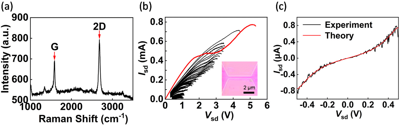 | ||
| Fig. 1 Graphene quantum dot devices fabricated by electroburning. (a) Standard Raman diagram of a single-layer graphene; compared with G peaks, the higher 2D peaks show a monolayer characteristic. (b) I–V curves of the feedback electroburning process; the red line is the curve of the first cycle, and the illustration is the graphene nanoribbon diagram under a microscope. (c) I–V curve after electroburning, obtained using the Simmons model to estimate the gap at 1–2 nm. | ||
We employ a feedback-controlled electroburning program to fracture the graphene ribbon under ambient conditions at room temperature. A voltage ramp of 1 V s−1 is applied to the source electrode, while monitoring and recording real-time current as well as maximum current during the process. Upon detection of a decrease in real-time current, the voltage is rapidly ramped down to 0 V within 1 ms. The feedback condition is adjusted based on the previous feedback threshold voltage. This iterative program continues until the low bias resistance between the source and drain electrodes exceeds 100 MΩ. Fig. 1b illustrates the source–drain current–voltage (I–V) curves obtained from this feedback process, where the red curve represents the I–V curve of the initial feedback breakage event. The inflection point of the red curve is related to the process of graphene annealing and impurity removal in an oxygen environment.29
The electroburning process culminates in the formation of gaps within the graphene ribbons, whose sizes are estimated using the Simmons model as depicted in Fig. 1c.30 Most of these gaps vary in size from 1 to 2 nm and may potentially contain graphene quantum dots. By comparing current maps as a function of source–drain voltage and gate voltage at 2 K temperature in a vacuum environment, these devices can be broadly classified into four groups.29Fig. 2a illustrates the transport properties of the nanogap without graphene quantum dots. The current map does not exhibit any discernible pattern, while the output characteristic curve shown in Fig. 2e (with a gate voltage of −2 V) demonstrates high symmetry that can be fitted using the Simmons model. Additionally, no prominent peak is observed in the transfer characteristic curve at a bias of −2 mV, as presented in Fig. 2i.
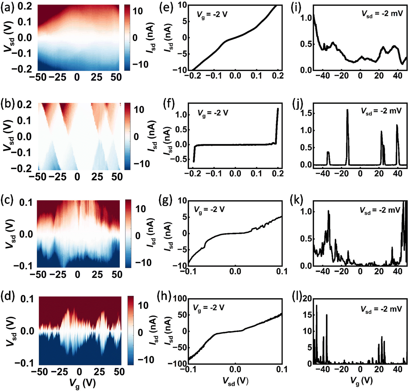 | ||
| Fig. 2 Four situations of graphene nanojunctions after electroburning. (a), (b), (c) and (d), respectively, show the differential conductance of the four types of graphene after electroburning. (a) No quantum dots in the graphene nanogap. (b) One quantum dot in the gap. (c) Multiple quantum dots in the gap. (d) The graphene ribbon is not completely broken. (e), (f), (g) and (h) show the output characteristic curves corresponding to the gate voltage of −2 V in the four cases, respectively; (i), (j), (k) and (l) show the transfer characteristic curves corresponding to the four cases when the bias is −2 mV. | ||
Fig. 2b illustrates the transport characteristics of a single graphene quantum dot within the nanogap. The current map exhibits a series of discernible rhombic blocking regions, characterized by equal slopes along their corresponding edges, commonly referred to as Coulomb diamonds.31 Under high bias conditions, electrons can traverse the boundaries of these Coulomb diamonds and enter the conduction region, resulting in an abrupt surge in current at specific bias voltages. Consequently, fitting the output characteristic curve at −2 V, as shown in Fig. 2f, using the Simmons model becomes challenging due to its deviation from the expected behaviour. Furthermore, the transfer characteristic curve at a bias of −2 mV in Fig. 2j exhibits a set of Coulomb peaks.
In Fig. 2c, the transport characteristics of multiple quantum dots within the graphene nanogap are depicted, revealing several sets of indistinguishable Coulomb diamonds with varying slopes. These diamonds correspond to abrupt points observed in the output characteristic curve at a gate voltage of −2 V in Fig. 2g and prove challenging to fit using the Simmons model. Additionally, multiple peaks can be observed in the transfer characteristic curve at a bias of −2 mV in Fig. 2k.
Fig. 2d illustrates the transport characteristics of graphene nanoribbons in a partially broken state, where multiple Coulomb diamonds are challenging to discern. In comparison with Fig. 2b and c, the size of the Coulomb diamonds is smaller while the current at both ends of the source and drain under identical bias voltage is larger. Notably, at a bias of −2 mV, Fig. 2l exhibits a transfer characteristic curve with more densely distributed peaks. The primary focus of this study is on the scenario depicted in Fig. 2b, specifically highlighting the presence of one quantum dot within the gap region.
Fig. 3 illustrates the differential conductance maps of four distinct graphene quantum dot devices under varying bias and gate voltages. The size estimation of a quantum dot can be achieved by analyzing the slopes and sizes of the Coulomb diamonds.32 The slopes of the diamond boundaries are determined using the ratio of the capacitances to the source (Cs), drain (Cd) and gate (Cg). The positive slopes α+ = Cg/(Cg + Cd) correspond to the case when the energy level of the quantum dot is aligned with the source. The negative slopes α− = Cg/(Cs) correspond to the case when the energy level of the quantum dot is aligned with the drain. Taking device A as an example, which is depicted in Fig. 3a, there are three complete Coulomb diamond regions within the gate voltage range from −50 V to 50 V. Notably, these three Coulomb diamonds possess identical absolute values for their slopes (α). When α+ = −α− = 0.018, it is concluded that the gate coupling parameter 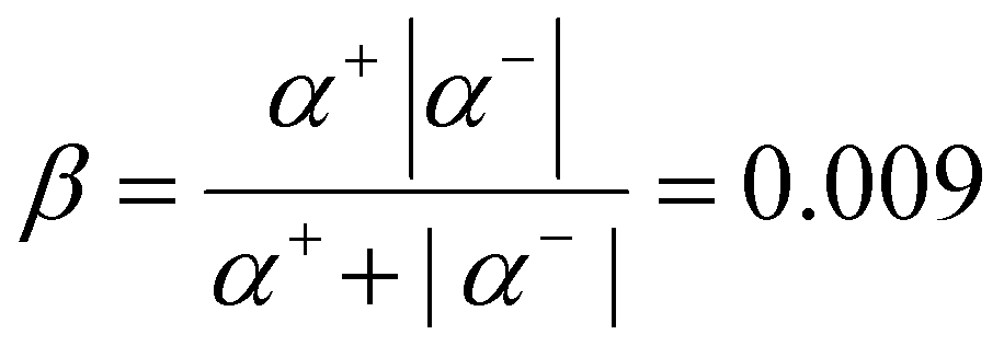 , which indicates the ability of the gate to regulate the energy level of the quantum dot. The height of the Coulomb diamond in Vsd multiplied by one electron charge (e) represents the energy required for adding a single electron to the quantum dot. This energy is commonly referred to as the addition energy (Eadd). The addition energy can be divided into two components: first, the charge energy Ec = e2/2C which accounts for overcoming the repulsion between charges within the quantum dot, where C = Cs + Cd + Cg is the total capacitance of the quantum dot, and second, ΔE, which denotes the difference in energy levels between the newly added electron and its predecessor. The size of the quantum dot can be estimated using two different methods with two kinds of energies. The Eadd values for the three Coulomb diamonds in Fig. 2a are 160 meV, 300 meV, and 140 meV, respectively. In this study, we assume a constant charging energy and consider multiple degenerate states within each energy level. Consequently, it can be inferred that a Coulomb diamond exhibiting a higher addition energy indicates electron occupation at an elevated energy level. Conversely, a Coulomb diamond with lower addition energy suggests electron filling in different degenerate states within the same energy level. The minimum Eadd = 140 meV is taken as the charging energy Ec to calculate the total capacitance of the quantum dot as C = e2/2Ec = 0.57 aF. The disk capacitance model was used to estimate the diameter of the graphene quantum dot dc = C/2(ε0(εoxide + εair)),33 where εoxide = 3.9 and εair = 1. The calculated result is 6.5 nm. In addition, the maximum Eadd = 300 meV minus the minimum Eadd = 140 meV can be defined as the energy level spacing ΔE = 160 meV, and dw = hvF/2ΔE = 13.7 nm can be estimated by using the two-dimensional quantum well model,23 where the Fermi velocity vF = 106 m s−1. Both of these estimation methods show that the diameter of the quantum dot in device A quantum dot is about 10 nm.
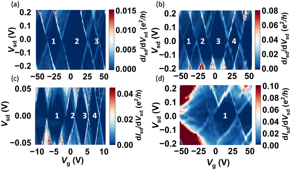 | ||
| Fig. 3 Differential conductance maps of graphene quantum dots with different sizes. (a), (b), (c) and (d) show the differential conductance of devices A, B, C and D, respectively. | ||
The relevant parameters of four different devices A, B, C and D are listed in Table 1. It can be seen that the gate coupling parameters of the four devices are all within the range of 0.01 ± 0.005, which reflects that the degree of adhesion between graphene quantum dots and silicon oxide substrates is relatively uniform to a certain extent. Due to the limitation of measurement conditions, there is only one complete Coulomb diamond, it is therefore impossible to judge the specific electron filling of quantum dot D, and the Eadd of the Coulomb diamond is regarded as Ec. The absolute values of the positive and negative slopes of device D are different, which indicates the asymmetry of electron transport between the source and drain.
| Device Number | α + | α − | β | E c (meV) | ΔE (meV) | C (aF) | d c (nm) | d w (nm) |
|---|---|---|---|---|---|---|---|---|
| The information includes the following: the device number; the positive slope of the Coulomb diamond: α+; the negative slope of the Coulomb diamond: α−; the gate coupling coefficient: β; the charge energy: Ec; the energy level spacing: ΔE; the total capacitance of the quantum dot: C; the diameter of the graphene quantum dot estimated with the disk capacitance model: dc; the diameter of the graphene quantum dot estimated with the two-dimensional quantum well model: dw. | ||||||||
| A | 0.018 | −0.018 | 0.009 | 140 | 160 | 0.57 | 6.5 | 13.7 |
| B | 0.02 | −0.02 | 0.01 | 130 | 120 | 0.6 | 6.7 | 17 |
| C | 0.03 | −0.03 | 0.015 | 40 | 50 | 2 | 22 | 41 |
| D | 0.0077 | −0.015 | 0.005 | 170 | — | 0.47 | 5.3 | — |
Compared with the sizes of the devices A, B and D (about 10 nm), the differential conductance map of device C shows smaller Coulomb diamonds and correspondingly a larger quantum dot. This phenomenon shows that the larger the size of the quantum dot, the smaller the repulsion of the internal electrons, and therefore the smaller the addition energy required to add an electron to the quantum dot. At the same time, the increase of quantum dot size makes the energy level spacing decrease, which is consistent with the transformation law from the energy level of microscopic molecules to the energy band of macroscopic objects.
By applying a perpendicular magnetic field to the graphene dot at a bias of 2 mV, we observed anomalous changes in conductance at the point of resonance tunneling. These changes exhibit high repeatability, effectively eliminating the impact of thermal and electrical noise. We measured the 0–8 T magnetic response curves of each Coulomb peak in device C (Fig. 4a–e), revealing that each peak displays distinct responses while changing the magnetic fields. However, there are no significant changes in the central position of the peak, ruling out any Zeeman effect caused by intrinsic magnetic moments of quantum dots.34 We attribute this unusual magnetic response to the fluctuation of density of states of the graphene leads caused by both applied electrical and magnetic fields.35
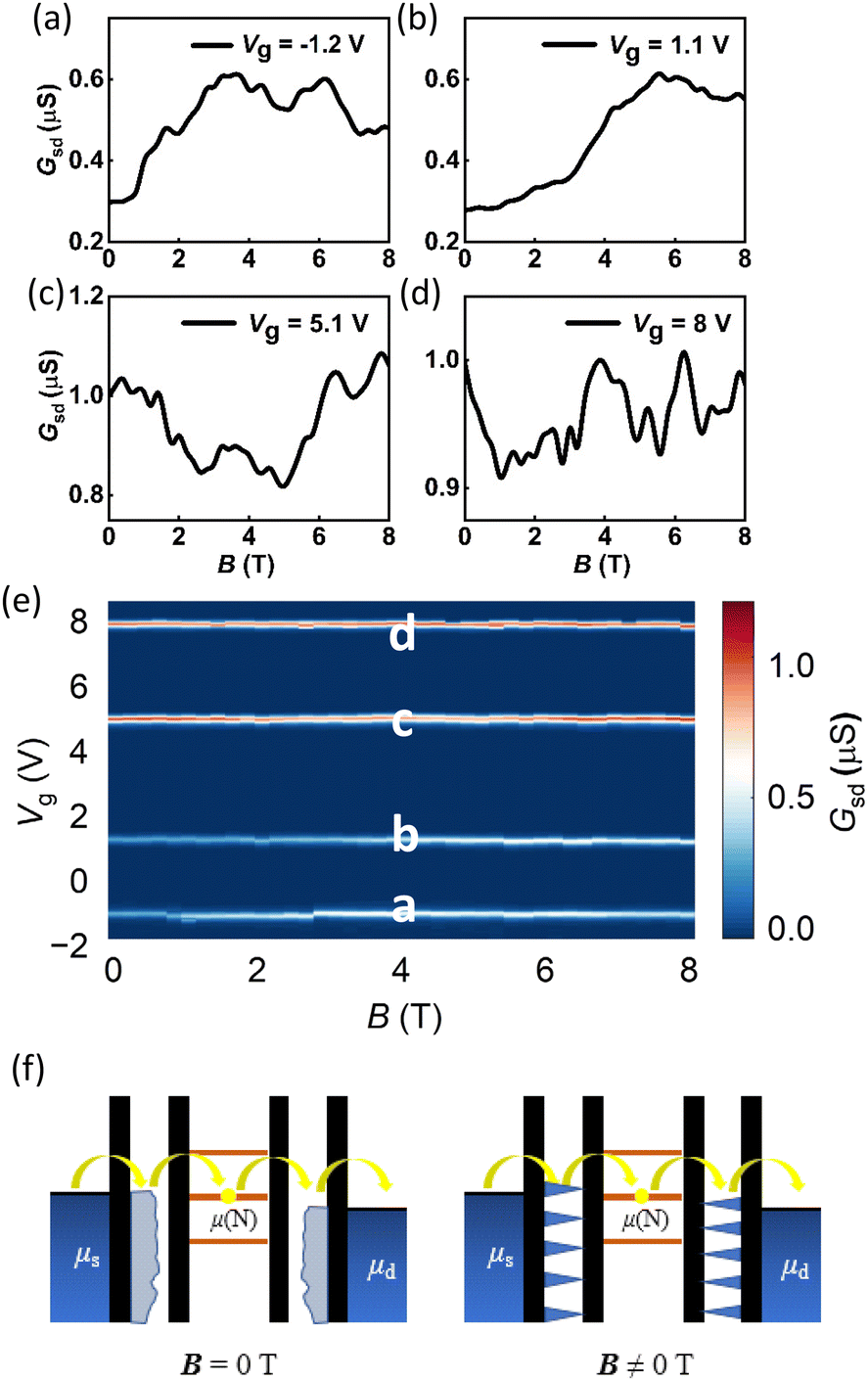 | ||
| Fig. 4 Conductance change of device C in a magnetic field. (a), (b), (c) and (d) show the conductance and applied vertical magnetic field relationship of device C. The bias voltage is 2 mV, the magnetic field range is 0 to 8 T, and the gate voltage is −1.2 V, 1.1 V, 5.1 V, and 8 V, respectively. (e) The variation of the current of device C at the four Coulomb peak with the magnetic field, ranging from 0 to 8 T. (f) Schematic diagram showing magnetoconductance changes of graphene quantum dots. The leads at both ends of graphene quantum dots form Landau energy levels in magnetic fields, and the density of states changes. | ||
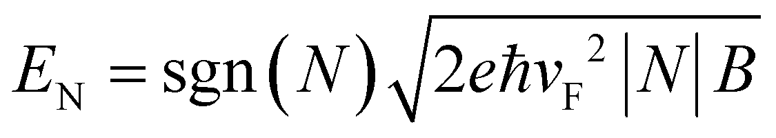
As a unique two-dimensional material, graphene exhibits quantized energy levels under strong magnetic fields, resulting in the formation of Landau levels as depicted in Fig. 4f.36,37 The Landau level energy of the zero-mass Dirac fermion in graphene is as follows:3
 | (1) |
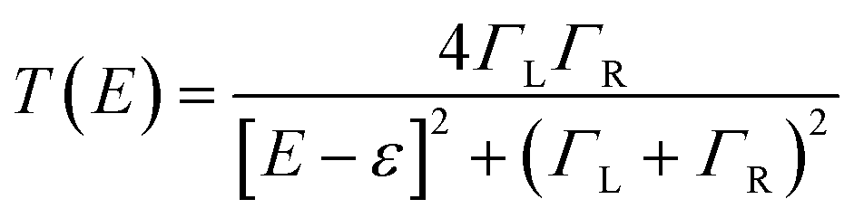
To illustrate the relationship between the density of states of the leads and the conductance, the current through a certain energy level orbital of a quantum dot is given by the Landau equation35
 | (2) |
 | (3) |
In conclusion, we present a detailed procedure for synthesizing graphene quantum dots through electroburning and investigate the Coulomb blockade phenomenon at low temperatures. By employing the disk capacitance model and two-dimensional quantum well model, we estimate the diameters of various quantum dots, which range from a few to tens of nanometers. Furthermore, upon applying a vertical magnetic field, we observe significant changes in conductance attributed to variations in the Landau level within the graphene leads located at both ends of the quantum dot at the Fermi surface. Notably, adjusting the gate voltage allows for the regulation of the Fermi level within these leads, resulting in distinct conductance trends. It is crucial to acknowledge that this lead effect may potentially interfere with future analyses involving magnetic responses in graphene-based single-molecule transistors, thus necessitating comprehensive theoretical investigations aimed at mitigating such interference.
Conflicts of interest
There are no conflicts to declare.Acknowledgements
We acknowledge the financial support of the National Key R&D Program of China (Grant no. 2022YFA1402), the National Natural Science Foundation of China (Grant no. 92161201, T2221003, 12104221, 12104220, 12274208, 12025404 and 91961101), and the Fundamental Research Funds for the Central Universities (Grant no. 020414380192).References
- K. S. Novoselov, A. K. Geim and S. V. Morozov, et al., Electric Field Effect in Atomically Thin Carbon Films, Science, 2004, 306(5696), 666–669 CrossRef CAS PubMed.
- A. K. Geim and K. S. Novoselov, The rise of graphene, Nat. Mater., 2007, 6(3), 183–191 CrossRef CAS PubMed.
- Y. Zhang, Y.-W. Tan and H. L. Stormer, et al., Experimental observation of the quantum Hall effect and Berry's phase in graphene, Nature, 2005, 438(7065), 201–204 CrossRef CAS PubMed.
- A. F. Young and P. Kim, Quantum interference and Klein tunnelling in graphene heterojunctions, Nat. Phys., 2009, 5(3), 222–226 Search PubMed.
- K. Kim, J.-Y. Choi and T. Kim, et al., A role for graphene in silicon-based semiconductor devices, Nature, 2011, 479(7373), 338–344 CrossRef CAS PubMed.
- F. Prins, A. Barreiro and J. W. Ruitenberg, et al., Room-Temperature Gating of Molecular Junctions Using Few-Layer Graphene Nanogap Electrodes, Nano Lett., 2011, 11(11), 4607–4611 CrossRef CAS PubMed.
- C. S. Lau, J. A. Mol and J. H. Warner, et al., Nanoscale control of graphene electrodes, Phys. Chem. Chem. Phys., 2014, 16(38), 20398–20401 RSC.
- H. Sadeghi, J. A. Mol and C. S. Lau, et al., Conductance enlargement in picoscale electroburnt graphene nanojunctions, Proc. Natl. Acad. Sci. U. S. A., 2015, 112(9), 2658–2663 CrossRef CAS PubMed.
- P. Gehring, H. Sadeghi and S. Sangtarash, et al., Quantum Interference in Graphene Nanoconstrictions, Nano Lett., 2016, 16(7), 4210–4216 CrossRef CAS PubMed.
- J. O. Island, A. Holovchenko and M. Koole, et al., Fabrication of hybrid molecular devices using multi-layer graphene break junctions, J. Phys.: Condens. Matter, 2014, 26(47), 474205 CrossRef CAS PubMed.
- D. Xiang, X. Wang and C. Jia, et al., Molecular-Scale Electronics: From Concept to Function, Chem. Rev., 2016, 116(7), 4318–4440 CrossRef CAS PubMed.
- J. A. Mol, C. S. Lau and W. J. M. Lewis, et al., Graphene-porphyrin single-molecule transistors, Nanoscale, 2015, 7(31), 13181–13185 RSC.
- K. Ullmann, P. B. Coto and S. Leitherer, et al., Single-Molecule Junctions with Epitaxial Graphene Nanoelectrodes, Nano Lett., 2015, 15(5), 3512–3518 CrossRef CAS PubMed.
- E. Burzurí, J. O. Island and R. Díaz-Torres, et al., Sequential Electron Transport and Vibrational Excitations in an Organic Molecule Coupled to Few-Layer Graphene Electrodes, ACS Nano, 2016, 10(2), 2521–2527 CrossRef PubMed.
- T. Pei, J. O. Thomas and S. Sopp, et al., Exchange-induced spin polarization in a single magnetic molecule junction, Nat. Commun., 2022, 13(1), 4506 CrossRef CAS PubMed.
- Z. Chen, J.-R. Deng and S. Hou, et al., Phase-Coherent Charge Transport through a Porphyrin Nanoribbon, J. Am. Chem. Soc., 2023, 145(28), 15265–15274 CrossRef CAS PubMed.
- W. Niu, S. Sopp and A. Lodi, et al., Exceptionally clean single-electron transistors from solutions of molecular graphene nanoribbons, Nat. Mater., 2023, 22(2), 180–185 CrossRef CAS PubMed.
- Y. Cao, S. Dong and S. Liu, et al., Building High–Throughput Molecular Junctions Using Indented Graphene Point Contacts, Angew. Chem., Int. Ed., 2012, 51(49), 12228–12232 CrossRef CAS PubMed.
- C. Jia and X. Guo, Molecule–electrode interfaces in molecular electronic devices, Chem. Soc. Rev., 2013, 42(13), 5642 RSC.
- Q. Xu, G. Scuri and C. Mathewson, et al., Single Electron Transistor with Single Aromatic Ring Molecule Covalently Connected to Graphene Nanogaps, Nano Lett., 2017, 17(9), 5335–5341 CrossRef CAS PubMed.
- P. Puczkarski, P. Gehring and C. S. Lau, et al., Three-terminal graphene single-electron transistor fabricated using feedback-controlled electroburning, Appl. Phys. Lett., 2015, 107(13), 133105 CrossRef.
- J. Moser and A. Bachtold, Fabrication of large addition energy quantum dots in graphene, Appl. Phys. Lett., 2009, 95(17), 173506 CrossRef.
- A. Barreiro, H. S. J. van der Zant and L. M. K. Vandersypen, Quantum Dots at Room Temperature Carved out from Few-Layer Graphene, Nano Lett., 2012, 12(12), 6096–6100 CrossRef CAS PubMed.
- P. Recher, J. Nilsson and G. Burkard, et al., Bound states and magnetic field induced valley splitting in gate-tunable graphene quantum dots, Phys. Rev. B: Condens. Matter Mater. Phys., 2009, 79(8), 085407 CrossRef.
- S. Schnez, F. Molitor and C. Stampfer, et al., Observation of excited states in a graphene quantum dot, Appl. Phys. Lett., 2009, 94(1), 012107 CrossRef.
- R. K. Puddy, C. J. Chua and M. R. Buitelaar, Transport spectroscopy of a graphene quantum dot fabricated by atomic force microscope nanolithography, Appl. Phys. Lett., 2013, 103(18), 183117 CrossRef.
- D. Bischoff, A. Varlet and P. Simonet, et al., Localized charge carriers in graphene nanodevices, Appl. Phys. Rev., 2015, 2(3), 031301 Search PubMed.
- J. Shen, Y. Zhu and X. Yang, et al., Graphene quantum dots: emergent nanolights for bioimaging, sensors, catalysis and photovoltaic devices, Chem. Commun., 2012, 48(31), 3686 RSC.
- B. Limburg, J. O. Thomas and G. Holloway, et al., Anchor Groups for Graphene–Porphyrin Single–Molecule Transistors, Adv. Funct. Mater., 2018, 28(45), 1803629 CrossRef.
- J. G. Simmons, Generalized Formula for the Electric Tunnel Effect between Similar Electrodes Separated by a Thin Insulating Film, J. Appl. Phys., 1963, 34(6), 1793–1803 CrossRef.
- C. C. Escott, F. A. Zwanenburg and A. Morello, Resonant tunnelling features in quantum dots, Nanotechnology, 2010, 21(27), 274018 CrossRef CAS PubMed.
- E. A. Osorio, T. Bjørnholm and J. M. Lehn, et al., Single-molecule transport in three-terminal devices, J. Phys.: Condens. Matter, 2008, 20(37), 374121 CrossRef CAS PubMed.
- B. Gelmont, M. S. Shur and R. J. Mattauch, Disk and stripe capacitances, Solid-State Electron., 1995, 38(3), 731–734 CrossRef CAS.
- Z. Ge, S. Slizovskiy and P. Polizogopoulos, et al., Giant orbital magnetic moments and paramagnetic shift in artificial relativistic atoms and molecules, Nat. Nanotechnol., 2023, 18(3), 250–256 CrossRef CAS PubMed.
- P. Gehring, J. K. Sowa and J. Cremers, et al., Distinguishing Lead and Molecule States in Graphene-Based Single-Electron Transistors, ACS Nano, 2017, 11(6), 5325–5331 CrossRef CAS PubMed.
- S. Schnez, K. Ensslin and M. Sigrist, et al., Analytic model of the energy spectrum of a graphene quantum dot in a perpendicular magnetic field, Phys. Rev. B: Condens. Matter Mater. Phys., 2008, 78(19), 195427 CrossRef.
- M. O. Goerbig, Electronic properties of graphene in a strong magnetic field, Rev. Mod. Phys., 2011, 83(4), 1193–1243 CrossRef CAS.
- D.-K. Ki and A. F. Morpurgo, Crossover from Coulomb Blockade to Quantum Hall Effect in Suspended Graphene Nanoribbons, Phys. Rev. Lett., 2012, 108(26), 266601 CrossRef PubMed.
- H. T. Man and A. F. Morpurgo, Sample-Specific and Ensemble-Averaged Magnetoconductance of Individual Single-Wall Carbon Nanotubes, Phys. Rev. Lett., 2005, 95(2), 026801 CrossRef CAS PubMed.
- J. Kong, E. Yenilmez and T. W. Tombler, et al., Quantum Interference and Ballistic Transmission in Nanotube Electron Waveguides, Phys. Rev. Lett., 2001, 87(10), 106801 CrossRef CAS PubMed.
- D. Bischoff, F. Libisch and J. Burgdörfer, et al., Characterizing wave functions in graphene nanodevices: Electronic transport through ultrashort graphene constrictions on a boron nitride substrate, Phys. Rev. B: Condens. Matter Mater. Phys., 2014, 90(11), 115405 CrossRef.
Footnotes |
| † Electronic supplementary information (ESI) available. See DOI: https://doi.org/10.1039/d3nr06176k |
| ‡ These authors contributed equally to this work. |
| This journal is © The Royal Society of Chemistry 2024 |