
Role of defects and exposed graphene in carbon nanomaterial-based electrocatalysts
Charles C.
Chusuei
 * and
Ram Chandra
Nepal
* and
Ram Chandra
Nepal
Chemistry Department, Middle Tennessee State University, 440 Friendship Street, Murfreesoboro, TN 37132, USA. E-mail: Charles.Chusuei@mtsu.edu; Tel: +1-615-898-2079
First published on 4th December 2023
Abstract
Carbon nanomaterials (CNMs, carbon dots, carbon nanotubes, and graphene) have received much attention in recent decades for their technological roles as electrocatalysts for biosensing and fuel cell applications in aqueous solutions. Their complex form factor presents challenges for delineating structure–property relationships, namely the interplay of electroactive area surface defects and exposed graphene planar structure, for optimizing their electrocatalytic activity. Conflicting examples in the literature show higher defect density in the graphene structure with increased or decreased conduction of the material. The graphenyl sheet curvature, voltage range of the electrochemical redox reaction, dispersion of charged impurities affecting the charge mobility, and overall resistivity of the CNM materials should be considered to optimize the overall electrochemical activity, particularly as they relate to redox reactions taking place in the −0.2 to +0.3 V standard potential range.
1. Introduction
CNMs (carbon dots, carbon nanotubes, and graphene) have received much attention in the last few decades for their technological roles as electrocatalysts for biosensing and fuel cell applications in aqueous solutions. Due to their often ill-defined morphology and form factor, there are challenges in delineating structure–property relationships involving the interplay of electroactive area surface defects and exposed graphene planar structure for optimizing their electrocatalytic activity. Nanostructured carbon has been widely used as electrocatalysts due to its low cost, high specific surface area, and carrier mobility.1,2 Graphene is the two-dimensional building block for sp2 carbon allotropes for all other dimensionalities within these structures. Graphene can be stacked into three-dimensional graphite, rolled into one-dimensional nanotubes, or involved in building blocks of zero-dimensional carbon dots. Raman spectroscopy has been a staple for fast, non-destructive, high-resolution characterization of the electronic structure of CNM supports.3–5 Theoretically, defects enhance conduction by creating electron acceptors in the graphene structure.6,7 Examples of defects (resulting from undesired effects of transferring graphene from metallic to non-metallic substrates) include corrugation, cracks, metal and polymer residuals, and oxygen-containing functional groups chemically bonded to the sp2-hybridized graphene sheet.8However, some experiments show defects hampering rather than enhancing conduction.7 Why is it that in some cases, electrochemical current reading increases with higher CNM defect density while in others, they do not? The answer lies with the location of the Fermi level (EF) relative to the measurement made (vide infra). An interplay between defect density and reactant exposure to graphene sheets influences the optimization of these electrocatalyst materials. The presence of charge carriers within the CNMs also play a role in their conductive properties.
2. Characterizing graphene and sheets in carbon nanomaterials
The chief tools widely used to characterize graphene and its defect structures within carbon nanomaterials are Raman and photoelectron spectroscopies, and electron microscopy. Ultrasonication has the effect of both introducing defects and increasing graphene sheet exposure in multi-walled carbon nanotubes. In the early development of carbon nanomaterial electrocatalysts, multi-walled carbon nanotubes (MWCNTs) were functionalized in our laboratory to enable the attachment of catalytically active nanoparticles for sensing and fuel cell performance. Xing et al.9 showed that MWCNTs could be functionalized with carboxylate groups in a controlled fashion, in which total ultrasonication time was directly proportional to the number of functional groups attached to the sidewalls. While this early study did not rely on Raman to make the assessment of introduced defects, transmission electron microscopy (TEM) and X-ray photoelectron spectroscopy (XPS) did, revealing roughening of the MWCNT sidewalls (creating sp3 sites) and the concomitant increase of O-containing functional groups as measured by integrated areas of the XPS O 1s core levels (Fig. 1A and B). Fig. 1a through c show TEM images of the MWCNTs after 2, 4, and 8 h of sonication, respectively. As sonication time increased, so did the roughening of the MWCNT sidewalls and the appearance of additional functional groups denoted by the development in higher binding energy XPS C 1s chemical oxidation states. Within a 0-to-8 h sonication treatment period, defect density increased (as shown in the Raman spectra, Fig. 1A and B), with the optimum density of functionalization and defect formation occurring at approximately 2 h. The growth of the Raman D band (relative to the G band) plateaued at a 2 h sonication treatment, shown in a subsequent study.10 Conditions for this sonication treatment were mild, precluding any flattening effects that would have affected the D band intensity. Quantitative density measurements of the D band (sp3 carbon) were normalized by division of the sp2 carbon by the G band integrated peak area. In examining the ID/IG ratios, the disordered sp3 state increased with longer sonication treatment plateauing at 2 h. ID/IG intensities matched the reported increasing trend of atom % O tethered to the MWCNT sidewall as quantified by XPS O 1s high-resolution scans. The Raman ID/IG ratios agree with functional group saturation occurring at the 2 h sonication time. A direct correlation exists between the amount of disordered-to-ordered carbon with –COO–/–CO–/–C![[double bond, length as m-dash]](https://www.rsc.org/images/entities/char_e001.gif) O surface density growth on the MWCNT sidewalls.
O surface density growth on the MWCNT sidewalls.
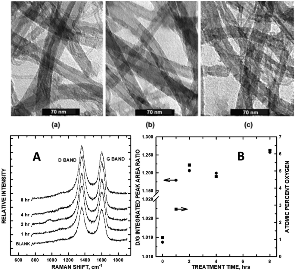 | ||
| Fig. 1 (top) TEM of MWCNTs after (a) 2 h, (b) 4 h, and (c) 8 h of sonication; (bottom) (A) Raman spectra of 1-through-8 h sonicated MWCNTs. (B) Integrated Raman D/G peak areas (left axis) and atomic % oxygen (right axis) vs. sonication time. Reprinted from ref. 9 and 10 (Copyright 2005 and 2006, respectively) with permission from the American Chemical Society. | ||
The defect density within the graphene sheets reached a plateau at the 2 h mark. The kinetic growth of the O-containing functional groups that precisely matched with sonication time and D/G band growth (and subsequent plateauing) corroborates this conclusion within the study. Since functionalization directly correlated with the growth of sp3 carbon in the Raman analysis, we conclude that defectsindirectly increase electrocatalytic activity on the CNM surface by enabling the tethering of Pt nanoparticles (NPs) in a way that minimizes aggregation and, hence, in the case of the direct methanol fuel cell reaction (vide infra), increases the surface area of adsorbed Pt for redox reactions.
The Raman D-band results from the radial breathing modes of six-atom rings and require defects (topological imperfections, such as vacancies, edges, pores, etc.) for its activation;11 the D′, 2D, and 2D′ peaks are overtones of the defects.12 The Raman G band denotes the graphene sp2-hybridized carbon. Raman can distinguish between a hard amorphous carbon, a metallic nanotube, and doped graphene.13 Density functional theory (DFT) calculations predict that defects within the 2D structures increase electron transfer at the aqueous solution-solid surface interface, resulting in greater conductivity since defects increase activity by serving as electron acceptors from adsorbed metal nanoparticles or from analyte materials as they undergo solution redox.14 But, this observation is not universal since increases in defect density have been correlated with decreased current response in some instances,7,14 including those examples that will be discussed in section 5 of this article.
A caveat that should be noted is that flattened graphene structures within multiwalled carbon nanotubes have been reported to have a marked D-band intensity without introducing defects by Picheau et al.15 where variances in graphene curvature contribute to observed D band intensity.16 The phenomenon is observed for carbon nanotubes with a single or a few walls. Nanotubes at a critical diameter (greater than 5 nm) spontaneously collapse and create folds, enhancing D band intensity. In this experiment, the end caps of the MWCNTs were cut, and the inner concentric nanotubes were removed, flattening the remaining structure. The defect density of the outer-most walls was constant, but the D band intensity increased (Fig. 2)!15 Indeed, characterizing exposed graphene defects becomes more nuanced with this discovery and invites questions regarding CNM composite fabrication for optimized electrochemical performance.
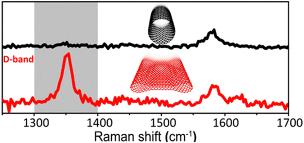 | ||
| Fig. 2 Raman spectra of flattened and unflattened MWCNTs. Reprinted from ref. 15 (Copyright 2021) with permission from the American Chemical Society. | ||
For single-walled CNTs where Raman signals of peaks of the overtones would be more visible, defect density and graphene sheet exposure can be monitored using the D, G, D′, and 2D bands that appear at ca. 1330, 1580, 1615, and 2675 cm−1.17,18 The increase in defect density can be exhibited by splitting the primary G band into the G band, along with a resolved D′ band, observed at ca. 1560 cm−1.5 The D′ band may be subsumed within the G-band in cases where this feature is not well-resolved; its intensity is convoluted within the G band intensity.
3. Defects enhance heterogeneous electron transfer at voltages between −0.2 to +0.3 V
A landmark study of the influence of defects on electrocatalytic activity by Kislenko et al.13 showed that in defect-induced mid-gap states that catalyze electron transfer reactions at non-adiabatic conditions, the electrochemical response is defect dependent. Ab initio calculations show significant electron transfer occurring for monovalencies (relative to pristine graphene with no defects) for redox coupled standard potentials ranging from −0.2 to +0.3 V (versus the standard hydrogen electrode, aka the ‘Kislenko range’) in density functional theory (DFT) investigations using the Gerischer model, which considers quantum capacitance. The zero voltage measured under aqueous solution conditions denotes the effective location of EF. It is within this voltage range, close to EF, that redox couples overlap with the electronic states of graphene. Beyond the −0.2 to +0.3 V, the role of defects in electrical conduction greatly diminishes. Experimental evidence by other researchers is largely in agreement with this DFT prediction.In a study by Slate et al.19 on the electrochemical performance of graphite and graphene paste electrodes, greater electrochemical activity was observed with later lateral flake sizes as observed in the TEM and correlating with 1 mM hexaammineruthenium(II) chloride as a redox probe, denoting sp2 graphene sheets. Smaller flake size improved heterogeneous electron transfer (HET) kinetics. The beneficial resonance was due to the increased number of edge plane-like sites on the electrode surface. Density functional theory (DFT) showed that coverage of the edge plane-like sites led to greater electrochemical performance. Insight from this work shows that the flattening of the MWCNTs in Picheau et al.'s15 study resulted in the D-band enhancement due to greater exposure of the defects for Raman detection (Fig. 2). This interpretation is consistent with defects acting as electron acceptors, giving rise to increased conductivity while simultaneously having greater exposure to the graphene sp2 carbon.
Noteworthy is that in cases with substantial changes in graphene sheet curvature, Picheau et al.'s15 findings also indicate that normalization of defect density measurements from Raman spectra by dividing the D-band integrated peak area intensity by that of the G-band, under these conditions, is unreliable. Raman scattering from folds in a single-layer graphene sheet has been known to arise from spatially inhomogeneous curvature around a fold within the graphene sheet, resulting in an enhanced D band.16 In addition, wrinkling and crumpling in twisted few and multilayer graphene have increased the integrated area under the D Raman band.20 In such cases where there are severe distortions in the curvature and/or crumpling of the graphene sheet structure, complementary experimental evidence should be used to corroborate defect density changes to increase conductivity. So long as the curvature of the CNM is not affected, we postulate that defects enhance conductivity for those electrochemical reactions occurring between −0.2 and +0.3 V.
One such example is that of a Prussian Blue (PB) electrodeposited onto a glassy carbon modified with zirconia-doped functionalized carbon nanotubes (PB/ZrO2-fCNTs/GC), giving rise to enhanced sensitivity for H2O2 detection,21 in which redox activity for H2O2 was observed at +0.2 V. With functionalization, the defect density of the PB/ZrO2-fCNTs/GC increased as observed in the Raman spectra, accompanying enhanced signal for detecting the H2O2 analyte.
The three-dimensional porous and redox-active Prussian Blue in graphene (PB@G) to aerogels with mass ratios of 2.5![[thin space (1/6-em)]](https://www.rsc.org/images/entities/char_2009.gif) :1 to 1:2.5 show enhanced redox activity for H2O2 detection accompanying increased defect density as observed by Raman spectroscopy.22 XPS core level shifts of the C 1s orbital showed an increased number of oxidation states, accompanying greater PB loading and, subsequently, larger D band populations. The Raman ID/IG ratios of this series of PB-loaded graphene aerogels (with the graphene-to-PB loadings) for the pristine graphene aerogel, 2.5:1 G:PB, 1:1 G:PB, and 1:1.25 G:PB were 2.16, 1.17, 2.17, 2.02, respectively. The steepest slope for the current increase was obtained for the electrode with the largest density of electrodeposited PB to detect H2O2. These redox peaks were within the −0.2 to +0.3 V range. The largest current observed for the reduction of H2O2 was observed with a detection limit of 5 nM for the analyte with the largest ID/IG band ratio.
:1 to 1:2.5 show enhanced redox activity for H2O2 detection accompanying increased defect density as observed by Raman spectroscopy.22 XPS core level shifts of the C 1s orbital showed an increased number of oxidation states, accompanying greater PB loading and, subsequently, larger D band populations. The Raman ID/IG ratios of this series of PB-loaded graphene aerogels (with the graphene-to-PB loadings) for the pristine graphene aerogel, 2.5:1 G:PB, 1:1 G:PB, and 1:1.25 G:PB were 2.16, 1.17, 2.17, 2.02, respectively. The steepest slope for the current increase was obtained for the electrode with the largest density of electrodeposited PB to detect H2O2. These redox peaks were within the −0.2 to +0.3 V range. The largest current observed for the reduction of H2O2 was observed with a detection limit of 5 nM for the analyte with the largest ID/IG band ratio.
In addition, PB tethered to graphene (PB/GE) showed an enhanced reduction of H2O2; within this system, PB introduced defects onto the graphene sheet for a four-electron oxygen reduction in acidic media for the oxygen reduction reaction (ORR), important for fuel cell reactions.23 A higher ID/IG band ratio (in parentheses), accompanying higher measure current using the cyclic voltammetry (CV) peak-to-peak height, was observed for PB/GE (1.95) than for graphene (GE) (1.92) deposited on the glassy carbon working electrode (GCE) and is consistent with the prediction by Kislenko et al.13 for the observed standard reduction voltage of +0.2 V (Fig. 3).
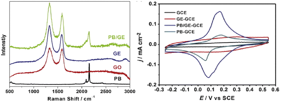 | ||
| Fig. 3 (A) Raman stack plot of the PB, GE, GO, and PB/GE; (B) CVs of the GCE, GE–GCE, PB/GE–GCE, and PB–GCE. Reprinted from ref. 23 (Copyright 2013) with permission from Elsevier. | ||
PB deposited on graphene oxide within a graphene oxide/PB/glucose oxidase/chitosan composite showed enhanced sensitivity for detecting H2O2 with a 1.2 × 10⁻⁷ M detection limit. Redox peak current intensities for voltages within the −0.2 to +0.3 V (with Raman ID/IG values in parentheses) were seen in the following descending order: GO/PB (2.137) > GO (1.799) > PB.24 (The bare PB had no D or G Raman bands.) The higher defect density electrocatalyst exhibited greater sensitivity to glucose. For PB introduced to reduced graphene oxide/multi-walled carbon nanotube (RGO/MWCNT) composites, Silva et al.25 reported increased current at a +0.2 V standard potential for the detection of ClO− and H2O2 for reduced PB/RGO/MWCNTs as compared to RGO/MWCNTs. As with the previous example, the increased sensitivity for analyte detection accompanied the increase of defects for redox activity within the Kislenko range. The ID/IG ratio for the composites with and without PB were 2.92 and 2.47, respectively (Fig. 4).
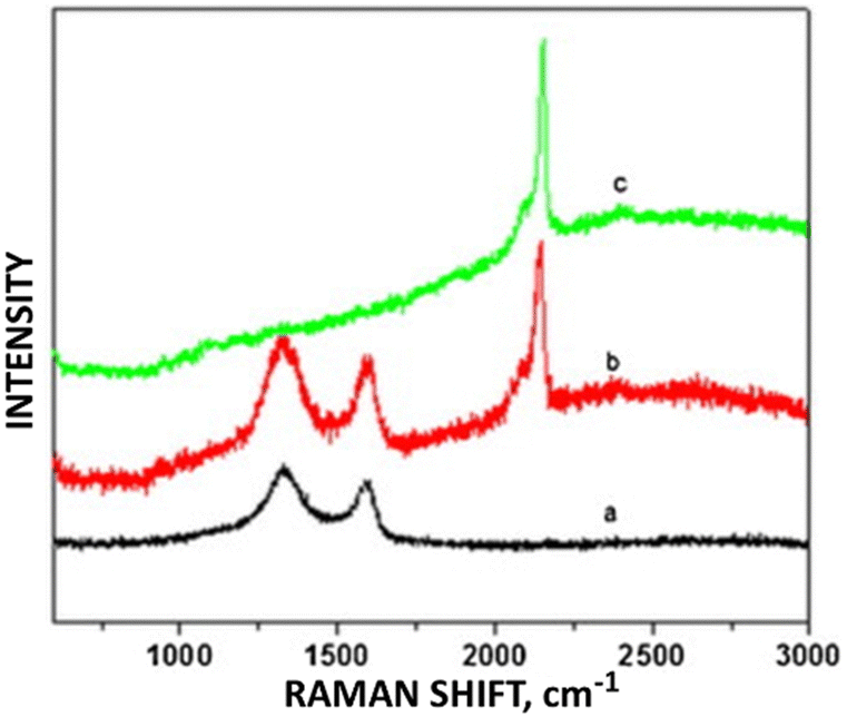 | ||
| Fig. 4 Raman stack plot of (a) GO, (b) GO/PB, and (c) PB. Reprinted from ref. 24 (Copyright 2011) with permission from Elsevier. | ||
In the case of PB adsorbed onto ZnO nanoparticles tethered to carboxylic acid functionalized carbon nanotubes (PB/ZnO/COOH-MWCNTs) in our laboratory, the introduction of defects accompanied the increase in electrochemical sensing current for the detection of H2O2 in phosphate buffer solution at pH 7.26Fig. 5A shows control CV experiment of 5 mM H2O2 in phosphate buffer solution exposed to PB/ZnO/COOH-MWCNTs and subsets of this composite (see figure caption for details). The CV peak-to-peak height showed a 2.7-fold increase in current density between ZnO/COOH-MWCNTs and PB/ZnO/COOH-MWCNTs. The corresponding ID/IG ratios for ZnO/COOH-MWCNTs and PB/ZnO/COOH-MWCNTs were 0.733 and 0.940 (Fig. 5B), respectively, corresponding with a 1.3-fold increase in defect sites (Fig. 5A). The composite with the larger defect density exhibited the highest current for H2O2 detection. The APAP CV signal increased with increasing sp3 carbon density. Regarding the predicted trend according to the Kislenko range, the oxidation current of ZnO/COOH-MWCNTs was slightly outside the prescribed range with respect to measured current with applied voltage. The oxidation peak shifted from −0.341 V (outside the range) to +0.0004 V (within the range) within the CV data. Yet, in this single instance where the oxidation potential was outside the prescribed range, the defect density population (sp3 carbon) still accurately predicted the current increase.
 | ||
| Fig. 5 (A) CVs of 5 mM H2O2 in phosphate buffer solution (PBS) (pH 7) using (a) PB/ZnO/COOH-MWCNTs and (b) ZnO/COOH-MWNTs; (c) CV of PBS using PB/ZnO/COOH-MWCNTs, (d) CV of 5 mM H2O2 using PB, and (d) CV of 5 mM H2O2 in PBS on the bare GCE; (B) Raman stack plot of (a) ZnO/COOH-MWCNTs and (b) PB/ZnO/COOH-MWCNTs. Fig. 5A is reprinted from ref. 26 (Copyright 2019) with permission from the American Chemical Society. Fig. 5B was newly acquired by the authors of this Focus article. | ||
4. Impurities in graphene introduce charge mobility, which can be hampered by defects, decreasing conductivity
The presence of charged impurities can skew the proportionality of defect density to electrical conduction, in which defects hamper charge mobility instead of serving as electron acceptors. In this case, an increase in defect density would reduce conductivity. Experiments by Salehi et al.18 showed that healing defect structures on graphene via exposure to a plasma of methane and hydrogen to remove oxygen-containing functional groups resulted in highly conductive graphene. Optical emission spectroscopy and atomic force micrographs of the resulting smooth graphene surface (revealing fewer defects) showed a correlation between the elimination of defects with increased conductivity. The increase in conduction spanned the −1.0 to +1.0 V range.The example of Fe2O3 and PB incorporated into an MWCNT composite for the oxidation reaction of 500 μM H2O2 (demonstrating its electrochemical sensing capabilities) was observed at +0.1 V.27 The ∼15% increase in current was accompanied by a decrease in defect density from the PB nanoparticles in the Fe2O3/MWCNT@PB electrocatalyst support, as observed in the Raman data (Fig. 6). Comparing the Raman spectra in the stack plot between Fe2O3/MWCNTs with that of Fe2O3/MWCNTs@PB, when the PB was introduced, the D′ peak at ca. 1550 cm−1, denoting the increase in defect density on the graphene sheet, which accompanied the decrease in peak-to-peak height signal observed in the corresponding CVs of these composites as 500 μM H2O2 was detected when comparing the CV in Fig. 6b (right) with this same composite Fig. 6a (right) without H2O2. The ID/IG ratios of the MWCNT-Fe2O3@PB, MWCNT-Fe2O3, and MWCNT were 0.444, 0469, and 0.671, respectively (Fig. 6, left). The Raman shift at ca. 2150 cm−1 is an experimental artifact of the PB. The peak at 2154.79 cm−1 is an experiment artifact of the Fe(III)–CN–Fe(II) additive used.
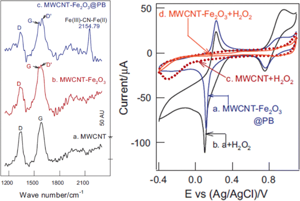 | ||
| Fig. 6 (Left) Raman stack plot of (a) MWCNT, (b) MWCNT-Fe2O3, and (c) MWCNT-Fe2O3@PB; (right) CVs of (a) MWCNT-Fe2O3@PB, (b) a + H2O2, (c) MWCNT + H2O2, and (d) MWCNT-Fe2O3 + H2O2. Reprinted from ref. 27 (Copyright 2014) with permission from Elsevier. | ||
For PB incorporated into reduced graphene oxide tethered to MWCNTs,25 the composite with the greater exposed graphene (and fewer defects verified by Raman and SEM) exhibited the highest current for H2O2 detection, even for redox activity within the −0.2 to +0.3 V range in contrast to the previous examples. Resistance and charge transfer measurements using electrochemical impedance spectroscopy (EIS) showed resistances of 297, 34.8, 6.91, and 3.54 kΩ for indium tin oxide (ITO), PB, RGO/MWCNT/PB, and RGO/MWCNTs, respectively (Fig. 7, right). The composite with PB had a higher semiconducting character (hence more resistance) than the composite without it. Integrated peak area intensities revealed the RGO/MWCNTs to have more defects (from sp3 carbon) than RGO/MWCNT/PB. We postulate that impurities from the copper wiring used in the ITO surface played a role in which defects hampered charge mobility instead of serving as electron acceptors. The ID/IG ratios for RGO/MWCNTs and RGO/MWCNTs/PB were 2.92 and 2.47, respectively (Fig. 7, left).
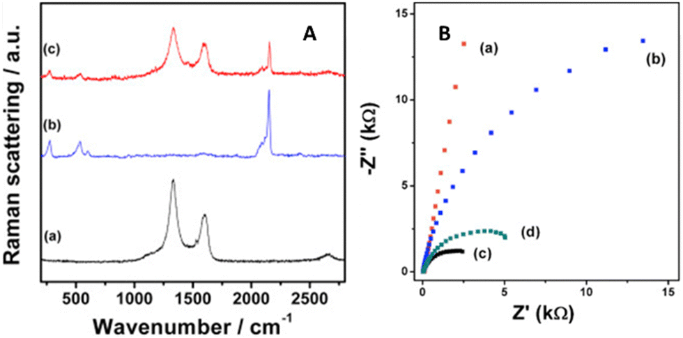 | ||
| Fig. 7 Raman stack plot (a) RGO/MWCNT, (b) PB, and (c) RGO/MWCNT/PB; (b) EIS of (a) ITO, (b) PB, (c) RGO/MWCNT, and (d) RGO/MWCNT/PB. Reprinted from ref. 25 (Copyright 2020) with permission from Elsevier. | ||
5. Outside the −0.2 to +0.3 V range, greater graphene exposure increases activity
In the electrochemical detection of uric acid, the reduction reaction for its detection takes place at +0.5 V.28 This potential is outside the Kislenko voltage range (−0.2 to +0.3 V), where defects would influence sensitivity. Instead, the degree of graphene sheet exposure was proportional to the measured current. We have observed a precise instance of MWCNT disentanglement in our laboratory accompanying maximum current readings for a ZnO/COOH-MWCNT composite. The Raman D/G band ratio for sonication times ranging from 60, 120, 150, and 165 min (Fig. 8, right) corresponded precisely with observed disentanglement in the TEM (Fig. 8, left) for these same samples. As sonication ensued, the MWCNT entanglement varied. The greater the MWCNT disentanglement, the greater the sp2 carbon within the graphene sheet was exposed. Maximum disentanglement occurred at 150 min. The current measured by the composite was directly proportional to the exposed MWCNT graphene (Fig. 8E, right axis). Entanglement of the MWCNTs otherwise attenuated signal from sp2 carbon, resulting in a higher ID/IG ratio. The conditions for these experiments were mild (carried out at room temperature and standard pressure) such that no changes in MWCNT curvature in the underlying substrate would occur. Aside from entanglement, TEM images showed a consistent morphology change of the MWCNTs at various sonication times. The degree of disentanglement maximized at the 150 min sonication time and then decreased afterward. The biosensing analyte signal for uric acid increased by as much as 9.8-fold. Since there was no increase in sp3 carbon during the sonication (as observed in the Raman and XPS spectra), we conclude that similar to the previous studies by Xing et al.9 and Hull et al.10 involving Pt NPs, defects only (or predominantly) played a role in attaching ZnO NPs to the CNM surface, enabling the sensor's electrocatalytic performance. The greater the degree of exposed graphene, the greater the electrical conductivity was observed.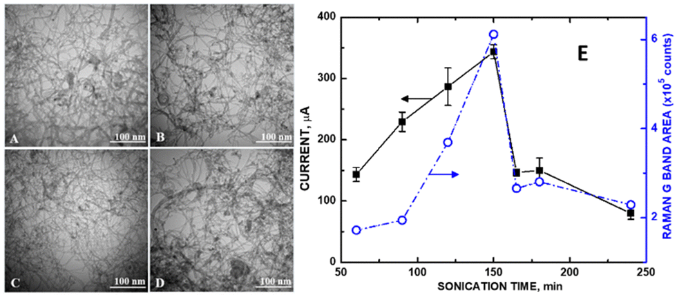 | ||
| Fig. 8 TEM of refluxed ZnO/COOH-MWCNTs at (A) 60, (B) 120, (C) 150, and (D) 165 min of sonication; (E) potentiostat current of 10 mM uric acid in PBS (pH 7) from CVs (left axis) and Raman G band integrated peak areas (right axis). Reprinted from ref. 28 (Open Access 2018) with permission from MDPI. | ||
In a study by Zakrzewska et al.,29 PB was incorporated into a Pt NP-reduced graphene oxide (PB/Pt/RGO) composite, which increased the number of defects of the electrocatalyst for the oxygen reduction reaction in 0.5 M H2SO4, important for the proton exchange fuel cell reactions. The overall peak current, which had a maximum +0.6 V standard potential, was compared with the relatively defect-rich, low-exposed graphene with that of the Pt NP-reduced graphene oxide composite without PB (Pt/RGO). The current was greater for the ORR for the Pt/RGO than that had fewer defects and higher exposed graphene (ID/IG = 1.35) than for PB/Pt/RGO (ID/IG = 1.49), which is a trend consistent for standard redox voltages outside −0.2 to +0.3 V.
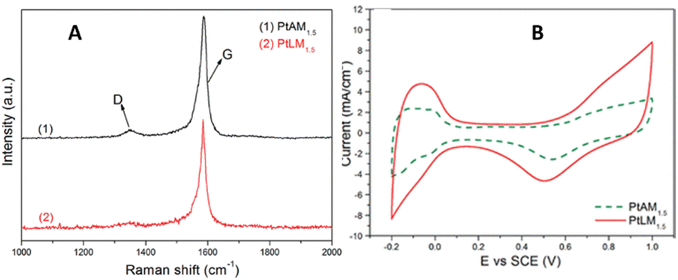
A similar phenomenon has been observed for methanol oxidation at a standard potential of +0.5 V for Pt NP-MWCNT composite. For electrochemical reactions pertaining to the direct methanol fuel cell, low-defect MWCNTs with tethered Pt nanoparticles, 2–5 nm in diameter, were uniformly dispersed onto the sidewalls and were found to be highly effective for the direct methanol fuel cell reaction.6 The lower the defect density, the higher the measured current observed. For the acid-treated MWCNT-Pt nanocomposite with a feeding ratio of Pt-to-MWCNTs of 1.5-to-1 (PtAM1.5), the ID/IG = 0.0538 (determined from the integrated Raman D and G band integrated peak area ratios in Fig. 9) led to a forward anodic peak current-to-reverse anodic peak current ratio, IF/IR = 0.83. In the case of the low-defect composite using the same feeding ratio (PtLM1.5), the measured ID/IG = 0.0524, resulting in IF/IR = 2.94. Hence, the greater exposed graphene for this electrochemical reaction had a greater than 3.5-fold increase in IF/IR current. The measured charge transfer resistance was 24.99 Ω with excellent electrocatalytic activity with a forward anodic peak current density of 47.37 mA cm−2.
 | ||
| Fig. 9 (A) Raman stack plot of PtAM1.5 and PtLM1.5; CVs of PtAM1.5 and PtLM1.5. Reprinted from ref. 14 (Copyright 2011) with permission from the American Chemical Society. | ||
For a similar composite consisting of Pt NPs on low-defect 3D carbon nanotube/nitrogen-doped graphene hybrid aerogels (Pt/LDCNT-NG), methanol oxidation occurred at +0.4 and +0.7 V standard potentials.7 The electrocatalytic activity was quantified using CVs in N2-saturated 0.5 M H2SO4 solution. Pt/DCNT-NG had an ECSA = 132.4 m2 g−1, while the Pt/NG had an ECSA = 58.1 m2 g−1. Current readings for GO, graphene (G), n-doped graphene (NG), and Pt nanoparticles tethered to graphene (Pt/G) were compared. In comparing the Raman ID/IG ratios (values in parentheses) between GO (0.87), G (1.03), NG (0.16), Pt/G (1.07), and Pt/LDCNT-NG (0.26), the Pt/LDCNT-NG composite exhibited the largest current reading in this series of carbon nanotube aerogel composites. Of the Pt-containing composites, the graphene architecture with the lowest ID/IG ratio also had the highest specific electrochemical surface areas (ECSA).
Cobalt and nitrogen-doped on reduced graphene oxide (N/RGO) with Co nanoparticles (Co@Co-N/RGO) is a useful catalyst for the ORR in the direct methanol fuel cell reaction, took place at +0.848 V; its activity was comparable to standard Pt nanoparticles deposited on carbon.30 Accompanying the high voltage, Raman spectra showed that more defects correlated with a diminished current density, which correlated with increased exposed sp2 carbon. In comparative Raman intensity measurements, the ID/IG band ratios for the RGO, N/RGO, and Co@Co-N/RGO were 1.02, 1.05, and 0.95, respectively. The electrocatalytic activity was governed by the degree of exposed graphene, where increasing current density across the electroactive surface correlated with greater exposed graphene, denoted by the ID/IG ratio.
To explore whether the effects of current are universally proportional to graphene sheet exposure, we carried out experiments on an array of saccharide-based carbon dots, where the ID/IG ratio was varied based on the ‘sweet taste’ characteristic (which summarizes molar volume, solute/solute interactions, and intramolecular H-bonding) of the saccharide precursors.31 Acetaminophen (APAP) was used as the probe molecule for redox detection using galactose CDs (GalCDs), lactose CDs (LacCDs), and glucose CDs (GluCDs) (Fig. 10A). Noteworthy is the fact that since CDs are zero-dimensional in morphology, the effect of variations in graphene sheet curvature can be eliminated as a variable that could produce additional D band intensity as an experimental artifact. Higher sp2-to-sp3 carbon ratios (in parentheses) within this CD series correlated with higher sensitivity for the measurement of APAP according to the measured Raman IG/ID values: GalCDs (10.18) > LacCDs (9.30) > GluCDs (6.53) (Fig. 10B). Currents were measured at redox voltages greater than +0.5 V. GalCDs, having the greatest sensitivity for APAP, had an oxidation voltage of +0.549 V. Hence, the observation for the Kislenko trend was evident for CDs.
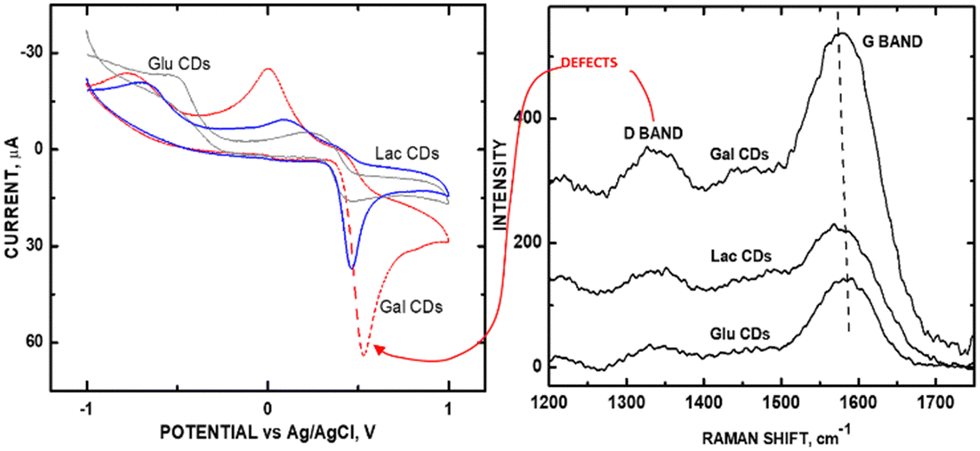 | ||
| Fig. 10 (A) CVs of GluCDs, LacCDs, and GalCDs; (B) Raman stack plot of GluCDs, LacCDs, and GalCDs. Reprinted from ref. 31 (Copyright 2021) with permission from Wiley-VCH. | ||
6. Charge carriers interacting with defects reduce electrochemical activity
The introduction of charge carriers affected (Fig. 1) CNM conductivity. Salehi et al.18 showed that graphene conductivity increased when healed of its defects via plasma treatment. In this experiment, the decrease in sp3 carbon was corroborated by SEM, showing a reduction of surface roughening, a decrease in peak areas of the D and 2D bands observed under Raman spectroscopy, and the accompanying increase in slopes of the I–V curves of measured current passed through the surface. Healed defects led to greater G band intensity and increased electrocatalytic activity. The increase in conductivity was attributed to the scattering of charged impurities,32 postulated to originate from the presence of sparse amounts of hydroxy and carboxyl function groups as indicated by observed deviations from linear I–V curves of the graphene surfaces after plasma treatment. Bonding functional groups (such as those containing oxygen atoms, e.g., –COOH, COH, etc.) reduces the electrical conductivity of graphene. Defects lessen the mobility of charge carriers that subsequently increase resistivity and thereby lowering conduction.33,34 Under these conditions, conduction is inversely proportional to the number of graphene layers;35 hence, a single graphene sheet has the highest conduction point. Charged impurities are known to create a spatially inhomogeneous distribution of Coulombic potential. With a low carrier density, the system broke into puddles of electrons and holes.36It should also be noted that charge mobility from alkali ions, e.g., K+ and Na+, ubiquitous in many electrochemical systems, would not be involved in current density reduction by defects within the graphene structure, as showdown by Jeong et al.37 In their experiments, direct intercalation of alkali-metal cations from K+ and Na+ were incorporated for the electrochemical redox reaction of Prussian Blue on a graphene surface, comparing them with controls where Na+ and K+ ions were not involved. CV data showed that PB films passivated with monolayer graphene still underwent electrochemical redox reactions with these alkali ions present despite their inability to penetrate the graphene and be incorporated into PB; they showed that a transparent graphene electrode covering PB can still be used as an effective H2O2 transducer. The graphene overlayers did not hamper ionic interactions of the alkali cations with FeIII ions in PB, indicating that defects within the graphene (because of its transparency to the alkali cations) do not affect the charge mobility of these cations and, therefore, would not result in a current decrease.
7. Conclusions
The following general trends governing the correlation of exposed sp2 graphene and sp3 defects within a host of CNMs with electrochemical sensitivity within redox reactions in aqueous solution can be ascertained. If the electrochemical redox reaction takes place at voltages between −0.2 to +0.3 V, the defect density within the graphene structure directly correlating with higher Coulombic conductivity is anticipated. That is, the greater the density, the greater the electrochemical signal is observed. If, on the other hand, the redox reaction occurs outside this span of voltages, electrochemical signal intensity varies directly with the degree of exposed graphene. The presence of charged impurities can skew the proportional relationship of defect density to electrical conduction, in which defects hamper charge mobility instead of serving as electron acceptors. While examining electrocatalytic behavior in carbon dots (the newest of these carbon nanomaterials) is still in its infancy, we postulate that this same trend governing their conductivity will be observed in emerging experiments using them as electrochemical catalyst supports.Author contributions
C.C. Chusuei: conceptualization, software, supervision, writing – original draft; R.C. Nepal: data curation (Fig. 5B), writing – review and editing.Conflicts of interest
There are no conflicts to declare.Acknowledgements
We thank Braedyn Hollingsworth and Nate Martinez for their assistance in curve-fitting the Raman spectra in the literature mentioned to determine the ID/IG ratios discussed in this article. The National Science Foundation supported this work under Grant No. 1920293.Notes and references
- G. Speranza, Nanomaterials, 2021, 11, 967, DOI:10.3390/nano11040967.
- R. R. Pandey and C. C. Chusuei, Molecules, 2021, 26, 6674, DOI:10.3390/molecules26216674.
- M. S. Dresselhaus and M. Terrones, Proc. IEEE, 2013, 101, 1522–1535, DOI:10.1109/JPROC.2013.2261271.
- F. Tuinstra and J. L. Koenig, J. Chem. Phys., 2003, 53, 1126–1130, DOI:10.1063/1.1674108.
- A. C. Ferrari and D. M. Basko, Nat. Nanotechnol., 2013, 8, 235–246, DOI:10.1038/nnano.2013.46.
- H. Huang, D. Sun and X. J. Wang, J. Phys. Chem. C, 2011, 115, 19405–19412, DOI:10.1021/jp204293h.
- M. Yan, Q. Jiang, T. Zhang, J. Wang, L. Yang, Z. Lu, H. He, Y. Fu, X. Wang and H. Huang, J. Mater. Chem. A, 2018, 6, 18165–18172, 10.1039/C8TA05124K.
- L.-P. Ma, W. Ren and H.-M. Cheng, Small Methods, 2019, 3, 1900049, DOI:10.1002/smtd.201900049.
- Y. Xing, L. Li, C. C. Chusuei and R. V. Hull, Langmuir, 2005, 21, 4185–4190, DOI:10.1021/la047268e.
- R. V. Hull, L. Li, Y. Xing and C. C. Chusuei, Chem. Mater., 2006, 18, 1780–1788, DOI:10.1021/cm0518978.
- R. Saito and H. Kataura, in Carbon Nanotubes: Synthesis, Structure, Properties, and Applications, ed. M. S. Dresselhaus, G. Dresselhaus and P. Avouris, Springer, Berlin, Heidelberg, 2001, pp. 213–247 DOI:10.1007/3-540-39947-X_9.
- A. C. Ferrari, Solid State Commun., 2007, 143, 47–57, DOI:10.1016/j.ssc.2007.03.052.
- V. A. Kislenko, S. V. Pavlov and S. A. Kislenko, Electrochim. Acta, 2020, 341, 136011, DOI:10.1016/j.electacta.2020.136011.
- H. Huang, D. Sun and X. Wang, J. Phys. Chem. C, 2011, 115, 19405–19412, DOI:10.1021/jp204293h.
- E. Picheau, A. Impellizzeri, D. Rybkovskiy, M. Bayle, J.-Y. Mevellec, F. Hof, H. Saadaoui, L. Noé, A. C. Torres Dias, J.-L. Duvail, M. Monthioux, B. Humbert, P. Puech, C. P. Ewels and A. Pénicaud, ACS Nano, 2021, 15, 596–603, DOI:10.1021/acsnano.0c06048.
- A. K. Gupta, C. Nisoli, P. E. Lammert, V. H. Crespi and P. C. Eklund, J. Phys.: Condens. Matter, 2010, 22, 334205, DOI:10.1088/0953-8984/22/33/334205.
- S. Osswald, M. Havel and Y. Gogotsi, J. Raman Spectrosc., 2007, 38, 728–736, DOI:10.1002/jrs.1686.
- M. Salehi, P. Bastani, L. Jamilpanah, A. Madani, S. M. Mohseni and B. Shokri, Sci. Rep., 2021, 11, 20334, DOI:10.1038/s41598-021-99421-7.
- A. J. Slate, D. A. C. Brownson, A. S. A. Dena, G. C. Smith, K. A. Whitehead and C. E. Banks, Phys. Chem. Chem. Phys., 2018, 20, 20010–20022, 10.1039/C8CP02196A.
- D. Nikolaievskyi, M. Torregrosa, A. Merlen, S. Clair, O. Chuzel, J.-L. Parrain, T. Neisus, A. Campos, M. Cabie, C. Martin and C. Pardanaud, Carbon, 2023, 203, 650–660, DOI:10.1016/j.carbon.2022.12.010.
- M. D. Jerez-Masaquiza, L. Fernández, G. González, M. Montero-Jiménez and P. J. Espinoza-Montero, Nanomaterials, 2020, 10, 1328, DOI:10.3390/nano10071328.
- L. Chen, X. Wang, X. Zhang and H. Zhang, J. Mater. Chem., 2012, 22, 22090–22096, 10.1039/C2JM34541B.
- L. Xu, G. Zhang, J. Chen, Y. Zhou, G. Yuan and F. Yang, J. Power Sources, 2013, 240, 101–108, DOI:10.1016/j.jpowsour.2013.03.156.
- Y. Zhang, X. Sun, L. Zhu, H. Shen and N. Jia, Electrochim. Acta, 2011, 56, 1239–1245, DOI:10.1016/j.electacta.2010.11.011.
- S. C. Silva, R. M. Cardoso, E. M. Richter, R. A. A. Munoz and E. Nossol, Mater. Chem. Phys., 2020, 250, 123011, DOI:10.1016/j.matchemphys.2020.123011.
- R. R. Pandey, Y. Guo, Y. Gao and C. C. Chusuei, Anal. Chem., 2019, 91, 10573–10581, DOI:10.1021/acs.analchem.9b01636.
- R. Shanmugam, P. Barathi and A. S. Kumar, Colloids Surf., A, 2014, 452, 129–137, DOI:10.1016/j.colsurfa.2014.03.089.
- S. C. Das, R. R. Pandey, T. Devkota and C. C. Chusuei, Chemosensors, 2018, 6, 65, DOI:10.3390/chemosensors6040065.
- B. Zakrzewska, B. Dembinska, S. Zoladek, I. A. Rutkowska, J. Żak, L. Stobinski, A. Małolepszy, E. Negro, V. Di Noto, P. J. Kulesza and K. Miecznikowski, J. Electroanal. Chem., 2020, 875, 114347, DOI:10.1016/j.jelechem.2020.114347.
- D. Zhao, J. Dai, N. Zhou, N. Wang, X. Peng, Y. Qu and L. Li, Carbon, 2019, 142, 196–205, DOI:10.1016/j.carbon.2018.10.057.
- C. C. Chusuei, C. J. Clark, R. R. Pandey, E. T. Williams, C. Shuxteau, E. S. Seven and R. M. Leblanc, Electroanalysis, 2021, 33, 2261–2266, DOI:10.1002/elan.202100381.
- A. Pirkle, J. Chan, A. Venugopal, D. Hinojos, C. W. Magnuson, S. McDonnell, L. Colombo, E. M. Vogel, R. S. Ruoff and R. M. Wallace, Appl. Phys. Lett., 2011, 99, 122108, DOI:10.1063/1.3643444.
- L. Vicarelli, S. J. Heerema, C. Dekker and H. W. Zandbergen, ACS Nano, 2015, 9, 3428–3435, DOI:10.1021/acsnano.5b01762.
- A. Lherbier, S. M.-M. Dubois, X. Declerck, Y.-M. Niquet, S. Roche and J.-C. Charlier, Phys. Rev. B: Condens. Matter Mater. Phys., 2012, 86, 075402, DOI:10.1103/PhysRevB.86.075402.
- M.-S. Cao, X.-X. Wang, W.-Q. Cao and J. Yuan, J. Mater. Chem. C, 2015, 3, 6589–6599, 10.1039/C5TC01354B.
- S. Adam, E. H. Hwang, V. M. Galitski and S. D. Sarma, Proc. Natl. Acad. Sci. U. S. A., 2007, 104, 18392–18397, DOI:10.1073/pnas.0704772104.
- D. W. Jeong, K. Kim, G. Lee, M. Kang, H. Chang, A.-R. Jang and J.-O. Lee, ACS Nano, 2022, 16, 9278–9286, DOI:10.1021/acsnano.2c01786.
| This journal is © The Royal Society of Chemistry and the Centre National de la Recherche Scientifique 2024 |